JP3944095B2 - Holding device - Google Patents
Holding device Download PDFInfo
- Publication number
- JP3944095B2 JP3944095B2 JP2003048365A JP2003048365A JP3944095B2 JP 3944095 B2 JP3944095 B2 JP 3944095B2 JP 2003048365 A JP2003048365 A JP 2003048365A JP 2003048365 A JP2003048365 A JP 2003048365A JP 3944095 B2 JP3944095 B2 JP 3944095B2
- Authority
- JP
- Japan
- Prior art keywords
- optical element
- holding device
- optical
- holding
- optical system
- Prior art date
- Legal status (The legal status is an assumption and is not a legal conclusion. Google has not performed a legal analysis and makes no representation as to the accuracy of the status listed.)
- Expired - Fee Related
Links
Images


Classifications
-
- G—PHYSICS
- G02—OPTICS
- G02B—OPTICAL ELEMENTS, SYSTEMS OR APPARATUS
- G02B7/00—Mountings, adjusting means, or light-tight connections, for optical elements
- G02B7/02—Mountings, adjusting means, or light-tight connections, for optical elements for lenses
-
- G—PHYSICS
- G02—OPTICS
- G02B—OPTICAL ELEMENTS, SYSTEMS OR APPARATUS
- G02B7/00—Mountings, adjusting means, or light-tight connections, for optical elements
- G02B7/18—Mountings, adjusting means, or light-tight connections, for optical elements for prisms; for mirrors
- G02B7/182—Mountings, adjusting means, or light-tight connections, for optical elements for prisms; for mirrors for mirrors
Description
【0001】
【発明の属する技術分野】
本発明は、一般には、レンズを搭載する精密機械、特に、露光装置等の投影光学系に係り、更に詳細には、半導体素子、撮像素子(CCD等)又は薄膜磁気ヘッド等を製造するためのリソグラフィー工程に使用される露光装置において、原版(例えば、マスク又はレチクル(なお、本出願ではこれらの用語を交換可能に使用する。))の像を被処理体(例えば、半導体ウェハ用の単結晶基板、液晶ディスプレイ(LCD)用のガラス基板)に投影露光する際、より正確な結像関係を得るための光学素子の保持装置に関する。
【0002】
【従来の技術】
フォトリソグラフィー技術を用いてデバイスを製造する際に、マスクに描画された回路パターンを投影光学系によってウェハ等に投影して回路パターンを転写する投影露光装置が従来から使用されている。投影光学系は、回路パターンからの回折光をウェハの上に干渉させて結像させる。
【0003】
近年の電子機器の小型化及び薄型化への要請を実現するためには、電子機器に搭載されるデバイスを高集積化する必要があり、転写される回路パターンの微細化、即ち、高解像度化がますます要求されている。高解像力を得るためには、光源の波長を短くすること、及び、投影光学系の開口数(NA)を上げることが有効であり、同時に投影光学系の収差を小さく抑えなくてはならない。
【0004】
投影光学系を構成するレンズ、ミラーなどの光学素子に変形が生じると、変形前後で光路が屈折し、一点に結像するべき光線が一点に収束せずに収差を生じる。収差は位置ずれを招いてウェハ上の回路パターンの短絡を招く。一方、短絡を防止するためにパターン寸法を広くすれば微細化の要求に反する。従って、収差が小さい投影光学系を実現するためには、投影光学系を構成する光学素子を形状を変化させることなく投影光学系内に保持して、光学素子が有する本来の光学的性能を最大限に引き出す必要がある。
【0005】
図12は、従来の光学素子1100の保持装置1000を示す概略断面図である。図12を参照するに、光学素子1100の外径を保持部材1200の内径に嵌合、又は、ある程度の間隙を設けて配置し、保持部材1200の内径に設けられた支持部1200aに光学素子1000の一方の面を接触させ、光学素子1100の外径と保持部材1200の内径との間隙に接着剤1300を注入する。接着剤1300が硬化すると、光学素子1100は、保持部材1200に一体的に保持される。このように、保持装置1000に保持された光学素子1100は、図13に示すように、同様に保持装置1000に保持された複数の光学素子1100と共に、筐体2000内に保持されて光学系を構成する。図13は、従来の保持装置1000で保持された光学素子1100で構成された光学系を示す概略断面図である。
【0006】
一般に、光学素子1100が保持部材1200と接触している支持部1200aの形状は、図14に示すように、光学素子1100の回転中心軸に対して360°の範囲で接触するように構成されている。しかし、機械加工により支持部1200aの平坦度を0にすることは困難であり、360°の範囲で接するように構成されていても、微視的には光学素子1100と保持部材1200とは複数の点で接触することになる。かかる状態で重力の影響を受けた場合、光学素子1100は、自重によって保持部材1200との接触点を頂点とした波型に変形する。特に、近年の投影光学系の高NA化により、レンズが大口径化しているのでレンズ容積も大きくなり、自重による変形が発生しやすくなっている。ここで、図14は、従来の保持装置1000の保持部材1200を示す概略構成図である。
【0007】
投影光学系においては、複数の光学素子(ミラーやレンズ等)の諸々の誤差により生じる収差を、相互の光学素子の組み合わせや位置関係を調整することで補正しているが、光学素子の面形状に関してはナノメートルオーダーの変形を考慮する必要がある。しかし、保持装置1000を用いた場合には、使用する光学素子1100と保持部材1200の組み合わせによって両者の接触点が変わり、それに伴って変形後の面形状も変わるため、部材が異なる装置間のばらつきが生じ収差の補正が非常に煩雑となる。
【0008】
そこで、図15に示すように、支持部1500aを光学素子1100の回転中心に対して120°間隔の3箇所のみに残した保持部材1500が用いられる場合もある。光学素子1100は、常に120°間隔の3箇所で保持部材1500に接触し支持されるので、重力によって接触点(即ち、支持部1500a)を頂点とした山を120°間隔で有する波型に変形する。ここで、図15は、従来の保持装置の保持部材1500を示す概略構成図である。
【0009】
幾何学的には平面は3点で定義されるので、保持部材1500の加工精度によらず3箇所の支持部1500aは常に同一平面上にあり、支持部1500aと接触する光学素子1100は、組み合わせる保持部材1500が変わってもほぼ同様の条件で保持されることになる。
【0010】
一般に、光学素子は山を3つ有する波型の形状に変形すると、波面収差の3角成分を生じるが、光学系を構成する他の光学素子との組み合わせにより補正が可能である。従って、部材が異なる装置間のばらつきを抑えることができ、光学素子の回転中心軸に対して360°の範囲で接触するように構成された保持部材1200よりも収差の補正が容易になるという利点がある。
【0011】
【発明が解決しようとする課題】
しかしながら、ミラーやレンズ等の光学素子は、光学的な性質や製作性の都合によって石英等の光学ガラス材で作製されることが多く、一方、光学素子の保持部材については、強度や加工性の点から金属材料で製作される。換言すれば、光学部材と保持部材の材質は互いに異なり、両者の線膨張係数には差がある。従って、光学系の置かれる環境温度の変化や光学素子の発熱などにより光学素子や保持部材の温度が変化した場合、線膨張係数の違いのために光学素子と保持部材の伸縮量に差が生じる。
【0012】
図12乃至図15に示した従来の保持装置では、接着剤を介して連結されている光学素子の外径と保持部材の内径の伸縮量に差が生じ、光学素子は半径方向の引張り又は圧縮の強制変位を受け、光学素子の上下面も変形する。その結果、光学素子の光学的性能が変化し、複数の光学素子から構成される光学系の光学的性能も変化してしまう。即ち、温度が変化することによって装置の光学性能が劣化するという問題を招いてしまう。
【0013】
特に、光学素子の回転中心軸に対して360°の範囲で接触するように構成された保持装置では、上述したように、微視的には複数の点で光学素子と接触し、かかる接触点の位置が異なるため、温度が変化したときの光学素子の形状変化にもばらつきが生じ、そのために生じる収差の変化を予測して(即ち、温度変化に従って)補正することは非常に困難である。
【0014】
一方、光学素子と3箇所で接触するように構成された保持装置では、光学素子と保持部材の伸縮量の差によって、接着剤を介して光学素子の外径に強制変位を受けるために光学素子の形状は変化するが、波型に変形した頂点の回転方向の変位は変わらず、山の大きさが増減するように変化する。これにより、光学素子の変形による波面収差の3角成分が温度によって変化することになるが、波面収差の3角成分の変化量を温度変化に伴って補正することは困難である。
【0015】
そこで、本発明は、環境温度の変化によって光学素子に生じる波面収差の3角成分の変化を抑制し、光学性能の劣化を防止することができる保持装置を提供することを例示的目的とする。
【0016】
【課題を解決するための手段】
上記目的を達成するために、本発明の一側面としての保持装置は、中心軸を重力方向と一致させて略回転対称形状の光学素子を保持する保持装置であって、前記光学素子の中心軸に関して略120°間隔の3箇所に設けられた支持部を介して前記光学素子を保持する保持部材と、前記光学素子の外径部と前記保持部材とを接合する接合部材とを有し、前記光学素子の反重力方向側の面と前記中心軸との交点を原点として前記中心軸の反重力方向をz軸の正とする座標系(z)を設定し、前記光学素子の重心のz座標をzg、前記接合部材が前記光学素子と接合するz軸方向の幅の中央位置のz座標をzb、前記接合部材が前記光学素子と接合するz軸方向の幅をwbとしたときに、|(zb−0.6wb)−(zg+1.2)|≦1の関係を満たすことを特徴とする保持装置。前記光学素子は、光学ミラーであることを特徴とする。前記接合部材は、接着剤であることを特徴とする。前記接合部材は、櫛型バネであることを特徴とする。前記保持部材は、前記光学素子の中心軸を中心とする円環状形状であることを特徴とする。前記接合部材は、前記前記光学素子の外径部の全周に亘って前記保持部材と接合することを特徴とする。
【0017】
本発明の別の側面としての光学系は、略回転軸対称形状の光学素子と、前記光学素子を保持する上述の保持装置とを有することを特徴とする。
【0018】
本発明の更に別の側面としての光学装置は、複数の光学素子から構成され、前記複数の光学素子のうち少なくとも一は上述の保持装置に保持されることを特徴とする。
【0019】
本発明の更に別の側面としての露光装置は、上述の保持装置と、前記保持装置に保持された光学素子を介してマスク又はレチクルに形成されたパターンを被処理体に露光する光学系とを有することを特徴とする。
【0020】
本発明の更に別の側面としてのデバイス製造方法は、上述の露光装置を用いて被処理体を露光するステップと、露光された前記被処理体に所定のプロセスを行うステップとを有する。
【0021】
本発明の他の目的及び更なる特徴は、以下添付図面を参照して説明される好ましい実施例によって明らかにされるであろう。
【0022】
【発明の実施の形態】
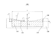
以下、添付図面を参照して、本発明の例示的な保持装置及び露光装置について説明する。但し、本発明は、これらの実施例に限定するものではなく、本発明の目的が達成される範囲において、各構成要素が代替的に置換されてもよい。例えば、本実施形態では、保持装置100を例示的に露光装置200の投影光学系230に適用しているが、露光装置200の照明光学系214、その他周知のいかなる光学系に適用してもよい。ここで、図1は、本発明の一側面としての保持装置100の例示的一形態を示す概略断面図である。重力方向は、光学素子110の光軸方向と一致し、図面矢印方向である。
【0023】
図1において、100は保持装置、110は光学系を構成する光学素子で回転対称形状を有し、その中心軸が重力方向と一致している。本実施形態では、光学素子110は、光学ミラーで構成され、ミラー面が反重力方向、即ち、図面上側になるように配置されている。但し、光学素子110は光学ミラーに限定するものではなく、例えば、レンズ、平行平板ガラス、プリズム、フレンネルゾーンプレート、キノフォーム、バイナリオプティックス、ホログラム等の回折光学素子を含む。
【0024】
保持部材120は光学素子110の中心軸を中心とする円環状形状を有し、図2に示すように、光学素子110の中心軸に関して120°間隔の3箇所に設けられた支持部122を介して光学素子110を保持する。ここで、図2は、図1に示す保持部材120の概略構成図である。保持部材120及び支持部122は、例えば、実質的に光学素子110の線膨張係数と等しい線膨張係数を有する材料から構成される。このように構成すれば、温度環境変動時に、線膨張係数の違いから生じる光学素子110と保持部材120の相対変位により、光学素子110が支持部122を介して外力を受けて変形したり、ストレスがかかったりすることを防止することができる。
【0025】
130は光学素子110と保持部材120とを接合する接合部材を、232は後述する露光装置200の投影光学系230の鏡筒を示している。接合部材130は、本実施形態では、接着剤で構成され、かかる接着剤は脱ガスが極小であるものを選択する。
【0026】
このような構成において、保持部材120の支持部122に、光学素子110の重力方向の面(即ち、ミラー面の対向面)が支持されるように接触させ、光学素子110を保持部材120に嵌合、又は、ある程度の間隙を設けて配置する。そして、光学素子110の外径部110aと保持部材120の内側面との間隙の全周(即ち、光学素子110の中心軸に対して360°の範囲)に接合部材130を注入する。接合部材130は、本実施形態では、接着剤であるため、かかる接着剤が硬化することにより光学素子110は保持装置100に一体的に保持される。
【0027】
ここで、図1に示す保持装置100において、有限要素解析を用いて環境温度が変化した場合の影響を求める。図3に示すように、光学素子110の中心軸を反重力方向を正とするz軸とし、z軸と反重力方向側の面(ミラー面)との交点を原点O、原点Oを通り光学素子110の半径方向をr、z軸に垂直であり支持部122に向かう方向をθ=0としてz軸周りに角度θをとった円筒座標系(r,θ,z)を設定する。また、Pgは光学素子110の重心であり、光学素子110は回転対称形状であるため重心は中心軸上にあるので座標を(0,0,zg)とする。光学素子110と保持部材120との間隙に注入された接合部材130のz軸方向の幅をwb、接合部材130のz軸方向の幅の中央位置を接合位置と称し、そのz座標をzbとする。更に、光学素子110の直径をD、中心軸上の厚さをL、光学素子110の曲率半径をRoとする。ここで、図3は、本発明の保持装置100の座標系を示す概略断面図である。
【0028】
かかる保持装置100の有限要素解析のモデルを図4に示す。光学素子110は、120°等間隔の3箇所で支持され、中心軸方向に重力を受け、外周部110aに接合部材130が配置されていることから、境界条件の対称性を考慮すると、有限要素解析モデルとしては0≦θ≦60°の範囲について考えればよい。任意の点の変位を円筒座標系で(Ur,Uθ,Uz)とすると、境界条件としてはθ=0°、及び、θ=60°の対称面において変位成分Uθ=0、光学素子110に保持部材120に支持部122が接触する部分を点接触とみなし変位成分Uz=0という変位拘束をそれぞれ設定する。また、z軸の負方向に重力加速度Gを設定する。更に、環境温度が変化したときの光学素子110と保持部材120の伸縮量の差により光学素子110に加わる強制変位を、外径部110aの接合部材130の接合範囲に変位成分Urとして設定する。なお、それ以外の変位成分については非拘束とする。ここで、図4は、本発明の保持装置100の有限要素解析モデルを示す概略図である。
【0029】
図4を参照するに、光学素子110の材質を石英(縦弾性係数7.3×10¹⁰[Pa]、ポアソン比0.18、密度2.2×10³[Kg/m3])、重力加速度G=9.80665[m/s2]とし、接合部材130の接合範囲の変位境界条件は、環境温度が変化する前の変位成分Urを非拘束、環境温度が変化したときの変位成分Ur=−0.1[mm](圧縮)と設定し、光学素子110の形状に関して、曲率半径Ro=150[mm]、中心軸上厚さL=10[mm]、直径D=110[mm]、及び、接合に関する接合幅wb=2[mm]を基準として各々を独立して変化させて弾性静変形の有限要素解析を行った。
【0030】
ここで、光学素子110の変形について、有限要素解析で求められたミラー面上の各点の変位成分Uzを、収差論などで用いられるZernike多項式により、図3の円筒座標系(r,θ,z)に関して展開する。光学素子110のミラー面の変形は120°間隔で3つの山を有する波型となり、120°で回転対称となる。従って、求められたZernike多項式の項のうち、θを含まない、所謂、軸対称項と、sin3θ、cos3θを含む、所謂、3θ項以外の係数は直交条件により0となる。
【0031】
このうち、上述した波面収差の3角成分に影響があるのは3θ項であり、特に、3つの山を有する波型に変形する場合は、3θ項のちrの次数が最も低い、r3sin3θ、r3cos3θという項の係数が、それよりrの次数が高い項の係数よりもはるかに大きくなるので、これら2つの項の係数の和を3θ変形と呼ぶこととし、環境温度の変化による3θ変形の変化量をδ(3θ)とすることとする。
【0032】
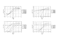
このようにして求めた3θ変形の変化量を、横軸に接合位置の座標zbをとり、縦軸に3θ変形の変化量δ(3θ)をとって表示すると図5のようになる。図5は、本発明の保持装置100において、光学素子110と保持部材120との接合位置と光学素子110の3θ変形の変化量との関係を示すグラフである。光学素子110の形状を基準として、図5(a)は曲率半径Roのみを、図5(b)は中心軸上厚さLのみを、図5(c)は直径Dのみを、図5(d)は接合幅wbのみを、それぞれ変化させて有限要素解析を行った結果である。
【0033】
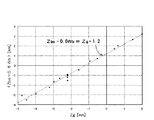
図5(a)乃至図5(d)を参照するに、いずれの場合でも3θ変形の変形量δ(3θ)が0となる接合位置の座標zbが存在する。そして、図5(a)乃至図5(d)において、3θ変形の変化量δ(3θ)が0となるときの接合位置の座標zbをzb0とし、有限要素解析を行った。各結果のデータについて、横軸に光学素子110の重心Pgの座標zg、縦軸に(zb0−0.6wb)の値をとって表示すると図6のようになる。図6は、本発明の保持装置100において、光学素子110の重心Pgの位置と光学素子110と保持部材120との接合位置との関係を示すグラフである。
【0034】
図6を参照するに、光学素子110の重心Pgの座標zgと(zb0−0.6wb)との間にはほぼ線形な関係が成り立ち、以下の数式1で表される関係の直線を同図上に描画すると、各データは同直線上にほぼのっていることがわかる。
【0035】
【数1】

即ち、数式1の関係を満たすように接合部材130を配置したとき、光学素子110は環境温度が変化しても3θ変形の変化がほぼ0となることがわかる。
【0037】
以上のように、光学素子110において、光学素子110の重心Pgの座標zg、接合位置の座標zb、及び、接合幅wbが数式1の関係を満たすように接合することにより、環境温度が変化しても光学素子110の3θ変形の変化が小さく、それによる波面収差の3角成分の変化も小さくなり、環境温度の変化による光学性能の劣化が起こり難い保持装置100が実現できる。
【0038】
更に、本実施形態の保持装置100を複数の光学素子から構成される光学装置に適用すれば、環境温度の変化による光学性能の劣化が起こり難い光学装置が得られる。
【0039】
但し、上述の数式1の等号を満たす場合の接合位置zbは、光学素子110の形状寸法及び接合幅wbが決まれば唯一通りに決まるが、数式1の関係式を満たす接合位置zbの近傍に接合位置を設定しても、光学系の温度変化による光学性能の劣化を低減する効果がある。実際には、設置位置を1[mm]程度の範囲に設定することは容易であるので、数式1の関係式の両辺の差分の絶対値を1[mm]以下に設定する、即ち、以下に示す数式2の関係式を満たすように接合しても効果がある。
【0040】
【数2】
なお、本実施例について述べたが、レンズ等、他の光学素子においても、光学素子の反重力方向側の面の変形に起因する収差の影響についてのみ考慮すればよい場合は、同様の効果を得ることができる。
【0042】
次に、図7を参照して、図1に示す保持装置100の変形例である保持装置100Aについて説明する。図7は、図1に示す保持装置100の変形例である保持装置100Aの例示的一形態を示す概略断面図である。なお、図7において、図1に示すのと同一の部材については、同一の参照番号を付し、重複する説明は省略する。
【0043】
図7を参照するに、保持装置100Aは、図1に示す保持装置100と同様であるが、接合部材130を、接着剤から櫛型バネ130Aに置き換えた構成をしている。
【0044】
櫛型バネ130Aは、図8に示すように、光学素子110の中心軸を中心とする円環状形状であり、内側面に多数の放射状貫通溝132Aを設けた櫛状になった接続部134Aを有する。櫛型バネ130Aは、接続部134Aの貫通溝132Aに挟まれた部分を折り曲げることによりその1つ1つが板バネとして機能するようになっている。ここで、図8は、図7に示す櫛型バネ130Aの概略構成図である。
【0045】
また、櫛型バネ130Aは、光学素子110に一体的に取り付けられ、内側面の櫛状の接続部134Aが光学素子110の外径部110aに接合し、バネ力により光学素子110を外径部110aを介して中心向きに押すようになっている。櫛型バネ130Aのバネ力により、光学素子110は保持部材120に一体的に保持される。
【0046】
保持装置100Aにおいて、環境温度が変化した際には、光学素子110と保持部材120との線膨張閨秀の差に起因する伸縮量の差は、保持装置100と同様に、櫛型バネ130Aを介して光学素子110の外径部110aに強制変位として与えられる。
【0047】
従って、図3に示すのと同様な円筒座標系(r,θ,z)を設定し、光学素子110の重心Pgの座標zg、櫛型バネ130Aと光学素子110とが接合する範囲のz軸方向の幅の中央位置のz座標をzb、同じく、接合するz軸方向の幅をwbとしたときに、数式2を満たすように構成すれば、保持装置100と同様の効果を得ることができる。
【0048】
以下、図9を参照して、本発明の保持装置100及び/又は100Aを適用した例示的な投影光学系230及び投影光学系230を有する露光装置200について説明する。ここで、図9は、本発明の一側面としての露光装置200の例示的一形態を示す概略ブロック断面図である。露光装置200は、図9に示すように、回路パターンが形成されたマスク220を照明する照明装置210と、照明されたマスクパターンから生じる回折光をプレート240に投影する投影光学系230と、プレート240を支持するステージ245とを有する。
【0049】
露光装置200は、例えば、ステップ・アンド・スキャン方式やステップ・アンド・リピート方式でマスク220に形成された回路パターンをプレート240に露光する投影露光装置である。かかる露光装置は、サブミクロンやクオーターミクロン以下のリソグラフィー工程に好適であり、以下、本実施形態ではステップ・アンド・スキャン方式の露光装置(「スキャナー」とも呼ばれる。)を例に説明する。ここで、「ステップ・アンド・スキャン方式」とは、マスクに対してウェハを連続的にスキャン(走査)してマスクパターンをウェハに露光すると共に、1ショットの露光終了後ウェハをステップ移動して、次の露光領域に移動する露光方法である。「ステップ・アンド・リピート方式」とは、ウェハの一括露光ごとにウェハをステップ移動して次のショットの露光領域に移動する露光方法である。
【0050】
照明装置210は、転写用の回路パターンが形成されたマスク220を照明し、光源部212と、照明光学系214とを有する。
【0051】
光源部212は、例えば、光源としては、波長約193nmのArFエキシマレーザー、波長約248nmのKrFエキシマレーザーなどを使用することができるが、光源の種類はエキシマレーザーに限定されず、例えば、波長約153nmのF2レーザーやYAGレーザーを使用してもよいし、その光源の個数も限定されない。また、EUV光源等を用いてもよい。例えば、独立に動作する2個の固体レーザーを使用すれば固体レーザー間相互のコヒーレンスはなく、コヒーレンスに起因するスペックルはかなり低減する。さらにスペックルを低減するために光学系を直線的又は回動的に揺動させてもよい。また、光源部212にレーザーが使用される場合、レーザー光源からの平行光束を所望のビーム形状に整形する光束整形光学系、コヒーレントなレーザー光束をインコヒーレント化するインコヒーレント化光学系を使用することが好ましい。また、光源部212に使用可能な光源はレーザーに限定されるものではなく、一又は複数の水銀ランプやキセノンランプなどのランプも使用可能である。
【0052】
照明光学系214は、マスク220を照明する光学系であり、レンズ、ミラー、オプティカルインテグレーター、絞り等を含む。例えば、コンデンサーレンズ、ハエの目レンズ、開口絞り、コンデンサーレンズ、スリット、結像光学系の順で整列する等である。照明光学系214は、軸上光、軸外光を問わずに使用することができる。オプティカルインテグレーターは、ハエの目レンズや2組のシリンドリカルレンズアレイ(又はレンチキュラーレンズ)板を重ねることによって構成されるインテグレーター等を含むが、光学ロッドや回折素子に置換される場合もある。かかる照明光学系214のレンズなどの光学素子の保持に本発明の保持装置100及び/又は100Aを使用することができる。
【0053】
マスク200は、例えば、石英製で、その上には転写されるべき回路パターン(又は像)が形成され、図示しないマスクステージに支持及び駆動される。マスク220から発せられた回折光は、投影光学系230を通りプレート240上に投影される。マスク220とプレート240は、光学的に共役の関係にある。本実施形態の露光装置200はスキャナーであるため、マスク220とプレート240を縮小倍率比の速度比でスキャンすることによりマスク220のパターンをプレート240上に転写する。なお、ステップ・アンド・リピート方式の露光装置(「ステッパー」とも呼ばれる。)の場合は、マスク220とプレート240を静止させた状態で露光が行われる。
【0054】
投影光学系230は、複数のレンズ素子のみからなる光学系、複数のレンズ素子と少なくとも一枚の凹面鏡とを有する光学系(カタディオプトリック光学系)、複数のレンズ素子と少なくとも一枚のキノフォームなどの回折光学素子とを有する光学系、全ミラー型の光学系等を使用することができる。色収差の補正が必要な場合には、互いに分散値(アッベ値)の異なるガラス材からなる複数のレンズ素子を使用したり、回折光学素子をレンズ素子と逆方向の分散が生じるように構成したりする。
【0055】
かかる投影光学系230のレンズなどの光学素子の保持に本発明の保持装置100及び/又は100Aを使用することができる。保持装置100及び100Aは、図1及び図7に示すように、半径方向の変形を吸収することができるバネ部材234によって投影光学系230の鏡筒232に連結されている。このような構成にすることによって、装置輸送などの温度環境変動時に、線膨張係数の違いから生じる鏡筒232と保持部材120との相対変位により、保持部材120が鏡筒232に対して偏芯することを防止することができる。
【0056】
なお、保持装置100及び/又は100Aは、上述した構成であり、ここでの詳細な説明は省略する。従って、投影光学系230は、環境温度が変化しても結像性能の劣化となる光学素子の変形及び位置ずれによる収差を低減することができ、所望の光学性能を達成することができる。
【0057】
プレート240は、ウェハや液晶基板などの被処理体でありフォトレジストが塗布されている。フォトレジスト塗布工程は、前処理と、密着性向上剤塗布処理と、フォトレジスト塗布処理と、プリベーク処理とを含む。前処理は、洗浄、乾燥などを含む。密着性向上剤塗布処理は、フォトレジストと下地との密着性を高めるための表面改質(即ち、界面活性剤塗布による疎水性化)処理であり、HMDS(Hexamethyl−disilazane)などの有機膜をコート又は蒸気処理する。プリベークは、ベーキング(焼成)工程であるが現像後のそれよりもソフトであり、溶剤を除去する。
【0058】
ステージ245は、プレート240を支持する。ステージ245は、当業界で周知のいかなる構成をも適用することができるので、ここでは詳しい構造及び動作の説明は省略する。例えば、ステージ245は、リニアモーターを利用してXY方向にプレートを移動することができる。マスク220とプレート240は、例えば、同期走査され、ステージ245と図示しないマスクステージの位置は、例えば、レーザー干渉計などにより監視され、両者は一定の速度比率で駆動される。ステージ245は、例えば、ダンパを介して床等の上に支持されるステージ定盤上に設けられ、マスクステージ及び投影光学系230は、例えば、床等に載置されたベースフレーム上にダンパを介して支持される図示しない鏡筒定盤上に設けられる。
【0059】
露光において、光源部212から発せられた光束は、照明光学系214によりマスク220を、例えば、ケーラー照明する。マスク220を通過してマスクパターンを反映する光は、投影光学系230によりプレート240上に結像される。露光装置100が使用する投影光学系230(及び/又は照明光学系214)は、本発明の保持装置100及び/又は100Aで保持された光学素子を含んで、環境温度の変化に起因する光学素子の変形及び位置ずれによる収差を抑えることができるので、高いスループットで経済性よく従来よりも高品位なデバイス(半導体素子、LCD素子、撮像素子(CCDなど)、薄膜磁気ヘッドなど)を提供することができる。
【0060】
次に、図10及び図11を参照して、上述の露光装置100を利用したデバイス製造方法の実施例を説明する。図10は、デバイス(ICやLSIなどの半導体チップ、LCD、CCD等)の製造を説明するためのフローチャートである。ここでは、半導体チップの製造を例に説明する。ステップ1(回路設計)では、デバイスの回路設計を行う。ステップ2(マスク製作)では、設計した回路パターンを形成したマスクを製作する。ステップ3(ウェハ製造)では、シリコンなどの材料を用いてウェハを製造する。ステップ4(ウェハプロセス)は、前工程と呼ばれ、マスクとウェハを用いてリソグラフィー技術によってウェハ上に実際の回路を形成する。ステップ5(組み立て)は、後工程と呼ばれ、ステップ4によって作成されたウェハを用いて半導体チップ化する工程であり、アッセンブリ工程(ダイシング、ボンディング)、パッケージング工程(チップ封入)等の工程を含む。ステップ6(検査)では、ステップ5で作成された半導体デバイスの動作確認テスト、耐久性テストなどの検査を行う。こうした工程を経て半導体デバイスが完成し、それが出荷(ステップ7)される。
【0061】
図11は、ステップ4のウェハプロセスの詳細なフローチャートである。ステップ11(酸化)では、ウェハの表面を酸化させる。ステップ12(CVD)では、ウェハの表面に絶縁膜を形成する。ステップ13(電極形成)では、ウェハ上に電極を蒸着などによって形成する。ステップ14(イオン打ち込み)では、ウェハにイオンを打ち込む。ステップ15(レジスト処理)では、ウェハに感光剤を塗布する。ステップ16(露光)では、露光装置100によってマスクの回路パターンをウェハに露光する。ステップ17(現像)では、露光したウェハを現像する。ステップ18(エッチング)では、現像したレジスト像以外の部分を削り取る。ステップ19(レジスト剥離)では、エッチングが済んで不要となったレジストを取り除く。これらのステップを繰り返し行うことによってウェハ上に多重に回路パターンが形成される。本実施形態のデバイス製造方法によれば、従来よりも高品位のデバイスを製造することができる。このように、露光装置100を使用するデバイス製造方法、並びに結果物としてのデバイスも本発明の一側面を構成する。
【0062】
以上、本発明の好ましい実施例を説明したが、本発明はこれらに限定されずその要旨の範囲内で様々な変形や変更が可能である。例えば、本発明の保持装置をマスクやウェハを支持するために用いてもよい。
【0074】
【発明の効果】
本発明によれば、環境温度の変化によって光学素子に生じる波面収差の3角成分の変化を抑制し、光学性能の劣化を防止することができる保持装置を提供することができる。
【図面の簡単な説明】
【図1】 本発明の一側面としての保持装置の例示的一形態を示す概略構成図である。
【図2】 図1に示す保持部材の概略構成図である。
【図3】 本発明の保持装置の座標系を示す概略断面図である。
【図4】 本発明の保持装置の有限要素解析モデルを示す概略図である。
【図5】 本発明の保持装置において、光学素子と保持部材との接合位置と光学素子の3θ変形の変化量との関係を示すグラフである。
【図6】 本発明の保持装置において、光学素子の重心の位置と光学素子と保持装置との接合位置との関係を示すグラフである。
【図7】 図1に示す保持装置の変形例である保持装置の例示的一形態を示す概略断面図である。
【図8】 図7に示す櫛型バネの概略構成図である。
【図9】 本発明の一側面としての露光装置の例示的一形態を示す概略ブロック断面図である。
【図10】 デバイス(ICやLSIなどの半導体チップ、LCD、CCD等)の製造を説明するためのフローチャートである。
【図11】 図10に示すステップ4のウェハプロセスの詳細なフローチャートである。
【図12】 従来の光学素子の保持装置を示す概略断面図である。
【図13】 従来の保持装置で保持された光学素子で構成された光学系を示す概略断面図である。
【図14】 従来の保持装置の保持部材を示す概略構成図である。
【図15】 従来の保持装置の保持部材を示す概略構成図である。
【符号の説明】
100及び100A 保持装置
110 光学素子
110a 外径部
120 保持部材
122 支持部
130 接合部材
130A 櫛型バネ
132A 貫通溝
134A 接続部
200 露光装置
210 照明装置
212 光源部
214 照明光学系
220 マスク
230 投影光学系
232 鏡筒
234 バネ部材
240 プレート
245 ステージ[0001]
BACKGROUND OF THE INVENTION
The present invention generally relates to a precision machine on which a lens is mounted, and more particularly to a projection optical system such as an exposure apparatus, and more specifically, for manufacturing a semiconductor element, an image sensor (CCD, etc.), a thin film magnetic head, or the like. In an exposure apparatus used in a lithography process, an image of an original (for example, a mask or a reticle (in the present application, these terms are used interchangeably)) is processed into an object to be processed (for example, a single crystal for a semiconductor wafer) The present invention relates to a holding device for an optical element for obtaining a more accurate imaging relationship when projection exposure is performed on a substrate, a glass substrate for a liquid crystal display (LCD).
[0002]
[Prior art]
2. Description of the Related Art When a device is manufactured using a photolithography technique, a projection exposure apparatus that projects a circuit pattern drawn on a mask onto a wafer or the like by a projection optical system and transfers the circuit pattern has been conventionally used. The projection optical system forms an image by causing the diffracted light from the circuit pattern to interfere on the wafer.
[0003]
In order to realize the recent demand for miniaturization and thinning of electronic equipment, it is necessary to highly integrate devices mounted on the electronic equipment, and miniaturization of transferred circuit patterns, that is, higher resolution. There is an increasing demand. In order to obtain high resolution, it is effective to shorten the wavelength of the light source and increase the numerical aperture (NA) of the projection optical system, and at the same time, it is necessary to suppress the aberration of the projection optical system.
[0004]
When deformation occurs in an optical element such as a lens or a mirror constituting the projection optical system, the optical path is refracted before and after the deformation, and a light beam to be imaged at one point does not converge at one point, but aberration occurs. Aberration causes misalignment and short circuit of the circuit pattern on the wafer. On the other hand, if the pattern dimension is widened to prevent a short circuit, it is contrary to the demand for miniaturization. Therefore, in order to realize a projection optical system with small aberration, the optical elements constituting the projection optical system are held in the projection optical system without changing the shape, and the original optical performance of the optical element is maximized. It is necessary to draw out to the limit.
[0005]
FIG. 12 is a schematic cross-sectional view showing a
[0006]
In general, the shape of the
[0007]
In the projection optical system, aberrations caused by various errors of a plurality of optical elements (mirrors, lenses, etc.) are corrected by adjusting the combination and positional relationship of the optical elements. It is necessary to consider nanometer order deformation. However, when the
[0008]
Therefore, as shown in FIG. 15, there may be used a
[0009]
Since the plane is geometrically defined by three points, the three
[0010]
In general, when an optical element is deformed into a wave shape having three peaks, a triangular component of wavefront aberration is generated. However, correction can be made by a combination with other optical elements constituting the optical system. Accordingly, it is possible to suppress variations between apparatuses having different members, and it is easier to correct aberrations than the
[0011]
[Problems to be solved by the invention]
However, optical elements such as mirrors and lenses are often made of an optical glass material such as quartz for the convenience of optical properties and manufacturability. On the other hand, the holding members for optical elements have strength and workability. Made of metal material from a point. In other words, the materials of the optical member and the holding member are different from each other, and there is a difference in the linear expansion coefficient between them. Therefore, when the temperature of the optical element or the holding member changes due to a change in the environmental temperature in which the optical system is placed or the heat generation of the optical element, a difference occurs in the amount of expansion / contraction between the optical element and the holding member due to the difference in linear expansion coefficient. .
[0012]
In the conventional holding device shown in FIG. 12 to FIG. 15, there is a difference in the amount of expansion / contraction between the outer diameter of the optical element connected through the adhesive and the inner diameter of the holding member, and the optical element is pulled or compressed in the radial direction. As a result of this forced displacement, the upper and lower surfaces of the optical element are also deformed. As a result, the optical performance of the optical element changes, and the optical performance of an optical system composed of a plurality of optical elements also changes. That is, there arises a problem that the optical performance of the apparatus deteriorates due to the temperature change.
[0013]
In particular, in the holding device configured to come into contact with the central axis of rotation of the optical element in a range of 360 °, as described above, the holding device is microscopically contacted with the optical element at a plurality of points. Therefore, it is very difficult to predict and correct the change in aberration caused by the change in the shape of the optical element when the temperature changes.
[0014]
On the other hand, in the holding device configured to come into contact with the optical element at three positions, the optical element is subjected to a forced displacement on the outer diameter of the optical element through an adhesive due to a difference in expansion / contraction amount between the optical element and the holding member. However, the displacement of the apex transformed into a wave shape does not change, and the size of the mountain changes. As a result, the triangular component of the wavefront aberration due to the deformation of the optical element changes with temperature, but it is difficult to correct the change amount of the triangular component of the wavefront aberration with the temperature change.
[0015]
Accordingly, an object of the present invention is to provide a holding device that can suppress a change in the triangular component of wavefront aberration that occurs in an optical element due to a change in environmental temperature, and can prevent deterioration in optical performance.
[0016]
[Means for Solving the Problems]
In order to achieve the above object, a holding device according to one aspect of the present invention is a holding device that holds an optical element having a substantially rotationally symmetric shape with a central axis coinciding with a direction of gravity, and the central axis of the optical element A holding member that holds the optical element through support portions provided at three positions at approximately 120 ° intervals, and a bonding member that joins the outer diameter portion of the optical element and the holding member, A coordinate system (z) in which the anti-gravity direction of the central axis is positive of the z-axis with the intersection of the surface on the anti-gravity direction side of the optical element and the central axis as an origin is set, and the z-coordinate of the center of gravity of the optical element Z g The z coordinate of the center position of the width in the z-axis direction where the joining member joins the optical element is z b , The width in the z-axis direction where the joining member joins the optical element is w b When | (z b -0.6w b )-(Z g +1.2) A holding device satisfying a relationship of | ≦ 1. The optical element is an optical mirror. The joining member is an adhesive. The joining member is a comb spring. The holding member has an annular shape centering on a central axis of the optical element. The bonding member is bonded to the holding member over the entire circumference of the outer diameter portion of the optical element.
[0017]
An optical system according to another aspect of the present invention includes an optical element having a substantially rotational axis symmetric shape and the above-described holding device that holds the optical element.
[0018]
According to still another aspect of the present invention, an optical device includes a plurality of optical elements, and at least one of the plurality of optical elements is held by the holding device described above.
[0019]
An exposure apparatus according to still another aspect of the present invention includes the above-described holding device, and an optical system that exposes an object to be processed with a pattern formed on a mask or reticle via an optical element held by the holding device. It is characterized by having.
[0020]
A device manufacturing method as still another aspect of the present invention includes a step of exposing a target object using the above-described exposure apparatus, and a step of performing a predetermined process on the exposed target object.
[0021]
Other objects and further features of the present invention will become apparent from the preferred embodiments described below with reference to the accompanying drawings.
[0022]
DETAILED DESCRIPTION OF THE INVENTION
Hereinafter, exemplary holding apparatuses and exposure apparatuses of the present invention will be described with reference to the accompanying drawings. However, the present invention is not limited to these examples, and each constituent element may be alternatively substituted as long as the object of the present invention is achieved. For example, in the present embodiment, the holding
[0023]
In FIG. 1,
[0024]
The holding
[0025]
[0026]
In such a configuration, the
[0027]
Here, in the
[0028]
A model of the finite element analysis of the holding
[0029]
Referring to FIG. 4, the material of the
[0030]
Here, regarding the deformation of the
[0031]
Among these, the 3θ term has an effect on the triangular component of the wavefront aberration described above, and in particular, when it is deformed into a wave shape having three peaks, the order of r is the lowest after the 3θ term. 3 sin3θ, r 3 Since the coefficient of the term cos 3θ is much larger than the coefficient of the term having a higher order of r, the sum of the coefficients of these two terms is referred to as 3θ deformation, and the change in 3θ deformation due to a change in environmental temperature. Let the amount be δ (3θ).
[0032]
The amount of change of the 3θ deformation obtained in this way is represented by the coordinate z of the joint position on the horizontal axis. b If the change amount δ (3θ) of 3θ deformation is taken on the vertical axis and displayed, the result is as shown in FIG. FIG. 5 is a graph showing the relationship between the joining position of the
[0033]
Referring to FIGS. 5A to 5D, in any case, the coordinate z of the joint position at which the deformation amount δ (3θ) of the 3θ deformation is 0. b Exists. 5 (a) to 5 (d), the coordinate z of the joining position when the change amount δ (3θ) of 3θ deformation is zero. b Z b0 And finite element analysis was performed. For each result data, the horizontal axis indicates the center of gravity P of the
[0034]
Referring to FIG. 6, the center of gravity P of the
[0035]
[Expression 1]
That is, when the joining
[0037]
As described above, in the
[0038]
Furthermore, when the holding
[0039]
However, the joint position z in the case where the equal sign of the above-described Equation 1 is satisfied b Is the shape and the bonding width w of the
[0040]
[Expression 2]
In addition, although the present Example was described, also in other optical elements, such as a lens, when only the influence of the aberration resulting from the deformation | transformation of the surface of the anti-gravity direction side of an optical element should be considered, the same effect is obtained. Obtainable.
[0042]
Next, with reference to FIG. 7, a holding
[0043]
Referring to FIG. 7, the holding
[0044]
As shown in FIG. 8, the
[0045]
Further, the
[0046]
In the
[0047]
Accordingly, a cylindrical coordinate system (r, θ, z) similar to that shown in FIG. 3 is set, and the center of gravity P of the
[0048]
Hereinafter, an exemplary projection
[0049]
The
[0050]
The
[0051]
For the
[0052]
The illumination
[0053]
The
[0054]
The projection
[0055]
The holding
[0056]
Note that the holding
[0057]
The
[0058]
The
[0059]
In the exposure, the light beam emitted from the
[0060]
Next, an embodiment of a device manufacturing method using the above-described
[0061]
FIG. 11 is a detailed flowchart of the wafer process in Step 4. In step 11 (oxidation), the surface of the wafer is oxidized. In step 12 (CVD), an insulating film is formed on the surface of the wafer. In step 13 (electrode formation), an electrode is formed on the wafer by vapor deposition or the like. Step 14 (ion implantation) implants ions into the wafer. In step 15 (resist process), a photosensitive agent is applied to the wafer. Step 16 (exposure) uses the
[0062]
Although the preferred embodiments of the present invention have been described above, the present invention is not limited to these embodiments, and various modifications and changes can be made within the scope of the gist thereof. For example, the holding device of the present invention may be used to support a mask or a wafer.
[0074]
【The invention's effect】
ADVANTAGE OF THE INVENTION According to this invention, the holding | maintenance apparatus which can suppress the change of the triangular component of the wavefront aberration which arises in an optical element with the change of environmental temperature, and can prevent deterioration of optical performance can be provided.
[Brief description of the drawings]
FIG. 1 is a schematic configuration diagram illustrating an exemplary embodiment of a holding device according to one aspect of the present invention.
FIG. 2 is a schematic configuration diagram of a holding member shown in FIG.
FIG. 3 is a schematic cross-sectional view showing a coordinate system of the holding device of the present invention.
FIG. 4 is a schematic view showing a finite element analysis model of the holding device of the present invention.
FIG. 5 is a graph showing the relationship between the joining position of the optical element and the holding member and the amount of change in 3θ deformation of the optical element in the holding device of the present invention.
FIG. 6 is a graph showing the relationship between the position of the center of gravity of an optical element and the joining position of the optical element and the holding device in the holding device of the present invention.
7 is a schematic cross-sectional view showing an exemplary form of a holding device which is a modified example of the holding device shown in FIG. 1. FIG.
8 is a schematic configuration diagram of a comb spring shown in FIG. 7. FIG.
FIG. 9 is a schematic block sectional view showing an exemplary embodiment of an exposure apparatus according to one aspect of the present invention.
FIG. 10 is a flowchart for explaining how to fabricate devices (ie, semiconductor chips such as IC and LSI, LCDs, CCDs, and the like).
FIG. 11 is a detailed flowchart of the wafer process in Step 4 shown in FIG. 10;
FIG. 12 is a schematic cross-sectional view showing a conventional optical element holding device.
FIG. 13 is a schematic cross-sectional view showing an optical system composed of optical elements held by a conventional holding device.
FIG. 14 is a schematic configuration diagram showing a holding member of a conventional holding device.
FIG. 15 is a schematic configuration diagram showing a holding member of a conventional holding device.
[Explanation of symbols]
100 and 100A holding device
110 Optical elements
110a outer diameter
120 Holding member
122 Support
130 Joining members
130A comb spring
132A Through groove
134A connection
200 Exposure equipment
210 Illuminator
212 Light source
214 Illumination optical system
220 mask
230 Projection optical system
232 tube
234 Spring member
240 plates
245 stage
Claims (10)
前記光学素子の中心軸に関して略120°間隔の3箇所に設けられた支持部を介して前記光学素子を保持する保持部材と、
前記光学素子の外径部と前記保持部材とを接合する接合部材とを有し、
前記光学素子の反重力方向側の面と前記中心軸との交点を原点として前記中心軸の反重力方向をz軸の正とする座標系(z)を設定し、前記光学素子の重心のz座標をzg、前記接合部材が前記光学素子と接合するz軸方向の幅の中央位置のz座標をzb、前記接合部材が前記光学素子と接合するz軸方向の幅をwbとしたときに、
|(zb−0.6wb)−(zg+1.2)|≦1
の関係を満たすことを特徴とする保持装置。A holding device that holds an optical element having a substantially rotationally symmetric shape with a central axis aligned with the direction of gravity,
A holding member that holds the optical element via support portions provided at three positions at intervals of approximately 120 ° with respect to the central axis of the optical element;
A joining member that joins the outer diameter portion of the optical element and the holding member;
A coordinate system (z) in which the anti-gravity direction of the central axis is positive of the z-axis with the intersection of the surface on the anti-gravity direction side of the optical element and the central axis as an origin is set, and z of the center of gravity of the optical element is set the coordinate z g, z coordinates z b of the central position in the z-axis direction of the width of the joining member is joined to the optical element, the width of the z-axis direction in which the joining member is joined to the optical element was w b sometimes,
| (Z b −0.6 w b ) − (z g +1.2) | ≦ 1
A holding device characterized by satisfying the above relationship.
前記光学素子を保持する請求項1乃至6のうちいずれか一項記載の保持装置とを有することを特徴とする光学系。A rotationally symmetric optical element;
An optical system comprising: the holding device according to claim 1 that holds the optical element.
前記保持装置に保持された光学素子を介してマスク又はレチクルに形成されたパターンを被処理体に露光する光学系とを有することを特徴とする露光装置。A holding device according to any one of claims 1 to 6,
An exposure apparatus comprising: an optical system that exposes an object to be processed with a pattern formed on a mask or a reticle via an optical element held by the holding device.
露光された前記被処理体に所定のプロセスを行うステップとを有するデバイス製造方法。Exposing a workpiece using the exposure apparatus according to claim 9;
Performing a predetermined process on the exposed object to be processed.
Priority Applications (2)
| Application Number | Priority Date | Filing Date | Title |
|---|---|---|---|
| JP2003048365A JP3944095B2 (en) | 2003-02-26 | 2003-02-26 | Holding device |
| US10/789,275 US6825998B2 (en) | 2003-02-26 | 2004-02-26 | Retainer |
Applications Claiming Priority (1)
| Application Number | Priority Date | Filing Date | Title |
|---|---|---|---|
| JP2003048365A JP3944095B2 (en) | 2003-02-26 | 2003-02-26 | Holding device |
Publications (3)
| Publication Number | Publication Date |
|---|---|
| JP2004258273A JP2004258273A (en) | 2004-09-16 |
| JP2004258273A5 JP2004258273A5 (en) | 2005-04-14 |
| JP3944095B2 true JP3944095B2 (en) | 2007-07-11 |
Family
ID=32905621
Family Applications (1)
| Application Number | Title | Priority Date | Filing Date |
|---|---|---|---|
| JP2003048365A Expired - Fee Related JP3944095B2 (en) | 2003-02-26 | 2003-02-26 | Holding device |
Country Status (2)
| Country | Link |
|---|---|
| US (1) | US6825998B2 (en) |
| JP (1) | JP3944095B2 (en) |
Families Citing this family (21)
| Publication number | Priority date | Publication date | Assignee | Title |
|---|---|---|---|---|
| US7692881B2 (en) * | 2004-02-25 | 2010-04-06 | Carl Zeiss Smt Ag | Structure for use in a projection exposure system for manufacturing semiconductors |
| US20050258346A1 (en) * | 2004-05-21 | 2005-11-24 | Silicon Light Machines Corporation | Optical positioning device resistant to speckle fading |
| US7773070B2 (en) | 2004-05-21 | 2010-08-10 | Cypress Semiconductor Corporation | Optical positioning device using telecentric imaging |
| WO2006046507A1 (en) * | 2004-10-26 | 2006-05-04 | Nikon Corporation | Optical system, lens barrel, exposure system, and production method for device |
| DE102006038294B4 (en) * | 2005-09-02 | 2012-03-08 | Carl Zeiss Smt Gmbh | Socket for an optical element |
| US7737948B2 (en) * | 2005-12-20 | 2010-06-15 | Cypress Semiconductor Corporation | Speckle navigation system |
| DE102006000087B3 (en) * | 2006-02-22 | 2007-08-30 | Hilti Ag | optical means |
| US7728816B2 (en) * | 2006-07-10 | 2010-06-01 | Cypress Semiconductor Corporation | Optical navigation sensor with variable tracking resolution |
| DE102006038634A1 (en) * | 2006-08-17 | 2008-02-21 | Carl Zeiss Smt Ag | Holding device for an optical element with support force compensation |
| EP2444829A1 (en) * | 2006-09-14 | 2012-04-25 | Carl Zeiss SMT GmbH | Optical element unit and method of supporting an optical element |
| US8441747B2 (en) * | 2006-09-14 | 2013-05-14 | Carl Zeiss Smt Gmbh | Optical module with minimized overrun of the optical element |
| NL2003207A1 (en) * | 2008-07-21 | 2010-01-22 | Asml Netherlands Bv | Optical element mount for lithographic apparatus. |
| US8541727B1 (en) | 2008-09-30 | 2013-09-24 | Cypress Semiconductor Corporation | Signal monitoring and control system for an optical navigation sensor |
| US8711096B1 (en) | 2009-03-27 | 2014-04-29 | Cypress Semiconductor Corporation | Dual protocol input device |
| US9790739B2 (en) | 2010-05-28 | 2017-10-17 | Hunter Douglas Inc. | Architectural opening coverings powered by rotary motors |
| WO2013052083A1 (en) | 2011-10-03 | 2013-04-11 | Hunter Douglas Inc. | Methods and apparatus to control architectural opening covering assemblies |
| CA2828819C (en) | 2012-10-03 | 2020-03-10 | Hunter Douglas Inc. | Methods and apparatus to control an architectural opening covering assembly |
| DE102014213803A1 (en) * | 2014-07-16 | 2016-01-21 | BSH Hausgeräte GmbH | Display device and household appliance with such a display device |
| CN105445843A (en) * | 2014-08-22 | 2016-03-30 | 艾笛森光电股份有限公司 | Optical element structures capable of being spliced |
| NL2021764A (en) | 2017-10-30 | 2019-05-06 | Asml Holding Nv | Assembly for use in semiconductor photolithography and method of manufacturing same |
| US10989855B2 (en) * | 2017-11-09 | 2021-04-27 | AGM Automotive, LLC | Illumination device for projecting light in a predetermined illumination pattern on a surface |
Family Cites Families (3)
| Publication number | Priority date | Publication date | Assignee | Title |
|---|---|---|---|---|
| US5589239A (en) * | 1988-11-02 | 1996-12-31 | Canon Kabushiki Kaisha | Variable-angle optical device with optically transparent substance |
| US6283600B1 (en) * | 1998-04-13 | 2001-09-04 | Cooper Technologies Company | Image projection fixtures |
| JP3631045B2 (en) * | 1999-06-16 | 2005-03-23 | キヤノン株式会社 | DRIVE DEVICE, OPTICAL ELEMENT DRIVE DEVICE, EXPOSURE DEVICE, AND DEVICE MANUFACTURING METHOD |
-
2003
- 2003-02-26 JP JP2003048365A patent/JP3944095B2/en not_active Expired - Fee Related
-
2004
- 2004-02-26 US US10/789,275 patent/US6825998B2/en not_active Expired - Lifetime
Also Published As
| Publication number | Publication date |
|---|---|
| US6825998B2 (en) | 2004-11-30 |
| JP2004258273A (en) | 2004-09-16 |
| US20040169940A1 (en) | 2004-09-02 |
Similar Documents
| Publication | Publication Date | Title |
|---|---|---|
| JP3944095B2 (en) | Holding device | |
| US7253975B2 (en) | Retainer, exposure apparatus, and device fabrication method | |
| US7352520B2 (en) | Holding device and exposure apparatus using the same | |
| US7746575B2 (en) | Support mechanism, exposure apparatus having the same, and aberration reducing method | |
| US20060056083A1 (en) | Retainer, exposure apparatus, and device fabrication method | |
| US20060072219A1 (en) | Mirror holding mechanism in exposure apparatus, and device manufacturing method | |
| KR20190016125A (en) | Image-forming optical system, exposure apparatus, and device producing method | |
| JP3787556B2 (en) | Holding apparatus, exposure apparatus, and device manufacturing method | |
| JP2008112756A (en) | Optical element driving device and control method thereof, exposure apparatus, and manufacturing method of device | |
| JP2006173305A (en) | Aligner and its method, and device manufacturing method | |
| JP2006049527A (en) | Catadioptric projection optical system and aligner having it, and manufacturing method thereof | |
| US6909493B2 (en) | Correction member, retainer, exposure apparatus, and device fabrication method | |
| US6995829B2 (en) | Projection optical system, exposure apparatus, and device manufacturing method | |
| US7630057B2 (en) | Projection optical system, exposure apparatus, and device manufacturing method | |
| JP4566722B2 (en) | Measuring method and measuring device | |
| JP2003021769A (en) | Optical element holding device, exposure device, device manufacturing method, and device | |
| EP1471389A2 (en) | Projection optical system | |
| JP7446096B2 (en) | Illumination optical system and article manufacturing method | |
| JP2008258461A (en) | Reflective reductive projection optical system, exposure device, and manufacturing method of device | |
| JP2003344741A (en) | Correcting member, holding device, exposure device and device manufacturing method | |
| JP2011096720A (en) | Holding device of optical element, aligner using the same, and manufacturing method of device |
Legal Events
| Date | Code | Title | Description |
|---|---|---|---|
| A521 | Written amendment |
Free format text: JAPANESE INTERMEDIATE CODE: A523 Effective date: 20040604 |
|
| A621 | Written request for application examination |
Free format text: JAPANESE INTERMEDIATE CODE: A621 Effective date: 20040604 |
|
| A977 | Report on retrieval |
Free format text: JAPANESE INTERMEDIATE CODE: A971007 Effective date: 20060126 |
|
| TRDD | Decision of grant or rejection written | ||
| A01 | Written decision to grant a patent or to grant a registration (utility model) |
Free format text: JAPANESE INTERMEDIATE CODE: A01 Effective date: 20070320 |
|
| A61 | First payment of annual fees (during grant procedure) |
Free format text: JAPANESE INTERMEDIATE CODE: A61 Effective date: 20070406 |
|
| R150 | Certificate of patent or registration of utility model |
Free format text: JAPANESE INTERMEDIATE CODE: R150 |
|
| FPAY | Renewal fee payment (event date is renewal date of database) |
Free format text: PAYMENT UNTIL: 20110413 Year of fee payment: 4 |
|
| FPAY | Renewal fee payment (event date is renewal date of database) |
Free format text: PAYMENT UNTIL: 20130413 Year of fee payment: 6 |
|
| FPAY | Renewal fee payment (event date is renewal date of database) |
Free format text: PAYMENT UNTIL: 20130413 Year of fee payment: 6 |
|
| FPAY | Renewal fee payment (event date is renewal date of database) |
Free format text: PAYMENT UNTIL: 20140413 Year of fee payment: 7 |
|
| LAPS | Cancellation because of no payment of annual fees |