JP3940967B2 - Method for producing cleaning water for electronic material and method for cleaning electronic material - Google Patents
Method for producing cleaning water for electronic material and method for cleaning electronic material Download PDFInfo
- Publication number
- JP3940967B2 JP3940967B2 JP19778297A JP19778297A JP3940967B2 JP 3940967 B2 JP3940967 B2 JP 3940967B2 JP 19778297 A JP19778297 A JP 19778297A JP 19778297 A JP19778297 A JP 19778297A JP 3940967 B2 JP3940967 B2 JP 3940967B2
- Authority
- JP
- Japan
- Prior art keywords
- cleaning
- water
- fine particles
- electronic material
- electronic
- Prior art date
- Legal status (The legal status is an assumption and is not a legal conclusion. Google has not performed a legal analysis and makes no representation as to the accuracy of the status listed.)
- Expired - Fee Related
Links
Images
Description
【0001】
【発明の属する技術分野】
本発明は、電子材料用洗浄水に関する。さらに詳しくは、本発明は、微粒子により汚染された半導体用シリコン基板、液晶用ガラス基板などの電子材料を、使用する薬剤の量が少なく、超音波を用いて、しかも効率よく高い汚染物除去率で洗浄することができる電子材料用洗浄水に関する。
【0002】
【従来の技術】
従来、LSI製造工程における半導体表面などの洗浄は、主として、濃アンモニア水又は濃塩酸と、過酸化水素水と超純水とを混合して調製した溶液に半導体を浸漬した後に超純水ですすぐ、いわゆるRCA洗浄法によって行われてきた。RCA洗浄法は、半導体表面の金属分を除去するために有効な方法であるが、同時に半導体表面に付着した微粒子も除去される。しかし、このような方法では、高濃度の酸、アルカリや過酸化水素を多量に使用するために、廃液中にこれらの薬品が排出され、廃水処理において中和や沈殿処理などに多大な負担がかかるとともに、多量の汚泥が発生する。すなわち、半導体基板表面の清浄度を確保するために、薬品及び廃液処理に多大な費用を必要としていた。このため、洗浄効率を落とすことなく、薬品使用量を低減することができる洗浄方法が求められていた。
【0003】
【発明が解決しようとする課題】
本発明は、微粒子により汚染された半導体用シリコン基板、液晶用ガラス基板などの電子材料を、使用する薬剤の量が少なく、しかも効率よく高い汚染物除去率で洗浄することができる電子材料用洗浄水を提供することを目的としてなされたものである。
【0004】
【課題を解決するための手段】
本発明者らは、上記の課題を解決すべく鋭意研究を重ねた結果、水素ガスを溶解したアルカリ性の超純水が、微粒子で汚染された電子材料の洗浄に極めて有効であることを見いだし、この知見に基づいて本発明を完成するに至った。
すなわち、本発明は、
(1)超純水を脱気し、ガス透過膜を介して水素ガスを供給するとともに、アルカリを添加し、さらに、精密ろ過装置に送って微粒子を除去することにより、溶存水素濃度が0.7mg/リットル以上飽和濃度以下であり、pHが8〜12である超純水からなる微粒子で汚染された電子材料を洗浄するための洗浄水を得ることを特徴とする電子材料用洗浄水の製造方法、及び、
(2)微粒子で汚染された電子材料を、第(1)項記載の電子材料用洗浄水と超音波を照射しながら接触させることを特徴とする電子材料の洗浄方法、
を提供するものである。
【0005】
【発明の実施の形態】
本発明の電子材料用洗浄水は、溶存水素濃度が0.7mg/リットル以上飽和濃度以下であり、pHが8〜12である超純水からなる洗浄水である。本発明の電子材料用洗浄水により洗浄することができる電子材料としては、例えば、半導体用シリコン基板、液晶用ガラス基板、精密電子部品、これらの製造装置の部品などを挙げることができる。
本発明に用いる超純水の製造方法には特に制限はなく、例えば、脱イオン水、蒸留水などの1次純水を、逆浸透膜、限外ろ過膜、精密ろ過膜などを用いて処理することによって得ることができる。本発明に用いる超純水は、25℃における電気抵抗率が18MΩ・cm以上であり、有機体炭素が10μg/リットル以下であり、微粒子が10,000個//リットル以下であることが好ましい。
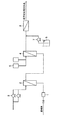
図1は、本発明の電子材料用洗浄水の製造工程の一態様の工程系統図である。超純水は、流量計1を経由して脱気膜装置2に送られる。脱気膜装置は、ガス透過膜を介して超純水と接する気相側が真空ポンプ3により減圧状態に保たれ、超純水中に溶存しているガス分が除去される。脱気された超純水は、次いで溶解膜装置4に送られる。溶解膜装置においては、水素供給器5から供給された水素ガスが気相側に送られ、ガス透過膜を介して超純水に供給される。溶存水素濃度が所定の値に達した超純水には、薬液貯槽6から薬注ポンプ7によりアンモニア水などの薬液が供給され、所定のpH値に調整される。水素を溶解し、アルカリ性となった超純水は、最後に精密ろ過装置8に送られ、MFフィルターなどにより微粒子を除去して本発明の電子材料用洗浄水が得られる。
【0006】
本発明において、超純水の脱気及び水素ガスの供給に用いるガス透過膜には特に制限はなく、例えば、ポリプロピレン、ポリジメチルシロキサン、ポリカーボネート−ポリジメチルシロキサンブロック共重合体、ポリビニルフェノール−ポリジメチルシロキサン−ポリスルホンブロック共重合体、ポリ(4−メチルペンテン−1)、ポリ(2,6−ジメチルフェニレンオキシド)、ポリテトラフルオロエチレンなどの高分子膜などを挙げることができる。水素ガスの供給方法には特に制限はなく、例えば、重質油のガス化反応により得られる合成ガスからの分離、メタノールの接触分解や水蒸気改質、水の電気分解などを挙げることができる。もちろん、高純度水素ガスボンベを使用してもよい。ガス透過膜の液体側に脱気した超純水を通過させ、気体側に水素ガスを供給することにより、水素ガスはガス透過膜を経由して超純水中に移行する。
本発明の電子材料用洗浄水は、溶存水素濃度が0.7mg/リットル以上飽和濃度以下である。水素ガスの水への飽和溶解度は、水素ガスと水蒸気の分圧の合計が760mmHgのとき、10℃においては1.7mg/リットル、20℃においては1.6mg/リットル、30℃においては1.5mg/リットル、40℃においては1.4mg/リットルである。電子材料用洗浄水中の溶存水素濃度が0.7mg/リットル未満であると、微粒子で汚染された電子材料からの微粒子の除去が不十分となるおそれがある。
【0007】
本発明の電子材料用洗浄水は、pHが8〜12である。電子材料用洗浄水のpH調整のために添加するアルカリには特に制限はないが、アンモニア水を特に好適に使用することができる。電子材料用洗浄水のpHが6未満であると、微粒子で汚染された電子材料からの微粒子の除去が不十分となるおそれがある。電子材料用洗浄水のpHが12を超えると、洗浄後のすすぎ工程に多量の超純水と長時間を要する上に、廃液の中和に必要な酸の量が多くなる。
本発明の電子材料用洗浄水を、微粒子で汚染された電子材料と接触させる方法には特に制限はなく、微粒子の種類、粒度、付着量などに応じて適宜選択することができる。例えば、微粒子で汚染された電子材料を電子材料用洗浄水に浸漬してバッチ洗浄することができ、あるいは、1枚ずつ処理する枚葉式洗浄を行うこともできる。枚葉式洗浄の方法としては、微粒子で汚染された電子材料を回転させつつ電子材料用洗浄水を流しかけるスピン洗浄などが挙げられる。
本発明においては、微粒子で汚染された電子材料の洗浄に際して、電子材料用洗浄水に超音波を照射する。電子材料用洗浄水に超音波を照射する方法には特に制限はなく、例えば、バッチ洗浄においては、電子材料用洗浄水を貯留した槽に超音波の振動を伝達することができ、スピン洗浄においては、流しかける電子材料用洗浄水のノズル部において、超音波の振動を伝達することができる。照射する超音波の周波数は、20kHz以上であることが好ましく、400kHz以上であることがより好ましい。超音波の周波数が20kHz未満であると、微粒子で汚染された電子材料からの微粒子の除去が不十分となるおそれがある。被洗浄物表面に損傷を与えない精密洗浄を行うには、400kHz以上の、特に高周波の超音波が望ましい。
【0008】
本発明によれば、微粒子で汚染された電子材料の洗浄に使用する薬品の量を大幅に減少し、かつ高い洗浄効果を得ることができ、さらに、電子材料の洗浄後の廃液処理が容易になる。すなわち、従来の洗浄廃液は、アンモニアや過酸化水素を大量に含んだ高濃度の状態で排出されるため、中和処理や分解処理が必要であり、廃液処理においても洗浄液の調製に使用したのと同程度の量の薬品が必要となる。本発明においては、排出されるのはアルカリを含んだpH8〜12の液であり、例えば、少量の酸を加えて中和することにより放流し得る水質となる。もちろん、超純水の原水として再利用することもできる水質である。廃液中に含まれる水素ガスは微量であり、通常は安全上の問題を生ずることはないが、使用環境によっては、必要に応じて廃液中に溶存する水素ガスを分解することができる。例えば、溶存水素を含有した水に空気吹き込みなどによって酸素を溶解し、パラジウム触媒などの存在下において、水素と酸素の反応により水を生成して、溶存水素を除去することができる。
【0009】
【実施例】
以下に、実施例を挙げて本発明をさらに詳細に説明するが、本発明はこれらの実施例によりなんら限定されるものではない。
実施例1(電子材料用洗浄水の製造)
図1に示す装置を用いて、電子材料用洗浄水を製造した。脱気膜装置、溶解膜装置ともに、ポリプロピレン製のガス透過膜を備えたものであり、脱気膜装置の気相側は真空ポンプにより50Torr以下の減圧とし、溶解膜装置の気相側には水素ガスを1kg/cm2(ゲージ圧)の圧力で供給した。この装置に、超純水を700ml/分で供給し、薬注ポンプから希釈したアンモニア水を3.5ml/分で供給した。精密ろ過装置から流出する電子材料用洗浄水は、溶存水素濃度が1.42mg/リットルであり、pHは10.6であった。
比較例1
図1に示す装置の配管を変更し、超純水を脱気膜装置で脱気することなく、直接溶解膜装置へ送りこんだ以外は、実施例1と同じ操作を繰り返した。精密ろ過装置から流出する電子材料用洗浄水は、溶存水素濃度が0.63mg/リットルであり、pHは10.6であった。
実施例1と比較例1の結果から、超純水を脱気したのち、ガス透過膜を介して水素ガスを供給することにより、溶存水素濃度を0.7mg/リットル以上とし得ることが分かる。
比較例2
50A、4.5Vで、流速が3.5リットル/分の条件で調製した電解カソード水中の溶存水素濃度を測定したところ、0.55mg/リットルであった。この結果から、電気分解によっては、溶存水素濃度を0.7mg/リットル以上とすることは困難であることが分かる。
実施例2(シリコンウェーハの洗浄)
オゾンを含有する超純水で表面を酸化した直径6インチのシリコンウェーハを、アルミナ微粉末で汚染することにより、表面にアルミナの微粒子が付着した汚染ウェーハを作製した。この汚染ウェーハについて、レーザー散乱光検出方式にもとづくウェーハ・ゴミ検出装置[東京光学機械(株)]により付着微粒子数を測定したところ、ウェーハ1枚当たり、直径0.2〜0.5μmの微粒子が12,600個、直径0.5〜1.0μmの微粒子が31,200個、直径1.0μm以上の微粒子が200個、合計44,000個であった。
この汚染ウェーハを500rpmで回転させ、実施例1の精密ろ過装置より流出する溶存水素濃度1.42mg/リットル、pH10.6の電子材料用洗浄水に、超音波照射ノズル[プレテック社、Fine Jet]を用いて周波数1.6MHzの超音波を出力13.5W/cm2で照射しつつ、700ml/分で流しかけ、60秒間スピン洗浄を行った。次いで、超純水を用いてすすぎを行ったのち乾燥した。
乾燥後のウェーハ表面の付着微粒子数を、同様にして測定したところ、ウェーハ1枚当たり、直径0.2〜0.5μmの微粒子が400個、直径0.5〜1.0μmの微粒子が300個、直径1.0μm以上の微粒子が10個、合計710個であり、ウェーハ表面の微粒子の除去率は98.4%であった。
比較例3
実施例1で得られる電子材料用洗浄水の代わりに、比較例2で得られる電解カソード水にアンモニア水を添加してpHを10.6に調整した液を洗浄水として用いた以外は、実施例2と同じ操作を繰り返した。
洗浄、乾燥後のウェーハ表面の付着微粒子数は、ウェーハ1枚当たり、直径0.2〜0.5μmの微粒子が2,100個、直径0.5〜1.0μmの微粒子が1,400個、直径1.0μm以上の微粒子が10個、合計3,510個であり、ウェーハ表面の微粒子の除去率は92.0%であった。
比較例4
実施例1で得られる電子材料用洗浄水の代わりに、超純水にアンモニア水を添加してpHを10.6に調整した液を洗浄水として用い、洗浄時間を3分間とした以外は、実施例2と同じ操作を繰り返した。
洗浄、乾燥後のウェーハ表面の付着微粒子数は、ウェーハ1枚当たり7,900個であり、ウェーハ表面の微粒子の除去率は82.0%であった。
比較例5
実施例1で得られる電子材料用洗浄水の代わりに、超純水をそのまま洗浄水として用い、洗浄時間を3分間とした以外は、実施例2と同じ操作を繰り返した。
洗浄、乾燥後のウェーハ表面の付着微粒子数は、ウェーハ1枚当たり35,400個であり、ウェーハ表面の微粒子の除去率は19.5%であった。
実施例2及び比較例3〜5の結果を第1表に示す。
【0010】
【表1】

第1表の結果から、本発明の電子材料用洗浄水を用いて洗浄した汚染ウェーハからは、アルミナの微粒子が高い除去率で洗浄、除去されているが、電解カソード水にアンモニア水を加えてアルカリ性にした洗浄水及び超純水にアンモニア水を加えてアルカリ性にした洗浄水を用いた場合は、微粒子の除去率が低く、単に超純水をそのまま洗浄水として用いた場合は、除去率が極端に低くなることが分かる。
実施例3(シリコンウェーハの洗浄)
スピン洗浄時間を30秒間及び3分間とした以外は、実施例2と同じ操作を繰り返した。
洗浄、乾燥後のウェーハ表面の付着微粒子数及び微粒子の除去率は、洗浄時間30秒間のとき、それぞれ1,400個、96.8%であり、洗浄時間3分のとき、それぞれ200個、99.5%であった。
比較例6
スピン洗浄時間を30秒間及び3分間とした以外は、比較例3と同じ操作を繰り返した。
洗浄、乾燥後のウェーハ表面の付着微粒子数及び微粒子の除去率は、洗浄時間30秒間のとき、それぞれ7,900個、82.0%であり、洗浄時間3分のとき、それぞれ3,100個、93.0%であった。
実施例3及び比較例6の結果に実施例2及び比較例3の結果を合わせて、洗浄時間と付着微粒子数及び微粒子の除去率の関係を第2表に示す。
【0012】
【表2】
第2表の結果から、本発明の電子材料用洗浄水を用いて洗浄した汚染ウェーハからは、3分間の洗浄により、アルミナの微粒子はほぼ完全に除去されているが、電解カソード水にアンモニア水を加えてアルカリ性にした洗浄水を用いた場合は、微粒子の除去率が低く、しかも除去率が頭打ちになる傾向があり、洗浄時間を延長しても微粒子の完全な除去は困難であろうと推定される。
【0014】
【発明の効果】
本発明の電子材料用洗浄水は、使用する薬剤の量が少なく、容易に製造することができ、微粒子で汚染された電子材料の表面を高い洗浄効率で洗浄して微粒子を除去することができ、さらに発生する廃液を容易に処理することができる。
【図面の簡単な説明】
【図1】図1は、本発明の電子材料用洗浄水の製造工程の一態様の工程系統図である。
【符号の説明】
1 流量計
2 脱気膜装置
3 真空ポンプ
4 溶解膜装置
5 水素供給器
6 薬液貯槽
7 薬注ポンプ
8 精密ろ過装置[0001]
BACKGROUND OF THE INVENTION
The present invention relates to cleaning water for electronic materials. More specifically, the present invention relates to an electronic material such as a semiconductor silicon substrate or a liquid crystal glass substrate contaminated with fine particles, which uses a small amount of chemicals, uses ultrasonic waves, and has a high contaminant removal rate. It is related with the washing water for electronic materials which can be washed with.
[0002]
[Prior art]
Conventionally, cleaning of the semiconductor surface and the like in the LSI manufacturing process is mainly performed by immersing the semiconductor in a solution prepared by mixing concentrated ammonia water or concentrated hydrochloric acid, hydrogen peroxide water and ultrapure water, and then rinsing with ultrapure water. The so-called RCA cleaning method has been performed. The RCA cleaning method is an effective method for removing the metal content on the semiconductor surface, but at the same time, the fine particles adhering to the semiconductor surface are also removed. However, in such a method, a large amount of high-concentration acid, alkali or hydrogen peroxide is used, so that these chemicals are discharged into the waste liquid, and there is a great burden on neutralization and precipitation in waste water treatment. At the same time, a large amount of sludge is generated. That is, in order to ensure the cleanliness of the surface of the semiconductor substrate, a large amount of cost is required for the chemical and waste liquid treatment. For this reason, the washing | cleaning method which can reduce the chemical usage-amount without reducing washing | cleaning efficiency was calculated | required.
[0003]
[Problems to be solved by the invention]
The present invention is an electronic material cleaning that can clean an electronic material such as a silicon substrate for a semiconductor and a glass substrate for a liquid crystal contaminated by fine particles with a small amount of chemicals used and with a high contaminant removal rate. It was made for the purpose of providing water.
[0004]
[Means for Solving the Problems]
As a result of intensive studies to solve the above problems, the present inventors have found that alkaline ultrapure water in which hydrogen gas is dissolved is extremely effective for cleaning electronic materials contaminated with fine particles, The present invention has been completed based on this finding.
That is, the present invention
(1) Ultrapure water is degassed, hydrogen gas is supplied through a gas permeable membrane, alkali is added, and further, it is sent to a microfiltration device to remove fine particles, so that the dissolved hydrogen concentration is reduced to 0. Manufacturing of cleaning water for electronic materials, characterized in that it provides cleaning water for cleaning electronic materials contaminated with fine particles made of ultrapure water having a pH of 8 to 12 but not less than 7 mg / liter. Method and
( 2 ) A method for cleaning an electronic material, characterized in that an electronic material contaminated with fine particles is brought into contact with the electronic material cleaning water described in (1) while irradiating ultrasonic waves.
Is to provide.
[0005]
DETAILED DESCRIPTION OF THE INVENTION
Electronic materials cleaning water of the present invention, the dissolved hydrogen concentration is below the saturation concentration or more 0.7 mg / liter, a wash water pH is from ultrapure water is 8-12. Examples of the electronic material that can be cleaned with the cleaning water for electronic materials of the present invention include a silicon substrate for semiconductor, a glass substrate for liquid crystal, a precision electronic component, and parts of these manufacturing apparatuses.
There is no restriction | limiting in particular in the manufacturing method of the ultrapure water used for this invention, For example, primary pure water, such as deionized water and distilled water, is processed using a reverse osmosis membrane, an ultrafiltration membrane, a microfiltration membrane, etc. Can be obtained. The ultrapure water used in the present invention preferably has an electrical resistivity at 25 ° C. of 18 MΩ · cm or more, organic carbon of 10 μg / liter or less, and fine particles of 10,000 pieces / liter or less.
FIG. 1 is a process flow diagram of one embodiment of a process for producing electronic material cleaning water according to the present invention. The ultrapure water is sent to the degassing
[0006]
In the present invention, the gas permeable membrane used for degassing ultrapure water and supplying hydrogen gas is not particularly limited, and examples thereof include polypropylene, polydimethylsiloxane, polycarbonate-polydimethylsiloxane block copolymer, and polyvinylphenol-polydimethyl. Examples thereof include siloxane-polysulfone block copolymers, polymer films such as poly (4-methylpentene-1), poly (2,6-dimethylphenylene oxide), and polytetrafluoroethylene. The method for supplying hydrogen gas is not particularly limited, and examples thereof include separation from synthesis gas obtained by gasification reaction of heavy oil, catalytic cracking or steam reforming of methanol, and water electrolysis. Of course, a high purity hydrogen gas cylinder may be used. By passing degassed ultrapure water to the liquid side of the gas permeable membrane and supplying hydrogen gas to the gas side, the hydrogen gas is transferred to the ultrapure water through the gas permeable membrane.
The cleaning water for electronic material of the present invention has a dissolved hydrogen concentration of 0.7 mg / liter or more and a saturation concentration or less. The saturated solubility of hydrogen gas in water is 1.7 mg / liter at 10 ° C., 1.6 mg / liter at 20 ° C., and 1.30 mg at 30 ° C. when the total partial pressure of hydrogen gas and water vapor is 760 mmHg. 5 mg / liter and 1.4 mg / liter at 40 ° C. If the dissolved hydrogen concentration in the cleaning water for electronic materials is less than 0.7 mg / liter, removal of the fine particles from the electronic material contaminated with the fine particles may be insufficient.
[0007]
Electronic material cleaning water of this invention, pH is 8-12. Although there is no restriction | limiting in particular in the alkali added for pH adjustment of the washing water for electronic materials, Ammonia water can be used especially suitably. When the pH of the cleaning water for electronic materials is less than 6, there is a risk that the removal of the fine particles from the electronic material contaminated with the fine particles may be insufficient. If the pH of the cleaning water for electronic materials exceeds 12, a large amount of ultrapure water and a long time are required for the rinsing process after cleaning, and the amount of acid necessary for neutralizing the waste liquid increases.
The method for bringing the electronic material cleaning water of the present invention into contact with the electronic material contaminated with fine particles is not particularly limited, and can be appropriately selected according to the type, particle size, adhesion amount, and the like of the fine particles. For example, an electronic material contaminated with fine particles can be immersed in electronic material cleaning water for batch cleaning, or single wafer cleaning can be performed one by one. The single wafer cleaning method includes spin cleaning in which electronic material cleaning water is poured while rotating the electronic material contaminated with fine particles.
In the present invention, when cleaning the electronic material contaminated with the fine particles, the electronic material cleaning water is irradiated with ultrasonic waves. There is no particular limitation on the method of irradiating the cleaning water for electronic materials with ultrasonic waves. For example, in batch cleaning, ultrasonic vibration can be transmitted to a tank storing the cleaning water for electronic materials. Can transmit ultrasonic vibrations in the nozzle portion of the cleaning water for electronic material to be poured. The frequency of the ultrasonic wave to be irradiated is preferably 20 kHz or more, and more preferably 400 kHz or more. If the frequency of the ultrasonic wave is less than 20 kHz, removal of the fine particles from the electronic material contaminated with the fine particles may be insufficient. In order to perform precision cleaning without damaging the surface of the object to be cleaned, ultrasonic waves of 400 kHz or higher, particularly high frequency are desirable.
[0008]
According to the present invention, the amount of chemicals used for cleaning electronic materials contaminated with fine particles can be greatly reduced, and a high cleaning effect can be obtained. Further, waste liquid treatment after cleaning of electronic materials can be easily performed. Become. In other words, the conventional cleaning waste liquid is discharged in a high concentration state containing a large amount of ammonia and hydrogen peroxide, so neutralization treatment and decomposition treatment are necessary, and it was also used for cleaning liquid preparation in waste liquid treatment. The same amount of chemical is required. In the present invention, the discharged solution is a solution having a pH of 8 to 12 containing alkali. For example, the solution can be discharged by adding a small amount of acid to neutralize it. Of course, the water quality can be reused as the raw water of ultrapure water. The amount of hydrogen gas contained in the waste liquid is very small and usually does not cause a safety problem. However, depending on the use environment, the hydrogen gas dissolved in the waste liquid can be decomposed as necessary. For example, dissolved hydrogen can be removed by dissolving oxygen by blowing air into water containing dissolved hydrogen and generating water by the reaction of hydrogen and oxygen in the presence of a palladium catalyst or the like.
[0009]
【Example】
Hereinafter, the present invention will be described in more detail with reference to examples, but the present invention is not limited to these examples.
Example 1 (Manufacture of cleaning water for electronic materials)
Washing water for electronic materials was manufactured using the apparatus shown in FIG. Both the degassing membrane device and the dissolving membrane device are equipped with a gas permeable membrane made of polypropylene. The gas phase side of the degassing membrane device is reduced to 50 Torr or less by a vacuum pump, and the gas phase side of the dissolving membrane device is Hydrogen gas was supplied at a pressure of 1 kg / cm 2 (gauge pressure). Ultrapure water was supplied to this apparatus at 700 ml / min, and diluted ammonia water was supplied from the chemical injection pump at 3.5 ml / min. The washing water for electronic materials flowing out from the microfiltration device had a dissolved hydrogen concentration of 1.42 mg / liter and a pH of 10.6.
Comparative Example 1
The same operation as in Example 1 was repeated except that the piping of the apparatus shown in FIG. 1 was changed and ultrapure water was sent directly to the dissolution membrane apparatus without deaeration with the deaeration membrane apparatus. The electronic material washing water flowing out from the microfiltration apparatus had a dissolved hydrogen concentration of 0.63 mg / liter and a pH of 10.6.
From the results of Example 1 and Comparative Example 1, it is understood that the dissolved hydrogen concentration can be increased to 0.7 mg / liter or more by supplying hydrogen gas through the gas permeable membrane after degassing ultrapure water.
Comparative Example 2
The dissolved hydrogen concentration in the electrolytic cathode water prepared under the conditions of 50 A, 4.5 V, and a flow rate of 3.5 liters / minute was 0.55 mg / liter. From this result, it can be seen that it is difficult to increase the dissolved hydrogen concentration to 0.7 mg / liter or more by electrolysis.
Example 2 (Silicon wafer cleaning)
A silicon wafer having a diameter of 6 inches whose surface was oxidized with ultrapure water containing ozone was contaminated with fine alumina powder to produce a contaminated wafer having fine alumina particles adhered to the surface. With respect to this contaminated wafer, when the number of adhering fine particles was measured by a wafer / dust detection device [Tokyo Optical Machinery Co., Ltd.] based on a laser scattered light detection method, fine particles having a diameter of 0.2 to 0.5 μm per wafer were obtained. There were 12,600 fine particles with a diameter of 0.5 to 1.0 μm, 31,200 fine particles, and 200 fine particles with a diameter of 1.0 μm or more, for a total of 44,000.
This contaminated wafer is rotated at 500 rpm, and an ultrasonic irradiation nozzle [Pretech, Fine Jet] is used for cleaning water for electronic materials having a dissolved hydrogen concentration of 1.42 mg / liter and a pH of 10.6 flowing out from the microfiltration apparatus of Example 1. While irradiating an ultrasonic wave with a frequency of 1.6 MHz with an output of 13.5 W / cm 2, it was applied at 700 ml / min and spin washed for 60 seconds. Subsequently, after rinsing using ultrapure water, it was dried.
The number of adhering fine particles on the wafer surface after drying was measured in the same manner. As a result, 400 fine particles having a diameter of 0.2 to 0.5 μm and 300 fine particles having a diameter of 0.5 to 1.0 μm per wafer. The number of fine particles having a diameter of 1.0 μm or more was 10 for a total of 710, and the removal rate of fine particles on the wafer surface was 98.4%.
Comparative Example 3
Instead of the electronic material cleaning water obtained in Example 1, a solution prepared by adding ammonia water to the electrolytic cathode water obtained in Comparative Example 2 to adjust the pH to 10.6 was used as the cleaning water. The same operation as in Example 2 was repeated.
The number of adhering fine particles on the wafer surface after cleaning and drying is 2,100 fine particles having a diameter of 0.2 to 0.5 μm and 1,400 fine particles having a diameter of 0.5 to 1.0 μm per wafer. The number of fine particles having a diameter of 1.0 μm or more was 10 in total, 3,510, and the removal rate of fine particles on the wafer surface was 92.0%.
Comparative Example 4
Instead of the cleaning water for electronic materials obtained in Example 1, a solution prepared by adding ammonia water to ultrapure water and adjusting the pH to 10.6 was used as the cleaning water, and the cleaning time was 3 minutes. The same operation as in Example 2 was repeated.
The number of adhered fine particles on the wafer surface after cleaning and drying was 7,900 per wafer, and the removal rate of fine particles on the wafer surface was 82.0%.
Comparative Example 5
The same operation as in Example 2 was repeated except that ultrapure water was directly used as the cleaning water instead of the electronic material cleaning water obtained in Example 1, and the cleaning time was 3 minutes.
The number of fine particles adhered on the wafer surface after cleaning and drying was 35,400 per wafer, and the removal rate of fine particles on the wafer surface was 19.5%.
The results of Example 2 and Comparative Examples 3 to 5 are shown in Table 1.
[0010]
[Table 1]
From the results shown in Table 1, fine particles of alumina are cleaned and removed from the contaminated wafer cleaned using the cleaning water for electronic materials according to the present invention, but ammonia water is added to the electrolytic cathode water. When using alkaline cleaning water and cleaning water made by adding ammonia water to ultrapure water, the removal rate of fine particles is low, and when ultrapure water is simply used as cleaning water, the removal rate is low. It turns out that it becomes extremely low.
Example 3 (Silicon wafer cleaning)
The same operation as in Example 2 was repeated except that the spin cleaning time was 30 seconds and 3 minutes.
The number of adhered particles on the wafer surface after cleaning and drying and the removal rate of the particles are 1,400 and 96.8% when the cleaning time is 30 seconds, respectively, and 200 and 99 when the cleaning time is 3 minutes, respectively. It was 5%.
Comparative Example 6
The same operation as Comparative Example 3 was repeated except that the spin cleaning time was 30 seconds and 3 minutes.
The number of adhering fine particles and the removal rate of fine particles on the wafer surface after cleaning and drying are 7,900 and 82.0% when the cleaning time is 30 seconds, respectively, and 3,100 when the cleaning time is 3 minutes. 93.0%.
The results of Example 3 and Comparative Example 6 are combined with the results of Example 2 and Comparative Example 3, and the relationship between the cleaning time, the number of attached fine particles and the removal rate of the fine particles is shown in Table 2.
[0012]
[Table 2]
From the results shown in Table 2, fine particles of alumina were almost completely removed from the contaminated wafer cleaned with the electronic material cleaning water of the present invention by cleaning for 3 minutes. It is estimated that the removal rate of fine particles is low and the removal rate tends to reach a peak when washing water is made alkaline by adding water, and it is difficult to completely remove fine particles even if the washing time is extended. Is done.
[0014]
【The invention's effect】
The cleaning water for electronic materials of the present invention uses a small amount of chemicals and can be easily manufactured, and can clean the surface of the electronic material contaminated with fine particles with high cleaning efficiency to remove the fine particles. Further, the generated waste liquid can be easily treated.
[Brief description of the drawings]
FIG. 1 is a process flow diagram of one embodiment of a process for producing cleaning water for electronic materials according to the present invention.
[Explanation of symbols]
DESCRIPTION OF SYMBOLS 1
Claims (2)
Priority Applications (1)
| Application Number | Priority Date | Filing Date | Title |
|---|---|---|---|
| JP19778297A JP3940967B2 (en) | 1997-07-08 | 1997-07-08 | Method for producing cleaning water for electronic material and method for cleaning electronic material |
Applications Claiming Priority (1)
| Application Number | Priority Date | Filing Date | Title |
|---|---|---|---|
| JP19778297A JP3940967B2 (en) | 1997-07-08 | 1997-07-08 | Method for producing cleaning water for electronic material and method for cleaning electronic material |
Publications (2)
| Publication Number | Publication Date |
|---|---|
| JPH1129794A JPH1129794A (en) | 1999-02-02 |
| JP3940967B2 true JP3940967B2 (en) | 2007-07-04 |
Family
ID=16380269
Family Applications (1)
| Application Number | Title | Priority Date | Filing Date |
|---|---|---|---|
| JP19778297A Expired - Fee Related JP3940967B2 (en) | 1997-07-08 | 1997-07-08 | Method for producing cleaning water for electronic material and method for cleaning electronic material |
Country Status (1)
| Country | Link |
|---|---|
| JP (1) | JP3940967B2 (en) |
Cited By (1)
| Publication number | Priority date | Publication date | Assignee | Title |
|---|---|---|---|---|
| KR101255895B1 (en) * | 2009-12-10 | 2013-04-17 | 가부시키가이샤 코아테크노로지 | Method for manufacturing nano-bubble water containing saturated gas |
Families Citing this family (9)
| Publication number | Priority date | Publication date | Assignee | Title |
|---|---|---|---|---|
| JP4506909B2 (en) * | 1999-02-17 | 2010-07-21 | 栗田工業株式会社 | Planarization processing method of silicon substrate surface oxide film |
| TW464970B (en) | 1999-04-21 | 2001-11-21 | Sharp Kk | Ultrasonic cleaning device and resist-stripping device |
| JP4484980B2 (en) | 1999-05-20 | 2010-06-16 | 株式会社ルネサステクノロジ | Photomask cleaning method, cleaning apparatus, and photomask cleaning liquid |
| JP4683314B2 (en) * | 2000-08-01 | 2011-05-18 | 栗田工業株式会社 | Cleaning method for silicon substrate for semiconductor |
| CN1444259A (en) | 2002-03-12 | 2003-09-24 | 株式会社东芝 | Method for mfg. semiconductor device |
| JP4967001B2 (en) * | 2009-03-13 | 2012-07-04 | ミズ株式会社 | Method for producing hydrogen-containing biological fluid and apparatus therefor |
| JP5353730B2 (en) * | 2010-01-25 | 2013-11-27 | 信越半導体株式会社 | Ultrasonic cleaning method, ultrasonic cleaning apparatus, and method for producing propagation water used for ultrasonic cleaning |
| JP5266267B2 (en) * | 2010-02-26 | 2013-08-21 | ミズ株式会社 | Method and apparatus for producing hydrogen-containing biological fluid |
| JP6154860B2 (en) * | 2015-07-17 | 2017-06-28 | 野村マイクロ・サイエンス株式会社 | Method and apparatus for producing hydrogen water for cleaning |
-
1997
- 1997-07-08 JP JP19778297A patent/JP3940967B2/en not_active Expired - Fee Related
Cited By (1)
| Publication number | Priority date | Publication date | Assignee | Title |
|---|---|---|---|---|
| KR101255895B1 (en) * | 2009-12-10 | 2013-04-17 | 가부시키가이샤 코아테크노로지 | Method for manufacturing nano-bubble water containing saturated gas |
Also Published As
| Publication number | Publication date |
|---|---|
| JPH1129794A (en) | 1999-02-02 |
Similar Documents
| Publication | Publication Date | Title |
|---|---|---|
| JP3409849B2 (en) | Manufacturing equipment for cleaning liquid for cleaning electronic components | |
| US9129797B2 (en) | Cleaning method | |
| US5783790A (en) | Wet treatment method | |
| JP4157185B2 (en) | Cleaning liquid and cleaning method | |
| KR100453415B1 (en) | Cleaning solution and cleaning method | |
| WO2009128327A1 (en) | Cleaning water for electronic material, method of cleaning electronic material, and system for supplying water containing dissolved gases | |
| JPH08187474A (en) | Washing method | |
| JP3296405B2 (en) | Cleaning method and cleaning device for electronic component members | |
| JP3940967B2 (en) | Method for producing cleaning water for electronic material and method for cleaning electronic material | |
| JP2012143708A (en) | Washing method | |
| JP4482844B2 (en) | Wafer cleaning method | |
| JP4273440B2 (en) | Cleaning water for electronic material and cleaning method for electronic material | |
| JPH1022246A (en) | Cleaning method | |
| JP3332323B2 (en) | Cleaning method and cleaning device for electronic component members | |
| JP3296407B2 (en) | Cleaning method and cleaning device for electronic component members | |
| JP3639102B2 (en) | Wet processing equipment | |
| JP2005150768A (en) | Cleaning method and cleaning method of electronic component | |
| JP2010135810A (en) | METHOD OF CONTROLLING pH VALUE OF SOLUTION AND OXIDATION-REDUCTION POTENTIAL, AND APPARATUS | |
| JP3507588B2 (en) | Wet processing method and processing apparatus | |
| JP2000288495A (en) | Cleaning method | |
| JP2004296463A (en) | Cleaning method and cleaning device | |
| JP3507590B2 (en) | Wet processing method and processing apparatus | |
| JP2002001243A (en) | Method for cleaning electronic material | |
| JPH1071375A (en) | Washing method | |
| JP2000279902A (en) | Method of washing substrate |
Legal Events
| Date | Code | Title | Description |
|---|---|---|---|
| A521 | Written amendment |
Free format text: JAPANESE INTERMEDIATE CODE: A523 Effective date: 20040520 |
|
| A621 | Written request for application examination |
Free format text: JAPANESE INTERMEDIATE CODE: A621 Effective date: 20040520 |
|
| A977 | Report on retrieval |
Free format text: JAPANESE INTERMEDIATE CODE: A971007 Effective date: 20050815 |
|
| A131 | Notification of reasons for refusal |
Free format text: JAPANESE INTERMEDIATE CODE: A131 Effective date: 20050830 |
|
| A521 | Written amendment |
Free format text: JAPANESE INTERMEDIATE CODE: A523 Effective date: 20051021 |
|
| A131 | Notification of reasons for refusal |
Free format text: JAPANESE INTERMEDIATE CODE: A131 Effective date: 20051208 |
|
| TRDD | Decision of grant or rejection written | ||
| A01 | Written decision to grant a patent or to grant a registration (utility model) |
Free format text: JAPANESE INTERMEDIATE CODE: A01 Effective date: 20070309 |
|
| A61 | First payment of annual fees (during grant procedure) |
Free format text: JAPANESE INTERMEDIATE CODE: A61 Effective date: 20070322 |
|
| R150 | Certificate of patent or registration of utility model |
Free format text: JAPANESE INTERMEDIATE CODE: R150 |
|
| FPAY | Renewal fee payment (event date is renewal date of database) |
Free format text: PAYMENT UNTIL: 20100413 Year of fee payment: 3 |
|
| FPAY | Renewal fee payment (event date is renewal date of database) |
Free format text: PAYMENT UNTIL: 20110413 Year of fee payment: 4 |
|
| FPAY | Renewal fee payment (event date is renewal date of database) |
Free format text: PAYMENT UNTIL: 20120413 Year of fee payment: 5 |
|
| FPAY | Renewal fee payment (event date is renewal date of database) |
Free format text: PAYMENT UNTIL: 20130413 Year of fee payment: 6 |
|
| FPAY | Renewal fee payment (event date is renewal date of database) |
Free format text: PAYMENT UNTIL: 20140413 Year of fee payment: 7 |
|
| LAPS | Cancellation because of no payment of annual fees |