JP3931925B2 - Color filter printing apparatus and printing method - Google Patents
Color filter printing apparatus and printing method Download PDFInfo
- Publication number
- JP3931925B2 JP3931925B2 JP52285996A JP52285996A JP3931925B2 JP 3931925 B2 JP3931925 B2 JP 3931925B2 JP 52285996 A JP52285996 A JP 52285996A JP 52285996 A JP52285996 A JP 52285996A JP 3931925 B2 JP3931925 B2 JP 3931925B2
- Authority
- JP
- Japan
- Prior art keywords
- pattern
- ink
- transfer layer
- black matrix
- roll
- Prior art date
- Legal status (The legal status is an assumption and is not a legal conclusion. Google has not performed a legal analysis and makes no representation as to the accuracy of the status listed.)
- Expired - Fee Related
Links
Images


Classifications
-
- G—PHYSICS
- G02—OPTICS
- G02B—OPTICAL ELEMENTS, SYSTEMS OR APPARATUS
- G02B5/00—Optical elements other than lenses
- G02B5/20—Filters
- G02B5/201—Filters in the form of arrays
-
- B—PERFORMING OPERATIONS; TRANSPORTING
- B41—PRINTING; LINING MACHINES; TYPEWRITERS; STAMPS
- B41M—PRINTING, DUPLICATING, MARKING, OR COPYING PROCESSES; COLOUR PRINTING
- B41M1/00—Inking and printing with a printer's forme
- B41M1/10—Intaglio printing ; Gravure printing
-
- B—PERFORMING OPERATIONS; TRANSPORTING
- B41—PRINTING; LINING MACHINES; TYPEWRITERS; STAMPS
- B41M—PRINTING, DUPLICATING, MARKING, OR COPYING PROCESSES; COLOUR PRINTING
- B41M1/00—Inking and printing with a printer's forme
- B41M1/26—Printing on other surfaces than ordinary paper
- B41M1/34—Printing on other surfaces than ordinary paper on glass or ceramic surfaces
-
- B—PERFORMING OPERATIONS; TRANSPORTING
- B41—PRINTING; LINING MACHINES; TYPEWRITERS; STAMPS
- B41M—PRINTING, DUPLICATING, MARKING, OR COPYING PROCESSES; COLOUR PRINTING
- B41M3/00—Printing processes to produce particular kinds of printed work, e.g. patterns
- B41M3/003—Printing processes to produce particular kinds of printed work, e.g. patterns on optical devices, e.g. lens elements; for the production of optical devices
-
- B—PERFORMING OPERATIONS; TRANSPORTING
- B41—PRINTING; LINING MACHINES; TYPEWRITERS; STAMPS
- B41M—PRINTING, DUPLICATING, MARKING, OR COPYING PROCESSES; COLOUR PRINTING
- B41M1/00—Inking and printing with a printer's forme
- B41M1/14—Multicolour printing
-
- B—PERFORMING OPERATIONS; TRANSPORTING
- B41—PRINTING; LINING MACHINES; TYPEWRITERS; STAMPS
- B41M—PRINTING, DUPLICATING, MARKING, OR COPYING PROCESSES; COLOUR PRINTING
- B41M1/00—Inking and printing with a printer's forme
- B41M1/14—Multicolour printing
- B41M1/20—Multicolour printing by applying differently-coloured inks simultaneously to different parts of the printing surface
-
- B—PERFORMING OPERATIONS; TRANSPORTING
- B41—PRINTING; LINING MACHINES; TYPEWRITERS; STAMPS
- B41M—PRINTING, DUPLICATING, MARKING, OR COPYING PROCESSES; COLOUR PRINTING
- B41M7/00—After-treatment of prints, e.g. heating, irradiating, setting of the ink, protection of the printed stock
- B41M7/0081—After-treatment of prints, e.g. heating, irradiating, setting of the ink, protection of the printed stock using electromagnetic radiation or waves, e.g. ultraviolet radiation, electron beams
-
- G—PHYSICS
- G02—OPTICS
- G02F—OPTICAL DEVICES OR ARRANGEMENTS FOR THE CONTROL OF LIGHT BY MODIFICATION OF THE OPTICAL PROPERTIES OF THE MEDIA OF THE ELEMENTS INVOLVED THEREIN; NON-LINEAR OPTICS; FREQUENCY-CHANGING OF LIGHT; OPTICAL LOGIC ELEMENTS; OPTICAL ANALOGUE/DIGITAL CONVERTERS
- G02F1/00—Devices or arrangements for the control of the intensity, colour, phase, polarisation or direction of light arriving from an independent light source, e.g. switching, gating or modulating; Non-linear optics
- G02F1/01—Devices or arrangements for the control of the intensity, colour, phase, polarisation or direction of light arriving from an independent light source, e.g. switching, gating or modulating; Non-linear optics for the control of the intensity, phase, polarisation or colour
- G02F1/13—Devices or arrangements for the control of the intensity, colour, phase, polarisation or direction of light arriving from an independent light source, e.g. switching, gating or modulating; Non-linear optics for the control of the intensity, phase, polarisation or colour based on liquid crystals, e.g. single liquid crystal display cells
- G02F1/133—Constructional arrangements; Operation of liquid crystal cells; Circuit arrangements
- G02F1/1333—Constructional arrangements; Manufacturing methods
- G02F1/1335—Structural association of cells with optical devices, e.g. polarisers or reflectors
- G02F1/133509—Filters, e.g. light shielding masks
- G02F1/133514—Colour filters
- G02F1/133516—Methods for their manufacture, e.g. printing, electro-deposition or photolithography
Description
技術分野
本発明は液晶ディスプレイパネル用カラーフィルター、そのカラーフィルター用ブラックマトリックスパターン、およびそれらの製造方法に関するものである。
背景技術
液晶ディスプレイ(LCD)パネル、特にカラーLCDパネルはフラットスクリーンテレビ、投射テレビ、カムコーダテレビのファインダー等に使用されており、将来さらに様々な分野で使用されるものと期待されている。
能動マトリックス液晶ディスプレイの製造には複数の工程を要する。第1の工程では前面ガラスパネルが作成される。この工程では、ガラス等の適当な基板にカラーフィルターが設けられる。通常このカラーフィルターはブラックマトリックスパターンを形成し、3原色(レッド、グリーン、ブルー或いはイエロー、マゼンタ、シアン)のカラードットパターンないしカラーセルパターンをそのブラックマトリックスによって区画された領域内に形成することによって形成される。そのブラックマトリックスを形成する印刷された線は一般に幅約15〜25ミクロン、厚さ約0.5〜2ミクロンである。またレッド、グリーン、ブルーのカラーセルは一般に幅約70〜100ミクロン、長さ約200〜300ミクロン程度である。カラーセルは一般に約10ミクロン未満の厚さ、望ましくは、5ミクロン未満の厚さの薄膜状に印刷され、ブラックマトリックスによって形成されたパターン内に正しく位置され、均一に設けられなければならない。前面ガラス基板には通常さらに、平面化層、透明導電層およびポリイミド整列層がカラーフィルター上に設けられる。透明導電層は一般にインジウム酸化錫(ITO)で形成されるが、他の材料で形成してもよい。
第2の工程では、別の(後面)ガラスパネルを使用して薄膜トランジスタないし薄膜ダイオードおよび金属接続線が形成される。各トランジスタは液晶ディスプレイパネル内の各カラーピクセルのオンーオフスイッチとして機能する。最後の工程では両パネルを組み立てるとともに、その両パネル間に液晶材料を注入して液晶パネルを形成する。
カラーフィルターの製造で最も重要な工程の一つはブラックマトリックスパターンの作成である。ブラックマトリックスのエッジ鮮明度ないし鮮鋭度が特に重要である。カラーインクセルの場合と異なり、印刷の流れ等に起因するブラックマトリックスのエッジのばらつきは最終製品の検査の際に容易に見付けることができる。これに対してカラーピクセルのエッジは通常ブラックマトリックスパターンに隠されてしまう。したがってカラーピクセルのエッジのばらつきはブラックマトリックスによってある程度隠れるがブラックマトリックスのエッジのばらつきは隠すものがない。
ブラックマトリックスパターンは前記別のガラスパネル上の薄膜トランジスタを構成しているトランジスタと位置合わせをしなければならないため、カラードットパターンに比べて位置精度の要求がはるかに厳しい。これに対してブラックマトリックスパターンの幅がカラーピクセルの位置精度に若干の余裕を与える。すなわち、カラーピクセルを構成している個々のカラードットの間の領域がブラックマトリックスパターンを構成しているグリッドによって隠されるからである。典型的なブラックマトリックスパターンの一つは、互いに十文字に交差して、カラーセルピクセルのインクが中に配される長方形の領域を形成する細長い黒線のグリッドからなっている。このようなグリッドマトリックスは、液晶ディスプレイの反対側のガラスパネル上の薄膜トランジスタ(TFT)の位置に対応するグリッドセルのエッジに沿って配される黒色の小さい長方形をさらに備えている。位置精度の要求が厳しいために、一般的な長方形のサブピクセルグリッドパターンを有するブラックマトリックスパターンの場合には、ブラックマトリックスはカラーフィルターから見下ろした場合に先鋭で、鮮明なエッジだけが見えるように形成するのが望ましい。そのようなブラックマトリックスパターンを構成するグリッドの断面形状も直角なエッジを有する長方形である必要がある。またそのようなブラックマトリックスパターンの角および交差部も直角であって、カラーフィルターから見下ろしたときに直角なエッジのみが見える必要がある。今までは、カラーピクセルを構成するカラーインクドットを製造するのに使用することができる印刷技法がいくつかあったが、より細い、したがって解像力がより高い、ブラックマトリックスの線に対する要求には従来の印刷技術では応えることができなくなってしまった。この解像力の限界に近づくにつれて、印刷技法を使用して必要な鮮明度を維持するのは極めて困難になってくる。印刷技術における最大の問題は、インクの表面張力によってインクの断面が丸くなる傾向があり、そのためにエッジが不規則になることである。
したがって、例え、カラーフィルターパターンの他の部分は印刷技法で作成するにしても、ブラックマトリックスパターンは写真平版法によって作成するのが普通である。この写真平版法は多くの工程を必要とし、印刷技法に比べてはるかに複雑であり、しかもコストがはるかに高い。
カラーフィルターの製造におけるもう一つの重要な工程は、レッド、グリーン、ブルーのカラードット(カラーセルと言うこともある)の形成である。カラーセルはできる限り滑らかで厚みが均一となるように形成する必要がある。カラーフィルターパターンを印刷するのに従来使用されていた方法ではカラーパターンの滑らかさが不十分であった。これは主として従来のインクを付着させる方法ではインクセルの断面が丸くあるいは三角形になるからである。このため、カラーパターンの上に平面化層を形成して、付着方法に起因する滑らかさや厚みの均一性に関する欠陥を補正するのが普通である。またその透明な平面化層はITO層およびカラーパターン層へのイオンの移行と両層からのイオンの移行を防止するのにも役立つ。平面化層はできる限り滑らかにかつ平らに形成しなければならない。
平らな平面化層の形成を容易にするためには、カラーパターンが滑らかで、平らで、ガラス基板の下面にほぼ平らであるのが望ましい。カラーパターンの厚みが均一でないと透過光の強度が変動するため、ディスプレイのコントラストと色性能を良好にするためにはカラーパターンの厚みが均一であるのが望ましい。
本発明は解像力が高く、位置精度に優れた、高品質で厚みの均一なブラックマトリックスパターンおよびインクカラーフィルターアレイを従来技術のカラーフィルターアレイに比べて容易かつ低コストで提供することを目的とするものである。また本発明は従来の方法に比べて工程数の少ない方法で上記のようなブラックマトリックスパターンおよびインクカラーフィルターアレイを提供しようとするものである。
発明の開示
本発明によれば液晶ディスプレイ用のカラーフィルターの製造方法が提供される。本発明ではコレクターロール、コレクターパネル等のコレクター装置上に転写層が設けられる。その転写層上に隆起パターンが形成される。この隆起パターンは所望のブラックマトリックスパターンに対応しているのが望ましい。その転写層上の隆起パターンによって形成された凹部内にレッド、グリーン、ブルーのカラーセルが付着せしめられてカラーフィルターパターンが形成される。転写層上にカラーパターンを形成した後、この転写層とカラーフィルターパターンの複合材料全体をカラーフィルターパターンがガラス基板に接するようにしてガラス基板上に移す。この状態では転写層が一番上にあり、平面化層および保護層として作用する。転写層上の隆起パターンは印刷作業中およびその後にカラーセル間の離隔を維持するのに役立つ。
転写層上の隆起パターンは隆起したブラックマトリックスパターンとして形成するのが望ましい。この隆起ブラックマトリックスパターンはカラーインクセル間の離隔を維持するのに有用であるばかりでなく、鮮明度の高いブラックマトリックスパターンを形成するのに役立つ。隆起ブラックマトリックスパターンとは、転写層がコレクターの面上にあるとき、そのブラックマトリックスパターンの上面が転写層の上面より高いことを意味する。このブラックマトリックスパターンは厚み(転写層の他の部分からの高さ)が約1〜10ミクロンであるのが望ましく、約2〜6ミクロンであるのがより望ましく、3〜4ミクロンであるのが最も望ましい。
本発明の一実施の形態では、カラーフィルターの各ピクセルを構成するカラーセルを受け取る前に、転写層は所望のブラックマトリックスパターンに対応する凹部パターンを有するロールに接触せしめられる。これによって、所望のブラックマトリックスパターンに対応する隆起パターンが転写層上に形成される。必要ならば、その隆起パターンの頂面にブラックマトリックスインクを塗布して隆起ブラックマトリックスパターンを形成してもよい。
液晶ディスプレイパネルの他の部分にブラックマトリックスパターンを設けてもよい。例えば、薄膜トランジスタを担持するガラス基板のその薄膜トランジスタの上あるいは下に設けてもよい。この場合にはブラックマトリックスパターンはITO層の上に設けるのが望ましい。このような実施の形態では、前記隆起パターンはレッド、グリーン、ブルーのカラーセルを隔て、カラーセルをブラックマトリックスパターンと整合させるのに主として役立つ。隆起ブラックマトリックスパターンを形成するには、所望のブラックマトリックスパターンに対応する陰刻パターンを有する像ロール、像プレート等によって提供される凹版像面の凹部内にブラックマトリックスインクパターンを形成するのが望ましい。転写層に付着させる前あるいは付着させる間にブラックマトリックスインクを硬化、少なくとも半硬化させ、凹版の陰刻パターンが正確に複写されるようにするのが望ましい。凹版やグラビア印刷プレート内のインクは一般に負のメニスカスを有する。すなわち凹版の陰刻パターン内のインクの表面はプレート面の下方に湾曲する。したがって、転写層はブラックマトリックスインクと接触するときにはインクに付着できるように液体であるのが望ましい。この液体転写層はブラックマトリックスインクと接触している間に硬化され、凹版の陰刻パターン内からインクを取り出す。
隆起パターン(隆起ブラックマトリックスパターンであるのが望ましい)によって形成された凹部内にレッド、グリーン、ブルーのカラーセルを付着させるのにはインク印刷法が使用される。カラーセルを構成しているインクが変形可能なうちに、転写層、カラーインクセルからなる(ブラックマトリックスパターンを含むこともある)複合材料がガラス基板に移される。このようにして、軟らかい、変形可能なカラーインクセルが転写層とガラス基板の間で圧縮される。ガラス基板に移すときにカラーセルインクが塑性変形可能なため、レッド、グリーン、ブルーのインクセルはガラス基板に移す際に圧縮され、元々不均一な断面形状のインクセルが平らにのばされる。これによって、従来の技術で可能であったものに比べて、より滑らかで、より均一な厚みを有するとともにより滑らかでより平らな頂面を有するカラーインクセルが得られる。このように転写層はカラーインクを変形させるのに役立つ。ガラス基板に移した後は転写層が多色インクパターンを被うようになるため、転写層は平面化層や保護層としても機能し、より均一なインクセルの形状を保持するのに役立つ。この点に関して、基板にカラーフィルターアレイをまず付着させ、次の工程で平面化層を形成する従来の方法と反対である。ガラス基板に移す間にあるいはその直後にインクを充分硬化させて、つぶされたインクドットの形状を永久に保持できるようにするのが望ましい。これは例えば、放射線硬化インクを用いてガラス基板に移すのと同時にインクを硬化させることによって実行できる。
転写層は例えば、ポリイミド、エポキシド、アクリル樹脂、ビニルエーテル、ポリウレタン、ポリエステル、アクリル化ないしメタクリル化アクリル樹脂、エステル、ウレタン、エポキシドあるいは従来のカラーフィルターにおいて、平面化層として使用されている他の材料によって形成することができる。放射線硬化エポキシアクリレート等の放射線硬化アクリレート材料が望ましい。転写層は放射線硬化型材料で形成して、ブラックマトリックスパターンを構成するインクパターンを受け取る間に硬化させられるようにするのが望ましい。転写層は一般に10ミクロン未満の薄膜としてコレクター装置上に形成される。
本発明の方法は従来にブラックマトリックスパターン形成方法に比べて多くの点で優れている。まず、極めて鮮明で、直角なエッジを有する極めて高精度のブラックマトリックスパターンを形成することができる。したがって、本発明によるブラックマトリックスパターンは従来の方法で形成したものに比べてはるかに鮮明度が高い。
さらに、転写層が現場で形成される平面化層として機能するから、平面化層を形成するためのその後の工程が不要になる。
さらに、レッド、グリーン、ブルーのカラーセルを形成するのに使用されるインクを、ガラス基板への移動の間に変形可能とすることによって、コレクターロールから転写層を介してかけられる圧縮力によってカラーインクセルを変形させてより均一な形状とすることができる。ガラス基板への移動操作の間にインクを圧縮下で硬化させて、このより均一なドット形状を保持するようにするのが望ましい。転写層はこのより均一なドット形状を保護し、維持するのに役立つ。
【図面の簡単な説明】
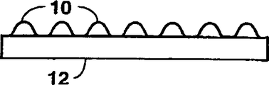
第1A図は従来のインク印刷法によって形成されたブラックマトリックスパターンの断面図、
第1B図は本発明の方法で転写層上に形成されたブラックマトリックスパターンの斜視図、
第2図は本発明にしたがって隆起ブラックマトリックスパターンを形成する装置を示す図、
第3図は隆起ブラックマトリックスパターンを形成する装置の他の例を示す図、
第4図は本発明にしたがって形成されたカラーフィルターパターンをガラス基板に移動させる工程を示す図、
第5図は本発明の方法を実施するための望ましい印刷装置を示す図である。
発明を実施するための最良の形態
本発明では転写層がコレクターロール等のコレクター装置上に形成される。次にその転写層上に所望のブラックマトリックスパターンに対応する隆起パターンがエンボスによって形成される。その隆起パターンに囲まれた凹部にレッド、グリーン、ブルーのカラードットパターンが形成され、得られる、転写層、隆起パターン(ブラックマトリックスパターンであってもそうでなくてもよい)およびカラーセルからなる複合材料が一工程でガラス基板に移動される。
転写層はブラックマトリックスパターンとレッド、グリーン、ブルー(またはイエロー、マゼンタ、シアン)各色のカラードットパターンを形成するための特殊な面を提供する。転写層にカラーフィルターパターンを形成することによって、その転写層、ブラックマトリックスパターン、およびカラードットパターンからなるアセンブリ全体をカラーフィルターが基板と転写層の間に挟まれるようにしてその基板上に移動させることができる。この転写層はそれ自体が平面化層として作用するから、平面化層を形成するための工程が不要になる。このような転写層については米国特許出願No.08/197,141に詳細に開示されている。この米国特許出願全文をここに引用したものとする。転写層の望ましい材料としては、ポリイミド、エポキシド、アクリレート、メタクリレート、ビニルエーテル、不飽和ポリエステルからなる群から選ばれるものがある。
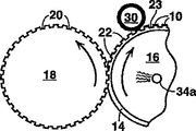
第2図はコレクターロールに転写層14を形成し、その転写層14に隆起パターンを形成するようにした本発明の方法を説明するためのものである。隆起パターンは様々な方法で転写層14上に形成することができる。例えば、第2図に示すように、転写層14が変形可能な状態にあるときに、転写層14を凹版ロール18(インクを乗せていない)に接触させる。その凹版ロール18には所望のブラックマトリックスパターンに対応する凹部パターン20が形成されている。そのため、変形可能な状態にある転写層14に所望のブラックマトリックスパターン10に対応する隆起パターン22が形成される。転写層14はこのようにして形成された隆起パターン22を保持できるように充分硬化させる必要がある。これは熱可塑性インクを使用し、ロール18との接点において転写層14を冷却してインクを硬化させることによって実行できる。より望ましい方法として、放射線硬化インクを使用し、隆起パターン22の形成中に紫外線ランプ34aからの放射線で転写層14を硬化させる方法がある。次にブラックマトリックスインクを隆起パターン22に塗布し、隆起ブラックマトリックスパターン10を形成する。第2図に示す実施の形態ではブラックマトリックスインク28をアプリケーターロール30で隆起パターン22に塗布して隆起ブラックマトリックスパターン10を形成する。ブラックマトリックス28は、液晶ディスプレイパネルの製造工程中に、他の部分に塗布してもよい。例えば、もう一方のガラス基板(薄膜トランジスタ用の)に塗布してもよい。さらには、薄膜トランジスタの頂面にブラックマトリックスパターンを形成してもよい。ブラックマトリックスパターンを薄膜トランジスタ基板上に形成する場合に、転写層14上での隆起パターン22の形成がレッド、グリーン、ブルーのカラーセルを互いに離隔してブラックマトリックスパターンと整列させるためのキーになるように思われる。次に隆起パターン22と整列するようにブラックマトリックスパターン10を位置決めすると、得られる液晶ディスプレイを見たときにブラックマトリックスパターン内にカラーセルが見える。
カラーフィルターパターンの残りの部分を構成するレッド、グリーン、ブルーのカラーインクセルを次に転写層14の隆起パターン22によって囲まれた凹部23内に形成する。次に、転写層14、ブラックマトリックスパターン10およびレッド、グリーン、ブルーのカラーセルからなる複合材料全体をガラス基板上に一度の工程で移動させる。
第3図は望ましい実施の形態を示すもので、凹版ロール18の凹部パターン20内にブラックマトリックスインクを付着させ、その凹部パターン20内で硬化させて、そのインクが凹部パターン20の形状を保持するようにする。次にそのインクを転写層14に転写する。望ましい実施の形態では、ブラックマトリックスインクとして放射線硬化型インクを使用し、転写層14への転写の前あるいは転写と同時に放射線によってインクを硬化させる。コレクターロール16上に透明な転写層14が形成される。後述するようにこの転写層14はインクアプリケターロールで形成してもよい。転写層14はブラックマトリックスパターンを受け取る前に半硬化させてもよいが、ブラックマトリックスパターンと接触させるまでは液体状態に保ち、ブラックマトリックスパターンの転写層14への転写の際に硬化させるのが望ましい。これは紫外線硬化型材料で転写層14を形成し、ブラックマトリックスパターン10を転写層14に転写する際に紫外線ランプ34aから紫外線を転写層14に放射することによって実行できる。コレクターロール16は紫外線を透過させる材料で形成されており、そのロール16内に紫外線ランプ34aが取り付けられる。転写層に使用されている光重合開始剤の種類によっては、可視光線、赤外線等の紫外線以外の放射線を使用することができる。第3図に示す方法によれば、従来可能と考えられていたものよりはるかに均一で正確なブラックマトリックスパターンが得られる。第1A図は、従来のインク印刷法によってガラス基板12上に形成した一般的なブラックマトリックスパターン10を構成するグリッドの断面図である。このような従来法によると、第1A図に示すようにインクの表面張力によって断面形状が円もしくは三角形に変形する傾向がある。またこの断面が円または三角形の線は時間がたつにつれて悪化し、細い線が滴になって切れてしまい鮮明度が失われてしまうこともある。また転写面(オフセット面)ないしガラス基板上でインクが乾いてしまって線が不連続になることもある。さらに、ブラックマトリックスのグリッドの交差部やパターンの面積に変化がある部分で、表面張力によってインクの移動が生ずることもある。さらに、このようなブラックマトリックスでは厚みが均一にならずしたがって光学濃度が均一にならない傾向がある。
第1B図は、第3図に示す方法によって転写層14上に形成したブラックマトリックスパターン10を示すものである。本発明の方法によれば、ブラックマトリックスインクは正確に凹部パターン20の形状を複写し、その形状を保持する。したがって、第3図に示すようにこのブラックマトリックスパターンのグリッドは全て直角なエッジを有する。したがって、完成した本発明によるブラックマトリックスパターンを見ると(矢印A方向に)、鮮明度の高い、直角に交差する(設計がそうなっている場合)厚みの均一な(光学濃度の均一な)グリッドのみが見える。以下に詳述するように、ブラックマトリックスパターン10によって形成された凹部11内にカラーインクセルが付着せしめられる。
第3図に示す装置は第2図に示す装置に似ているが、第3図の装置では凹版ロール18がブラックマトリックスインクパターン形成ロールとして使用される。第3図の凹版ロール18はインクを受け取る凹部パターン20を備えており、放射線硬化型、熱ワックス型あるいは溶液型のブラックマトリックスインクが凹部パターン20に供給される。望ましい実施の形態では、インクアプリケーターロール30が放射線硬化型ブラックマトリックスインク28を凹部パターン20に供給する。余分なインクはドクターブレード32でパターンから除去される。インクは凹部パターン20内で紫外線ランプ34からの紫外線を照射する等して硬化され、凹部パターン20の形状を少なくともほぼ保持するブラックマトリックスパターン10が形成される。あるいは、凹版ロール18を放射線透過材料で形成し、紫外線ランプ34cを凹版ロール18内に取り付け、インクが凹部パターン20内に保持されている間にそのインクを硬化または半硬化させるようにしてもよい。ブラックマトリックスインクの硬化はブラックマトリックスインクを転写層に接触させるのと同時に行ってもよい。例えば、紫外線ランプ34aからの放射線によってブラックマトリックスインクを硬化させてもよい。ブラックマトリックスインクの硬化が行われると、ブラックマトリックスは充分硬化して、インクは凹部パターン20の正確な形状を少なくともほぼ(望ましくは完全に)保持する。次ぎに、ブラックマトリックスパターン形成ロール18をコレクターロール16上の転写層14に接触させて、硬化したブラックマトリックスパターン10をロール18の凹部パターン20から転写層14に転写する。これによって第1B図に示すようなブラックマトリックスパターンが転写層14上に形成される。転写層14は滑らかであるのが望ましく、またブラックマトリックスパターンを受け取る前は液体状態であるのが望ましい。凹版像面がコレクターの表面より剥離性が高いことが重要である。凹版やグラビア印刷プレート内のインクは一般に負のメニスカスを有する。すなわち凹版の陰刻パターン内のインクの表面はプレート面の下方に湾曲する。したがって、転写層はブラックマトリックスインクに接触して付着し、凹版印刷パターンの凹部内のインクを取り出すことができるように充分軟らかく、粘着性でなければならない。凹版ロール18内でブラックマトリックスパターンが硬化せしめられる第3図に示す実施の形態では、ブラックマトリックスパターンの鮮明度は凹部パターン20の深さと形状およびこの形状が如何にうまくブラックマトリックスパターン10に与えられるかに依存している。ブラックマトリックスパターン10が凹部パターン20内にあるうちにブラックマトリックスパターン10を硬化させることによって、そのブラックマトリックスパターンは凹部パターンの直角なエッジと角を有する形状をとるようになる。このように本発明の方法によれば従来のインク印刷方法では一般的であった不規則で三角形ないし丸い角やエッジになることが避けられる。
第3図に示す方法は第2図に示す転写層成形工程の替わりにも使用できるし、その工程に加えて使用することもできる。すなわちもしその方が望ましければ、第1のロール18を使用して転写層14上に隆起パターンを形成し、その後第2のロール18を使用して、その隆起パターン22の上に硬化した隆起ブラックマトリックスパターンを付着させてもよい。
カラーフィルターを完成させるためにはカラーピクセルの形成が必要である。各カラーピクセルは一般にレッド、グリーン、ブルーのサブピクセルからなっている。(サブピクセルは本明細書ではカラーセルと称することもある)本発明の全ての実施の形態において、隆起パターン10(あるいは隆起ブラックマトリックスパターン10)を転写層14に形成した後、カラーフィルターパターンのレッド、グリーン、ブルーのカラーセルを転写層14上の隆起パターン10によって形成された凹部11内に付着させる。そのレッド、グリーン、ブルーのカラーセルは活版印刷技術によってブラックマトリックスパターン10内に付着させるのが望ましい。レッド、グリーン、ブルーのカラーインクセルを隆起パターン10内に付着させた後、転写層14、隆起パターン10およびレッド、グリーン、ブルーのカラーセル36からなる複合材料全体をガラス基板12に移動させる。
第4図は、ブラックマトリックスパターン10、カラーフィルターパターン36および転写層14のガラス基板12への移動を示している。第4図に示す複合材料は第3図に示す方法で形成したブラックマトリックスパターン10とカラーフィルターパターン36を含んでいる。複合材料を基板に移動する間は、レッド、グリーン、ブルーのカラーセルからなるインクセル36は液体あるいはその他の変形可能な状態であるのが望ましい。移動の間に、インクセルは転写層14とガラス基板12の間で圧縮され、より滑らかで、厚みがより均一なインクドットに変形する。この均一な形状と厚みは移動操作と同時にインクを硬化させることによって保持するのが望ましい。このようなインクの硬化はガラス基板を通して放射線を照射する紫外線ランプ34dによって実行することができる。移動操作の間に、インクセルが変形して、ブラックマトリックスパターンのグリッドによって形成された空間を完全に満たすのが望ましい。そのように変形する際にブラックマトリックスパターン10からインクセルがわずかに溢れることもあるが、そのような溢れは通常許容できる。
第5図は第3図に基づいて説明した方法を実施するための望ましい装置を示すものである。第5図の装置は、多色インクパターンを受け取る前に、コレクターロール16に比較的均一な厚みの透明な転写層14を塗布する転写層アプリケーターロール42を備えている。
転写層14の形成の後、隆起ブラックマトリックスパターンがブラックマトリックス像ロール18によって転写層14に形成される。ブラックマトリックス像ロール18は所望のブラックマトリックスパターンに対応する凹部パターン20を備えている。凹部パターン20にはブラックマトリックスインクロール30からブラックマトリックスインクが供給される。余分なインクはドクターブレード32によって凹部パターン20から除去され、凹部パターン20内のインクの厚みが均一にされる。そのブラックマトリックスインクはブラックマトリックス像ロール18の凹部パターン20内にある間に少なくとも半硬化される。これは転写層14へのブラックマトリックスパターン10の転写の前または転写と同時にブラックマトリックスパターン10を硬化させることによって実行できる。例えばある実施の形態では、ブラックマトリックス像ロール18が放射線透過型の材料で形成され、紫外線光源34cがそのロール18内に配され、その紫外線光源34cからの紫外線によってブラックマトリックスパターンが硬化される。あるいは、第5図に示すように、紫外線光源49をブラックマトリックスパターンロール18の上から紫外線を照射するように配してもよい。余分のブラックマトリックスインクをドクターブレード32で除去した後、紫外線光源49がインクに紫外線を照射し、ブラックマトリックスパターン形成ロール18の凹部パターン内にインクがある内にブラックマトリックスインクパターンを硬化させる。熱ワックス組成物の場合には冷却によって硬化させてもよいし、溶液型インクの場合には乾燥させて硬化させてもよいし、あるいはこのような硬化方法の組み合わせで硬化させてもよい。
硬化されたブラックマトリックスパターン10はブラックマトリックス像ロール18から転写層14に転写される。ブラックマトリックスパターンの転写の前は、凹部内のインクと密着するように転写層14が液体であるのが望ましい。半硬化されているときには、転写層はブラックマトリックスパターンに粘着して凹版ロール18からそのブラックマトリックスパターンを取り出すのに充分な粘着性を持っているのが望ましい。ブラックマトリックスパターン10と接触している間に、転写層14がその形状を維持できる程度またはロール18からブラックマトリックスパターン10を取り出せる程度に硬化されるのが望ましい。これはコレクターロール16を透明にし、そのロール16内に配された紫外線光源34aからの紫外線によって転写層14を硬化させることによって実行できる。転写層14上にブラックマトリックスパターンが形成された後、カラーフィルターパターンの残りの部分を構成するレッド、グリーン、ブルーのカラーセルパターンが転写層14上に付着される。以下に、レッド、グリーン、ブルーのカラーセルをコレクターロール16に支持された転写層14上のブラックマトリックスパターン10によって形成される凹部11内に付着させる方法について説明する。
第5図の装置において、多数の印刷パターンを有する1本の像パターンロール50を使用してレッド、グリーン、ブルーのカラードットパターンを形成する。
パターンロール50としては、リソグラフ、活版印刷、無水リソグラフ等、インクパターンないしインク像を形成できるものであれば事実上どのようなロールでも使用することができる。パターンロール50はフレキソグラフ等の活版印刷ロールであるのが望ましい。カラードットをロールではなく活版印刷プレートから転写してもよい。
第5図において、パターンロール50はブルー、グリーン、レッドのカラーインクパターンを形成するためのインクをそれぞれ受容する、3つのインク受容領域52a、52b、52cを有する活版印刷ロールである。3本のインク付けロール54が3つのインク受容領域52a、52b、52cにインク計量ロール56からそれぞれの色のインクを供給する。各インク付けロール54はパターンロール50と接触する位置に対して前後動できるようになっており、各色のインクが対応するインク受容領域にのみ供給されるようになっている。
コレクターロール16は2つの受容面58a、58bを備えており、各受容面58a、58bは、ブラックマトリックスと3色のピクセルカラーの全カラーフィルターパターンを転写層上に集める。パターンロール50のインク受容領域52a、52b、52c上に展開された各色のインクパターンはコレクターロール16の受容面58a、58bに位置合わせして印刷される。すなわち、インク受容領域52a、52b、52c上の各色のインクパターンは互いに特定の幾何学的関係を持ってコレクターロール16の受容面58a、58bに印刷される。この時、各色のインクはブラックマトリックスパターン内の対応する空間内に付けられる。
第5図においては、転写層アプリケーターロール42はコレクターロール16の受容面58bに転写層14を形成しており、ブラックマトリックスアプリケーターロール18は転写層14上に硬化したブラックマトリックスパターン10を転写している。この次には、レッドインクパターン領域52cがコレクターロール16の受容面58b上に赤のどっとパターンを付着させ、グリーンインクパターン領域52bがグリーンのドットパターンを受容面58aに付着させる。コレクターロール16の次の回転では、ブルーインクパターン領域52aがブルーのドットパターンを受容面58bに付着させ、レッドインクパターン領域52cが受容面58aに赤のドットパターンを付着させる。コレクターロール16のさらに次の回転では、グリーンインクパターン領域52bがグリーンのドットパターンを受容面58bに付着させ、ブルーインクパターン領域52aが受容面58aにブルーのドットパターンを付着させる。この時点で、各色のインクが、コレクターロール16の受容面58bに支持された転写層14上の隆起ブラックマトリックスパターン内に付着され、完全なカラーフィルターの像が現れる。このカラーフィルター像は、例えば、像解析検査装置あるいはレーザー走査型検査装置を用いた検査部60で検査される。もしその多色パターンが検査を通らなかった場合には、クリーニングロール64によって受容面58bから除去される。検査を通ったときには、真空チャック62に支持されているガラス基板12がコレクターロール16に接触せしめられ、転写層14、ブラックマトリックスパターン10およびレッド、グリーン、ブルーのカラーセルからなる複合材料がガラス基板12上に移される。
多色インクパターンの移動は多色像が変形可能な内に行うのが望ましい。これによって移動の際に、第4図に示すようにインクが転写層14とガラス基板12の間で圧縮される。望ましい実施の形態では、カラーインクセルには放射線硬化型のインクが使用され、真空チャック62は透明な材料で形成され、紫外線ランプ63がその真空チャック62内に配され、ガラス基板12を通して放射線を照射する。インクは移動操作中の圧力下で硬化され、移動操作によって与えられたより均一な形状を保持する。液晶ディスプレイカラーアレイの位置精度の要求は一般にプラスマイナス30ミクロン程度であり、将来はプラスマイナス5ミクロン程度になると考えられる。このような極めて厳しい位置精度の要求があるため、各色のパターンを1本のコレクターロール16上に1本のパターンロール50で形成するようにした第5図に示すような印刷機械は極めて有用である。まず第1に、パターンロール50とコレクターロール16の2本しかロールを使用しないため、整列させるべき機械部品が少ない。
コレクターロール16とパターンロール50が精度よく整列されたときに、パターンロール50上の各パターン52a、52b、52cが自動的にその位置を決めて各インクパターンをコレクターロール16に付着させるように、パターンロール50上での各パターン52a、52b、52c位置決めを正確に行えば位置合わせはより容易になる。複数のパターンロールを使用する従来技術の方法とは異なり、本発明の場合にはパターンロールは1本しか使用しない。全ての色のインクが転写層14に付けられると、形成された多色像全体が第4図に示すように一度の移動工程でコレクターロール16からガラス基板12に移される。
さらに、第5図の実施の形態では、パターンロール50からコレクターロール16への像転写比が3:2になっている。転写比はパターンロール50上の多色パターンの数とコレクターロール16上の受容面の数の比である。この3:2の転写比にすると、コレクターロール16の各回転毎に各インク領域がコレクターロール上の異なる受容面と接触するようになり、複数の像が一方のロールから他方のロールへ連続的に転写されることになる点で有利である。これは結果として自己割り出し操作になり(一旦操業運転にはいると)、全ての部品の間で正確な位置合わせが得られ、パターンロール50とコレクターロール16は一致した面速度モードの運転によってそれぞれの位置に維持される。
さらに、多色インクパターンは一工程で基板12に移される。したがって、多色インクパターンとブラックマトリックスを基板に移す際のコレクターロールと基板との位置合わせはたった一度でよい。これは、カラーフィルターパターンを三度に分けて基板に転写し、そのために基板との位置合わせを三度必要とした従来技術の方法と大きく異なるところである。
本発明の方法を実施する望ましい装置においては、第5図に示す装置は側面を下にして(すなわち印刷ロールを垂直に立てて)設置される。印刷ロールを垂直に取り付けると、ロールを垂直方向に(ロールの軸方向に)ロールを装置から取り外すことができる。これに対して、従来の装置ではロールは水平に配されており、水平方向に外さなければならなかった。
第5図の印刷ロールを端面を下にして支持することによって、従来技術の印刷装置に付き物であった多数の問題を解決することができる。まず、その方が良ければ、各印刷ロールを両端に配した2個の軸受けでなく、その下に配した1個の軸受けで支持することができる。これによって、反対側の端部(上端)がフリーになり、各印刷ロールを垂直方向に動かして取り外して交換することができる。したがって、印刷ロールの交換が大幅に容易になる。
インク(ブラックマトリックスインクやカラーインク)を硬化させるようにした実施の形態では、インクを放射線硬化させられるように調製するのが望ましい。「硬化させられる」とは「インクに架橋を起こさせることができる」という意味である。「放射線硬化させられる」とは「インクに所定の放射線を照射することによってインクに架橋を起こさせることができる」という意味である。これは硬化していない状態で(架橋を起こしていない状態で)そのインクがホットメルト熱可塑性を有しているか、あるいは溶剤を有するかとは関係ない。第5図に示す実施の形態では、真空チャック62は使用されるインクを硬化セルのに適した放射線を透過させる。例えば、真空チャック62は紫外線(160〜400μm)源あるいは可視光源(400〜700μm)を内部に備えており、そこから紫外線あるいは可視光を照射できるようになっている。インクに他の方法で放射線を照射してもよい。例えば、放射線源をロールと基板が複合材料挟む部分を照らすように位置させてもよい。このような放射線硬化は従来の放射線ランプを使用して行ってもよいが、レーザーをミラーで導いてインクを充分に硬化させてもよい。基板への移動の際にコレクターロール16によって変形された状態でドットを硬化させるためには、コレクターロールと基板との間の接触部分の表面積が、ドットが圧縮されている間に適当量の硬化ができるようにロールの回転速度に対して充分大きくなければならない。この接触領域は「足」と呼ばれるが、通常ガラスの上で5〜25mm幅である。
一般にカラーフィルターは約15〜25ミクロン幅のブラックマトリックス線と、幅約70〜100ミクロン、長さ160〜300ミクロンの小さなカラーセルとを必要とする。カラーセルは通常厚さ約10ミクロン未満、望ましくは5ミクロン未満の薄膜として印刷され、ブラックマトリックスパターン内に正しく位置され、均一に設けられなければならない。本発明を実施するのには、熱可塑性インクに比べて放射線硬化型インクの方が一般に望ましい。これは一つには、後者の方が前者に比べてより低い粘度で印刷でき、そのため上記のように極めて薄いセルを印刷しやすいからである。さらにホットメルト熱可塑性インクの場合には、パターンの寸法を制御するためには温度の許容度が極めて厳しく、パターンの位置合わせが困難である。さらに放射線硬化型インクの場合は、本発明の方法において圧縮移動操作の際にインクを硬化させるのが容易である。しかしながら熱可塑性インクも少なくとも一つは利点を持っている。それは、熱可塑性インクは低温の基板や転写ロールに付着すると直ぐに硬化するように配合できることである。これによってピンホール、膜厚の不均一等の転写面のぬれが不適当であるために生ずる欠陥を抑えることができる。したがって、熱可塑性と放射線硬化性の両方を備えているインクも望ましい。このようなインクは基板上に印刷されるまでは熱可塑性であるように配合され、印刷された時点で適切な放射線を照射して硬化させることのできるものである。ここで硬化とはインクがある程度架橋を起こすことである。インクが架橋を起こすと、耐久性と高温に対する耐性が増大する。これは以降の工程でカラーフィルターが曝される温度に鑑みて望ましいことである。
ブラックマトリックスインクとしては、揮発性の溶媒を加えて、インク付けおよびドクターの際の粘度を低下させるようにした溶媒型のインクも望ましい。溶媒としては、インクと調和し、転写層と接触する前に凹版プレート内において薄い(2〜5ミクロンが望ましい)ブラックマトリックスパターンから速やかに蒸発するものが選択される。その後、放射線あるいは熱によってインクに架橋を起こさせる。
基板への移動中あるいはその後に、放射線、熱、水分等に曝してインクを最終的に硬化させ、硬い、不粘着性の耐久性のある状態とする。
以上本発明を詳細に説明したが、これは単に説明のためであり、請求の範囲によって定義される本発明の精神と範囲に反することなく様々な変更を加えることができる。
例えば、上記実施の形態においては、転写層14をコレクターロール16に形成したが、プレート等の他のコレクター装置に形成しても差し支えない。同様に、上記実施の形態においては、パターンロールを使用したが平らなパターンプレートを使用してもよい。転写層14はどのような技法で形成してもよいが、インク塗布技法によって形成するのが望ましい。また第5図に示す方法の替わりに、前記3セットのカラーセルを個々のパターンロール54あるいは平らな像プレートからコレクターロール16に直接印刷してもよい。この場合にはパターンロール50を使用しない。
さらに上記実施の形態の殆どにおいては、ブラックマトリックスパターンがカラーフィルター基板上に形成されているが、第2図に関連して説明したように、ブラックマトリックスパターン10を液晶ディスプレイパネルの他の部分に形成してもよい。例えば、ブラックマトリックスパターンを薄膜トランジスタのガラス基板に形成してもよい。すなわち、第5図の実施の形態において、コレクターロール16をブラックマトリックスインクをブラックマトリックスインク凹版ロール18から直接受け取るのに使用してもよい。このインクは薄膜トランジスタガラス基板に直接転写される。この基板はブラックマトリックスパターンが薄膜トランジスタの上に形成されるように、薄膜トランジスタフィルムが張り合わせ済みのものを用いるのが望ましい。このブラックマトリックスインクは、望ましくは第2図を参照して説明したようにして、もう一つのガラス基板上に形成されたカラーフィルターパターンと整合される。 Technical field
The present invention relates to a color filter for a liquid crystal display panel, a black matrix pattern for the color filter, and a manufacturing method thereof.
Background art
Liquid crystal display (LCD) panels, particularly color LCD panels, are used in flat screen televisions, projection televisions, camcorder television finders, and the like, and are expected to be used in various fields in the future.
Manufacturing an active matrix liquid crystal display requires multiple steps. In the first step, a front glass panel is created. In this step, a color filter is provided on a suitable substrate such as glass. Usually, this color filter forms a black matrix pattern, and by forming a color dot pattern or color cell pattern of three primary colors (red, green, blue or yellow, magenta, cyan) within the area defined by the black matrix. It is formed. The printed lines forming the black matrix are generally about 15-25 microns wide and about 0.5-2 microns thick. Red, green and blue color cells are generally about 70-100 microns wide and about 200-300 microns long. The color cell is generally printed as a thin film having a thickness of less than about 10 microns, preferably less than 5 microns, and must be correctly positioned and uniformly provided in the pattern formed by the black matrix. The front glass substrate is usually further provided with a planarization layer, a transparent conductive layer and a polyimide alignment layer on the color filter. The transparent conductive layer is generally formed of indium tin oxide (ITO), but may be formed of other materials.
In the second step, another (rear) glass panel is used to form thin film transistors or thin film diodes and metal connection lines. Each transistor functions as an on / off switch for each color pixel in the liquid crystal display panel. In the last step, both panels are assembled and a liquid crystal material is injected between the panels to form a liquid crystal panel.
One of the most important steps in the production of color filters is the creation of a black matrix pattern. The edge sharpness or sharpness of the black matrix is particularly important. Unlike in the case of color ink cells, variations in the edge of the black matrix due to the flow of printing or the like can be easily found when inspecting the final product. On the other hand, the edge of the color pixel is usually hidden in the black matrix pattern. Therefore, the variation of the edge of the color pixel is hidden to some extent by the black matrix, but the variation of the edge of the black matrix cannot be hidden.
Since the black matrix pattern must be aligned with the transistors constituting the thin film transistors on the other glass panel, the requirement for positional accuracy is much stricter than that of the color dot pattern. On the other hand, the width of the black matrix pattern gives a slight margin to the positional accuracy of the color pixels. That is, the area between the individual color dots constituting the color pixel is hidden by the grid constituting the black matrix pattern. One typical black matrix pattern consists of a grid of elongated black lines that intersect with each other to form a rectangular region in which the ink of the color cell pixels is placed. Such a grid matrix further comprises a small black rectangle placed along the edge of the grid cell corresponding to the position of the thin film transistor (TFT) on the glass panel opposite the liquid crystal display. In the case of a black matrix pattern with a general rectangular sub-pixel grid pattern due to strict positional accuracy requirements, the black matrix is sharp when looking down from the color filter and only sharp edges are visible It is desirable to do. The cross-sectional shape of the grid constituting such a black matrix pattern also needs to be a rectangle having a right-angled edge. Also, the corners and intersections of such black matrix patterns are also right angles, and only the right edges need to be visible when looking down from the color filter. To date, there have been several printing techniques that can be used to produce the color ink dots that make up a color pixel, but the traditional requirement for thinner, and therefore higher resolution, black matrix lines is Printing technology can no longer respond. As this resolution limit is approached, it becomes extremely difficult to maintain the necessary sharpness using printing techniques. The biggest problem in printing technology is that the ink's surface tension tends to round the cross section of the ink, which makes the edges irregular.
Therefore, even if the other part of the color filter pattern is produced by a printing technique, the black matrix pattern is usually produced by a photolithographic method. This photolithographic process requires many steps, is much more complex than printing techniques, and is much more expensive.
Another important step in the manufacture of color filters is the formation of red, green and blue color dots (sometimes referred to as color cells). The color cell needs to be formed to be as smooth and uniform as possible. The method conventionally used for printing the color filter pattern is insufficient in the smoothness of the color pattern. This is mainly because the cross section of the ink cell is round or triangular in the conventional method of depositing ink. For this reason, it is common to form a planarization layer on the color pattern to correct defects related to smoothness and thickness uniformity caused by the adhesion method. The transparent planarization layer also helps to prevent ion migration to and from the ITO and color pattern layers. The planarization layer should be formed as smoothly and flat as possible.
In order to facilitate the formation of a flat planarization layer, it is desirable that the color pattern be smooth, flat and substantially flat on the lower surface of the glass substrate. If the thickness of the color pattern is not uniform, the intensity of transmitted light will fluctuate. Therefore, it is desirable that the thickness of the color pattern be uniform in order to improve the contrast and color performance of the display.
SUMMARY OF THE INVENTION An object of the present invention is to provide a black matrix pattern and an ink color filter array having high resolution, excellent positional accuracy, high quality and uniform thickness, and easier and at a lower cost than conventional color filter arrays. Is. Another object of the present invention is to provide the black matrix pattern and the ink color filter array as described above by a method having a smaller number of steps than the conventional method.
Disclosure of the invention
According to the present invention, a method for producing a color filter for a liquid crystal display is provided. In the present invention, a transfer layer is provided on a collector device such as a collector roll or a collector panel. A raised pattern is formed on the transfer layer. This raised pattern preferably corresponds to the desired black matrix pattern. A color filter pattern is formed by adhering red, green and blue color cells in the recesses formed by the raised pattern on the transfer layer. After the color pattern is formed on the transfer layer, the entire composite material of the transfer layer and the color filter pattern is transferred onto the glass substrate so that the color filter pattern is in contact with the glass substrate. In this state, the transfer layer is on the top and acts as a planarizing layer and a protective layer. The raised pattern on the transfer layer helps to maintain the separation between color cells during and after the printing operation.
The raised pattern on the transfer layer is preferably formed as a raised black matrix pattern. This raised black matrix pattern is not only useful for maintaining the separation between the color ink cells, but also helps to form a high definition black matrix pattern. The raised black matrix pattern means that when the transfer layer is on the surface of the collector, the upper surface of the black matrix pattern is higher than the upper surface of the transfer layer. The black matrix pattern preferably has a thickness (height from the rest of the transfer layer) of about 1 to 10 microns, more preferably about 2 to 6 microns, and 3 to 4 microns. Most desirable.
In one embodiment of the invention, prior to receiving the color cells that make up each pixel of the color filter, the transfer layer is contacted with a roll having a recessed pattern corresponding to the desired black matrix pattern. As a result, a raised pattern corresponding to a desired black matrix pattern is formed on the transfer layer. If necessary, a black matrix ink may be applied to the top surface of the raised pattern to form a raised black matrix pattern.
You may provide a black matrix pattern in the other part of a liquid crystal display panel. For example, it may be provided above or below a thin film transistor on a glass substrate carrying the thin film transistor. In this case, the black matrix pattern is desirably provided on the ITO layer. In such an embodiment, the raised pattern separates the red, green and blue color cells and serves primarily to align the color cells with the black matrix pattern. In order to form a raised black matrix pattern, it is desirable to form a black matrix ink pattern in the recesses of the intaglio image surface provided by an image roll, image plate or the like having an intaglio pattern corresponding to the desired black matrix pattern. It is desirable that the black matrix ink be cured, at least semi-cured before or during deposition on the transfer layer, so that the intaglio intaglio pattern is accurately copied. Inks in intaglios and gravure printing plates generally have a negative meniscus. That is, the surface of the ink in the intaglio intaglio pattern is curved below the plate surface. Therefore, it is desirable that the transfer layer be a liquid so that it can adhere to the ink when in contact with the black matrix ink. This liquid transfer layer is cured while in contact with the black matrix ink and removes the ink from within the intaglio pattern.
Ink printing is used to deposit red, green, and blue color cells in the recesses formed by the raised pattern (preferably a raised black matrix pattern). While the ink constituting the color cell can be deformed, the composite material composed of the transfer layer and the color ink cell (which may include a black matrix pattern) is transferred to the glass substrate. In this way, soft, deformable color ink cells are compressed between the transfer layer and the glass substrate. Since the color cell ink can be plastically deformed when transferred to the glass substrate, the red, green, and blue ink cells are compressed when transferred to the glass substrate, and the ink cells with originally non-uniform cross-sectional shape are flattened. This results in a color ink cell having a smoother, more even thickness and a smoother, more flat top surface than is possible with the prior art. Thus, the transfer layer serves to deform the color ink. After the transfer to the glass substrate, the transfer layer covers a multicolor ink pattern, so that the transfer layer also functions as a planarizing layer and a protective layer, and helps to maintain a more uniform ink cell shape. In this regard, it is the opposite of the conventional method of first attaching a color filter array to a substrate and forming a planarization layer in the next step. It is desirable to cure the ink sufficiently during or immediately after transfer to the glass substrate so that the shape of the crushed ink dots can be retained permanently. This can be done, for example, by curing the ink at the same time it is transferred to the glass substrate using radiation curable ink.
The transfer layer can be, for example, polyimide, epoxide, acrylic resin, vinyl ether, polyurethane, polyester, acrylated or methacrylated acrylic resin, ester, urethane, epoxide, or other materials used as planarizing layers in conventional color filters. Can be formed. Radiation curable acrylate materials such as radiation curable epoxy acrylate are desirable. The transfer layer is preferably formed of a radiation curable material so as to be cured while receiving the ink pattern constituting the black matrix pattern. The transfer layer is generally formed on the collector device as a thin film of less than 10 microns.
The method of the present invention is superior in many respects to the conventional black matrix pattern forming method. First, it is possible to form a very precise black matrix pattern with extremely sharp and right-angled edges. Therefore, the black matrix pattern according to the present invention is much sharper than that formed by the conventional method.
In addition, the transfer layer is formed on site.surfaceSince it functions as asurfaceSubsequent steps for forming the conversion layer are not necessary.
In addition, the ink used to form the red, green, and blue color cells can be deformed during movement to the glass substrate, thereby allowing color to be applied by the compressive force applied through the transfer layer from the collector roll. The ink cells can be deformed to have a more uniform shape. It is desirable to cure the ink under compression during the transfer operation to the glass substrate to maintain this more uniform dot shape. The transfer layer helps to protect and maintain this more uniform dot shape.
[Brief description of the drawings]
FIG. 1A is a cross-sectional view of a black matrix pattern formed by a conventional ink printing method,
FIG. 1B is a perspective view of a black matrix pattern formed on the transfer layer by the method of the present invention,
FIG. 2 shows an apparatus for forming a raised black matrix pattern according to the present invention;
FIG. 3 is a view showing another example of an apparatus for forming a raised black matrix pattern;
FIG. 4 is a diagram showing a process of moving a color filter pattern formed according to the present invention to a glass substrate;
FIG. 5 is a view showing a desirable printing apparatus for carrying out the method of the present invention.
BEST MODE FOR CARRYING OUT THE INVENTION
In the present invention, the transfer layer is formed on a collector device such as a collector roll. Next, a raised pattern corresponding to a desired black matrix pattern is formed on the transfer layer by embossing. A red, green, and blue color dot pattern is formed in a concave portion surrounded by the raised pattern, and the resulting pattern is composed of a transfer layer, a raised pattern (which may or may not be a black matrix pattern), and a color cell. The composite material is transferred to the glass substrate in one step.
The transfer layer provides a special surface for forming a black matrix pattern and color dot patterns of red, green, blue (or yellow, magenta, cyan) colors. By forming a color filter pattern on the transfer layer, the entire assembly comprising the transfer layer, black matrix pattern, and color dot pattern is moved onto the substrate so that the color filter is sandwiched between the substrate and the transfer layer. be able to. Since this transfer layer itself acts as a planarizing layer, a step for forming the planarizing layer is not necessary. Such a transfer layer is described in US Pat. 08/197, 141 in detail. The full text of this US patent application is hereby incorporated by reference. Desirable materials for the transfer layer include those selected from the group consisting of polyimide, epoxide, acrylate, methacrylate, vinyl ether, and unsaturated polyester.
FIG. 2 is a view for explaining the method of the present invention in which a
The red, green, and blue color ink cells that make up the remaining portion of the color filter pattern are then formed in a
FIG. 3 shows a preferred embodiment. A black matrix ink is deposited in the
FIG. 1B shows the
The apparatus shown in FIG. 3 is similar to the apparatus shown in FIG. 2, but the
The method shown in FIG. 3 can be used in place of the transfer layer forming step shown in FIG. 2, or can be used in addition to that step. That is, if that is desired, the
In order to complete the color filter, it is necessary to form color pixels. Each color pixel is generally composed of red, green, and blue sub-pixels. (Subpixels may also be referred to herein as color cells.) In all embodiments of the invention, after the raised pattern 10 (or raised black matrix pattern 10) is formed on the
FIG. 4 shows the movement of the
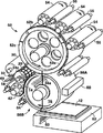
FIG. 5 shows a preferred apparatus for carrying out the method described with reference to FIG. The apparatus of FIG. 5 includes a transfer
After formation of the
The cured
In the apparatus shown in FIG. 5, red, green and blue color dot patterns are formed using one
As the
In FIG. 5, a
The
In FIG. 5, the transfer
It is desirable to move the multicolor ink pattern while the multicolor image is deformable. As a result, the ink is compressed between the
When the
Furthermore, in the embodiment of FIG. 5, the image transfer ratio from the pattern roll 50 to the
Furthermore, the multicolor ink pattern is transferred to the
In the preferred apparatus for practicing the method of the present invention, the apparatus shown in FIG. 5 is installed with the side down (i.e., with the print roll upright). When the printing roll is mounted vertically, the roll can be removed from the apparatus in the vertical direction (in the axial direction of the roll). On the other hand, in the conventional apparatus, the roll is arranged horizontally and has to be removed in the horizontal direction.
By supporting the printing roll of FIG. 5 with the end face down, a number of problems associated with the prior art printing apparatus can be solved. First, if it is better, each printing roll can be supported not by two bearings arranged at both ends but by one bearing arranged below it. As a result, the opposite end (upper end) becomes free, and each printing roll can be moved in the vertical direction to be removed and replaced. Therefore, the replacement of the printing roll is greatly facilitated.
In the embodiment in which the ink (black matrix ink or color ink) is cured, it is desirable to prepare the ink to be radiation-cured. “Curing” means “can cause crosslinking in the ink”. “Radiation-cured” means “the ink can be crosslinked by irradiating the ink with predetermined radiation”. This is unrelated to whether the ink has hot melt thermoplasticity or has a solvent in an uncured state (in the absence of crosslinking). In the embodiment shown in FIG. 5, the
Color filters generally require black matrix lines about 15-25 microns wide and small color cells about 70-100 microns wide and 160-300 microns long. The color cell is usually printed as a thin film with a thickness of less than about 10 microns, preferably less than 5 microns, and must be correctly positioned and uniformly provided within the black matrix pattern. In order to carry out the present invention, a radiation curable ink is generally more desirable than a thermoplastic ink. This is partly because the latter can be printed with a lower viscosity than the former, so that it is easier to print very thin cells as described above. Furthermore, in the case of a hot melt thermoplastic ink, the temperature tolerance is extremely strict in order to control the dimension of the pattern, and it is difficult to align the pattern. Furthermore, in the case of radiation curable ink, it is easy to cure the ink during the compression movement operation in the method of the present invention. However, at least one thermoplastic ink has advantages. That is, the thermoplastic ink can be formulated so as to be cured as soon as it adheres to a low temperature substrate or transfer roll. As a result, defects caused by improper wetting of the transfer surface such as pinholes and uneven film thickness can be suppressed. Thus, inks that are both thermoplastic and radiation curable are also desirable. Such an ink is formulated so as to be thermoplastic until it is printed on a substrate, and can be cured by irradiation with appropriate radiation at the time of printing. Here, curing means that the ink is crosslinked to some extent. When the ink is crosslinked, durability and resistance to high temperatures increase. This is desirable in view of the temperature to which the color filter is exposed in subsequent steps.
As the black matrix ink, a solvent-type ink in which a volatile solvent is added to reduce the viscosity at the time of inking and doctoring is also desirable. Solvents are selected that are compatible with the ink and that quickly evaporate from a thin (preferably 2-5 microns) black matrix pattern in the intaglio plate before contacting the transfer layer. Thereafter, the ink is crosslinked by radiation or heat.
During or after the transfer to the substrate, the ink is finally cured by exposure to radiation, heat, moisture, etc., to obtain a hard, non-tacky and durable state.
Although the present invention has been described in detail above, this is merely for the purpose of illustration and various changes can be made without departing from the spirit and scope of the invention as defined by the claims.
For example, in the above embodiment, the
Further, in most of the above embodiments, the black matrix pattern is formed on the color filter substrate. However, as described with reference to FIG. 2, the
Claims (22)
その転写層に隆起パターンと凹部パターンとを形成し、
その転写層の前記凹部パターン内に複数のカラーインクパターンを形成して、カラーフィルターパターンと転写層から成る複合材料を形成し、
その複合材料を基板上に、前記インクパターンがその基板と接触するようにして移動し、前記転写層を現場で形成される平面化層として機能させる、
ことを特徴とするカラーフィルターの製造方法。Providing a transfer layer,
A raised pattern and a recessed pattern are formed on the transfer layer,
A plurality of color ink patterns are formed in the recess pattern of the transfer layer to form a composite material composed of a color filter pattern and a transfer layer,
The composite material on the substrate, wherein the ink pattern is moved so as to contact with the substrate, thereby the function as a flat surface layer formed of the transfer layer in situ,
A method for producing a color filter, comprising:
凹部パターンを設け、
その凹部パターン内にインクを付着させ、その凹部パターン内の前記インクを前記転写層に転写して、その転写層上に隆起ブラックマトリックスパターンを形成する、
各工程を含むことを特徴とする請求の範囲第1項記載の方法。The step of forming a raised pattern and a recessed pattern in the transfer layer,
Providing a concave pattern,
Ink is deposited in the recess pattern, the ink in the recess pattern is transferred to the transfer layer, and a raised black matrix pattern is formed on the transfer layer.
2. A method according to claim 1 comprising each step.
前記コレクターロールに前記転写層を形成する転写層アプリケーター、
ブラックマトリックスパターンに対応する凹部パターンを有し、前記コレクターロール上の前記転写層に接触せしめられるブラックマトリックスパターンロール、および
前記転写層にカラーインクを付着させて、前記転写層とカラーフィルターパターンから成る複合材料を形成する少なくと1本のカラーインクロール、
を有してなり、これらコレクターロール、転写層アプリケーター、ブラックマトリックスパターンロールおよびカラーインクロールが軸方向において垂直に設置されていることを特徴とするカラーフィルター印刷装置。A collector roll that receives a composite material comprising a transfer layer and a color filter pattern and moves the composite material to a substrate;
A transfer layer applicator for forming the transfer layer on the collector roll;
A black matrix pattern roll having a concave pattern corresponding to the black matrix pattern and contacting the transfer layer on the collector roll, and color ink is attached to the transfer layer, and the transfer layer and the color filter pattern are formed. At least one color ink roll forming a composite material;
A color filter printing apparatus comprising: a collector roll, a transfer layer applicator, a black matrix pattern roll, and a color ink roll arranged vertically in the axial direction .
Applications Claiming Priority (3)
| Application Number | Priority Date | Filing Date | Title |
|---|---|---|---|
| US08/324,345 | 1994-10-17 | ||
| US08/324,345 US5514503A (en) | 1994-10-17 | 1994-10-17 | Apparatus and method for printing a color filter |
| PCT/US1995/017146 WO1996036491A2 (en) | 1994-10-17 | 1995-10-04 | Apparatus and method for printing a color filter |
Publications (2)
| Publication Number | Publication Date |
|---|---|
| JPH11506985A JPH11506985A (en) | 1999-06-22 |
| JP3931925B2 true JP3931925B2 (en) | 2007-06-20 |
Family
ID=23263196
Family Applications (1)
| Application Number | Title | Priority Date | Filing Date |
|---|---|---|---|
| JP52285996A Expired - Fee Related JP3931925B2 (en) | 1994-10-17 | 1995-10-17 | Color filter printing apparatus and printing method |
Country Status (9)
| Country | Link |
|---|---|
| US (1) | US5514503A (en) |
| EP (1) | EP0768955A1 (en) |
| JP (1) | JP3931925B2 (en) |
| KR (1) | KR100382052B1 (en) |
| BR (1) | BR9508182A (en) |
| CA (1) | CA2183983A1 (en) |
| MX (1) | MX9602375A (en) |
| TW (1) | TW294841B (en) |
| WO (1) | WO1996036491A2 (en) |
Families Citing this family (44)
| Publication number | Priority date | Publication date | Assignee | Title |
|---|---|---|---|---|
| US5535673A (en) * | 1993-11-03 | 1996-07-16 | Corning Incorporated | Method of printing a color filter |
| US5624775A (en) * | 1994-02-16 | 1997-04-29 | Corning Incorporated | Apparatus and method for printing a color filter |
| US5752442A (en) * | 1993-11-03 | 1998-05-19 | Corning Incorporated | Method for printing a color filter |
| US5972545A (en) * | 1993-11-03 | 1999-10-26 | Corning Incorporated | Method of printing a color filter |
| EP0726851A4 (en) * | 1993-11-03 | 1997-04-16 | Corning Inc | Color filter and method of printing |
| US6001515A (en) * | 1993-11-03 | 1999-12-14 | Corning Incorporated | Method for printing a color filter |
| US5678483A (en) * | 1994-02-16 | 1997-10-21 | Corning Incorporated | Method for printing a black border for a color filter |
| US6120946A (en) * | 1994-10-17 | 2000-09-19 | Corning Incorporated | Method for printing a color filter |
| JP3059678B2 (en) * | 1995-07-14 | 2000-07-04 | キヤノン株式会社 | Method and apparatus for manufacturing color filter |
| GB9623185D0 (en) * | 1996-11-09 | 1997-01-08 | Epigem Limited | Improved micro relief element and preparation thereof |
| US6152033A (en) * | 1997-08-29 | 2000-11-28 | Corning Incorporated | Method of making an electronic printed structure |
| US6412305B1 (en) | 1998-12-21 | 2002-07-02 | Corning Incorporated | Method of manufacturing opaque rib structures for display panel |
| US6620370B2 (en) | 1998-12-21 | 2003-09-16 | Corning Incorporated | Method for manufacturing opaque rib structures for display panels |
| US6272275B1 (en) | 1999-06-25 | 2001-08-07 | Corning Incorporated | Print-molding for process for planar waveguides |
| KR100649722B1 (en) * | 2000-04-21 | 2006-11-24 | 엘지.필립스 엘시디 주식회사 | Apparatus for Patterning Electro-luminescence Display Device and Method of Patterning Electro-luminescence Display Device using the same |
| JP3757777B2 (en) * | 2000-09-29 | 2006-03-22 | セイコーエプソン株式会社 | Manufacturing method of electro-optical device |
| US6732643B2 (en) | 2001-11-07 | 2004-05-11 | Lg. Philips Lcd Co., Ltd. | Method for forming pattern using printing process |
| US7569153B2 (en) * | 2002-05-23 | 2009-08-04 | Lg Display Co., Ltd. | Fabrication method of liquid crystal display device |
| US20040247906A1 (en) * | 2002-05-24 | 2004-12-09 | Optical Coating Laboratory, Inc., A Jds Uniphase Company | Coating for forming a high definition aperture |
| JP4111116B2 (en) * | 2002-12-05 | 2008-07-02 | 株式会社村田製作所 | Method for forming thick film wiring and method for manufacturing multilayer electronic component |
| KR100909414B1 (en) | 2002-12-18 | 2009-07-24 | 엘지디스플레이 주식회사 | Manufacturing method of liquid crystal display element |
| KR100585871B1 (en) * | 2002-12-18 | 2006-06-02 | 엘지.필립스 엘시디 주식회사 | A method of forming pattern using printing process |
| KR100518270B1 (en) * | 2002-12-18 | 2005-10-04 | 엘지.필립스 엘시디 주식회사 | Method of forming pattern using printing process |
| KR100914200B1 (en) * | 2002-12-27 | 2009-08-27 | 엘지디스플레이 주식회사 | Fabricating method of liquid crystal display device |
| KR100909419B1 (en) * | 2002-12-27 | 2009-07-28 | 엘지디스플레이 주식회사 | Method for manufacturing color filter of liquid crystal display device |
| KR100945357B1 (en) * | 2002-12-27 | 2010-03-08 | 엘지디스플레이 주식회사 | Fabrication method of liquid crystal display |
| KR100905017B1 (en) * | 2002-12-27 | 2009-06-30 | 엘지디스플레이 주식회사 | Liquid crystal display device and fabrication method thereof |
| KR100606446B1 (en) * | 2002-12-27 | 2006-07-31 | 엘지.필립스 엘시디 주식회사 | Fabrication method of liquid crystal display device |
| KR100945356B1 (en) * | 2002-12-27 | 2010-03-09 | 엘지디스플레이 주식회사 | Fabrication method of color filter of liquid crystal display device |
| KR100945349B1 (en) * | 2002-12-28 | 2010-03-08 | 엘지디스플레이 주식회사 | Color filter fabrication method of liquid crystal display device |
| KR100909422B1 (en) | 2002-12-31 | 2009-07-24 | 엘지디스플레이 주식회사 | Pattern of Liquid Crystal Display and Formation Method |
| JP4715150B2 (en) * | 2004-09-30 | 2011-07-06 | 凸版印刷株式会社 | Pattern forming method and pattern forming apparatus |
| JP4710296B2 (en) * | 2004-09-30 | 2011-06-29 | 凸版印刷株式会社 | Pattern forming method and pattern forming apparatus |
| JP4765288B2 (en) * | 2004-09-30 | 2011-09-07 | 凸版印刷株式会社 | Pattern forming method and pattern forming apparatus |
| CN100529875C (en) * | 2005-03-19 | 2009-08-19 | 鸿富锦精密工业(深圳)有限公司 | Method of manufacturing color filter |
| JP4797414B2 (en) * | 2005-03-23 | 2011-10-19 | 凸版印刷株式会社 | Method for forming black matrix of color filter and method for forming color filter |
| KR100634327B1 (en) * | 2005-04-13 | 2006-10-13 | 한국기계연구원 | Electronic element production method and production device |
| KR100981021B1 (en) * | 2007-03-09 | 2010-09-07 | 주식회사 엘지화학 | Method and system for forming black matrix |
| JP5109446B2 (en) * | 2007-03-30 | 2012-12-26 | ソニー株式会社 | Pattern forming method and electronic device manufacturing method |
| KR101147111B1 (en) | 2009-08-26 | 2012-05-17 | 주식회사 파인텍 | Method of Fabricating Image Display Device |
| KR101147114B1 (en) | 2009-08-26 | 2012-05-17 | 주식회사 파인텍 | Method of Manufacturing Image Display Device |
| WO2011139882A2 (en) * | 2010-05-04 | 2011-11-10 | Unipixel Displays, Inc. | Method of fabricating micro structured surfaces with electrically conductive patterns |
| KR101362065B1 (en) * | 2012-07-25 | 2014-02-21 | 주식회사 엘지화학 | Flexible color filter substrate using a phase change ink and method for manufacturing thereof |
| CN104777664A (en) * | 2015-04-28 | 2015-07-15 | 深圳市华星光电技术有限公司 | Method for manufacturing black matrix |
Family Cites Families (7)
| Publication number | Priority date | Publication date | Assignee | Title |
|---|---|---|---|---|
| US4035214A (en) * | 1975-07-21 | 1977-07-12 | American Can Company | Total image transfer process |
| JPS61284441A (en) * | 1985-06-11 | 1986-12-15 | Takahane Sangyo Kk | Offset printing press and printing method |
| KR0153260B1 (en) * | 1989-06-16 | 1998-11-02 | 기다지마 요시도시 | Method of printing fine patterns |
| KR920005444B1 (en) * | 1989-12-02 | 1992-07-04 | 삼성전자 주식회사 | Method of manufacturing color filter |
| JPH0516324A (en) * | 1991-07-10 | 1993-01-26 | Fuji Photo Film Co Ltd | Printing device |
| JPH05147359A (en) * | 1991-11-27 | 1993-06-15 | Dainippon Printing Co Ltd | Forming method for fine pattern |
| EP0726851A4 (en) * | 1993-11-03 | 1997-04-16 | Corning Inc | Color filter and method of printing |
-
1994
- 1994-10-17 US US08/324,345 patent/US5514503A/en not_active Expired - Fee Related
-
1995
- 1995-10-04 MX MX9602375A patent/MX9602375A/en unknown
- 1995-10-04 BR BR9508182A patent/BR9508182A/en not_active Application Discontinuation
- 1995-10-04 WO PCT/US1995/017146 patent/WO1996036491A2/en not_active Application Discontinuation
- 1995-10-04 EP EP95944852A patent/EP0768955A1/en not_active Withdrawn
- 1995-10-04 CA CA002183983A patent/CA2183983A1/en not_active Abandoned
- 1995-10-17 JP JP52285996A patent/JP3931925B2/en not_active Expired - Fee Related
- 1995-11-30 TW TW084112865A patent/TW294841B/zh active
-
1996
- 1996-06-17 KR KR10-1997-0704225A patent/KR100382052B1/en not_active IP Right Cessation
Also Published As
| Publication number | Publication date |
|---|---|
| KR100382052B1 (en) | 2003-08-30 |
| CA2183983A1 (en) | 1996-11-21 |
| US5514503A (en) | 1996-05-07 |
| BR9508182A (en) | 1997-08-12 |
| WO1996036491A2 (en) | 1996-11-21 |
| TW294841B (en) | 1997-01-01 |
| MX9602375A (en) | 1997-02-28 |
| WO1996036491A3 (en) | 1997-03-20 |
| EP0768955A1 (en) | 1997-04-23 |
| JPH11506985A (en) | 1999-06-22 |
Similar Documents
| Publication | Publication Date | Title |
|---|---|---|
| JP3931925B2 (en) | Color filter printing apparatus and printing method | |
| JP4291411B2 (en) | Apparatus and method for printing color filters | |
| US6001515A (en) | Method for printing a color filter | |
| US5678483A (en) | Method for printing a black border for a color filter | |
| KR100326281B1 (en) | Color filter and its manufacturing method | |
| US5540147A (en) | Method for forming a contoured planarizing layer for a color filter | |
| JP3559044B2 (en) | Color filter and printing method | |
| US20070214977A1 (en) | Color filter printing method, color filter printing apparatus, and color filter substrate | |
| US5752442A (en) | Method for printing a color filter | |
| JPH08262220A (en) | Color fiter, its production and liquid crystal display device with same | |
| JP4364534B2 (en) | Image forming method | |
| JP2001249342A (en) | Method of positioning spacer bead and liquid crystal display device | |
| KR100638410B1 (en) | Method of Making an Imaged Ink Pattern | |
| JP2005115000A (en) | Method and device of printing minute pattern, and color filter | |
| CN1153496A (en) | Apparatus and method for printing color-filter | |
| JPH09171107A (en) | Color filter and preparation thereof | |
| KR20040050770A (en) | method of color filter panel for liquid crystal display | |
| JPH03221484A (en) | Printing method and printing device | |
| JPH05288917A (en) | Manufacture of color filter | |
| JPH0743514A (en) | Production of color filter | |
| JP4710296B2 (en) | Pattern forming method and pattern forming apparatus | |
| JPH07244211A (en) | Method for flattening pattern surface |
Legal Events
| Date | Code | Title | Description |
|---|---|---|---|
| A131 | Notification of reasons for refusal |
Free format text: JAPANESE INTERMEDIATE CODE: A131 Effective date: 20051108 |
|
| A524 | Written submission of copy of amendment under section 19 (pct) |
Free format text: JAPANESE INTERMEDIATE CODE: A524 Effective date: 20060207 |
|
| A131 | Notification of reasons for refusal |
Free format text: JAPANESE INTERMEDIATE CODE: A131 Effective date: 20060919 |
|
| A524 | Written submission of copy of amendment under section 19 (pct) |
Free format text: JAPANESE INTERMEDIATE CODE: A524 Effective date: 20061218 |
|
| TRDD | Decision of grant or rejection written | ||
| A01 | Written decision to grant a patent or to grant a registration (utility model) |
Free format text: JAPANESE INTERMEDIATE CODE: A01 Effective date: 20070220 |
|
| A61 | First payment of annual fees (during grant procedure) |
Free format text: JAPANESE INTERMEDIATE CODE: A61 Effective date: 20070306 |
|
| R150 | Certificate of patent or registration of utility model |
Free format text: JAPANESE INTERMEDIATE CODE: R150 |
|
| LAPS | Cancellation because of no payment of annual fees |