JP3927770B2 - Method and apparatus for selecting power supply voltage of line circuit - Google Patents
Method and apparatus for selecting power supply voltage of line circuit Download PDFInfo
- Publication number
- JP3927770B2 JP3927770B2 JP2000552839A JP2000552839A JP3927770B2 JP 3927770 B2 JP3927770 B2 JP 3927770B2 JP 2000552839 A JP2000552839 A JP 2000552839A JP 2000552839 A JP2000552839 A JP 2000552839A JP 3927770 B2 JP3927770 B2 JP 3927770B2
- Authority
- JP
- Japan
- Prior art keywords
- power supply
- supply voltage
- line
- line circuit
- voltage
- Prior art date
- Legal status (The legal status is an assumption and is not a legal conclusion. Google has not performed a legal analysis and makes no representation as to the accuracy of the status listed.)
- Expired - Fee Related
Links
Images

Classifications
-
- H—ELECTRICITY
- H04—ELECTRIC COMMUNICATION TECHNIQUE
- H04M—TELEPHONIC COMMUNICATION
- H04M19/00—Current supply arrangements for telephone systems
-
- H—ELECTRICITY
- H04—ELECTRIC COMMUNICATION TECHNIQUE
- H04M—TELEPHONIC COMMUNICATION
- H04M19/00—Current supply arrangements for telephone systems
- H04M19/001—Current supply source at the exchanger providing current to substations
-
- H—ELECTRICITY
- H04—ELECTRIC COMMUNICATION TECHNIQUE
- H04M—TELEPHONIC COMMUNICATION
- H04M19/00—Current supply arrangements for telephone systems
- H04M19/001—Current supply source at the exchanger providing current to substations
- H04M19/005—Feeding arrangements without the use of line transformers
Landscapes
- Engineering & Computer Science (AREA)
- Signal Processing (AREA)
- Power Engineering (AREA)
- Devices For Supply Of Signal Current (AREA)
- Power Sources (AREA)
- Control Of Electrical Variables (AREA)
- Measurement Of Current Or Voltage (AREA)
- Direct Current Feeding And Distribution (AREA)
Description
【0001】
(技術分野)
本発明は一般的にライン・インターフェイス・ボードに関するものであり,特にライン・インターフェイス・ボード上の線路回路の電力消費量を最小にすることに関するものである。
【0002】
(発明の背景)
2線式線路を駆動する加入者のライン・インターフェイス回路では,線路電流も線路電圧も線路負荷,すなわち電話機および線路自体の抵抗,の関数である。
【0003】
線路が開放されている場合,電流がゼロのとき線路には最大電圧が供給される。線路回路が動作するためには,線路回路を電源電圧に接続しなければならない。電源電圧は必要な線路電圧よりも幾分高い。
【0004】
線路が閉じている場合,すなわち線路に負荷がかかっている場合,線路抵抗と負荷抵抗の和にしたがって線路電圧は減少し,線路電流は増加するであろう。
【0005】
電源電圧と線路電圧の差は線路電流が流れる線路回路に加わる。このために,線路回路内で電力が消費される。
【0006】
線路回路内の電力消費量は線路を短絡したとき,すなわち線路と負荷の合計抵抗値が低いとき,最大になる。
【0007】
多くの場合,線路回路内の電力消費,すなわち電力損失は容認される。
【0008】
ある場合には,最大電力消費量を低く保つために,各線路ごとにDC/DCコンバータを使うことができる。それぞれのコンバータから供給される出力電圧は,瞬時の線路負荷に適応するために連続的に制御される。しかし,そのようなコンバータを使うと,放射を乱したり回路の複雑性を増す原因となる。
【0009】
WO 96/15617から,電力消費量を最小にするために駆動電圧の数に相当するいくつかのアナログ直列調整器を使うことが知られている。これは電源電圧をその瞬間に必要な最低の電源電圧の絶対値を有する電源電圧にスイッチングすることによって行うものである。
【0010】
たとえば2種類の電源電圧を用いて上記スイッチング方式を有する線路回路を使うとき,低い方の絶対値を有する電圧をあらかじめ定めた固定値に設定する。固定値には電力消費量が最低であることが期待される値を選ぶ。このあらかじめ定めた値を通常すべてのインターフェイスボードに設定する。高い方の絶対値を有する電圧は通常電池の電圧である。
【0011】
(発明の要約)
本発明の目的はライン・インターフェイス・ボード上の線路回路の電力消費量を更に少なくすることである。
【0012】
このことは実際の線路電圧に応じて電源電圧を適応させる本発明により達成される。
【0013】
そのことにより,ライン・インターフェイス・ボード上の線路回路の電力消費量を更に少なくすることが可能になるであろう。
【0014】
(発明の実施の形態)
次に本発明について,図面を参照して詳しく説明する。
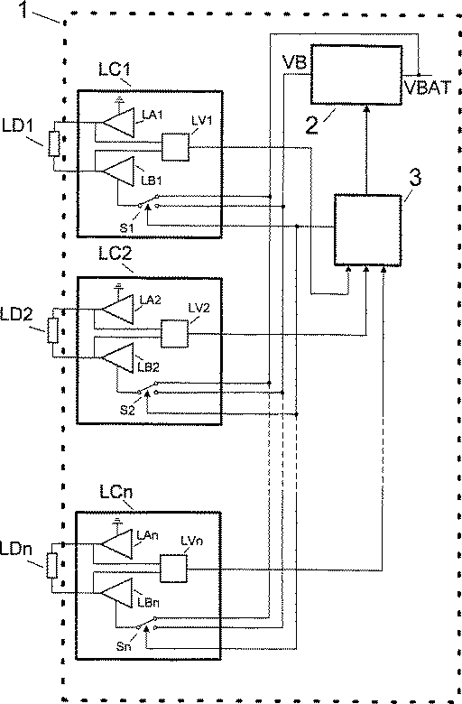
図はいくつかの線路回路LC1,LC2…LCnを有するライン・インターフェイス・ボード1を示す.ここでnはたとえば16である。
【0015】
これ自体はよく知られているように,2線式線路は線路回路LC1,LC2…LCnに接続されており,図示の如く,線路はそれぞれのインピーダンスLD1,LD2…LDnで終端していることとする。
【0016】
それぞれの線路回路において,線路のそれぞれの線は増幅器LA1,LA2…LAnとLB1,LB2…LBnによりそれぞれ駆動される。
【0017】
本発明によれば,これらの増幅器にはライン・インターフェイス・ボード1上の線路回路LC1,LC2…LCnの合計電力消費量ができるだけ低く保たれるように給電される。
【0018】
図示した実施例では,線路回路LC1,LC2…LCnには電池の固定電圧VBATか,またはVBATよりも低い絶対値を有する可変電圧VBのいずれかが供給されることとする。
【0019】
この接続において,VBATもまた可変でありうることを指摘しておく。
【0020】
図示した本発明の実施例では,電源電圧をVBATとVBとの間で切り替えるために,各線路回路LC1,LC2…LCn内にスイッチS1,S2…Snが設けられている。これらのスイッチはもちろん線路回路の外側においても全く問題ないであろう。
【0021】
制御可能なDC/DCコンバータ2がライン・インターフェイス・ボード1上に設けられていて,プロセッサ3から発せられる信号の制御下で,VBATからVBを発生する。
【0022】
プロセッサ3は後述するように,スイッチS1,S2…Snを制御するように作られている。
【0023】
本発明のこの実施例では,各線路回路LC1,LC2…LCnにそれぞれの線路回路LC1,LC2…LCnの線路電圧を測定するための回路LV1,LV2…LVnが設けられている。それぞれの回路LV1,LV2…LVnにより測られた線路電圧はプロセッサ3の入力信号として供給される.線路電圧を測定するための回路は線路回路の外側においても全く問題ないであろうことは理解されよう。
【0024】
測定された線路電圧に基づいて,プロセッサ3は電源電圧VBの候補値をいくつか予測するように作動する。また,プロセッサ3は回路LV1,LV2…LVnから得られた線路電圧の測定値に基づいて,それぞれの線路回路LC1,LC2…LCnに電源電圧VBとして予測したそれぞれの候補値を供給することができるか否かを決定する。
【0025】
電源電圧VBとして予測したそれぞれの候補値を供給することができる線路回路について,プロセッサ3はVBの各候補値毎にこれらの線路回路の電力消費量を計算するように作動する。
【0026】
電源電圧VBとして予測した候補値を供給することができない線路回路の場合,プロセッサ3は固定の電池電圧VBTを用いてこれらの線路回路の電力消費量を計算するように作動する。
【0027】
電源電圧VBの各候補値毎に,プロセッサ3はライン・インターフェイス・ボード1上の各線路回路の電力消費量を加算するように作動する。
【0028】
好ましくは,作動している回路の電力消費量だけを計算して加算する。
【0029】
使用すべき電源電圧VBの値を選択するには,プロセッサ3はライン・インターフェイス・ボード1上の作動している線路回路の電力消費量の合計が最低になるような値を選択する。
【0030】
電池電圧VBATか,またはプロセッサ3から供給される入力信号に応じてコンバータ2により作られた電源電圧VBの選択された値のいずれかを選んで,電源電圧としてライン・インターフェイス・ボード1上の線路回路に供給する。そのために,プロセッサ3はスイッチS1,S2…Snの位置を制御して,それぞれの線路回路にVBATかVBの選択された値かのいずれかが接続するように作動する。
【0031】
以下実用的な例を述べる。
【0032】
ライン・インターフェイス・ボード1上に3個の作動中の線路回路があって,それらの線路電圧がそれぞれ13V,40V,23Vであるとする.線路電流は一定で,0,027Aとする。|VBAT|=48Vとする。
【0033】
線路回路にVBを供給するために,VB>=線路電圧の測定値+6Vとする。
【0034】
VB を 28V に固定する
【0035】
ライン・インターフェイス・ボードを実装する前に,すべてのライン・インターフェイス・ボードの線路電圧を調べる。最適なVBの値が28Vであるとわかったとする。その結果,すべてのライン・インターフェイス・ボードでVBを28Vに設定する。
【0036】
作動している線路回路のうち1個にVB=28V を供給すると,残りの2個の線路回路にはVBAT=48Vを供給しなければならない。
【0037】
すると,3個の作動中の線路回路における電力消費量は以下のようになるであろう。
【0038】
【数1】
VB を適応性にする
【0040】
線路電圧の測定値,すなわちそれぞれ13V,40V,23V,に6Vを加えることによってVBの3個の候補値を予測する。
【0041】
したがって,VBとして以下の3個の候補値が予測される。
【0042】
【数2】
【数3】
【数4】
VB1=19Vの場合,1個の線路回路だけにこの線路電圧を供給することができて,残りの2個の線路回路にはVBAT=48Vを供給しなければならない。
【0046】
したがって,ライン・インターフェイス・ボード上の電力消費量は以下のようになるであろう。
【0047】
【数5】
VB2=29Vの場合,2個の線路回路にこの線路電圧を供給することができて,第3の線路回路にはVBAT=48Vを供給しなければならない。
【0049】
したがって,ライン・インターフェイス・ボード上の電力消費量は以下のようになるであろう。
【0050】
【数6】
VB3=46Vの場合,3個の線路回路すべてにこの線路電圧を供給することができる。
【0052】
この場合,ライン・インターフェイス・ボード上の電力消費量は以下のようになるであろう。
【0053】
【数7】
上記の説明から明らかなように,VB1=19V,VB2=29Vどちらの場合もVBを常に28Vに固定したときよりも電力消費量は少ないという結果になる。
【0055】
この例ではVB2=29Vのとき消費電力量が最低であるから,プロセッサ3はコンバータ2で作られる電圧VBとしてこの値を選択するように作動する。
【0056】
それから,プロセッサ3はスイッチS1,S2…Snの位置を制御して,それぞれの線路回路LC1,LC2…LCnにVBATかVBのいずれかを供給する。
【図面の簡単な説明】
【図1】 本発明による装置の一実施例。[0001]
(Technical field)
The present invention relates generally to line interface boards, and more particularly to minimizing the power consumption of line circuits on line interface boards.
[0002]
(Background of the invention)
In a subscriber line interface circuit driving a two-wire line, both the line current and line voltage are functions of the line load, ie the resistance of the telephone and the line itself.
[0003]
When the line is open, the maximum voltage is supplied to the line when the current is zero. In order for the line circuit to operate, the line circuit must be connected to the supply voltage. The power supply voltage is somewhat higher than the required line voltage.
[0004]
When the line is closed, that is, when the line is loaded, the line voltage will decrease and the line current will increase according to the sum of the line resistance and the load resistance.
[0005]
The difference between the power supply voltage and the line voltage is added to the line circuit through which the line current flows. For this reason, power is consumed in the line circuit.
[0006]
The power consumption in the line circuit becomes maximum when the line is short-circuited, that is, when the total resistance value of the line and the load is low.
[0007]
In many cases, power consumption, ie power loss, in the line circuit is acceptable.
[0008]
In some cases, a DC / DC converter can be used for each line to keep the maximum power consumption low. The output voltage supplied from each converter is continuously controlled to accommodate the instantaneous line load. However, the use of such converters can disturb radiation and increase circuit complexity.
[0009]
From WO 96/15617 it is known to use several analog series regulators corresponding to the number of drive voltages in order to minimize power consumption. This is done by switching the power supply voltage to the power supply voltage having the absolute value of the lowest power supply voltage required at that moment.
[0010]
For example, when using a line circuit having the above switching method using two types of power supply voltages, the voltage having the lower absolute value is set to a predetermined fixed value. A value that is expected to have the lowest power consumption is selected as the fixed value. This predetermined value is usually set for all interface boards. The voltage having the higher absolute value is usually the battery voltage.
[0011]
(Summary of the Invention)
An object of the present invention is to further reduce the power consumption of the line circuits on the line interface board.
[0012]
This is achieved by the present invention which adapts the power supply voltage according to the actual line voltage.
[0013]
This will make it possible to further reduce the power consumption of the line circuits on the line interface board.
[0014]
(Embodiment of the Invention)
Next, the present invention will be described in detail with reference to the drawings.
The figure shows a
[0015]
As is well known, the two-wire line is connected to the line circuits LC1, LC2,... LCn, and as shown, the lines are terminated with respective impedances LD1, LD2,. To do.
[0016]
In each line circuit, each line of the line is driven by amplifiers LA1, LA2... LAn and LB1, LB2.
[0017]
According to the invention, these amplifiers are fed so that the total power consumption of the line circuits LC1, LC2,... LCn on the
[0018]
In the illustrated embodiment, the line circuits LC1, LC2,... LCn are supplied with either a fixed voltage VBAT of the battery or a variable voltage VB having an absolute value lower than VBAT.
[0019]
It should be pointed out that VBAT can also be variable in this connection.
[0020]
In the illustrated embodiment of the present invention, switches S1, S2,... Sn are provided in each line circuit LC1, LC2,..., LCn in order to switch the power supply voltage between VBAT and VB. These switches will of course not have any problems outside the line circuit.
[0021]
A controllable DC /
[0022]
The
[0023]
In this embodiment of the present invention, circuits LV1, LV2,... LVn for measuring the line voltages of the respective line circuits LC1, LC2,. The line voltage measured by each circuit LV1, LV2,... LVn is supplied as an input signal to the
[0024]
Based on the measured line voltage, the
[0025]
For the line circuits that can supply each candidate value predicted as the power supply voltage VB, the
[0026]
In the case of line circuits that cannot supply the predicted candidate value as the power supply voltage VB, the
[0027]
For each candidate value of the power supply voltage VB, the
[0028]
Preferably, only the power consumption of the operating circuit is calculated and added.
[0029]
To select the value of the power supply voltage VB to be used, the
[0030]
Either the battery voltage VBAT or the selected value of the power supply voltage VB generated by the
[0031]
A practical example is described below.
[0032]
Assume that there are three active line circuits on
[0033]
In order to supply VB to the line circuit, VB> = measured value of line voltage + 6V.
[0034]
Fix VB to 28V. [0035]
Check the line voltage on all line interface boards before mounting the line interface board. Suppose the optimal VB value is found to be 28V. As a result, VB is set to 28V on all line interface boards.
[0036]
When VB = 28V is supplied to one of the active line circuits, VBAT = 48V must be supplied to the remaining two line circuits.
[0037]
The power consumption in the three active line circuits would then be:
[0038]
[Expression 1]
Making VB adaptable [0040]
Three candidate values for VB are predicted by adding 6V to the measured line voltage, ie 13V, 40V, 23V, respectively.
[0041]
Therefore, the following three candidate values are predicted as VB.
[0042]
[Expression 2]
[Equation 3]
[Expression 4]
When VB1 = 19V, this line voltage can be supplied to only one line circuit, and VBAT = 48V must be supplied to the remaining two line circuits.
[0046]
Therefore, the power consumption on the line interface board would be:
[0047]
[Equation 5]
When VB2 = 29V, this line voltage can be supplied to the two line circuits, and VBAT = 48V must be supplied to the third line circuit.
[0049]
Therefore, the power consumption on the line interface board would be:
[0050]
[Formula 6]
When VB3 = 46V, this line voltage can be supplied to all three line circuits.
[0052]
In this case, the power consumption on the line interface board would be:
[0053]
[Expression 7]
As is clear from the above explanation, the power consumption is smaller in both cases of VB1 = 19V and VB2 = 29V than when VB is always fixed at 28V.
[0055]
In this example, the power consumption is the lowest when VB2 = 29V, so the
[0056]
Then, the
[Brief description of the drawings]
FIG. 1 shows an embodiment of the device according to the invention.
Claims (2)
a)該ライン・インターフェイス・ボード(1)上の少なくとも作動中の線路回路の線路電圧を測定するステップと,
b)該第2の電源電圧(VB)としていくつかの候補値を予測するステップと,
c)該測定した線路電圧から,それぞれの線路回路に該第2の電源電圧(VB)として予測したそれぞれの候補値を供給することができるか否かを決定するステップと,
d)該候補値を供給することができる線路回路について,該第2の電源電圧(VB)として予測した各々の候補値を使って該線路回路の電力消費量を計算するステップと,
e)該候補値を供給することができない線路回路について,該第1の電源電圧(VBAT)を使って該線路回路の電力消費量を計算するステップと,
f)該第2の電源電圧(VB)として予測した各々の該候補値について,ステップd)とe)において計算した該電力消費量を加算するステップと,
g)該ライン・インターフェイス・ボード(1)上の該線路回路の該電力消費量の総和が最低となるような該候補値を該第2の電源電圧(VB)として選択するステップと,
h)電源電圧として該第1の電源電圧(VBAT)かステップg)で選択した該第2の電源電圧(VB)のいずれかを選んで,該線路回路に供給するステップと,
を含むことを特徴とする,線路回路の電源電圧の選択方法。A first power supply voltage (VBAT) and a second power supply voltage (VB) having an absolute value lower than the first power supply voltage, at least the second power supply voltage being variable, A method for selecting whether to supply a power supply voltage to a line circuit (LC1, LC2 ... LCn) on the line interface board (1),
a) measuring a line voltage of at least an active line circuit on the line interface board (1);
b) predicting some candidate values as the second power supply voltage (VB);
c) determining from the measured line voltage whether each candidate value predicted as the second power supply voltage (VB) can be supplied to each line circuit;
d) calculating power consumption of the line circuit using each candidate value predicted as the second power supply voltage (VB) for the line circuit capable of supplying the candidate value;
e) calculating a power consumption of the line circuit using the first power supply voltage (VBAT) for the line circuit that cannot supply the candidate value;
f) adding the power consumption calculated in steps d) and e) for each candidate value predicted as the second power supply voltage (VB);
g) selecting the candidate value as the second power supply voltage (VB) such that the sum of the power consumption of the line circuits on the line interface board (1) is minimized;
h) selecting either the first power supply voltage (VBAT) or the second power supply voltage (VB) selected in step g) as the power supply voltage, and supplying the selected power supply voltage to the line circuit;
A method for selecting a power supply voltage of a line circuit, comprising:
該ライン・インターフェイス・ボード(1)上の少なくとも作動中の線路回路の線路電圧を測定するように作動する手段(LV1,LV2…LVn)と,
該第2の電源電圧(VB)としていくつかの候補値を予測するように作動する手段(3)と,
該測定した線路電圧から,それぞれの線路回路に該第2の電源電圧(VB)として予測したそれぞれの候補値を供給することができるか否かを決定するように作動する手段(3)と,
該候補値を供給することができる回路について,該第2の電源電圧(VB)として予測した各々の該候補値を使った線路回路の電力消費量を計算するように作動する手段(3)と,
該候補値を供給することができない回路について,該第1の電源電圧(VBAT)を使った線路回路の電力消費量を計算するように作動する手段(3)と,
該第2の電源電圧(VB)として予測した各々の候補値について,該第2の電源電圧(VB)として予測した各々の該候補値を使って計算したそれぞれの線路回路の電力消費量と該第1の電源電圧(VBAT)を使って計算したそれぞれの線路回路の電力消費量とを加算するように作動する手段(3)と,
該ライン・インターフェイス・ボード(1)上の該線路回路の電力消費量の総和が最低となるような該候補値を該第2の電源電圧(VB)として選択するように作動する手段(3)と,
電源電圧として該第1の電源電圧(VBAT)かまたは選択した該第2の電源電圧(VB)を選んで,該線路回路に供給するように作動する手段(3,S1,S2…Sn)と,
を含むことを特徴とする,線路回路の電源電圧の選択装置。A first power supply voltage (VBAT) and a second power supply voltage (VB) having an absolute value lower than the first power supply voltage, at least the second power supply voltage being variable, A device for selecting whether to supply power supply voltage to the line circuits (LC1, LC2 ... LCn) on the line interface board (1),
Means (LV1, LV2,..., LVn) that operate to measure at least the line voltage of the active line circuit on the line interface board (1);
Means (3) operable to predict several candidate values as the second power supply voltage (VB);
Means (3) operable to determine from the measured line voltage whether each candidate value predicted as the second power supply voltage (VB) can be supplied to each line circuit;
Means (3) operable to calculate a power consumption of the line circuit using each candidate value predicted as the second power supply voltage (VB) for a circuit capable of supplying the candidate value; ,
Means (3) operable to calculate a power consumption of the line circuit using the first power supply voltage (VBAT) for a circuit that cannot supply the candidate value;
For each candidate value predicted as the second power supply voltage (VB), the power consumption of each line circuit calculated using each candidate value predicted as the second power supply voltage (VB), and Means (3) operative to add up the power consumption of each line circuit calculated using the first power supply voltage (VBAT);
Means (3) for operating to select the candidate value as the second power supply voltage (VB) such that the total power consumption of the line circuit on the line interface board (1) is minimized; When,
Means (3, S1, S2... Sn) for operating to select the first power supply voltage (VBAT) or the selected second power supply voltage (VB) as a power supply voltage and to supply the selected voltage to the line circuit; ,
A device for selecting a power supply voltage of a line circuit, comprising:
Applications Claiming Priority (3)
| Application Number | Priority Date | Filing Date | Title |
|---|---|---|---|
| SE9801950-8 | 1998-06-02 | ||
| SE9801950A SE512170C2 (en) | 1998-06-02 | 1998-06-02 | Method and apparatus for selecting supply voltage |
| PCT/SE1999/000871 WO1999063745A1 (en) | 1998-06-02 | 1999-05-21 | Method and arrangement for choosing supply voltage |
Publications (2)
| Publication Number | Publication Date |
|---|---|
| JP2002517958A JP2002517958A (en) | 2002-06-18 |
| JP3927770B2 true JP3927770B2 (en) | 2007-06-13 |
Family
ID=20411551
Family Applications (1)
| Application Number | Title | Priority Date | Filing Date |
|---|---|---|---|
| JP2000552839A Expired - Fee Related JP3927770B2 (en) | 1998-06-02 | 1999-05-21 | Method and apparatus for selecting power supply voltage of line circuit |
Country Status (12)
| Country | Link |
|---|---|
| US (1) | US6542605B1 (en) |
| EP (1) | EP1084566B1 (en) |
| JP (1) | JP3927770B2 (en) |
| KR (1) | KR20010043975A (en) |
| CN (1) | CN1155215C (en) |
| AU (1) | AU4662599A (en) |
| CA (1) | CA2334006A1 (en) |
| DE (1) | DE69933028T2 (en) |
| HK (1) | HK1038664A1 (en) |
| SE (1) | SE512170C2 (en) |
| TW (1) | TW393870B (en) |
| WO (1) | WO1999063745A1 (en) |
Families Citing this family (10)
| Publication number | Priority date | Publication date | Assignee | Title |
|---|---|---|---|---|
| DE10045015B4 (en) * | 2000-09-12 | 2006-01-05 | Infineon Technologies Ag | Device and method for controlling a SLIC supply voltage |
| US6862352B1 (en) * | 2000-10-11 | 2005-03-01 | Intersil Corporation | Controlled switching mechanism for accomplishing soft polarity reversal, ring-trip filtering, and line voltage measurements in a subscriber line interface circuit using common capacitor |
| US20040120512A1 (en) * | 2002-12-20 | 2004-06-24 | Ploumen Franciscus Maria | System and method for optimizing power dissipation in subscriber interface line circuits (SLICS) |
| US7155008B2 (en) * | 2004-06-30 | 2006-12-26 | Silicon Laboratories, Inc. | Power offloading for a subscriber line interface circuit |
| US7164763B2 (en) * | 2004-06-30 | 2007-01-16 | Silicon Laboratories, Inc. | Power offloading for a subscriber line interface circuit |
| CN100596073C (en) * | 2005-03-31 | 2010-03-24 | 华为技术有限公司 | A remote power supply system in a communication system |
| CN101282390B (en) * | 2007-04-02 | 2013-01-02 | 华为技术有限公司 | Feed method, system and equipment |
| EP2638691B1 (en) * | 2010-11-09 | 2015-07-15 | Telefonaktiebolaget L M Ericsson (Publ) | Subscriber line power distribution system |
| CN105282350B (en) * | 2013-12-31 | 2019-05-07 | 华为终端有限公司 | A kind of power supply circuit and telephone system |
| CN105721730B (en) * | 2016-01-15 | 2018-11-30 | 烽火通信科技股份有限公司 | The implementation method of the port the POTS low-power consumption of two-way voice terminal device |
Family Cites Families (6)
| Publication number | Priority date | Publication date | Assignee | Title |
|---|---|---|---|---|
| IT1197917B (en) * | 1986-10-24 | 1988-12-21 | Sgs Microelettronica Spa | CONTROL CIRCUIT FOR A VOLTAGE REGULATOR OF A CIRCUIT INTERFACE CONNECTION USER TELEPHONE LINE (SLIC) |
| DE4139608A1 (en) * | 1991-11-30 | 1993-06-03 | Siemens Nixdorf Inf Syst | Supply voltage setting system for communications subscriber circuit - uses detected loop circuit resistance upon initial connection of subscriber circuit to 2=wire subscriber line |
| SE503646C2 (en) * | 1994-11-10 | 1996-07-22 | Ericsson Telefon Ab L M | Automatic switching device |
| GB2304254B (en) * | 1995-08-04 | 1999-12-08 | Nokia Telecommunications Oy | Power supply for telecommunications devices |
| US5754644A (en) * | 1996-06-27 | 1998-05-19 | Lucent Technologies Inc. | Method for customizing operation of a battery feed circuit in a telecommunications network |
| US6233335B1 (en) * | 1998-05-15 | 2001-05-15 | Intersil Corporation | Battery switching subscriber loop interface circuit |
-
1998
- 1998-06-02 SE SE9801950A patent/SE512170C2/en not_active IP Right Cessation
- 1998-06-25 TW TW087110247A patent/TW393870B/en not_active IP Right Cessation
-
1999
- 1999-05-21 DE DE69933028T patent/DE69933028T2/en not_active Expired - Fee Related
- 1999-05-21 HK HK02100124.7A patent/HK1038664A1/en unknown
- 1999-05-21 JP JP2000552839A patent/JP3927770B2/en not_active Expired - Fee Related
- 1999-05-21 AU AU46625/99A patent/AU4662599A/en not_active Abandoned
- 1999-05-21 CA CA002334006A patent/CA2334006A1/en not_active Abandoned
- 1999-05-21 KR KR1020007013599A patent/KR20010043975A/en not_active Withdrawn
- 1999-05-21 WO PCT/SE1999/000871 patent/WO1999063745A1/en not_active Ceased
- 1999-05-21 CN CNB998068926A patent/CN1155215C/en not_active Expired - Fee Related
- 1999-05-21 EP EP99930003A patent/EP1084566B1/en not_active Expired - Lifetime
- 1999-06-01 US US09/323,604 patent/US6542605B1/en not_active Expired - Fee Related
Also Published As
| Publication number | Publication date |
|---|---|
| SE9801950D0 (en) | 1998-06-02 |
| DE69933028D1 (en) | 2006-10-12 |
| CA2334006A1 (en) | 1999-12-09 |
| DE69933028T2 (en) | 2007-03-01 |
| CN1303564A (en) | 2001-07-11 |
| KR20010043975A (en) | 2001-05-25 |
| WO1999063745A1 (en) | 1999-12-09 |
| JP2002517958A (en) | 2002-06-18 |
| EP1084566A1 (en) | 2001-03-21 |
| SE9801950L (en) | 1999-12-03 |
| HK1038664A1 (en) | 2002-03-22 |
| EP1084566B1 (en) | 2006-08-30 |
| AU4662599A (en) | 1999-12-20 |
| TW393870B (en) | 2000-06-11 |
| US6542605B1 (en) | 2003-04-01 |
| CN1155215C (en) | 2004-06-23 |
| SE512170C2 (en) | 2000-02-07 |
Similar Documents
| Publication | Publication Date | Title |
|---|---|---|
| JP3927770B2 (en) | Method and apparatus for selecting power supply voltage of line circuit | |
| US7884586B2 (en) | Controlling a switching regulator mode determined by an ideal duty cycle for maintaining high efficiency for a wide input voltage range | |
| EP2728702B1 (en) | Power adapter for dynamically adjusting output voltage and power supply system with the same | |
| US5038265A (en) | Power supply with multiple outputs and load balancing | |
| TWI505592B (en) | Power supply system and method, and power supply unit | |
| CN109490621B (en) | Tracking energy consumption using buck-boost techniques | |
| JP2000324715A (en) | Charge controller | |
| JP3438646B2 (en) | Charge controller | |
| US6229291B1 (en) | Current sharing control system of power supply and output voltage sensing circuit | |
| KR102148514B1 (en) | A votage balancer with dc-dc converter function | |
| CN107872150B (en) | Power supply device | |
| US7969124B2 (en) | Power supply apparatus, test apparatus, and electronic device | |
| KR101989936B1 (en) | Single inductor multi output dc/dc converter | |
| JP2007143292A (en) | Parallel operation power supply system | |
| US6630817B1 (en) | Electrical circuit arrangement for converting an input voltage | |
| JP3219839B2 (en) | An electronic interface circuit between the telephone subscriber line and the main exchange. | |
| JP3169938B2 (en) | Power supply voltage adjustment method and device | |
| JPH08214548A (en) | Switching power supply parallel operation device | |
| EP3657911B1 (en) | Dynamic current limitation for dali power supply | |
| JPH0739151A (en) | Switching power supply controller | |
| JP7603868B1 (en) | Power supply system and power supply method | |
| US20230156142A1 (en) | Composite Display Apparatus And Controlling Method Therefor | |
| KR101989935B1 (en) | Single inductor multi output dc/dc converter | |
| JP2000322134A (en) | Power system | |
| JPH09244754A (en) | Correction device |
Legal Events
| Date | Code | Title | Description |
|---|---|---|---|
| A711 | Notification of change in applicant |
Free format text: JAPANESE INTERMEDIATE CODE: A711 Effective date: 20041203 |
|
| A621 | Written request for application examination |
Free format text: JAPANESE INTERMEDIATE CODE: A621 Effective date: 20050527 |
|
| A977 | Report on retrieval |
Free format text: JAPANESE INTERMEDIATE CODE: A971007 Effective date: 20070223 |
|
| TRDD | Decision of grant or rejection written | ||
| A01 | Written decision to grant a patent or to grant a registration (utility model) |
Free format text: JAPANESE INTERMEDIATE CODE: A01 Effective date: 20070227 |
|
| A61 | First payment of annual fees (during grant procedure) |
Free format text: JAPANESE INTERMEDIATE CODE: A61 Effective date: 20070305 |
|
| R150 | Certificate of patent or registration of utility model |
Free format text: JAPANESE INTERMEDIATE CODE: R150 |
|
| LAPS | Cancellation because of no payment of annual fees |