JP3915513B2 - Imaging device - Google Patents
Imaging device Download PDFInfo
- Publication number
- JP3915513B2 JP3915513B2 JP2002001974A JP2002001974A JP3915513B2 JP 3915513 B2 JP3915513 B2 JP 3915513B2 JP 2002001974 A JP2002001974 A JP 2002001974A JP 2002001974 A JP2002001974 A JP 2002001974A JP 3915513 B2 JP3915513 B2 JP 3915513B2
- Authority
- JP
- Japan
- Prior art keywords
- lens
- optical member
- elastic means
- image sensor
- imaging apparatus
- Prior art date
- Legal status (The legal status is an assumption and is not a legal conclusion. Google has not performed a legal analysis and makes no representation as to the accuracy of the status listed.)
- Expired - Fee Related
Links
Images


Classifications
-
- G—PHYSICS
- G02—OPTICS
- G02B—OPTICAL ELEMENTS, SYSTEMS OR APPARATUS
- G02B7/00—Mountings, adjusting means, or light-tight connections, for optical elements
- G02B7/02—Mountings, adjusting means, or light-tight connections, for optical elements for lenses
- G02B7/022—Mountings, adjusting means, or light-tight connections, for optical elements for lenses lens and mount having complementary engagement means, e.g. screw/thread
Description
【0001】
【発明の属する技術分野】
本発明は、撮像装置に関し、特に携帯電話やパソコン(パーソナルコンピューター)などに設置可能な撮像装置に関する。
【0002】
【従来の技術】
近年においては、CPUの高性能化、画像処理技術の発達などにより、デジタル画像データを手軽に取り扱えるようになってきた。特に、携帯電話やPDAにおいて、画像を表示できるディスプレイを備えた機種が出回っており、近い将来、無線通信速度の飛躍的な向上が期待できることから、このような携帯電話やPDA間で画像データの転送が頻繁に行われることが予想される。
【0003】
ところで、現状では、デジタルスチルカメラなどで被写体像を画像データに変換した後に、パソコンなどを介してインターネットを通じて、かかる画像データを転送することが行われている。しかし、このような態様では、画像データを転送するために、デジタルスチルカメラとパソコンと双方の機器を有していなくてはならない。これに対し、携帯電話にCCD型イメージセンサーなどの撮像素子を搭載しようとする試みがある。このような試みによれば、デジタルスチルカメラやパソコンを所有する必要はなく、手軽に持ち歩ける携帯電話により画像を撮像して相手に送るということが容易に行えることとなる。
【0004】
【発明が解決しようとする課題】
しかしながら、現状では携帯電話より遙かに大型のデジタルスチルカメラの有する機能を、その携帯電話に持たせるとなると、携帯電話自体が大きく重くなり、手軽に持ち運べなくなるという問題がある。又、その分製造コストも増大する。
【0005】
特に、デジタルスチルカメラの主要構成要素である撮影光学系と、撮像素子とをユニット化するとしても、撮像光学系の合焦位置に、撮像素子の光電変換部を適切にセットしなくてはならず、その調整をどうするかが問題となる。例えば、撮像素子と撮影光学系とを同一の基板にそれぞれ設置する場合、基板に取り付けるために用いる接着剤の厚みのバラツキや、構成部品の寸法バラツキなどの要因から、撮影光学系の合焦位置に撮影素子の光電変換部を精度良く組み付けることは困難であるといえる。従って、撮影光学系の合焦位置と撮像素子の光電変換部の組み付け精度を高めるためには、高精度の組み付け技術が必要になったり、或いは別個に合焦位置を調整する機構が必要となり、そうすると製造コストが上昇するという問題がある。例を挙げて、従来技術の問題点を指摘する。
【0006】
図6は、従来技術の撮像装置の一例を示す断面図であるが、ガラスエポキシ製の基板PC上に、撮像素子110が配置され、上面の端子(不図示)から多数のワイヤWで、基板PCの裏面に配置された画像処理IC回路111に接続されている。
【0007】
撮像素子110を覆うようにして、第1筐体101が配置され、その上に第2筐体102が載置されて、ボルト103で基板に対して共締めされている。第1筐体101と第2筐体102との間には、赤外線カットフィルタ104が配置されている。
【0008】
第2筐体102の上部は円筒状となっており、その内面に形成された雌ねじ102aに雄ねじ105aを螺合させることで、レンズ106を内包するレンズ鏡筒105が、第2筐体102に対し光軸方向の位置を調整可能に取り付けられている。レンズ鏡筒105は、上部に絞り部105bを形成している。
【0009】
このように従来技術の撮像装置は、多数の部品からなる比較的大型の装置となっており、従って上述した製造コストの問題もさることながら、これら部品の組み付けに手間取ると共に、組み付け時には、レンズ鏡筒105を回転させつつ撮像素子110とレンズ106との相対位置調整を行う必要もある。
【0010】
このような問題を解消すべく、レンズに、レンズの焦点距離位置近傍まで延在させた脚部を設けて、かかる脚部を撮像素子に直接的に当接させることによって撮像装置を構成しようとする試みがある。かかる試みによれば、レンズの合焦位置に撮像素子の光電変換部を配置することができ、撮像装置の組み付け時の手間を大幅に減少させることができる。
【0011】
しかるに、かかるコンパクトな撮像装置を搭載した種々の機器においては、振動や誤って落下させた際の衝撃などが付与されることが予想される。かかる場合、レンズの脚部を撮像素子に当接させていると、振動でレンズがガタついたり、衝撃により撮像素子が破損する恐れがある。
【0012】
このような問題に対して、レンズを撮像素子に対してレンズホルダにより所定の圧力を付与しながら当接させ、レンズホルダと基板を接着することにより固定するということも考えられる(特開平9−284617号参照)。かかる技術によれば、レンズと撮像素子とのがたつきは抑えられるものの、接着剤の厚みや部品形状の経時変化により前記圧力が減少したような場合、レンズがガタついてしまう可能性がある。又、衝撃力により、前記レンズが前記撮像素子を破損させてしまう恐れは、依然として残っている。
【0013】
本発明はこのような問題点に鑑みてなされてものであり、安価でありながら、部品点数を削減でき、小型化が図れ、長期にわたってレンズのがたつきや外力による損傷を抑制でき、また更に、無調整であっても精度良く組み付けでき、さらには防塵、防湿の構造を有し、また信頼性の高い撮像装置を提供することを目的とする。
【0014】
【課題を解決するための手段】
かかる目的を達成すべく、第1の本発明の撮像装置は、ベアチップのみ、又はベアチップの上面又は下面に保護部材が貼り付けられて構成される光電変換部を備えた撮像素子と、前記撮像素子が取り付けられた基板と、前記撮像素子に備えられる前記光電変換部に被写体像を結像させるレンズ部と、前記レンズ部を支持する脚部と、前記撮像素子に当接する当接面とを備えた光学部材と、弾性手段と、前記基板に固定され前記光学部材を支持する鏡枠と、を有し、前記弾性手段の弾性力により前記光学部材を光軸方向に押圧することにより、前記光学部材は前記撮像素子に向かって付勢された状態で、前記当接面が前記撮像素子の前記レンズ部に向いた面のみに当接するようになっていることを特徴とする。
【0015】
第2の本発明の撮像装置は、ベアチップのみ、又はベアチップの上面又は下面に保護部材が貼り付けられて構成される光電変換部を備えた撮像素子と、前記撮像素子が取り付けられた基板と、前記撮像素子に備えられる前記光電変換部に被写体像を結像させるレンズ部と、前記レンズ部を支持する脚部と、前記撮像素子に当接する当接面とを備えた光学部材と、前記基板に固定され前記光学部材を支持すると共に、弾性手段を備えた鏡枠と、を有し、前記弾性手段の弾性力により前記光学部材を光軸方向に押圧することにより、前記光学部材は前記撮像素子に向かって付勢された状態で、前記当接面が前記撮像素子の前記レンズ部に向いた面のみに当接するようになっていることを特徴とする。
【0016】
【作用】
第1の本発明の撮像装置は、ベアチップのみ、又はベアチップの上面又は下面に保護部材が貼り付けられて構成される光電変換部を備えた撮像素子と、前記撮像素子が取り付けられた基板と、前記撮像素子に備えられる前記光電変換部に被写体像を結像させるレンズ部と、前記レンズ部を支持する脚部と、前記撮像素子に当接する当接面とを備えた光学部材と、弾性手段と、前記基板に固定され前記光学部材を支持する鏡枠と、を有し、前記弾性手段の弾性力により前記光学部材を光軸方向に押圧することにより、前記光学部材は前記撮像素子に向かって付勢された状態で、前記当接面が前記撮像素子の前記レンズ部に向いた面のみに当接するようになっているので、経時変化により部品に反りなどの変形が生じたような場合にも、安定した弾性力で、前記光学部材を前記撮像素子に対して付勢することができ、それによりレンズ部と撮像素子との間の光軸方向の間隔を常に一定に維持すると共に、振動が生じた際における前記光学部材のガタつきを抑えることができ、しかも衝撃が生じた際における前記撮像素子の破損を抑制することができる。尚、撮像素子としては、CMOS(Complementary Metal Oxide Semiconductor)型イメージセンサーが好適であるが、CCD(Charged Coupled Device)型イメージセンサーであっても良い。
【0017】
更に、前記弾性手段の弾性力により、前記脚部は、5g以上500g以下の荷重で、前記撮像素子における前記レンズ部に向いた表面に当接していると、弾性力の適正な管理により前記撮像素子の破損などを抑制できる。
【0018】
又、前記鏡枠に取り付けられ、前記レンズ部より被写体側に配置され、前記弾性手段を押圧し、少なくとも一部が光を透過可能なカバー部材を有すれば、前記レンズ部の保護を図ることができる。即ち、前記カバー部材のために、前記レンズ部が外部に対して剥き出しにならず、また外部からの前記カバー部材への衝撃が前記弾性部材に吸収されるので、前記レンズ部に強い衝撃が加わり、その結果前記撮像素子を破損するというようなことが抑制される。
【0019】
更に、前記弾性手段は、前記光学部材及び前記カバー部材と別体で構成されると、前記弾性力の管理を行う際に、前記弾性手段のみを交換すれば良く、コスト低減が図れる。ここで、別体とは個々の独立した部材で構成され、接着剤等により一体化されておらず、取り外した際に個々の部品として取り扱える状態であることをいう。
【0020】
又、前記弾性手段はコイルばねであると、長期間安定して弾性力を発揮できる。
【0021】
更に、前記弾性手段は中央に開口を有するシート状部材であると、組付けが容易であり、省スペース化の点でも好ましい。
【0022】
又、前記シート状部材は、遮光性を有する部材からなり、前記レンズ部のFナンバーを規定する絞りの機能を兼ねると、別個に絞りを設ける必要がなくなり、部品点数の削減になるため好ましい。
【0023】
一方、前記弾性手段が、前記カバー部材と一体化されていると、部品点数の削減になるため好ましい。
【0024】
又、前記弾性手段が、前記光学部材と一体化されていると、部品点数の削減になるため好ましい。
さらに、前記鏡枠は、前記基板に固定されていると好ましい。
【0025】
第2の本発明の撮像装置は、ベアチップのみ、又はベアチップの上面又は下面に保護部材が貼り付けられて構成される光電変換部を備えた撮像素子と、前記撮像素子が取り付けられた基板と、前記撮像素子に備えられる前記光電変換部に被写体像を結像させるレンズ部と、前記レンズ部を支持する脚部と、前記撮像素子に当接する当接面とを備えた光学部材と、前記基板に固定され前記光学部材を支持すると共に、弾性手段を備えた鏡枠と、を有し、前記弾性手段の弾性力により前記光学部材を光軸方向に押圧することにより、前記光学部材は前記撮像素子に向かって付勢された状態で、前記当接面が前記撮像素子の前記レンズ部に向いた面のみに当接するようになっているので、経時変化により部品に反りなどの変形が生じたような場合にも、安定した弾性力で、前記光学部材を前記撮像素子に対して付勢することができ、それによりレンズ部と撮像素子との間の光軸方向の間隔を常に一定に維持すると共に、振動が生じた際における前記光学部材のガタつきを抑えることができ、しかも衝撃が生じた際における前記撮像素子の破損を抑制することができる。
【0026】
更に、前記弾性手段の弾性力により、前記脚部は、5g以上500g以下の荷重で、前記撮像素子における前記レンズ部に向いた表面に当接していると、弾性力の適正な管理により前記撮像素子の破損などを抑制できる。
【0027】
【発明の実施の形態】
以下、本発明の実施の形態につき、図面を参照して説明する。
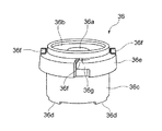
図1は、本実施の形態にかかる撮像装置の断面図である。図2は、図1の撮像装置の斜視図である。図3は、光学部材の斜視図であり、図4は、光学部材の下面図である。図5は、撮像素子の上面図である。
【0028】
光学部材1は、プラスチック材料を用いて、図1に示すようにレンズ部と脚部とが一体成形されている。より具体的には、光学部材1は、管状の脚部1cと、脚部1cの一部としてその下端に形成された4つの当接部1dと、脚部1cの上端周囲に形成された段部1eと、脚部1cの上端を塞ぐ板状の上面部1bと、上面部1bの中央に形成された凸レンズ部1aとから一体で形成されている。尚、上面部1bの上面であって、凸レンズ部1aの周囲には、遮光性のある素材からなり、凸レンズ部1aのFナンバーを規定する第1の絞りとしての開口3aを有する絞り板3が接着等により固定されている。
【0029】
光学部材1の外側には、遮光性のある素材からなる鏡枠4が配置されている。鏡枠4は、図2から明らかなように、角柱状の下部4aと、円筒状の上部4bとを設けている。下部4aの下端は、基板PC上に当接し、接着剤Bにより固着されている。下部4aの上面は、隔壁4cにより周辺側が覆われており、隔壁4cの円形内周面には、光学部材1の脚部1cが密着的に嵌合している。従って、基板PCと鏡枠4とを、例えば自動組立機に備えられた光学センサ(不図示)などを用いて、隔壁4cの円形開口部中心と、後述する撮像素子2bの光電変換部2dの中心を一致させるように位置決め配置するだけで、後述する撮像素子2bの光電変換部2dに対してレンズ部1aを、光軸直交方向に精度良く位置決めすることができる。
【0030】
一方、鏡枠4の上部4bの上端には、遮光板5が接着剤Bにより取り付けられている。遮光板5は、その中央に第2の絞りとしての開口5aを有している。遮光板5の開口5aの下方には、赤外線吸収特性を有する素材からなるフィルタ7が、接着剤Bにより取り付けられている。遮光板5とフィルタ7とでカバー部材を構成する。
【0031】
図1において、遮光板5と、光学部材1の段部1eとの間には、コイルばねからなる弾性手段6が配置され、遮光板5が鏡枠4に取り付けられることで弾性変形し、その弾性力により、光学部材1を図1中、下方に向かって押圧している。よって、遮光板5からの力は、鏡枠4を介して基板PCには伝達されるものの、直接、撮像素子2bに伝達されることがない。
【0032】
図5において、撮像ユニット2は、CMOS型イメージセンサーなどの撮像素子2bからなる。矩形薄板状の撮像素子2bの下面は、基板PCの上面に取り付けられている。撮像素子2bの上面中央には、画素が2次元的に配列された光電変換部2dが形成されており、その周囲には、撮像素子2bの内部であって且つ内側に画像処理回路が構成されている周囲面2aが形成されている。薄い側面に直交するように交差した周囲面2aの外縁近傍には、多数のパッド2cが配置されている。結線用端子であるパッド2cは、図1に示すごとくワイヤWを介して、基板PCに接続されている。ワイヤWは、基板PC上の所定の回路に接続されている。
【0033】
更に、光学部材1の当接部1dは、図4に示すごとき形状で、脚部1cの下端から突出し脚部1cの一部を構成してなる。本実施の形態においては、図5で点線に示すように、撮像素子2bの周囲面2aにおいて、パッド2cの内側に、当接部1dのみが当接した状態で配置されることとなる。従って、面平面度に関しては、当接部1dの下面のみ所定範囲に維持されれば足りる。又、脚部1c(当接部1d)は4本であって、光学部材1の重心はその中央に来るため、光学部材1を単体で平面に載置したときに、レンズ部1aの光軸が平面に対して直交するような位置と形状とを有しているといえる。従って、鏡枠4の内周面と光学部材1の外周面との間にスキマがあったとしても、撮像素子2bの周囲面2aに脚部1cを当接させたときに、撮像素子2bの光電変換部2dに対して光軸が直交し、よりひずみの少ない画像を得ることができる。ここで、周囲面2aの裏側(図1で下面側)には、撮像素子の不図示の回路(信号処理回路を含む)が設けられているが、当接部1dの当接により回路の処理には影響が及ばないようになっている。
【0034】
ここで、当接部1dの当接位置を検討するに、例えば図5に示す光電変換部2dの表面のうち、隅部2gなどは、有効画素領域を全画素領域よりやや小さめにすることで、画像形成に無関係な領域となるので、そのような場合は光電変換部2d表面内であっても、隅部2gの領域に当接部1dを当接させても撮像素子2bの撮像性能に影響を与える恐れは少ないといえる。尚、周囲面2a又は光電変換部2d表面のいずれの領域に当接させるにしろ、当接部1dからの荷重は500g以下であることが好ましい。この荷重を越えると、撮像素子2bにダメージが付与される恐れがあるからである。但し、振動などによる画像のブレを考慮すると、当接部1dからの荷重は、5g以上であることが望ましい。かかる荷重は、後述するように弾性手段であるコイルばね6の線径・巻数などを選択することにより、適切に管理することができる。また、5g以上500g以下の何れの荷重においても、面圧では1000mg/mm2以下であることが撮像素子への局所的な極度の負荷による損傷を防止する上でより好ましい。ここで、面圧とは、光学部材の脚部(当接部1d)を介して撮像素子に加えられる荷重を、その脚部が当接されているレンズ部に向いた面の面積で割ったものである。
【0035】
本実施の形態によれば、当接部1dが、撮像素子2bの周囲面2aに当接した状態で、光学部材1の段部1eの下面と、鏡枠4の下部4aの隔壁4cとの間には、スキマΔが形成されるようになっているので、レンズ部1aと撮像素子2bの光電変換部2dとの距離L(即ち光軸方向の位置決め)は、脚部1cの長さにより精度良く設定されるようになっている。本実施の形態では、4ヶ所の当接部を設けてはいるが、1ヶ所乃至3ヶ所でもよい。また、パッド2cとの干渉が回避できるのであれば、光学部材1の円筒状の脚部1cに沿った、輪帯状の当接部であっても良い。
【0036】
又、光学部材1をプラスチック材料で構成しているので、温度変化時のレンズ部の屈折率変化に基づく合焦位置のずれを低減することも可能である。すなわち、プラスチックレンズは温度が上昇するにつれて、レンズの屈折率が下がり、合焦位置がレンズから離れる方向に変化する。一方、脚部1cは温度上昇により伸びるため、合焦位置ずれの低減効果がある。尚、本実施の形態の光学部材1は、比重が比較的軽いプラスチック材料からなるので、同一体積でもガラスに比べて軽量であり、かつ衝撃吸収特性に優れるため、撮像装置を誤って落としたような場合でも、光学部材1およびそれが当接される撮像素子2bの破損を極力抑制できるという利点がある。
【0037】
又、図5に示すように、光学部材1が鏡枠4の中で任意に回転できる構造であると、当接部1dがパッド2cと干渉してしまうので、回転が規制されながら組付けられる構造(例えば回転ストッパを鏡枠4に設けるなど)が好ましい。
【0038】
本実施の形態の動作について説明する。光学部材1のレンズ部1aは、被写体像を、撮像素子2bの光電変換部2dに結像する。撮像素子2bは、受光した光の量に応じた電気的信号を画像信号等に変換しパッド2cおよびワイヤWを介して出力できるようになっている。
【0039】
更に、本実施の形態においては、光学部材1を基板PC上に取り付けるのではなく、撮像素子2bの周囲面2a上に取り付けているので、光学部材1の脚部1c(当接部1dを含む)の寸法精度、即ち、上述した距離Lの精度を管理することで、組み付け時に、レンズ部1aの合焦位置に関する調整を不要とできる。本発明の実施の形態にかかる撮像装置は、被写体距離に応じたピント調整機構が無いため、撮像装置のレンズとしては、遠距離被写体から近距離被写体までピントが合う、パンフォーカスレンズである必要がある。従って、過焦点距離U≒f2/(F×2P)(ただし、f:レンズの焦点距離、F:レンズのFナンバー、P:撮像素子の画素ピッチ)における、レンズ部1aの像点位置と、撮像素子2bの光電変換部2dとの光軸方向の位置を一致させることにより、幾何光学的には、無限遠方からU/2の距離の物体にピントが合っているとみなせる状態となる。例えば、f=3.2mm、F=2.8、P=0.0056mmの場合、基準被写体距離として、過焦点距離U≒f2/(F×2P)=0.33mにおけるレンズ部1aの像点位置と、撮像素子2bの光電変換部2dとの光軸方向の位置を一致させるように、上述の距離Lを設定すれば、無限遠方から約0.17mの距離までピントが合っている状態になる。また、必ずしも過焦点距離を基準被写体距離とする必要は無く、例えばより遠方の画質に重点を置きたい場合は、基準被写体距離を過焦点距離より遠方に設定すればよい(具体的には上述の距離Lを若干短めにすればよい。)。ここで、距離Lの精度であるが、パンフォーカスレンズとして合焦位置の調整を不要とするためには、撮像装置2bの光電変換部2dと、レンズ部1aの基準被写体距離における像点の光軸方向のズレを、空気換算長で±0.5×(F×2P)(F:撮影レンズのFナンバー、P:撮像素子の画素ピッチ)程度に抑える必要がある。また、望ましくは±0.25×(F×2P)程度に抑えるのがよい。このズレが大きいと、無限遠方や至近距離における画質が劣化してしまい好ましくない。
【0040】
又、本実施の形態によれば、光学部材1の脚部1cの当接部1dが、撮像素子2bの周囲面2aに当接することで、レンズ部1aと撮像素子2bの光電変換部2dとの光軸方向の位置決めを行うことができる。又、鏡枠4が、基板PCに撮像素子2bの光電変換部2dを位置決め基準にして設置されることで、レンズ部1aと撮像素子2bの光電変換部2dとの光軸直交方向の位置決めが行われるので、低コストでありながら高い位置決め精度を達成できることとなる。
【0041】
特に、撮像素子2bの周囲面2aに、撮像素子2bと基板PCとを接続するためのパッド2c及びワイヤWが形成されているような場合、脚部1cの当接部1dが、パッド2cよりも光電変換部2d側において周囲面2aに当接するように構成すれば、撮像素子2bをコンパクトな構成に維持しつつも、当接部1dの当接面積を大きく確保でき、それにより光学部材1を安定化させると共に、当接面の面圧を低く抑えることができるため、撮像素子2bの保護を図りながらも、パッド2cやワイヤWとの干渉が抑制され、しかも高精度の位置決めが達成されることとなる。尚、鏡枠4が基板PCに接着されており、他の2ヶ所の接着部とあわせて、撮像装置の外部に対して、異物が侵入しないよう密封された状態に維持されるため、撮像素子2bの光電変換部2dに対する異物の悪影響を排除することができる。これらに用いる接着剤は、防湿性を有するのが好ましい。これにより、湿気の侵入による撮像素子やパッドの表面劣化を防ぐことができる。
【0042】
更に、光学部材1の段部1eを、所定の弾性力で光軸方向に押圧する弾性手段6を設けているので、かかる弾性手段6の弾性力を用いて、鏡枠4に対して光軸方向に沿って、脚部1c(当接部1d)を撮像素子2bの周囲面2aに適切な当接力(上述した5g以上500g以下の荷重に相当する力)で押しつけることができ、従って光学部材1と撮像素子2bとの光軸方向の位置決めが容易であるにもかかわらず、経時変化により部品に反りなどの変形が生じたような場合にも、安定した弾性力で、光学部材1を撮像素子2bに対して付勢することができ、それにより振動が生じた際における光学部材1のガタつきを抑えることができ、しかも衝撃が生じた際に、内側に回路が配置された撮像素子2bの周囲面2aに過大なストレスを生じさせることがない。また、鏡枠4の光軸方向に衝撃力などの大きな力が加わった場合でも、その力は鏡枠4を介して基板PCには伝達されるが、直接撮像素子2bに伝達されることはなく、撮像素子2bの保護という観点から好ましい。尚、弾性手段6としては、ウレタンやスポンジなども考えられるが、長期間安定した弾性力を発揮できる金属製のばねなどが好ましい。
【0043】
又、遮光板5とフィルタ7とで構成するカバー部材を、レンズ部1aより被写体側に配置しているので、レンズ部1aを剥き出しにすることなく、その保護が図れると共に、レンズ面への異物の付着防止も図れる。更に、フィルタ7が、赤外線吸収特性を有する材質から形成されているので、別個に赤外線カットフィルタを設ける必要がなくなり、部品点数を削減できるため好ましい。フィルタ7に赤外線カット特性を付与する代わりに、光学部材1自体を赤外線吸収特性のある素材から形成したり、レンズ1aの表面に、赤外線カット特性を有する皮膜をコーティングしてもよい。
【0044】
更に、組み付け時において、遮光板5を鏡枠4から取り外した状態で、光学部材1を、鏡枠4に対して被写体側より挿入することができ、その後、遮光板5を鏡枠4に組み付けることができる。このような構成により、光学部材1の組み付け性が向上し、自動組立などを容易に行うことができる。この際に、鏡枠4の下部4aいずれかに空気逃げの孔を形成しておくと、鏡枠4と光学部材1とのスキマがわずかであっても、容易に組み付けを行うことができる。但し、かかる空気逃げの孔は、組み付け後に充填剤などで封止することによって、外部からの異物の侵入や、湿気による撮像素子およびパッドの表面劣化などを抑制することが好ましい。また、かかる場合の充填剤は、光漏れを抑制するように遮光性のあるものが好ましい。尚、基板PCに鏡枠4を接着した後に、光学部材1を挿入しても良く、或いは光学部材1を鏡枠4に取り付けた後に、そのユニット毎基板PCに接着するようにしても良く、それにより工程の自由度が確保される。後者の組付手順とする場合は、鏡枠4の隔壁4cは光学部材1の抜け落ち防止の機能をかねることができる。
【0045】
光学部材1の脚部1cが、撮像素子2bの光電変換部2dの近くに配置されているため、結像に寄与しない光束が脚部1cに反射し、光電変換部2dに入射することで、ゴーストやフレアが生じる原因となることが懸念される。これを防止するには、レンズ部1aのFナンバーを規定する第1の絞り(開口3a)の被写体側に、周辺光束を規制する第2の絞り(開口5a)を配置し、不要光の入射を低減させるのが効果的である。なお、撮像素子2bの光電変換部2dの短辺・長辺、対角方向で画角が異なるため、第2の絞りの開口5aを矩形とすることで、より一層の効果が得られる。更に、本実施の形態では、遮光板5の開口5aにこの機能を持たせているが、フィルタ7の被写体側に、遮光性を有する被膜を必要な開口部以外にコーティングもしくは塗布することで絞りを形成してもよい。又、同様な理由により、脚部1cの少なくとも一部に内面反射防止処理を施すのが好ましい。内面反射防止処理とは、例えば微小な凹凸を設けた面を形成し、結像に寄与しない光束を散乱させるようにすること、反射防止コーティングまたは低反射特性を有する塗料を塗布することを含む。
【0046】
又、開口3aを備えた絞り板3をレンズ部1aの入射面側に設けているので、撮像素子2bの受光面2dに入射する光束を、垂直に近い角度で入射させ、すなわちテレセントリックに近いものとすることができ、それにより高画質な画像を得ることができる。更に、レンズ部1aの形状は、像側に強い曲率の面を向けた正レンズの形状とすることで、第1の絞り(開口3a)とレンズ部1aの主点との間隔が大きくとれ、よりテレセントリックに近い望ましい構成となる。本実施の形態では、レンズ部1aを像側に凸面を向けた正のメニスカス形状としている。また、より高画質な画像を得るためには、後述する第3の実施の形態のごとく、レンズ部を複数枚のレンズで構成するのが好ましい。
【0047】
図7は、弾性手段の変形例を含む撮像装置の断面図であり、図8は、光学部材と弾性手段とを分解した状態で示す斜視図である。図7の弾性手段16は、遮光性を有する素材からなり、図1の絞り板3の代わりに絞り機能を発揮するようになっている。より具体的に説明すると、図8から明らかなように、樹脂製の弾性手段16は、中央に開口(絞り)16aを有する略円盤状のシート状部材であって、その円周から等間隔に半径方向外方に向かって4つの突起部16bが突出している。一方、光学部材の頂部に形成されたリング部11fは、突起部16bに対応して、切欠11gを形成している。切欠11gに突起部16bを係合させることで、弾性手段16は、リング部11f内に嵌合的に取り付けられるようになっている。更に、遮光板15を取り付ける際に、その下面に形成された突起15cで、各突起部16bを上方から押圧すると、突起部16bが弾性変形し、光学部材11を所定の弾性力で撮像素子2bの周囲面2aに対して付勢するようになっている。その他の構成に関しては、図1に示す実施の形態と同様であるので、説明を省略する。
【0048】
図9は、第2の実施の形態にかかる撮像装置を示す図である。第2の実施の形態においては、上述した実施の形態に対して、絞り板及び遮光板の構成を変更した点のみが異なるため、その他の同様な構成に関しては、同一符号を付して説明を省略する。
【0049】
図9において、鏡枠4の上部4bの上端には、薄い遮光シート8を上面に貼り付けた保持部材5’が、接着剤Bにより取り付けられている。遮光性のある素材からなる保持部材5’の中央の開口5a’内には、赤外線吸収特性を有する素材からなるフィルタ7’が嵌合配置されている。保持部材5’の開口5a’の上縁には、テーパ面5b’が形成されており、ここに接着剤Bを付着させることによって、保持部材5’とフィルタ7’との接合を行うことができる。更に、保持部材5’は、開口5a’の下方に向かって突出し内径が段々と縮径する縮径部5c’を設けており、その下端の最も絞られた部分が、第1の絞り5d’を構成する。又、遮光シート8の中央開口8aが第2の絞りを構成する。保持部材5’とフィルタ7’と遮光シート8とでカバー部材を構成する。
【0050】
本実施の形態によれば、保持部材5’とフィルタ7’と遮光シート8とで構成するカバー部材を、光学部材1のレンズ部1aより被写体側に配置しているので、レンズ部1aを剥き出しにすることなく、その保護が図れると共に、レンズ面への異物の付着防止も図れる。更に、かかるカバー部材は一体で形成できることから、撮像装置全体の部品点数の削減に貢献する。
【0051】
上述の実施の形態と同様に、光学部材1の脚部1cが、撮像素子2bの光電変換部2dの近くに配置されているため、結像に寄与しない光束が脚部1cに反射し、光電変換部2dに入射することで、ゴーストやフレアが生じる原因となることが懸念される。本実施の形態においては、レンズ部1aのFナンバーを規定する第1の絞り5a’の被写体側に、周辺光束を規制する第2の絞り(開口8a)を配置し不要光の入射を低減している。なお、撮像素子2bの光電変換部2dの短辺・長辺、対角方向で画角が異なるため、第2の絞りの開口8aを矩形とすることで、より一層の効果が得られる。
【0052】
更に、本実施の形態においても、光学部材1の段部1eを、所定の弾性力で光軸方向に押圧する、付勢部材としての弾性手段6を設けているので、かかる弾性手段6の弾性力を用いて、鏡枠4に対して光軸方向に沿って、脚部1c(当接部1d)を撮像素子2bの周囲面2aに適切な当接力(上述した5g以上500g以下の当接力)で押しつけることができ、従って内側に回路が配置された撮像素子2bの周囲面2aに過大なストレスを生じさせることがないし、振動で光学部材1ががたつくこともないようになっている。
【0053】
図10は、弾性手段の別な変形例を含む撮像装置の断面図である。図10の弾性手段26は、保持部材すなわちカバー部材と一体になっている。図10から明らかなように、保持部材26は、エラストマー樹脂等の弾性変形しやすい樹脂材料からなり、図9の弾性手段6を取り除き、図9の保持部材5’に対して、下面に等間隔に4つ(2つのみ図示)の突起部(弾性手段)26eを形成した点のみが異なっている。保持部材26を鏡枠4に接着剤Bにより固着し、突起部26eが弾性変形することにより、光学部材1を所定の弾性力で撮像素子2bの周囲面2aに対して付勢するようになっている。その他の構成に関しては、図9に示す実施の形態と同様であるので、説明を省略する。
【0054】
図11は、第3の実施の形態にかかる撮像装置を示す図である。第3の実施の形態においては、図2の実施の形態に対して、複数のレンズ部を有するように光学部材の構成を変更した点のみが主として異なるため、脚部と撮像素子との当接位置を含む、その他の同様な構成に関しては、同一符号を付して説明を省略する。
【0055】
図11において、光学部材19は、それぞれプラスチック材料からなる像側レンズ1’と被写体側レンズ9とから構成されている。像側レンズ1’は、図1に示す光学部材1と類似の形状を有しているが、上部に形成されたリング部1f’の光軸方向高さが増大している。リング部1f’の半径方向内側であって上面部1b’の上方には、Fナンバーを規定する絞り板3を介して被写体側レンズ9が配置されている。被写体側レンズ9は、リング部1f’の内周に嵌合するフランジ部9bと、中央に形成されたレンズ部9aとから構成されている。像側レンズ1’のレンズ部1a’が正のレンズであるのに対し、被写体側レンズ9のレンズ部9aは、負のレンズとなっている。尚、本実施の形態では絞り板3は、レンズ部1a’、9aのレンズ間距離を規制するスペーサとして機能し、且つ絞り板3の開口3aがFナンバーを規定する第1の絞りとして機能する。
【0056】
像側レンズ1’のリング部1f’の内周面と、被写体側レンズ9のフランジ部9bの外周面とは、互いに同径であり且つ光軸に平行になっているので、かかる面同士が係合することにより、レンズ部1a’、9aの光軸直交方向の位置決めを行うことができ、それらの光軸を容易に一致させることができる。尚、像側レンズ1’に対して、被写体側レンズ9は、その周囲に付与された接着剤Bにより接合されている。
【0057】
鏡枠4の上部4bの上端には、薄い遮光シート8を上面に貼り付けた保持部材5’が、接着剤Bにより取り付けられている。遮光性のある素材からなる保持部材5’の中央の開口5a’内には、赤外線吸収特性を有する素材からなるフィルタ7’が嵌合配置されている。保持部材5’の開口5a’の上縁には、テーパ面5b’が形成されており、ここに接着剤Bを付着させることによって、保持部材5’とフィルタ7’との接合を行うことができる。更に、保持部材5’は、開口5a’の下方に向かって突出し内径が段々と縮径する縮径部5c’を設けているが、かかる部分は、不要光の侵入を抑制する遮光部として機能する。尚、遮光シート8の中央開口8aが第2の絞りを構成する。
【0058】
更に、本実施の形態においても、光学部材19の段部1e’を、所定の弾性力で光軸方向に押圧する、付勢部材としての弾性手段6を設けているので、かかる弾性手段6の弾性力を用いて、鏡枠4に対して光軸方向に沿って、脚部1c’(当接部1d’)を撮像素子2bの周囲面2aに適切な当接力(上述した5g以上500g以下の当接力)で押しつけることができ、従って内側に回路が配置された撮像素子2bの周囲面2aに過大なストレスを生じさせることがないし、振動で光学部材19ががたつくこともないようになっている。
【0059】
図12は、弾性手段の更に別な変形例の斜視図である。図12の弾性手段36は、光学部材と一体になっており、例えば弾性手段6を省略した図1の撮像装置に組み込み可能なものである。図12から明らかなように、光学部材36は、図1の光学部材1に対して、段部36eに、等間隔に4つ(3つのみ図示)の突起部(弾性手段)36fと、それを支持するアーム部36gを形成した点のみが異なっている。図1に示すごとく光学部材36を組み付けた状態では、突起部36gが遮光板5(図1)の下面に当接するようになっており、それにより片持ちのアーム36gが弾性変形し、その結果生じる弾性力により、光学部材1を所定の弾性力で撮像素子2bの周囲面2aに対して付勢するようになっている(図1)。その他の構成に関しては、図1に示す実施の形態と同様であるので、説明を省略する。
【0060】
図13は、弾性手段の更に別な変形例を含む撮像装置の断面図である。図13の弾性手段は、鏡枠と一体になっている。図13から明らかなように、鏡枠46は、図1の鏡枠4に対して、上半部46bに、等間隔に4つ(2つのみ図示)の切欠46dを形成しており、かかる切欠46dの図13で下縁に、光軸に平行に延在するアーム46eの下端を接続している。アーム46eの上端には、光軸直角方向内向きに突出した、断面が略三角形状の突起部46fが形成されている。尚、光学部材1の段部1eの上部は、図13に示すようにテーパ形状となっていると好ましい。アーム46eと突起部46fとで弾性手段を構成する。
【0061】
基板PCに取り付けられた鏡枠46内に、光学部材1を図13の上方から挿入する際は、突起部46fに段部1eが当接して、アーム46eを光軸直角方向外向きに押し広げるように弾性変形させるため、光学部材1の組み込みは容易である。一方、図13に示す位置まで、光学部材1が組み付けられたときは、アーム46eの変形が復帰するが、その復帰は完全ではなく若干変形が残るように突起部46fの形状が決められている。従って、その結果生じる弾性力により、突起部46fは、矢印の方向に段部1eを付勢し、それにより光学部材1を所定の弾性力で撮像素子2bの周囲面2aに対して付勢するようになっている。その他の構成に関しては、図1に示す実施の形態と同様であるので、説明を省略する。尚、本実施の形態においては、アーム46eと突起部46fを形成する構造上、このままでは十分な防塵・防湿機能を発揮することができない。これに対し、たとえば鏡枠46の弾性構造部(46e、46f)のスキマを別部材で覆うことにより所望の防塵・防湿機能を発揮させることができる。
【0062】
更に、弾性手段の他の例としては、以上述べた他にも、波ばねや、皿ばねの組み合わせを用いても良い。
【0063】
以上、本発明を実施の形態を参照して説明してきたが、本発明は上記実施の形態に限定して解釈されるべきではなく、適宜変更・改良が可能であることはもちろんである。例えば、本実施の形態では、撮像素子2bと基板PCとの接続は、ワイヤWにより行っているが、撮像素子2bの内部に配線をはわせて、撮像素子2bの背面(光電変換部と反対側)又は側面より、信号を取り出す構成であってもよい。かかる構成によれば、撮像素子の周囲面を広く確保できると共に、結線を容易に行うことができる。更に、本実施の形態では、撮像素子をベアチップのみから構成したが、その上面又は下面にガラスなどの保護部材を張り付けることで、一体形の撮像素子を構成することでき、そのような撮像素子を用いてもよい。又、基板は、ハードなものに限らず、フレキシブルなものであっても良い。脚部を撮像素子のレンズ部に向いた面に当接する態様にすることが、レンズの像点位置に適合するように、撮像素子に当接される脚部の長さ寸法を適宜設計することで、無調整であっても精度良く組み付けできる信頼性の高い撮像装置を得ることができる上で特に好ましいものである。本発明の撮像装置は、携帯電話、パソコン、PDA、AV装置、テレビ、家庭電化製品など種々のものに組み込むことが可能である。
【0064】
【発明の効果】
本発明によれば、安価でありながら、部品点数を削減でき、小型化が図れ、長期にわたってレンズのがたつきや外力による損傷を抑制でき、また更に、無調整であっても精度良く組み付けでき、さらには防塵、防湿の構造を有し、また信頼性の高い撮像装置を提供することができる。
【図面の簡単な説明】
【図1】第1の実施の形態にかかる撮像装置の断面図である。
【図2】図1の撮像装置の斜視図である。
【図3】光学部材の斜視図である。
【図4】光学部材の下面図である。
【図5】撮像素子の上面図である。
【図6】従来技術の撮像装置の一例を示す断面図
【図7】弾性手段の変形例を含む撮像装置の断面図である。
【図8】光学部材と弾性手段とを分解した状態で示す斜視図である。
【図9】第2の実施の形態にかかる撮像装置の断面図である。
【図10】弾性手段の別な変形例を含む撮像装置の断面図である。
【図11】第3の実施の形態にかかる撮像装置の断面図である。
【図12】弾性手段の別な変形例の斜視図である。
【図13】弾性手段の別な変形例を含む撮像装置の断面図である。
【符号の説明】
1、11、19、36 光学部材
1a、1a’ レンズ部
1c 脚部
1d 当接部
2 撮像ユニット
2a 周囲面
2b 撮像素子
2d 光電変換部
3 絞り板
4、46 鏡枠
5、15 遮光板
6 弾性手段
7 フィルタ
8 遮光シート
9 被写体側レンズ
9a レンズ部
16 弾性部材
1’ 像側レンズ
5’、26 保持部材
7’ フィルタ[0001]
BACKGROUND OF THE INVENTION
The present invention relates to an imaging apparatus, and more particularly to an imaging apparatus that can be installed in a mobile phone, a personal computer (personal computer), or the like.
[0002]
[Prior art]
In recent years, it has become possible to easily handle digital image data due to higher performance of CPUs and development of image processing technology. In particular, since mobile phones and PDAs are available with a display equipped with a display capable of displaying images and in the near future, a dramatic improvement in wireless communication speed can be expected, image data between such mobile phones and PDAs can be expected. Transfers are expected to occur frequently.
[0003]
By the way, currently, after converting a subject image into image data with a digital still camera or the like, such image data is transferred via the Internet via a personal computer or the like. However, in such an aspect, it is necessary to have both a digital still camera and a personal computer in order to transfer image data. On the other hand, there is an attempt to mount an image sensor such as a CCD image sensor on a mobile phone. According to such an attempt, it is not necessary to own a digital still camera or a personal computer, and an image can be easily captured and sent to a partner with a mobile phone that can be easily carried around.
[0004]
[Problems to be solved by the invention]
However, at present, if the mobile phone has the functions of a digital still camera that is much larger than a mobile phone, the mobile phone itself becomes larger and heavier and cannot be easily carried. In addition, the manufacturing cost increases accordingly.
[0005]
In particular, even if the imaging optical system, which is the main component of a digital still camera, and the imaging device are unitized, the photoelectric conversion unit of the imaging device must be set appropriately at the in-focus position of the imaging optical system. First, the problem is how to make the adjustment. For example, when the image sensor and the photographic optical system are installed on the same substrate, due to factors such as variations in the thickness of the adhesive used to attach to the substrate and dimensional variations in the components, the focus position of the photographic optical system In addition, it can be said that it is difficult to accurately assemble the photoelectric conversion portion of the imaging element. Therefore, in order to increase the focusing accuracy of the photographing optical system and the photoelectric conversion unit of the image sensor, a highly accurate assembling technique is required, or a mechanism for adjusting the focusing position separately is required. If it does so, there exists a problem that manufacturing cost rises. An example is given to point out the problems of the prior art.
[0006]
FIG. 6 is a cross-sectional view showing an example of a conventional imaging apparatus, in which an
[0007]
A
[0008]
The upper portion of the
[0009]
As described above, the imaging device of the prior art is a relatively large device composed of a large number of parts. Therefore, it takes time to assemble these parts while avoiding the above-mentioned problem of manufacturing cost. It is also necessary to adjust the relative position between the
[0010]
In order to solve such problems, the lens is provided with a leg portion extending to the vicinity of the focal length position of the lens, and an attempt is made to configure the imaging apparatus by directly contacting the leg portion with the imaging element. There is an attempt to do. According to such an attempt, it is possible to arrange the photoelectric conversion unit of the image sensor at the in-focus position of the lens, and it is possible to greatly reduce the labor when assembling the imaging device.
[0011]
However, in various devices equipped with such a compact imaging device, it is expected that vibrations, impacts when accidentally dropped, and the like are applied. In such a case, if the leg portion of the lens is in contact with the image pickup device, the lens may become loose due to vibration or the image pickup device may be damaged by an impact.
[0012]
In order to solve such a problem, it is also conceivable that the lens is brought into contact with the image pickup element while applying a predetermined pressure by the lens holder, and is fixed by adhering the lens holder and the substrate (Japanese Patent Laid-Open No. Hei 9- No. 284617). According to such a technique, the rattling between the lens and the image sensor can be suppressed, but if the pressure is reduced due to the change in the thickness of the adhesive or the shape of the part over time, the lens may be rattled. Further, there is still a possibility that the lens may damage the imaging device due to the impact force.
[0013]
The present invention has been made in view of such problems, and while being inexpensive, the number of parts can be reduced, the size can be reduced, and lens damage and damage due to external force can be suppressed over a long period of time. An object of the present invention is to provide a highly reliable image pickup apparatus that can be assembled with high precision even without adjustment and that has a dustproof and moistureproof structure.
[0014]
[Means for Solving the Problems]
In order to achieve such an object, an imaging device according to a first aspect of the present invention includes an imaging device including a photoelectric conversion unit configured by a bare chip alone, or a protective member attached to an upper surface or a lower surface of the bare chip, and the imaging device. , A lens unit that forms a subject image on the photoelectric conversion unit provided in the imaging device, a leg portion that supports the lens unit, and a contact surface that contacts the imaging device. An optical member, an elastic means, and a lens frame fixed to the substrate and supporting the optical member, and the optical member is pressed in the optical axis direction by the elastic force of the elastic means. The member is biased toward the image sensorIn the stateThe contact surface is in contact with only the surface of the image sensor facing the lens portion.
[0015]
An image pickup apparatus according to a second aspect of the present invention includes an image pickup device including a photoelectric conversion unit configured by a bare chip alone, or a protective member attached to an upper surface or a lower surface of the bare chip, a substrate on which the image pickup device is attached, An optical member including a lens unit that forms a subject image on the photoelectric conversion unit provided in the image sensor, a leg unit that supports the lens unit, and a contact surface that contacts the image sensor, and the substrate A lens frame that is fixed to the optical member and supports the optical member and includes elastic means, and the optical member is pressed in the optical axis direction by the elastic force of the elastic means, so that the optical member captures the image Energize towards the elementIn the stateThe contact surface is in contact with only the surface of the image sensor facing the lens portion.
[0016]
[Action]
An image pickup apparatus according to a first aspect of the present invention includes an image pickup device including a photoelectric conversion unit configured by a bare chip alone, or a protective member attached to an upper surface or a lower surface of the bare chip, a substrate on which the image pickup device is attached, An optical member including a lens unit that forms a subject image on the photoelectric conversion unit included in the image sensor; a leg unit that supports the lens unit; and a contact surface that contacts the image sensor; and elastic means And a lens frame that is fixed to the substrate and supports the optical member, and the optical member is directed toward the imaging element by pressing the optical member in the optical axis direction by the elastic force of the elastic means. EnergizingIn the stateSince the abutment surface abuts only on the surface of the image sensor facing the lens portion, a stable elastic force can be obtained even when the part is warped or deformed due to changes over time. Thus, the optical member can be biased with respect to the image pickup device, whereby the distance in the optical axis direction between the lens unit and the image pickup device is always maintained constant, and the vibration is generated when vibration occurs. The play of the optical member can be suppressed, and damage to the image sensor when an impact occurs can be suppressed. The image sensor is preferably a CMOS (Complementary Metal Oxide Semiconductor) image sensor, but may be a CCD (Charged Coupled Device) image sensor.
[0017]
Further, when the leg portion is in contact with the surface of the imaging device facing the lens portion with a load of 5 g or more and 500 g or less due to the elastic force of the elastic means, the imaging is performed by appropriate management of the elastic force. Damage to the element can be suppressed.
[0018]
or,Mirror frameThe lens unit can be protected if it has a cover member that is disposed on the subject side with respect to the lens unit, presses the elastic means, and has at least a part that can transmit light. That is, because of the cover member, the lens portion is not exposed to the outside, and the impact to the cover member from the outside is absorbed by the elastic member, so that a strong impact is applied to the lens portion. As a result, the image sensor is prevented from being damaged.
[0019]
Furthermore, when the elastic means is configured separately from the optical member and the cover member, only the elastic means needs to be replaced when managing the elastic force, and the cost can be reduced. Here, the separate body is composed of individual independent members, is not integrated with an adhesive or the like, and is in a state where it can be handled as individual parts when removed.
[0020]
Further, when the elastic means is a coil spring, the elastic force can be exerted stably for a long time.
[0021]
Further, if the elastic means is a sheet-like member having an opening in the center, it is easy to assemble and is preferable from the viewpoint of space saving.
[0022]
In addition, the sheet-like member is made of a light-shielding member, and it is preferable that the sheet-like member also serves as a diaphragm for defining the F number of the lens unit because it is not necessary to provide a diaphragm separately, and the number of parts is reduced.
[0023]
On the other hand, it is preferable that the elastic means is integrated with the cover member because the number of parts is reduced.
[0024]
Further, it is preferable that the elastic means is integrated with the optical member because the number of parts is reduced.
Furthermore, it is preferable that the lens frame is fixed to the substrate.
[0025]
An image pickup apparatus according to a second aspect of the present invention includes an image pickup device including a photoelectric conversion unit configured by a bare chip alone, or a protective member attached to an upper surface or a lower surface of the bare chip, a substrate on which the image pickup device is attached, An optical member including a lens unit that forms a subject image on the photoelectric conversion unit provided in the image sensor, a leg unit that supports the lens unit, and a contact surface that contacts the image sensor, and the substrate A lens frame that is fixed to the optical member and supports the optical member and includes elastic means, and the optical member is pressed in the optical axis direction by the elastic force of the elastic means, so that the optical member captures the image Energize towards the elementIn the stateSince the abutment surface abuts only on the surface of the image sensor facing the lens portion, a stable elastic force can be obtained even when the part is warped or deformed due to changes over time. Thus, the optical member can be biased with respect to the image pickup device, whereby the distance in the optical axis direction between the lens unit and the image pickup device is always maintained constant, and the vibration is generated when vibration occurs. The play of the optical member can be suppressed, and damage to the image sensor when an impact occurs can be suppressed.
[0026]
Further, when the leg portion is in contact with the surface of the imaging device facing the lens portion with a load of 5 g or more and 500 g or less due to the elastic force of the elastic means, the imaging is performed by appropriate management of the elastic force. Damage to the element can be suppressed.
[0027]
DETAILED DESCRIPTION OF THE INVENTION
Embodiments of the present invention will be described below with reference to the drawings.
FIG. 1 is a cross-sectional view of the imaging apparatus according to the present embodiment. FIG. 2 is a perspective view of the imaging apparatus of FIG. FIG. 3 is a perspective view of the optical member, and FIG. 4 is a bottom view of the optical member. FIG. 5 is a top view of the image sensor.
[0028]
As shown in FIG. 1, the
[0029]
A
[0030]
On the other hand, a
[0031]
In FIG. 1, an
[0032]
In FIG. 5, the
[0033]
Furthermore, the
[0034]
Here, in order to examine the contact position of the
[0035]
According to the present embodiment, the
[0036]
Further, since the
[0037]
Further, as shown in FIG. 5, if the
[0038]
The operation of this embodiment will be described. The
[0039]
Further, in the present embodiment, the
[0040]
In addition, according to the present embodiment, the
[0041]
In particular, when the
[0042]
Further, since the
[0043]
Further, since the cover member composed of the
[0044]
Further, the
[0045]
Since the
[0046]
Further, since the
[0047]
FIG. 7 is a cross-sectional view of an imaging apparatus including a modification of the elastic means, and FIG. 8 is a perspective view showing the optical member and the elastic means in an exploded state. The elastic means 16 in FIG. 7 is made of a light-shielding material, and exhibits a diaphragm function instead of the
[0048]
FIG. 9 is a diagram illustrating an imaging apparatus according to the second embodiment. The second embodiment is different from the above-described embodiment only in that the configurations of the diaphragm plate and the light shielding plate are changed. Therefore, the other similar configurations are denoted by the same reference numerals and described. Omitted.
[0049]
In FIG. 9, a holding
[0050]
According to the present embodiment, the cover member constituted by the holding
[0051]
Similar to the above-described embodiment, the
[0052]
Further, in the present embodiment, since the
[0053]
FIG. 10 is a cross-sectional view of an imaging apparatus including another modification of the elastic means. The elastic means 26 in FIG. 10 is integrated with a holding member, that is, a cover member. As is apparent from FIG. 10, the holding
[0054]
FIG. 11 is a diagram illustrating an imaging apparatus according to the third embodiment. The third embodiment is mainly different from the embodiment of FIG. 2 only in that the configuration of the optical member is changed so as to have a plurality of lens portions. Other similar configurations including the position are denoted by the same reference numerals and description thereof is omitted.
[0055]
In FIG. 11, the
[0056]
The inner peripheral surface of the
[0057]
A holding
[0058]
Further, in the present embodiment, since the
[0059]
FIG. 12 is a perspective view of still another modified example of the elastic means. The elastic means 36 of FIG. 12 is integrated with the optical member, and can be incorporated into the imaging apparatus of FIG. 1 in which the
[0060]
FIG. 13 is a cross-sectional view of an imaging apparatus including still another modified example of the elastic means. The elastic means of FIG. 13 is integrated with the lens frame. As is apparent from FIG. 13, the
[0061]
When the
[0062]
Further, as another example of the elastic means, in addition to the above, a combination of a wave spring or a disc spring may be used.
[0063]
The present invention has been described above with reference to the embodiments. However, the present invention should not be construed as being limited to the above-described embodiments, and can be modified or improved as appropriate. For example, in the present embodiment, the
[0064]
【The invention's effect】
According to the present invention, while being inexpensive, the number of parts can be reduced, the size can be reduced, the lens can be prevented from rattling or damage due to external force over a long period of time, and furthermore, it can be assembled with high precision even without adjustment. In addition, it is possible to provide a highly reliable imaging device having a dustproof and moistureproof structure.
[Brief description of the drawings]
FIG. 1 is a cross-sectional view of an imaging apparatus according to a first embodiment.
2 is a perspective view of the imaging apparatus of FIG. 1. FIG.
FIG. 3 is a perspective view of an optical member.
FIG. 4 is a bottom view of the optical member.
FIG. 5 is a top view of the image sensor.
FIG. 6 is a cross-sectional view showing an example of a conventional imaging device
FIG. 7 is a cross-sectional view of an imaging apparatus including a modification of elastic means.
FIG. 8 is a perspective view showing an optical member and elastic means in an exploded state.
FIG. 9 is a cross-sectional view of an imaging apparatus according to a second embodiment.
FIG. 10 is a cross-sectional view of an imaging apparatus including another modification of elastic means.
FIG. 11 is a cross-sectional view of an imaging apparatus according to a third embodiment.
FIG. 12 is a perspective view of another modified example of the elastic means.
FIG. 13 is a cross-sectional view of an imaging apparatus including another modification of elastic means.
[Explanation of symbols]
1, 11, 19, 36 Optical member
1a, 1a 'lens part
1c Leg
1d contact part
2 Imaging unit
2a Surrounding surface
2b Image sensor
2d photoelectric converter
3 Aperture plate
4, 46 Mirror frame
5, 15 Shading plate
6 Elastic means
7 Filter
8 Shading sheet
9 Subject lens
9a Lens part
16 Elastic member
1 'image side lens
5 ', 26 holding member
7 'filter
Claims (13)
前記撮像素子が取り付けられた基板と、
前記撮像素子に備えられる前記光電変換部に被写体像を結像させるレンズ部と、前記レンズ部を支持する脚部と、前記撮像素子に当接する当接面とを備えた光学部材と、
弾性手段と、
前記基板に固定され前記光学部材を支持する鏡枠と、を有し、
前記弾性手段の弾性力により前記光学部材を光軸方向に押圧することにより、前記光学部材は前記撮像素子に向かって付勢された状態で、前記当接面が前記撮像素子の前記レンズ部に向いた面のみに当接するようになっていることを特徴とする撮像装置。An image pickup device including a photoelectric conversion unit configured by a bare chip only, or a protective member attached to the upper or lower surface of the bare chip;
A substrate on which the image sensor is attached;
An optical member including a lens unit that forms a subject image on the photoelectric conversion unit provided in the image sensor, a leg unit that supports the lens unit, and a contact surface that contacts the image sensor;
Elastic means;
A lens frame fixed to the substrate and supporting the optical member,
By pressing the optical member in the optical axis direction by the elastic force of the elastic means, in a state wherein the optical member is urged toward the image pickup device, the said lens portion of the contact surface is the imaging device An imaging apparatus, wherein the imaging apparatus is configured to abut only on a facing surface.
前記撮像素子が取り付けられた基板と、
前記撮像素子に備えられる前記光電変換部に被写体像を結像させるレンズ部と、前記レンズ部を支持する脚部と、前記撮像素子に当接する当接面とを備えた光学部材と、
前記基板に固定され前記光学部材を支持すると共に、弾性手段を備えた鏡枠と、を有し、
前記弾性手段の弾性力により前記光学部材を光軸方向に押圧することにより、前記光学部材は前記撮像素子に向かって付勢され、前記当接面が前記撮像素子の前記レンズ部に向いた面のみに当接するようになっていることを特徴とする撮像装置。An image pickup device including a photoelectric conversion unit configured by a bare chip only, or a protective member attached to the upper or lower surface of the bare chip;
A substrate on which the image sensor is attached;
An optical member including a lens unit that forms a subject image on the photoelectric conversion unit provided in the image sensor, a leg unit that supports the lens unit, and a contact surface that contacts the image sensor;
A lens frame fixed to the substrate and supporting the optical member, and having an elastic means,
By pressing the optical member in the optical axis direction by the elastic force of the elastic means, the optical member is urged toward the imaging element, and the contact surface faces the lens portion of the imaging element. An image pickup apparatus that is configured to contact only the head.
Priority Applications (1)
| Application Number | Priority Date | Filing Date | Title |
|---|---|---|---|
| JP2002001974A JP3915513B2 (en) | 2001-01-12 | 2002-01-09 | Imaging device |
Applications Claiming Priority (7)
| Application Number | Priority Date | Filing Date | Title |
|---|---|---|---|
| JP2001-4706 | 2001-01-12 | ||
| JP2001004706 | 2001-01-12 | ||
| JP2001-33111 | 2001-02-09 | ||
| JP2001033111 | 2001-02-09 | ||
| JP2001148912 | 2001-05-18 | ||
| JP2001-148912 | 2001-05-18 | ||
| JP2002001974A JP3915513B2 (en) | 2001-01-12 | 2002-01-09 | Imaging device |
Publications (3)
| Publication Number | Publication Date |
|---|---|
| JP2003037758A JP2003037758A (en) | 2003-02-07 |
| JP2003037758A5 JP2003037758A5 (en) | 2005-01-06 |
| JP3915513B2 true JP3915513B2 (en) | 2007-05-16 |
Family
ID=27481968
Family Applications (1)
| Application Number | Title | Priority Date | Filing Date |
|---|---|---|---|
| JP2002001974A Expired - Fee Related JP3915513B2 (en) | 2001-01-12 | 2002-01-09 | Imaging device |
Country Status (1)
| Country | Link |
|---|---|
| JP (1) | JP3915513B2 (en) |
Families Citing this family (27)
| Publication number | Priority date | Publication date | Assignee | Title |
|---|---|---|---|---|
| US7391458B2 (en) | 2002-07-01 | 2008-06-24 | Rohm Co., Ltd. | Image sensor module |
| JP4645023B2 (en) * | 2003-05-30 | 2011-03-09 | コニカミノルタオプト株式会社 | Imaging device and portable terminal equipped with the same |
| EP1643282A4 (en) * | 2003-07-08 | 2009-06-03 | Konica Minolta Opto Inc | Imaging device, portable terminal using the same, and image device producing method |
| JP4492085B2 (en) * | 2003-10-07 | 2010-06-30 | コニカミノルタオプト株式会社 | Imaging device and portable terminal |
| DE10344768B3 (en) * | 2003-09-26 | 2005-08-18 | Siemens Ag | Optical module with resilient element between lens holder and circuit carrier and optical system |
| JP4622237B2 (en) * | 2003-11-12 | 2011-02-02 | コニカミノルタオプト株式会社 | Imaging device and portable terminal equipped with imaging device |
| TW200527881A (en) * | 2004-01-30 | 2005-08-16 | Konica Minolta Opto Inc | Optical unit, imaging device with the optical unit and portable terminal with the imaging device |
| JP2005351948A (en) * | 2004-06-08 | 2005-12-22 | Konica Minolta Opto Inc | Imaging apparatus and personal digital assistant equipped with the same |
| JP4613290B2 (en) * | 2005-05-20 | 2011-01-12 | シコー株式会社 | Lens drive device |
| JP2007274542A (en) | 2006-03-31 | 2007-10-18 | Sony Corp | Imaging apparatus, and portable telephone set |
| JP4958462B2 (en) * | 2006-03-31 | 2012-06-20 | シコー株式会社 | Lens drive device |
| US8513789B2 (en) | 2006-10-10 | 2013-08-20 | Tessera, Inc. | Edge connect wafer level stacking with leads extending along edges |
| US7901989B2 (en) | 2006-10-10 | 2011-03-08 | Tessera, Inc. | Reconstituted wafer level stacking |
| US7829438B2 (en) | 2006-10-10 | 2010-11-09 | Tessera, Inc. | Edge connect wafer level stacking |
| US7952195B2 (en) | 2006-12-28 | 2011-05-31 | Tessera, Inc. | Stacked packages with bridging traces |
| JP2008298983A (en) * | 2007-05-30 | 2008-12-11 | Victor Co Of Japan Ltd | Image blur correction device |
| WO2009017758A2 (en) | 2007-07-27 | 2009-02-05 | Tessera, Inc. | Reconstituted wafer stack packaging with after-applied pad extensions |
| CN101861646B (en) | 2007-08-03 | 2015-03-18 | 泰塞拉公司 | Stack packages using reconstituted wafers |
| US8043895B2 (en) | 2007-08-09 | 2011-10-25 | Tessera, Inc. | Method of fabricating stacked assembly including plurality of stacked microelectronic elements |
| JP5639052B2 (en) | 2008-06-16 | 2014-12-10 | テッセラ,インコーポレイテッド | Edge stacking at wafer level |
| WO2010104610A2 (en) | 2009-03-13 | 2010-09-16 | Tessera Technologies Hungary Kft. | Stacked microelectronic assemblies having vias extending through bond pads |
| JP2010271545A (en) * | 2009-05-21 | 2010-12-02 | Tdk Taiwan Corp | Lens protection structure of lens focus driving device |
| JP5617076B2 (en) * | 2011-06-29 | 2014-11-05 | 新シコー科技株式会社 | Camera device |
| JP6303273B2 (en) * | 2013-03-15 | 2018-04-04 | 株式会社リコー | Detection apparatus and image forming apparatus |
| CN205210493U (en) * | 2015-11-17 | 2016-05-04 | 瑞声声学科技(苏州)有限公司 | Lens module |
| CN205210391U (en) * | 2015-11-17 | 2016-05-04 | 瑞声声学科技(深圳)有限公司 | Lens module |
| EP4249969A3 (en) | 2018-12-27 | 2024-01-10 | Tdk Taiwan Corp. | Optical member driving mechanism |
-
2002
- 2002-01-09 JP JP2002001974A patent/JP3915513B2/en not_active Expired - Fee Related
Also Published As
| Publication number | Publication date |
|---|---|
| JP2003037758A (en) | 2003-02-07 |
Similar Documents
| Publication | Publication Date | Title |
|---|---|---|
| JP3915513B2 (en) | Imaging device | |
| KR100824125B1 (en) | Image pickup device | |
| KR20020088364A (en) | Image pickup lens, image pickup apparatus and method for forming image pickup lens | |
| JP4061936B2 (en) | Imaging device | |
| KR101092124B1 (en) | Imaging device portable terminal using the same and image device producing method | |
| JP2009124515A (en) | Imaging module and its manufacturing method, and electronic information device | |
| JP2006180487A (en) | Image pickup device | |
| JP2002350608A (en) | Image pickup lens, image pickup device, metallic mold and method for molding image pickup lens | |
| JP2002118776A (en) | Image pickup device | |
| JP4714233B2 (en) | Imaging module, method for manufacturing the same, and electronic information device | |
| JP4032291B2 (en) | Imaging lens and imaging apparatus | |
| JP4446327B2 (en) | Imaging device and method for assembling imaging device | |
| JP4721136B2 (en) | Imaging device | |
| JP2004282778A (en) | Imaging apparatus, signal processing instrument, and signal processing method | |
| JP2002320122A (en) | Imaging device | |
| JP2010157971A (en) | Imaging module, method of manufacturing the same, and electronic information device | |
| JP2002320149A (en) | Imaging device | |
| JP2009003058A (en) | Camera module, pedestal mount, and imaging apparatus | |
| JP2002325193A (en) | Imaging device and its assembling method | |
| JP2003338964A (en) | Imaging device, imaging adapter unit, apparatus and method for processing information | |
| JP2002247427A (en) | Image pickup device and method and device for assembling it | |
| JP4061935B2 (en) | Imaging apparatus and manufacturing method of imaging apparatus | |
| JP2003134363A (en) | Imaging apparatus and manufacturing method thereof | |
| JP2004272285A (en) | Imaging adapter device, and apparatus and method for information processing | |
| JP2005114957A (en) | Imaging apparatus and mobile terminal with the apparatus |
Legal Events
| Date | Code | Title | Description |
|---|---|---|---|
| A977 | Report on retrieval |
Free format text: JAPANESE INTERMEDIATE CODE: A971007 Effective date: 20051013 |
|
| A131 | Notification of reasons for refusal |
Free format text: JAPANESE INTERMEDIATE CODE: A131 Effective date: 20051017 |
|
| A521 | Request for written amendment filed |
Free format text: JAPANESE INTERMEDIATE CODE: A523 Effective date: 20051216 |
|
| A02 | Decision of refusal |
Free format text: JAPANESE INTERMEDIATE CODE: A02 Effective date: 20060411 |
|
| A521 | Request for written amendment filed |
Free format text: JAPANESE INTERMEDIATE CODE: A523 Effective date: 20060609 |
|
| A521 | Request for written amendment filed |
Free format text: JAPANESE INTERMEDIATE CODE: A523 Effective date: 20060802 |
|
| A911 | Transfer to examiner for re-examination before appeal (zenchi) |
Free format text: JAPANESE INTERMEDIATE CODE: A911 Effective date: 20060807 |
|
| TRDD | Decision of grant or rejection written | ||
| A01 | Written decision to grant a patent or to grant a registration (utility model) |
Free format text: JAPANESE INTERMEDIATE CODE: A01 Effective date: 20070116 |
|
| A61 | First payment of annual fees (during grant procedure) |
Free format text: JAPANESE INTERMEDIATE CODE: A61 Effective date: 20070129 |
|
| R150 | Certificate of patent or registration of utility model |
Free format text: JAPANESE INTERMEDIATE CODE: R150 |
|
| FPAY | Renewal fee payment (event date is renewal date of database) |
Free format text: PAYMENT UNTIL: 20100216 Year of fee payment: 3 |
|
| FPAY | Renewal fee payment (event date is renewal date of database) |
Free format text: PAYMENT UNTIL: 20110216 Year of fee payment: 4 |
|
| FPAY | Renewal fee payment (event date is renewal date of database) |
Free format text: PAYMENT UNTIL: 20110216 Year of fee payment: 4 |
|
| FPAY | Renewal fee payment (event date is renewal date of database) |
Free format text: PAYMENT UNTIL: 20120216 Year of fee payment: 5 |
|
| FPAY | Renewal fee payment (event date is renewal date of database) |
Free format text: PAYMENT UNTIL: 20120216 Year of fee payment: 5 |
|
| FPAY | Renewal fee payment (event date is renewal date of database) |
Free format text: PAYMENT UNTIL: 20130216 Year of fee payment: 6 |
|
| FPAY | Renewal fee payment (event date is renewal date of database) |
Free format text: PAYMENT UNTIL: 20130216 Year of fee payment: 6 |
|
| FPAY | Renewal fee payment (event date is renewal date of database) |
Free format text: PAYMENT UNTIL: 20140216 Year of fee payment: 7 |
|
| S531 | Written request for registration of change of domicile |
Free format text: JAPANESE INTERMEDIATE CODE: R313531 |
|
| S533 | Written request for registration of change of name |
Free format text: JAPANESE INTERMEDIATE CODE: R313533 |
|
| R350 | Written notification of registration of transfer |
Free format text: JAPANESE INTERMEDIATE CODE: R350 |
|
| LAPS | Cancellation because of no payment of annual fees |