JP3901906B2 - Semiconductor integrated circuit device - Google Patents
Semiconductor integrated circuit device Download PDFInfo
- Publication number
- JP3901906B2 JP3901906B2 JP2000044307A JP2000044307A JP3901906B2 JP 3901906 B2 JP3901906 B2 JP 3901906B2 JP 2000044307 A JP2000044307 A JP 2000044307A JP 2000044307 A JP2000044307 A JP 2000044307A JP 3901906 B2 JP3901906 B2 JP 3901906B2
- Authority
- JP
- Japan
- Prior art keywords
- input
- signal
- circuit
- logic
- semiconductor integrated
- Prior art date
- Legal status (The legal status is an assumption and is not a legal conclusion. Google has not performed a legal analysis and makes no representation as to the accuracy of the status listed.)
- Expired - Fee Related
Links
Images


Classifications
-
- H—ELECTRICITY
- H03—ELECTRONIC CIRCUITRY
- H03K—PULSE TECHNIQUE
- H03K19/00—Logic circuits, i.e. having at least two inputs acting on one output; Inverting circuits
-
- H—ELECTRICITY
- H03—ELECTRONIC CIRCUITRY
- H03K—PULSE TECHNIQUE
- H03K19/00—Logic circuits, i.e. having at least two inputs acting on one output; Inverting circuits
- H03K19/003—Modifications for increasing the reliability for protection
- H03K19/00323—Delay compensation
-
- H—ELECTRICITY
- H03—ELECTRONIC CIRCUITRY
- H03K—PULSE TECHNIQUE
- H03K19/00—Logic circuits, i.e. having at least two inputs acting on one output; Inverting circuits
- H03K19/0005—Modifications of input or output impedance
Description
【0001】
【発明の属する技術分野】
本発明は、半導体集積回路装置に係り、特にクロックツリーを構成する論理ゲートの構成の仕方に改良を加えた半導体集積回路装置に関する。
【0002】
【従来の技術】
集積回路を伝搬する信号の遅延時間は、負荷となる論理ゲートの入力容量により決められるが、多入力ゲートを負荷として有する回路における入力容量すなわち遅延時間は多入力ゲートの他方の入力信号の状態の影響を受けることになる。図21は2入力NANDゲートを負荷として有する回路を示しており、図21において、入力端子inからみた入力容量は(C1+C2)であるが、NANDゲートの入力容量C1はもう一方の入力Aの状態により影響を受ける。
【0003】
すなわち、入力Aがハイであるかローであるかによって、見かけ上の容量C1が異なることになる。その結果として、入力端子inから出力端子outに伝わる信号の遅延時間が変わってしまうことになる。従来、このような場合には、入力端子inから出力端子outに伝わる信号の遅延時間を最大にする入力Aの状態を想定してタイミング設計を行なっていた。この場合、遅延時間を余分に見積もることによりマージンが大きめになるという問題がある。また、遅延時間が最小となる入力Aの状態を想定してタイミングチェックを別途行なう必要が生じる可能性もあった。
【0004】
特に、LSI(Large Scale Integrated-circuit―大規模集積回路―)全体にクロック信号を分配するクロックツリーにおいては、タイミング設計を正確に行なう必要がある。また、近年、LSIの消費電力の低減のため、特開平10−308450号公報に開示されている技術のように、必要に応じて部分的にクロック信号の供給を停止するゲーティッドクロック手法が用いられるようになってきている。図22は、上記公報の図5において従来技術とされているゲーティッドクロック回路の構成例を示している。この回路において、クロック信号はルートバッファ51により、多入力ゲートとしてのNOR回路52aおよび52bに信号58aおよび58bとして入力されている。セレクタ回路57より出力される信号56aまたは56bがローのとき、クロック信号は次段のバッファ回路53に伝達されるが、信号56aまたは56bがハイの時には出力は常にローとなりクロック信号は伝達されない。このように、セレクタ回路57からの出力によりクロックバッファの余分な遷移を停止させることにより、消費電力の低減を図っている。
【0005】
ここで、論理ブロック60A,60Bの動作の間には一般に相関はなく、セレクタ回路57からの出力信号56aと56bの状態の組合せはどのようにも設定することができる。ルートバッファ51から見ると、NOR回路52aの入力容量とNOR回路52bの入力容量は、それぞれ信号56a,56bの状態に依存している。例えば、NOR回路52aの出力信号に注目すると、信号56bがハイである場合とローである場合とではタイミングが異なることになる。したがって、フリップフロップ回路55aに入力されるクロック信号もタイミングが異なることになる。
【0006】
LSIでは、フリップフロップ回路55a,55bの全てのクロック信号がずれることなく動作するように設計することが一般的である。クロック信号のずれはクロックスキューと呼ばれており、可及的に小さくする必要がある。図22に示したゲーティッドクロック回路においては、セレクタ回路57から出力される信号の状態によってNOR回路52a,52bの2入力論理和ゲートのクロック信号の入力容量が異なることになり、セレクタ回路57の特定の1つの信号の状態を仮定してクロックスキューを小さくするように設計すると、他の状態ではクロックスキューが大きくなってしまうことになる。
【0007】
【発明が解決しようとする課題】
このように、全ての状態でクロックスキューを小さくできるタイミング設計を行なうことは不可能である。上述の特開平10−308450号公報において実施形態として挙げられている図1および図3に開示されている技術内容から見ても明らかなように、このタイミング設計の問題は解決されていない。
【0008】
本発明は、多入力論理ゲートの入力ピン容量を他の入力信号の状態に関係なく一定のものとすることにより、集積回路中を伝搬する信号の遅延時間を正確に見積もることができるように論理回路を設計できる半導体集積回路装置を提供することを目的としている。
【0009】
【課題を解決するための手段】
上記目的を達成するための、本発明の第1の基本構成に係る半導体集積回路装置は、第1の入力信号により動作する1または複数の第1の論理回路と、前記第1の入力信号が入力される入力容量等化回路と、1または複数の第2の入力信号および前記入力容量等化回路から出力された出力信号が入力される1または複数の第2の論理回路と、を備え、前記入力容量等化回路は、前記第2の入力信号の状態に依存することなく前記第1の入力信号の入力容量を等価にする入力容量無依存化回路を備えると共に、前記第1の論理回路は、前記第1の入力信号に基づいて所定の論理動作を行なうために一定の入力容量を有するゲートブロックを備え、前記第2の論理回路は、前記複数の第2の入力信号および前記入力容量無依存化回路の出力が供給される複数の論理ゲートブロックを備えることを特徴としている。
【0010】
上記第1の基本構成に係る半導体集積回路装置において、 前記入力容量無依存化回路は、インバータであることを特徴としても良い。
【0011】
上記第1の基本構成に係る半導体集積回路装置において、前記第1および第2の論理回路は、所定の論理動作を行なうために同一の回路構成を有する2入力1出力の論理動作素子を備え、前記論理動作素子の一方の入力には選択回路から選択信号が供給され、前記論理動作素子の他方の入力には前記入力容量無依存化回路から出力されたクロック信号が供給されていることを特徴としても良い。
【0012】
上記段落に記載の半導体集積回路装置において、前記入力容量無依存化回路は、前記第1および第2の論理回路としての機能を果たす論理動作素子に対してクロック信号を供給するクロックバッファを備えることを特徴としても良い。
【0016】
本発明の第2の基本構成に係る半導体集積回路装置は、クロック信号と制御信号とが入力される多入力論理回路を含む半導体集積回路装置において、前記多入力論理回路の1つの入力としての前記クロック信号は、前記多入力論理回路の電源電位に直接接続される第1のMOSトランジスタと、接地電位に直接接続される第2のMOSトランジスタと、の双方のゲート端子に供給されることを特徴としている。
【0017】
【発明の実施の形態】
以下、本発明に係る半導体集積回路装置の好適な実施形態について、添付図面を参照しながら詳細に説明する。図1ないし図20を用いて第1ないし第20実施形態に係る半導体集積回路装置について説明する。この発明の第1の要旨は、論理回路が複数の入力を有すると共にこれら複数の入力の信号状態がそれぞれ異なることにより、それぞれの入力ピンの容量に違いが発生する論理回路よりなるものにおいて、前記複数の入力を有する前記論理回路の入力の1つもしくは複数に設けられ、前記複数の入力の状態の如何に拘わらず、この入力が有する入力容量を一定に保つ入力容量等化回路を備えることを特徴としている。したがって、多段論理素子による論理回路の具体的な回路としては、クロックツリー回路であっても、論理ゲートまたは論理ブロックであっても何れのものでも包含され得るものである。以下、各実施形態について詳述する。
【0018】
(第1実施形態)
本発明の第1実施形態に係る半導体集積回路装置を図1に従って説明する。2入力の論理ゲートまたは論理ゲートによって構成されるブロックG1に入力IN1,IN2があるとき、入力信号Yの状態に依存することなく、入力信号Xが入力されるブロックG1のIN1端子と、入力容量等化回路のIN3端子の入力容量の和(C1+C2)を常に一定にするような入力等化回路2を構成する。
【0019】
この結果、入力信号Xから見た入力容量を一定にすることができる。入力容量等化回路2の入力は、入力Xのみでなく、図示のように他の入力3が入力端子IN4に供給されている場合もある。本発明の第1実施形態に係る半導体集積回路装置を用いることにより、2入力ゲートに入力する一方の入力の入力容量が他方の入力信号の状態の影響を受けないようにすることができる。
【0020】
(第2実施形態)
次に、図2を用いて、本発明の第2実施形態に係る半導体集積回路装置について説明する。この第2実施形態は、図1に示されている第1実施形態の入力容量等化回路2を、ブロックG1と等価な2入力の論理ゲートまたは論理ゲートにより構成されるブロックG1’により構成したものである。
【0021】
ブロックG1は信号Xが入力される入力端子IN1と、信号Yが入力される入力端子IN2と、信号Zが出力される出力端子OUTとを有し、ブロックG1’は信号Xが入力される入力端子IN3と、信号Yの反転信号*Yが入力される入力端子IN4を有している。符号C1およびC2は、ブロックG1のIN1およびブロックG1’のIN3への入力容量である。この等化回路としてのブロックG1’の回路パラメータはブロックG1の回路パラメータと等しくしておいた方が効果的である。なお、この明細書において、「*」は反転符号として用いられている。
【0022】
本発明の第2実施形態に係る半導体集積回路装置を用いることにより、2入力ゲートに入力する一方の入力の入力容量が他方の入力信号の状態の影響を受けないようにすることができる。
【0023】
(第3実施形態)
次に、図3を用いて、本発明の第3実施形態に係る半導体集積回路装置について説明する。信号X1〜Xmと信号Y1〜Ynの(m+n)個の信号がそれぞれ入力される(m+n)本の入力端子IN1〜INm+nを有する論理ゲートによって構成される論理ブロックG1において、入力端子IN1〜INmの入力容量を入力信号Y1〜Ynの状態によらずに一定とするような入力容量等化回路4を構成する。m=1かつn=1の場合が第1実施形態に相当している。
【0024】
この第3実施形態において、ブロックG1の出力信号はZ1〜Zkのように複数であっても良い。また、入力等化回路4の入力はX1ないしXmのみでなくとも良い。
【0025】
本発明の第3実施形態に係る半導体集積回路装置を用いることにより多入力ゲートに入力する少なくとも1つの入力の入力容量が他の入力信号のうちのいくつかの入力信号の状態の影響を受けないようにすることができる。
【0026】
(第4実施形態)
次に図4を用いて、本発明の第4実施形態に係る半導体集積回路装置について説明する。この第4実施形態の回路装置は、第3実施形態の回路装置における入力等化回路を論理ゲートG1と等価な論理ゲートあるいは論理ゲートによって構成される等価なブロックG2ないしG2nによって構成したものである。この場合、2のn乗個の論理ゲートまたはブロックが必要になる。
【0027】
本発明の第4実施形態に係る半導体集積回路装置を用いることにより、多入力ゲートに入力する少なくとも1つの入力の入力容量が多の入力信号のうちのいくつかの入力信号の状態を受けないようにすることができる。
【0028】
(第5実施形態)
次に図5を用いて、本発明の第5実施形態に係る半導体集積回路装置について説明する。この第5実施形態の回路装置は、第4実施形態の回路装置において、入力X1〜Xmが存在しない場合の構成例である。このとき、入力信号はY1〜Ynのn本となり、論理ゲートあるいは論理ブロックG1はn入力となる。
【0029】
入力容量等化回路は、第4実施形態と同様に、論理ゲートG1と等価な論理ゲート、あるいは論理ゲートによって構成される等価なブロックG2〜G2nによって構成される。
【0030】
このとき、Y1〜Ynのn個の入力信号から見た入力容量は、他の全ての入力信号の状態によらず一定となる。なお、このとき、Y1〜Ynの反転信号のみが入力されるG2nは省略することもできる。
【0031】
本発明の第5実施形態に係る半導体集積回路装置を用いることにより、多入力ゲートに入力する全ての入力信号から見た入力容量が他の全ての入力信号の状態の影響を受けないようにすることができる。
【0032】
(第6実施形態)
次に図6を用いて、本発明の第6実施形態に係る半導体回路装置について説明する。この第6実施形態は、2入力NOR回路の一方の入力ピン容量を他方の入力信号の状態に依存することなく一定にするためのものである。信号Aと信号Bが入力される第1の2入力NOR回路NR1と、信号Aの反転信号*Aと信号Bが入力される第2の2入力NOR回路NR2とから構成されている。信号*Aはインバータ回路などを用いて適宜生成する。ここで、第1のNOR回路NR1の他方の入力と第2のNOR回路NR2の他方の入力信号は相補的であり、言い換えると、信号Aの電位がハイ状態であるときには信号*Aの電位はロー状態であり、信号Aの電位がロー状態であるときには信号*Aの電位はハイ状態となる。つまり、信号Bから見ると、信号Aの状態に拘わらず、他方の入力がハイの2入力NOR回路と他方の入力がローの2入力NOR回路が1つずつ存在するので、入力容量は信号Aの状態に拘わらず一定となる。
【0033】
第1および第2のNOR回路NR1とNR2の回路パラメータは同一に近ければ近いほど効果的である。また、第2のNOR回路NR2の出力に対する負荷は第1のNOR回路NR1の出力負荷に大きさが近ければ近いほど効果的である。また、本第6実施形態においては、2入力NOR回路を用いて説明したが、本発明は他の2入力論理回路についても応用可能である。
【0034】
このように構成された第2実施形態に係る半導体集積回路装置によれば、2入力論理回路の一方の入力ピンの入力容量を他方の入力信号の状態の影響を受けないようにすることができる。
【0035】
(第7実施形態)
次に図7を用いて、本発明の第7実施形態に係る半導体集積回路装置について説明する。この第7実施形態は、2入力NOR回路の2つの入力ピンの入力ピン容量を他方の入力ピンの入力信号の状態に依らずに一定とするものである。この第7実施形態に係る半導体集積回路装置は、第1ないし第4の2入力NOR回路NR1,NR2,NR3,NR4から構成されている。第1のNOR回路NR1には信号Aと信号Bが入力され、第2のNOR回路NR2には信号Aの反転信号*Aと信号Bが入力され、第3のNOR回路NR3には信号Aと信号Bの反転信号*Bが入力され、第4のNOR回路NR4には信号Aの反転信号*Aと信号Bの反転信号*Bが入力されている。反転信号*A、*Bは必要に応じてインバータなどを用いて生成することができる。
【0036】
ここで、入力Aから見ると、負荷は第1および第3のNOR回路NR1、NR3である。第1および第3のNOR回路NR1、NR3の他方の入力は、それぞれ信号Bおよび信号*Bであり、信号Bの状態に拘わらず、入力Aのピン容量は一定である。これとは別に、信号*Aを生成するインバータがある場合にはその容量が加えられる。次に、入力Bから見ると、負荷は第1および第2のNOR回路NR1、NR2である。第1および第2のNOR回路NR1、NR2の他方の入力は、信号Aおよび信号*Aであり、信号Aの状態に拘わらず、入力Bの入力ピン容量は一定である。これとは別に、信号*Bを生成するインバータがある場合にはその容量が加えられる。
【0037】
いま、元々は2入力NOR回路の出力が必要であったので、第1のNOR回路NR1の出力が次段の回路に接続される。ここで、第2ないし第4のNOR回路NR2,NR3,NR4の出力負荷は、第1のNOR回路NR1と同様とするのがより効果的である。また、第1ないし第4のNOR回路NR1〜NR4の回路パラメータはできるだけ等しくすることが効果的である。第4のNOR回路NR4については省略することも可能である。本第7実施形態においては、2入力NOR回路を用いて説明したが、本発明は他の2入力論理回路についても応用可能である。
【0038】
第7実施形態に係る半導体集積回路装置を用いることにより、2入力論理回路の任意の一方の入力ピンの入力容量を他方の入力信号の状態の影響を受けないようにすることが可能である。
【0039】
(第8実施形態)
次に図8を用いて、本発明の第8実施形態に係る半導体集積回路装置について説明する。この第8実施形態は、第7実施形態の回路装置を3入力の論理回路に応用した例である。第8実施形態に係る半導体集積回路装置は、第1ないし第4の3入力NOR回路NR1〜NR4から構成されている。第1のNOR回路NR1には信号A,信号B,信号Cが入力される。第2のNOR回路NR2には信号Aの反転信号*A,信号B,信号Cが入力される。第3のNOR回路NR3には信号A,信号Bの反転信号*B,信号Cが入力される。第4のNOR回路NR4には信号Aの反転信号*A,信号Bの反転信号*B,信号Cが入力されている。信号Cから見ると、信号Aおよび信号Bの状態に拘わらず、第1の入力がハイで第2の入力がハイの3入力NOR回路、第1の入力ハイで第2の入力がローの3入力NOR回路、第1の入力がローで第2の入力がハイの3入力NOR回路、第1の入力がローで第2の入力がローの3入力NOR回路が負荷となる。結果として、入力Cの入力ピン容量は常に一定に保たれる。
【0040】
いま、元々は3入力NOR回路の出力が必要であったので、第1のNOR回路NR1の出力が次段の回路に接続される。ここで、第2ないし第4のNOR回路NR2,NR3,NR4の出力負荷は、第1のNOR回路NR1と同様とするのがより効果的である。また、第1ないし第4のNOR回路NR1〜NR4の回路パラメータはできるだけ等しくすることが効果的である。本第8実施形態においては、3入力NOR回路を用いて説明したが、本発明は他の3入力論理回路についても応用可能である。
【0041】
第8実施形態に係る半導体集積回路装置を用いることにより、3入力論理回路の任意の一方の入力ピンの入力容量を他方の入力信号の状態の影響を受けないようにすることが可能である。
【0042】
(第9実施形態)
次に図9を用いて、本発明の第9実施形態に係る半導体集積回路装置について説明する。第9実施形態の回路装置は、第7実施形態の回路装置を3入力の論理回路に応用した例である。第9実施形態は、第1ないし第8の3入力NOR回路NR1〜NR8からなる。第1のNOR回路NR1には信号A,信号B,信号Cが入力される。第2のNOR回路NR2には信号Aの反転信号*A,信号B,信号Cが入力される。第3のNOR回路NR3には信号A,信号Bの反転信号*B,信号Cが入力される。第4のNOR回路NR4には信号Aの反転信号*A,信号Bの反転信号*B,信号Cが入力されている。
【0043】
第5のNOR回路NR5には信号A,信号B,信号Cの反転信号*Cが入力される。第6のNOR回路NR6には信号Aの反転信号*A,信号B,信号Cの反転信号*Cが入力される。第7のNOR回路NR7には信号A,信号Bの反転信号*B,信号Cの反転信号*Cが入力される。第8のNOR回路NR8には信号Aの反転信号*A,信号Bの反転信号*B,信号Cの反転信号*Cが入力されている。
【0044】
信号Cから見ると、信号Aおよび信号Bの状態に拘わらず、第1の入力がハイで第2の入力がハイの3入力NOR回路、第1の入力ハイで第2の入力がローの3入力NOR回路、第1の入力がローで第2の入力がハイの3入力NOR回路、第1の入力がローで第2の入力がローの3入力NOR回路が負荷となる。信号Cの反転信号*Cをインバータで生成した場合には、これらにインバータ容量が加えられる。結果として、入力Cの入力ピン容量は常に一定に保たれる。入力Aおよび入力Bについても同様である。
【0045】
いま、元々は3入力NOR回路の出力が必要であったので、第1のNOR回路NR1の出力が次段の回路に接続される。ここで、第2ないし第8のNOR回路NR2〜NR8の出力負荷は、第1のNOR回路NR1と同様とするのがより効果的である。また、第1ないし第8のNOR回路NR1〜NR8の回路パラメータはできるだけ等しくすることが効果的である。本第9実施形態においては、3入力NOR回路を用いて説明したが、本発明は他の3入力論理回路についても応用可能である。また、第8のNOR回路NR8については省略することも可能である。
【0046】
本発明の第9実施形態に係る半導体集積回路装置を用いることにより、3入力論理回路の全ての入力ピンの入力容量を他の入力信号の状態の影響を受けないようにすることが可能である。
【0047】
(第10実施形態)
次に図10を用いて、本発明の第10実施形態に係る半導体集積回路装置について説明する。第10実施形態の回路装置は、3つの入力信号のうち2つの入力信号について、入力ピン容量を等化する例である。第10実施形態は、第1ないし第6の3入力NOR回路NR1〜NR6からなる。第1のNOR回路NR1には信号A,信号B,信号Cが入力される。第2のNOR回路NR2には信号Aの反転信号*A,信号B,信号Cが入力される。第3のNOR回路NR3には信号A,信号Bの反転信号*B,信号Cが入力される。第4のNOR回路NR4には信号Aの反転信号*A,信号Bの反転信号*B,信号Cが入力されている。第5のNOR回路NR5には信号A,信号B,信号Cの反転信号*Cが入力される。第6のNOR回路NR6には信号Aの反転信号*A,信号B,信号Cの反転信号*Cが入力される。
【0048】
信号Cから見ると、信号Aおよび信号Bの状態に拘わらず、第1の入力がハイで第2の入力がハイの3入力NOR回路、第1の入力がハイで第2の入力がローの3入力NOR回路、第1の入力がローで第2の入力がハイの3入力NOR回路、第1の入力がローで第2の入力がローの3入力NOR回路が負荷となる。信号Cの反転信号*Cをインバータで生成した場合には、これらにインバータ容量が加えられる。結果として、入力Cの入力ピン容量は常に一定に保たれる。入力Bについても同様である。しかしながら、信号Aについては、3つのNOR回路が接続されるだけなので、信号Bおよび信号Cの状態により、信号Aから見た入力容量は変化する。
【0049】
いま、元々は3入力NOR回路の出力が必要であったので、第1のNOR回路NR1の出力が次段の回路に接続される。ここで、第2ないし第6のNOR回路NR2〜NR6の出力負荷は、第1のNOR回路NR1と同様とするのがより効果的である。また、第1ないし第6のNOR回路NR1〜NR6の回路パラメータはできるだけ等しくすることが効果的である。本第10実施形態においては、3入力NOR回路を用いて説明したが、本発明は他の3入力論理回路についても応用可能である。
【0050】
本発明の第10実施形態に係る半導体集積回路装置を用いることにより、3入力論理回路の全ての入力ピンの入力容量を他の入力信号の状態の影響を受けないようにすることが可能である。
【0051】
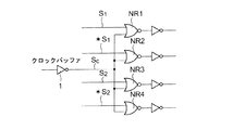
(第11実施形態)
図11は、本発明の第11実施形態に係る半導体集積回路装置の構成を示す回路図である。図11に示す第11実施形態の半導体集積回路装置は、クロックバッファ1から出力されたクロック信号SCを入力する第1ないし第4の2入力NOR回路NR1,NR2,NR3,NR4を備えている。クロック制御信号S1が第1のNOR回路NR1に入力され、クロック制御信号S1の反転信号*S1が第2のNOR回路NR2に入力され、クロック制御信号S2が第3のNOR回路NR3に入力され、クロック制御信号S2の反転信号*S2第4のNOR回路NR4に入力されている。ここで、第1のNOR回路NR1と第3のNOR回路NR3のクロック信号として用いるとすると、それぞれはクロック制御信号S1およびS2に応じてクロックを伝達するかしないかが制御される。
【0052】
ここで、クロックバッファ1から見ると、第1のNOR回路NR1の他方の入力信号S1と第2のNOR回路NR2の他方の入力信号*S1は相補的であるので、クロック制御信号S1の状態に拘わらず一定の負荷を有することになる。これは第3のNOR回路NR3と第4のNOR回路NR4についても同様である。その結果として、クロックバッファ1の負荷は制御信号S1およびS2の状態に拘わらず一定にすることができる。
【0053】
なお、より効果的な構成とするためには、第1および第2のNOR回路NR1およびNR2の回路パラメータを同一とし、第3および第4のNOR回路NR3およびNR4の回路パラメータを同一にすることが望ましい。また、第2のNOR回路NR2の出力負荷を第1のNOR回路NR1の出力負荷と等しくし、第4のNOR回路NR4の出力負荷を第3のNOR回路NR3の出力負荷と等しくすることも効果的である。
【0054】
本第11実施形態においては、2入力NOR回路を用いているが、本発明は他の2入力論理回路においても応用可能である。制御信号S1と制御信号S2が入力される論理回路の種類が異なる場合についても応用可能である。
【0055】
また、本第11実施形態ではクロック制御信号S1およびS2のそれぞれの反転信号*S1および*S2をインバータにより生成しても良く、また、全体の回路構成における何れかの箇所で既に反転信号が生成されている場合には、その信号をそのまま用いるようにすれば、新たに生成する必要はない。
【0056】
この第11実施形態に係る半導体集積回路装置によれば、ゲーティッドクロック信号が他のブロックに供給されるゲーティッドクロック信号を制御する信号の状態により影響を受けないようにすることができる。
【0057】
(第12実施形態)
次に、図12を参照しながらこの発明の第12実施形態に係る半導体集積回路装置について説明する。第12実施形態は本発明をクロックツリーに適用したものである。信号Clockはクロック信号である。Y0は、クロックツリー中の信号、X1,X2,…は制御信号であり、論理ゲートG1,G2,…によって制御されたクロック信号Y1,Y2,…を作成する。このとき、図12に示すように、論理ゲートG1,G1’,G2,G2’,…はそれぞれX1,*X1,X2,*X2…とクロックツリー中のY0を入力として有するような構成とすることにより、Y0からの入力容量C1,C2,…は、信号X1,X2,…の状態によらずに一定とすることができる。また、必要に応じてY1’,Y2’を用いることもできる。
【0058】
このように、本発明の第12実施形態に係る半導体集積回路装置を用いることにより、制御信号と論理ゲートにより制御されたクロック信号の遅延時間のばらつき(スキュー、ジッタ)を抑制することができる。
【0059】
(第13実施形態)
次に、図13を用いて本発明の第13実施形態に係る半導体集積回路装置について説明する。この第13実施形態においては、多入力の論理ゲートまたはそれによって構成されるブロックG1への入力に入力容量無依存化装置8を挿入することによって、ブロックG1への入力容量C1が入力A1〜Amの状態に依存しない構成とすることができる。論理ゲートまたはブロックG1からは出力B1〜Bnが出力されている。なお、論理ゲートまたはブロックG2は入力容量C2が一定であるような論理ゲートあるいはブロックである。このとき、入力容量(C1+C2)が一定となり、入力inから出力outへの遅延時間を入力A1〜Amの状態に依らず一定にすることができる。
【0060】
本発明の第13実施形態に係る半導体集積回路装置を用いることにより、入力容量無依存化装置8に供給される入力について、入力容量無依存化装置を介して入力する1つの論理ゲートやブロックの他の全ての入力の状態に依らず入力容量が一定となる。
【0061】
(第14実施形態)
次に、図14を用いて、本発明の第14の実施形態に係る半導体集積回路装置について説明する。図14に示すように、この第14実施形態は、第13実施形態における入力容量無依存化装置8をインバータ80によって構成したものである。その他の構成は、図13と同一なので重複説明を省略する。
【0062】
本発明の第14実施形態に係る半導体集積回路装置を用いることにより、入力容量無依存化装置につなげた入力について、入力容量無依存化装置を介して入力する論理ゲートやブロックの他の全ての入力の状態に依らず入力容量が一定となる。
【0063】
(第15実施形態)
次に、図15を用いて、本発明の第15実施形態に係る半導体集積回路装置について説明する。
【0064】
図15において、入力inが全ての入力容量無依存化装置8または入力容量の一定な論理ゲートあるいはブロックに入力していれば、入力inの入力容量(Ci)をG1〜GNまでのゲートの入力in以外の全ての入力の状態に依存することなく一定とすることができる。このとき、入力inから入力容量無依存化装置8の出力までの遅延と、入力inから入力容量の一定なゲート、ブロックの出力(out 1〜out k)までの遅延が他の論理ゲートあるいはブロックの入力信号の状態を受けることが無くなる。入力容量の一定な論理ゲートあるいはブロックがない場合もある。
【0065】
本発明の第15実施形態に係る半導体集積回路装置を用いることにより、入力容量無依存化装置につなげた入力について、入力容量無依存化装置を介して入力する全ての論理ゲートやブロックの他の全ての入力の状態に依らず入力容量が一定となる。
【0066】
(第16実施形態)
次に、図16を参照しながら、本発明の第16実施形態に係る半導体集積回路装置について説明する。
【0067】
第16実施形態は、図16に示すように、第15実施形態の入力容量無依存化装置8をインバータ80により実現したものである。このように構成しても、入力inの入力容量を一定とすることができる。その他の構成については、図15と同一なので重複説明を省略する。
【0068】
本発明の第16実施形態に係る半導体集積回路装置を用いることにより、入力容量無依存化装置に接続された入力について、入力容量無依存化装置を介して入力する全ての論理ゲートやブロックの他の全ての入力の状態に依らず入力容量が一定となる。
【0069】
(第17実施形態)
従来のゲーティッドクロック回路では、図22に示すようにクロックバッファ51の出力を直接に2入力NOR回路に入力していたが、本第17実施形態においては、クロック信号が入力されるすべての多入力論理回路について、クロック信号の入力ピンに、バッファ回路6a,6bを入れることとする。このように構成すると、例えば図22の回路は、図17に示されるような回路となる。
【0070】
ルートバッファ51からは2つのバッファ回路6a,6bの容量が見えるだけなので、セレクタ回路57の出力56aおよび56bの状態には無関係になる。その結果として、フリップフロップ55aへのクロック入力のタイミングは出力56bの影響を受けなくなり、フリップフロップ55bへのクロック入力のタイミングは出力56aの影響を受けなくなる。挿入されたバッファ回路6a,6bによりクロック信号が反転する場合にはNOR回路52aおよび52b以降において可能である。本実施形態ではバッファ回路54の後段において、もう1つバッファ回路7をそれぞれ挿入することによってその調節を行なっている。
【0071】
本発明の第17実施形態に係る半導体集積回路装置を用いることにより、あるブロックに属するフリップフロップ55aまたは55bに入力されるクロック信号のタイミングが、他のブロックへ供給されるクロック信号を制御する信号の状態の影響を受けなくなる。
【0072】
(第18実施形態)
次に、図18を参照しながら、本発明の第18実施形態に係る半導体集積回路装置について説明する。
【0073】
この第18実施形態に係る半導体集積回路装置は、図11のNOR回路NR1の詳細な構成を示すものである。図18において、クロックバッファ1から出力されたクロック信号SCは2入力NOR回路(NR1)に入力されている。クロック制御信号S1がNOR回路NR1に入力されている。ここで、NOR回路NR1の出力信号はクロック信号として用いられており、クロック制御信号S1に応じて、クロックを伝達するか、しないかが制御される。
【0074】
クロック信号SCは電源VDDに直接接続されたpMOS1とnMOS1に入力される。クロック制御信号S1はpMOS2とnMOS2に入力される。このように接続することにより、クロックバッファ1から見たNOR回路NR1の入力ピン容量は、クロック制御信号S1がハイであるかローであるかの影響を受け難くなる。図11に示した第2ないし第4のNOR回路NR2〜NR4についても図18と同一の回路構成が適用可能である。ただし、第4のNOR回路NR4は省略することもできる。
【0075】
本発明の第18実施形態に係る半導体集積回路装置を用いることにより、2入力NOR回路のクロック信号入力ピンの入力ピン容量が、制御入力の信号の状態の影響を受け難くすることができる。
【0076】
(第19実施形態)
次に、図19を参照しながら本発明の第19実施形態に係る半導体集積回路装置について詳細に説明する。
【0077】
クロックバッファ1から出力されたクロック信号SCは、2入力NAND回路ND1に入力され、クロック制御信号S1もNAND回路ND1に入力されている。ここで、NAND回路ND1の出力信号はクロック信号として用いられ、クロック制御信号S1に応じて、クロックを伝達するか、しないかが制御される。クロック信号SCはpMOS1と接地GNDに直接接続されたnMOS1に入力される。クロック制御信号S1はpMOS2とnMOS2に入力される。
【0078】
このように接続することにより、クロックバッファ1から見たNAND回路ND1の入力ピン容量は、クロック制御信号SCがハイであるかローであるかの影響を受け難くなる。
【0079】
本発明の第19実施形態に係る半導体集積回路装置を用いることにより、2入力NAND回路のクロック信号入力ピンの入力ピン容量が、制御入力の信号の状態の影響を受け難くすることができる。
【0080】
(第20実施形態)
次に、図20を参照しながら本発明の第20実施形態に係る半導体集積回路装置について説明する。第20実施形態は、第18実施形態および第19実施形態を一般的な多入力論理回路5に応用した例である。ゲーティッドクロック用のクロックツリーを構成することにより、多入力論理回路5を用いてクロックの制御を行なう場合、その多入力論理回路5における必要な論理を形成するために、クロック信号を入力するpMOSおよびnMOSが、図20に破線で示すように、pMOSは直接VDD電源に接続され、nMOSは直接GND電位に接続されるように構成する。
【0081】
本発明の第20実施形態に係る半導体集積回路装置を用いることにより、多入力論理回路のクロック信号入力ピンの入力ピン容量が、制御入力の信号の状態の影響を受け難くすることができる。
【0082】
【発明の効果】
以上、詳細に説明したように、本発明に係る半導体集積回路装置によれば、論理回路が複数の入力を有すると共にこれら複数の入力の信号状態がそれぞれ異なることにより、それぞれの入力ピンの容量に違いが発生する論理回路よりなるものにおいて、前記複数の入力を有する前記論理回路の入力の1つもしくは複数に設けられ、前記複数の入力の状態の如何に拘わらず、この入力が有する入力容量を一定に保つ入力容量等化回路を備えるようにしたので、多入力論理ゲートの入力ピン容量を他の入力信号の状態に関係なく一定にし、集積回路中を伝搬する信号の遅延時間を正確に見積もることができ、複数段または複数並列に設けられた論理素子間の遅延時間を全て一致させることが可能となる。
【図面の簡単な説明】
【図1】本発明の第1実施形態に係る半導体集積回路装置の構成を示すブロック図。
【図2】本発明の第2実施形態に係る半導体集積回路装置の構成を示すブロック図。
【図3】本発明の第3実施形態に係る半導体集積回路装置の構成を示すブロック図。
【図4】本発明の第4実施形態に係る半導体集積回路装置の構成を示すブロック図。
【図5】本発明の第5実施形態に係る半導体集積回路装置の構成を示すブロック図。
【図6】本発明の第6実施形態に係る半導体集積回路装置の構成を示す回路図。
【図7】本発明の第7実施形態に係る半導体集積回路装置の構成を示す回路図。
【図8】本発明の第8実施形態に係る半導体集積回路装置の構成を示す回路図。
【図9】本発明の第9実施形態に係る半導体集積回路装置の構成を示す回路図。
【図10】本発明の第10実施形態に係る半導体集積回路装置の構成を示す回路図。
【図11】本発明の第11実施形態に係る半導体集積回路装置の構成を示す回路図。
【図12】本発明の第12実施形態に係る半導体集積回路装置の構成を示す回路図。
【図13】本発明の第13実施形態に係る半導体集積回路装置の構成を示すブロック図。
【図14】本発明の第14実施形態に係る半導体集積回路装置の構成を示すブロック図。
【図15】本発明の第15実施形態に係る半導体集積回路装置の構成を示すブロック図。
【図16】本発明の第16実施形態に係る半導体集積回路装置の構成を示すブロック図。
【図17】本発明の第17実施形態に係る半導体集積回路装置の構成を示す回路図。
【図18】本発明の第18実施形態に係る半導体集積回路装置の構成を示す回路図。
【図19】本発明の第19実施形態に係る半導体集積回路装置の構成を示す回路図。
【図20】本発明の第20実施形態に係る半導体集積回路装置の構成を示す回路図。
【図21】従来の半導体集積回路装置の構成を示す論理ブロック図。
【図22】従来の半導体集積回路装置の構成を示す回路図。
【符号の説明】
1 クロックバッファ
2,4 入力容量等化装置
6a,6B,7 バッファ回路
5 多入力論理回路
8 入力容量無依存装置
80 インバータ
NR1〜NR8 第1ないし第8のNOR回路
G1〜G2n 論理ゲート/ブロック[0001]
BACKGROUND OF THE INVENTION
The present invention relates to a semiconductor integrated circuit device, and more particularly to a semiconductor integrated circuit device obtained by improving the configuration of logic gates constituting a clock tree.
[0002]
[Prior art]
The delay time of a signal propagating through an integrated circuit is determined by the input capacitance of a logic gate serving as a load, but the input capacitance or delay time in a circuit having a multi-input gate as a load is the state of the other input signal of the multi-input gate. Will be affected. FIG. 21 shows a circuit having a 2-input NAND gate as a load. In FIG. 21, the input capacitance viewed from the input terminal in is (C1 + C2), but the input capacitance C1 of the NAND gate is in the state of the other input A. Affected by.
[0003]
That is, the apparent capacitance C1 differs depending on whether the input A is high or low. As a result, the delay time of the signal transmitted from the input terminal “in” to the output terminal “out” changes. Conventionally, in such a case, the timing design is performed assuming the state of the input A that maximizes the delay time of the signal transmitted from the input terminal in to the output terminal out. In this case, there is a problem that the margin becomes larger by extraly estimating the delay time. Further, it may be necessary to separately perform a timing check assuming the state of the input A where the delay time is minimized.
[0004]
In particular, in a clock tree that distributes a clock signal to an entire LSI (Large Scale Integrated-circuit), it is necessary to perform timing design accurately. In recent years, in order to reduce the power consumption of an LSI, a gated clock method is used in which the supply of a clock signal is partially stopped as necessary, as in the technique disclosed in Japanese Patent Laid-Open No. 10-308450. It is getting to be. FIG. 22 shows a configuration example of a gated clock circuit which is the prior art in FIG. 5 of the above publication. In this circuit, a clock signal is inputted as
[0005]
Here, there is generally no correlation between the operations of the
[0006]
In an LSI, it is common to design so that all clock signals of the flip-
[0007]
[Problems to be solved by the invention]
Thus, it is impossible to design a timing that can reduce the clock skew in all states. As apparent from the technical contents disclosed in FIG. 1 and FIG. 3 cited as an embodiment in the above-mentioned Japanese Patent Application Laid-Open No. 10-308450, this timing design problem has not been solved.
[0008]
The present invention makes it possible to accurately estimate the delay time of a signal propagating in an integrated circuit by making the input pin capacitance of a multi-input logic gate constant regardless of the state of other input signals. An object of the present invention is to provide a semiconductor integrated circuit device capable of designing a circuit.
[0009]
[Means for Solving the Problems]
In order to achieve the above object, a semiconductor integrated circuit device according to a first basic configuration of the present invention includes:One or more first logic circuits that operate according to a first input signal, an input capacitance equalization circuit to which the first input signal is input, one or more second input signals, the input capacitance, and the like One or a plurality of second logic circuits to which the output signal output from the equalization circuit is input, and the input capacitance equalization circuit does not depend on the state of the second input signal. And an input capacitance independence circuit that equalizes the input capacitance of the input signal, and the first logic circuit has a constant input capacitance for performing a predetermined logic operation based on the first input signal. The second logic circuit includes a plurality of logic gate blocks to which the plurality of second input signals and the output of the input capacitance independent circuit are supplied.It is characterized by providing.
[0010]
The firstIntegrated circuit device according to the basic configuration ofThe input capacitance independent circuit may be an inverter.
[0011]
The firstIntegrated circuit device according to the basic configuration ofThe first and second logic circuits each include a two-input one-output logic operation element having the same circuit configuration for performing a predetermined logic operation, and a selection circuit is provided at one input of the logic operation element. The selection signal may be supplied from the other, and the clock signal output from the input capacitance independent circuit may be supplied to the other input of the logic operation element.
[0012]
As described in the paragraph aboveIn a semiconductor integrated circuit device,The input capacitance independent circuit may include a clock buffer that supplies a clock signal to a logic operation element that functions as the first and second logic circuits.
[0016]
First of the present invention2In the semiconductor integrated circuit device including a multi-input logic circuit to which a clock signal and a control signal are input, the clock signal as one input of the multi-input logic circuit is A first MOS transistor directly connected to the power supply potential of the multi-input logic circuit;groundThe second MOS transistor directly connected to the potential is supplied to both gate terminals.
[0017]
DETAILED DESCRIPTION OF THE INVENTION
DESCRIPTION OF EMBODIMENTS Hereinafter, preferred embodiments of a semiconductor integrated circuit device according to the present invention will be described in detail with reference to the accompanying drawings. The semiconductor integrated circuit device according to the first to twentieth embodiments will be described with reference to FIGS. According to a first aspect of the present invention, the logic circuit includes a plurality of inputs, and each of the plurality of inputs has different signal states so that a difference occurs in the capacitance of each input pin. An input capacitance equalization circuit provided at one or more of the inputs of the logic circuit having a plurality of inputs, and keeping the input capacitance of the inputs constant regardless of the state of the plurality of inputs; It is a feature. Therefore, the specific circuit of the logic circuit by the multistage logic element can be any of a clock tree circuit, a logic gate or a logic block. Hereinafter, each embodiment will be described in detail.
[0018]
(First embodiment)
A semiconductor integrated circuit device according to a first embodiment of the present invention will be described with reference to FIG. When there are inputs IN1 and IN2 in a block G1 constituted by a two-input logic gate or a logic gate, the IN1 terminal of the block G1 to which the input signal X is input and the input capacitance are independent of the state of the input signal Y. The
[0019]
As a result, the input capacitance viewed from the input signal X can be made constant. In addition to the input X, the input of the input
[0020]
(Second Embodiment)
Next, a semiconductor integrated circuit device according to a second embodiment of the present invention will be described with reference to FIG. In the second embodiment, the input
[0021]
The block G1 has an input terminal IN1 to which the signal X is input, an input terminal IN2 to which the signal Y is input, and an output terminal OUT to which the signal Z is output, and the block G1 ′ has an input to which the signal X is input. It has a terminal IN3 and an input terminal IN4 to which an inverted signal * Y of the signal Y is input. Reference numerals C1 and C2 denote input capacitances to IN1 of block G1 and IN3 of block G1 '. It is more effective that the circuit parameter of the block G1 'as the equalization circuit is equal to the circuit parameter of the block G1. In this specification, “*” is used as an inversion sign.
[0022]
By using the semiconductor integrated circuit device according to the second embodiment of the present invention, the input capacitance of one input to the two-input gate can be prevented from being affected by the state of the other input signal.
[0023]
(Third embodiment)
Next, a semiconductor integrated circuit device according to a third embodiment of the present invention will be described with reference to FIG. In a logic block G1 configured by a logic gate having (m + n) input terminals IN1 to INm + n to which (m + n) signals X1 to Xm and Y1 to Yn are respectively input, the input terminals IN1 to INm The input capacitance equalizing
[0024]
In the third embodiment, there may be a plurality of output signals of the block G1 such as Z1 to Zk. Further, the input of the
[0025]
By using the semiconductor integrated circuit device according to the third embodiment of the present invention, the input capacitance of at least one input to the multi-input gate is not affected by the state of some of the other input signals. Can be.
[0026]
(Fourth embodiment)
Next, a semiconductor integrated circuit device according to a fourth embodiment of the present invention will be described with reference to FIG. In the circuit device of the fourth embodiment, the input equalization circuit in the circuit device of the third embodiment is a logic gate equivalent to the logic gate G1 or equivalent blocks G2 to G2 constituted by logic gates.nIt is constituted by. In this case, 2 n logic gates or blocks are required.
[0027]
By using the semiconductor integrated circuit device according to the fourth embodiment of the present invention, the input capacitance of at least one input input to the multi-input gate is not affected by the state of some of the multiple input signals. Can be.
[0028]
(Fifth embodiment)
Next, a semiconductor integrated circuit device according to a fifth embodiment of the present invention will be described with reference to FIG. The circuit device according to the fifth embodiment is a configuration example in the case where the inputs X1 to Xm do not exist in the circuit device according to the fourth embodiment. At this time, there are n input signals Y1 to Yn, and the logic gate or logic block G1 has n inputs.
[0029]
As in the fourth embodiment, the input capacitance equalization circuit is equivalent to the logic gate G1 or equivalent blocks G2 to G2 constituted by the logic gates.nConsists of.
[0030]
At this time, the input capacitance viewed from the n input signals Y1 to Yn is constant regardless of the states of all other input signals. At this time, only the inverted signal of Y1 to Yn is input G2.nCan be omitted.
[0031]
By using the semiconductor integrated circuit device according to the fifth embodiment of the present invention, the input capacitance seen from all the input signals input to the multi-input gate is not affected by the state of all other input signals. be able to.
[0032]
(Sixth embodiment)
Next, a semiconductor circuit device according to a sixth embodiment of the present invention will be described with reference to FIG. The sixth embodiment is for making one input pin capacitance of a two-input NOR circuit constant without depending on the state of the other input signal. The circuit is composed of a first two-input NOR circuit NR1 to which signals A and B are inputted, and a second two-input NOR circuit NR2 to which an inverted signal * A of the signal A and a signal B are inputted. The signal * A is appropriately generated using an inverter circuit or the like. Here, the other input signal of the first NOR circuit NR1 and the other input signal of the second NOR circuit NR2 are complementary. In other words, when the potential of the signal A is high, the potential of the signal * A is When the signal A is in the low state and the signal A is in the low state, the signal * A is in the high state. That is, when viewed from the signal B, regardless of the state of the signal A, there is one 2-input NOR circuit whose other input is high and one 2-input NOR circuit whose other input is low. Regardless of the state, it becomes constant.
[0033]
The closer the circuit parameters of the first and second NOR circuits NR1 and NR2 are, the more effective. Further, the load on the output of the second NOR circuit NR2 is more effective as the load is closer to the output load of the first NOR circuit NR1. Although the sixth embodiment has been described using a two-input NOR circuit, the present invention can also be applied to other two-input logic circuits.
[0034]
According to the semiconductor integrated circuit device according to the second embodiment configured as described above, the input capacitance of one input pin of the two-input logic circuit can be prevented from being affected by the state of the other input signal. .
[0035]
(Seventh embodiment)
Next, a semiconductor integrated circuit device according to a seventh embodiment of the present invention will be described with reference to FIG. In the seventh embodiment, the input pin capacities of the two input pins of the two-input NOR circuit are made constant regardless of the state of the input signal of the other input pin. The semiconductor integrated circuit device according to the seventh embodiment includes first to fourth two-input NOR circuits NR1, NR2, NR3 and NR4. The first NOR circuit NR1 receives the signals A and B, the second NOR circuit NR2 receives the inverted signal * A and the signal B of the signal A, and the third NOR circuit NR3 receives the signals A and B. The inverted signal * B of the signal B is input, and the inverted signal * A of the signal A and the inverted signal * B of the signal B are input to the fourth NOR circuit NR4. The inversion signals * A and * B can be generated using an inverter or the like as necessary.
[0036]
Here, when viewed from the input A, the loads are the first and third NOR circuits NR1 and NR3. The other inputs of the first and third NOR circuits NR1 and NR3 are the signal B and the signal * B, respectively, and the pin capacity of the input A is constant regardless of the state of the signal B. Apart from this, if there is an inverter that generates the signal * A, its capacity is added. Next, when viewed from the input B, the loads are the first and second NOR circuits NR1 and NR2. The other inputs of the first and second NOR circuits NR1 and NR2 are the signal A and the signal * A, and the input pin capacitance of the input B is constant regardless of the state of the signal A. Apart from this, if there is an inverter that generates the signal * B, its capacity is added.
[0037]
Since the output of the 2-input NOR circuit was originally required, the output of the first NOR circuit NR1 is connected to the next stage circuit. Here, it is more effective that the output loads of the second to fourth NOR circuits NR2, NR3, and NR4 are the same as those of the first NOR circuit NR1. It is also effective to make the circuit parameters of the first to fourth NOR circuits NR1 to NR4 as equal as possible. The fourth NOR circuit NR4 can be omitted. Although the seventh embodiment has been described using a two-input NOR circuit, the present invention can also be applied to other two-input logic circuits.
[0038]
By using the semiconductor integrated circuit device according to the seventh embodiment, it is possible to prevent the input capacitance of any one input pin of the two-input logic circuit from being affected by the state of the other input signal.
[0039]
(Eighth embodiment)
Next, a semiconductor integrated circuit device according to an eighth embodiment of the present invention will be described with reference to FIG. The eighth embodiment is an example in which the circuit device of the seventh embodiment is applied to a three-input logic circuit. The semiconductor integrated circuit device according to the eighth embodiment includes first to fourth three-input NOR circuits NR1 to NR4. Signal A, signal B, and signal C are input to the first NOR circuit NR1. Inverted signal * A, signal B, and signal C of signal A are input to the second NOR circuit NR2. The third NOR circuit NR3 receives the signal A, the inverted signal * B of the signal B, and the signal C. The fourth NOR circuit NR4 receives the inverted signal * A of the signal A, the inverted signal * B of the signal B, and the signal C. From the viewpoint of the signal C, a 3-input NOR circuit in which the first input is high and the second input is high regardless of the states of the signals A and B, and the first input is high and the second input is low 3. The load is an input NOR circuit, a three-input NOR circuit in which the first input is low and the second input is high, and a three-input NOR circuit in which the first input is low and the second input is low. As a result, the input pin capacitance of input C is always kept constant.
[0040]
Since the output of the 3-input NOR circuit was originally required, the output of the first NOR circuit NR1 is connected to the next stage circuit. Here, it is more effective that the output loads of the second to fourth NOR circuits NR2, NR3, and NR4 are the same as those of the first NOR circuit NR1. It is also effective to make the circuit parameters of the first to fourth NOR circuits NR1 to NR4 as equal as possible. Although the eighth embodiment has been described using a three-input NOR circuit, the present invention can also be applied to other three-input logic circuits.
[0041]
By using the semiconductor integrated circuit device according to the eighth embodiment, it is possible to prevent the input capacitance of any one input pin of the three-input logic circuit from being affected by the state of the other input signal.
[0042]
(Ninth embodiment)
Next, a semiconductor integrated circuit device according to a ninth embodiment of the present invention will be described with reference to FIG. The circuit device according to the ninth embodiment is an example in which the circuit device according to the seventh embodiment is applied to a three-input logic circuit. The ninth embodiment includes first to eighth three-input NOR circuits NR1 to NR8. Signal A, signal B, and signal C are input to the first NOR circuit NR1. Inverted signal * A, signal B, and signal C of signal A are input to the second NOR circuit NR2. The third NOR circuit NR3 receives the signal A, the inverted signal * B of the signal B, and the signal C. The fourth NOR circuit NR4 receives the inverted signal * A of the signal A, the inverted signal * B of the signal B, and the signal C.
[0043]
The fifth NOR circuit NR5 receives the signal A, the signal B, and the inverted signal * C of the signal C. The sixth NOR circuit NR6 receives the inverted signal * A of the signal A, the signal B, and the inverted signal * C of the signal C. The seventh NOR circuit NR7 receives the signal A, the inverted signal * B of the signal B, and the inverted signal * C of the signal C. The eighth NOR circuit NR8 receives an inverted signal * A of the signal A, an inverted signal * B of the signal B, and an inverted signal * C of the signal C.
[0044]
From the viewpoint of the signal C, a 3-input NOR circuit in which the first input is high and the second input is high regardless of the states of the signals A and B, and the first input is high and the second input is low 3. The load is an input NOR circuit, a three-input NOR circuit in which the first input is low and the second input is high, and a three-input NOR circuit in which the first input is low and the second input is low. When the inverted signal * C of the signal C is generated by an inverter, an inverter capacity is added to them. As a result, the input pin capacitance of input C is always kept constant. The same applies to input A and input B.
[0045]
Since the output of the 3-input NOR circuit was originally required, the output of the first NOR circuit NR1 is connected to the next stage circuit. Here, it is more effective that the output loads of the second to eighth NOR circuits NR2 to NR8 are the same as those of the first NOR circuit NR1. It is also effective to make the circuit parameters of the first to eighth NOR circuits NR1 to NR8 as equal as possible. Although the ninth embodiment has been described using a three-input NOR circuit, the present invention can also be applied to other three-input logic circuits. Further, the eighth NOR circuit NR8 can be omitted.
[0046]
By using the semiconductor integrated circuit device according to the ninth embodiment of the present invention, it is possible to prevent the input capacitances of all the input pins of the three-input logic circuit from being affected by the state of other input signals. .
[0047]
(10th Embodiment)
Next, a semiconductor integrated circuit device according to a tenth embodiment of the present invention will be described with reference to FIG. The circuit device according to the tenth embodiment is an example in which the input pin capacitance is equalized for two input signals out of three input signals. The tenth embodiment includes first to sixth three-input NOR circuits NR1 to NR6. Signal A, signal B, and signal C are input to the first NOR circuit NR1. Inverted signal * A, signal B, and signal C of signal A are input to the second NOR circuit NR2. The third NOR circuit NR3 receives the signal A, the inverted signal * B of the signal B, and the signal C. The fourth NOR circuit NR4 receives the inverted signal * A of the signal A, the inverted signal * B of the signal B, and the signal C. The fifth NOR circuit NR5 receives the signal A, the signal B, and the inverted signal * C of the signal C. The sixth NOR circuit NR6 receives the inverted signal * A of the signal A, the signal B, and the inverted signal * C of the signal C.
[0048]
From the viewpoint of the signal C, a 3-input NOR circuit in which the first input is high and the second input is high, regardless of the states of the signals A and B, the first input is high and the second input is low. The load is a 3-input NOR circuit, a 3-input NOR circuit in which the first input is low and the second input is high, and a 3-input NOR circuit in which the first input is low and the second input is low. When the inverted signal * C of the signal C is generated by an inverter, an inverter capacity is added to them. As a result, the input pin capacitance of input C is always kept constant. The same applies to input B. However, since only three NOR circuits are connected to the signal A, the input capacitance viewed from the signal A varies depending on the states of the signals B and C.
[0049]
Since the output of the 3-input NOR circuit was originally required, the output of the first NOR circuit NR1 is connected to the next stage circuit. Here, it is more effective that the output loads of the second to sixth NOR circuits NR2 to NR6 are the same as those of the first NOR circuit NR1. It is also effective to make the circuit parameters of the first to sixth NOR circuits NR1 to NR6 as equal as possible. In the tenth embodiment, the description has been given using the three-input NOR circuit, but the present invention can also be applied to other three-input logic circuits.
[0050]
By using the semiconductor integrated circuit device according to the tenth embodiment of the present invention, it is possible to prevent the input capacitances of all the input pins of the three-input logic circuit from being affected by the state of other input signals. .
[0051]
(Eleventh embodiment)
FIG. 11 is a circuit diagram showing a configuration of a semiconductor integrated circuit device according to the eleventh embodiment of the present invention. The semiconductor integrated circuit device according to the eleventh embodiment shown in FIG. 11 includes first to fourth 2-input NOR circuits NR1, NR2, NR3, and NR4 that receive the clock signal SC output from the
[0052]
Here, when viewed from the
[0053]
In order to obtain a more effective configuration, the circuit parameters of the first and second NOR circuits NR1 and NR2 are made the same, and the circuit parameters of the third and fourth NOR circuits NR3 and NR4 are made the same. Is desirable. It is also effective to make the output load of the second NOR circuit NR2 equal to the output load of the first NOR circuit NR1, and make the output load of the fourth NOR circuit NR4 equal to the output load of the third NOR circuit NR3. Is.
[0054]
In the eleventh embodiment, a two-input NOR circuit is used, but the present invention can also be applied to other two-input logic circuits. The present invention can also be applied to a case where the types of logic circuits to which the control signal S1 and the control signal S2 are input are different.
[0055]
In the eleventh embodiment, the inverted signals * S1 and * S2 of the clock control signals S1 and S2 may be generated by an inverter, and an inverted signal is already generated at any point in the entire circuit configuration. In such a case, if the signal is used as it is, it is not necessary to newly generate it.
[0056]
According to the semiconductor integrated circuit device of the eleventh embodiment, the gated clock signal can be prevented from being affected by the state of the signal that controls the gated clock signal supplied to other blocks.
[0057]
(Twelfth embodiment)
Next, a semiconductor integrated circuit device according to a twelfth embodiment of the present invention will be described with reference to FIG. In the twelfth embodiment, the present invention is applied to a clock tree. The signal Clock is a clock signal. Y0 is a signal in the clock tree, X1, X2,... Are control signals, which generate clock signals Y1, Y2,. At this time, as shown in FIG. 12, the logic gates G1, G1 ′, G2, G2 ′,... Are configured to have X1, * X1, X2, * X2. Thus, the input capacitors C1, C2,... From Y0 can be made constant regardless of the state of the signals X1, X2,. Further, Y1 'and Y2' can be used as necessary.
[0058]
As described above, by using the semiconductor integrated circuit device according to the twelfth embodiment of the present invention, it is possible to suppress variation (skew, jitter) in the delay time of the control signal and the clock signal controlled by the logic gate.
[0059]
(13th Embodiment)
Next, a semiconductor integrated circuit device according to a thirteenth embodiment of the present invention is described with reference to FIG. In the thirteenth embodiment, an input
[0060]
By using the semiconductor integrated circuit device according to the thirteenth embodiment of the present invention, the input supplied to the input
[0061]
(14th Embodiment)
Next, a semiconductor integrated circuit device according to a fourteenth embodiment of the present invention will be described with reference to FIG. As shown in FIG. 14, in the fourteenth embodiment, the input capacity
[0062]
By using the semiconductor integrated circuit device according to the fourteenth embodiment of the present invention, all the other logic gates and blocks that are input via the input capacitance independent device are input to the input capacitance independent device. The input capacity is constant regardless of the input state.
[0063]
(Fifteenth embodiment)
Next, a semiconductor integrated circuit device according to a fifteenth embodiment of the present invention will be described with reference to FIG.
[0064]
In FIG. 15, if input in is input to all input
[0065]
By using the semiconductor integrated circuit device according to the fifteenth embodiment of the present invention, the input connected to the input capacitance independence device, all the logic gates and other blocks input through the input capacitance independence device The input capacity is constant regardless of the state of all inputs.
[0066]
(Sixteenth embodiment)
Next, a semiconductor integrated circuit device according to a sixteenth embodiment of the present invention will be described with reference to FIG.
[0067]
In the sixteenth embodiment, as shown in FIG. 16, the input capacity
[0068]
By using the semiconductor integrated circuit device according to the sixteenth embodiment of the present invention, all the logic gates and blocks that are input via the input capacitance independence device for the input connected to the input capacitance independence device The input capacitance is constant regardless of the state of all inputs.
[0069]
(17th Embodiment)
In the conventional gated clock circuit, the output of the
[0070]
Since only the capacity of the two
[0071]
By using the semiconductor integrated circuit device according to the seventeenth embodiment of the present invention, the timing of the clock signal input to the flip-
[0072]
(Eighteenth embodiment)
Next, a semiconductor integrated circuit device according to an eighteenth embodiment of the present invention will be described with reference to FIG.
[0073]
The semiconductor integrated circuit device according to the eighteenth embodiment shows a detailed configuration of the NOR circuit NR1 of FIG. In FIG. 18, the clock signal SC output from the
[0074]
The clock signal SC is input to pMOS1 and nMOS1 directly connected to the power supply VDD. The clock control signal S1 is input to the pMOS2 and the nMOS2. By connecting in this way, the input pin capacity of the NOR circuit NR1 viewed from the
[0075]
By using the semiconductor integrated circuit device according to the eighteenth embodiment of the present invention, the input pin capacitance of the clock signal input pin of the two-input NOR circuit can be made less susceptible to the influence of the state of the control input signal.
[0076]
(Nineteenth embodiment)
Next, a semiconductor integrated circuit device according to a nineteenth embodiment of the present invention will be described in detail with reference to FIG.
[0077]
The clock signal SC output from the
[0078]
By connecting in this way, the input pin capacity of the NAND circuit ND1 viewed from the
[0079]
By using the semiconductor integrated circuit device according to the nineteenth embodiment of the present invention, the input pin capacitance of the clock signal input pin of the two-input NAND circuit can be made less susceptible to the influence of the state of the control input signal.
[0080]
(20th embodiment)
Next, a semiconductor integrated circuit device according to a twentieth embodiment of the present invention will be described with reference to FIG. The twentieth embodiment is an example in which the eighteenth embodiment and the nineteenth embodiment are applied to a general
[0081]
By using the semiconductor integrated circuit device according to the twentieth embodiment of the present invention, the input pin capacitance of the clock signal input pin of the multi-input logic circuit can be made less susceptible to the influence of the state of the control input signal.
[0082]
【The invention's effect】
As described above in detail, according to the semiconductor integrated circuit device of the present invention, the logic circuit has a plurality of inputs and the signal states of the plurality of inputs are different from each other. In the case of a logic circuit in which a difference occurs, it is provided at one or more of the inputs of the logic circuit having the plurality of inputs, and the input capacitance of the inputs is determined regardless of the state of the plurality of inputs. Since the input capacitance equalization circuit that keeps constant is provided, the input pin capacitance of the multi-input logic gate is made constant regardless of the state of other input signals, and the delay time of the signal propagating in the integrated circuit is accurately estimated Therefore, it is possible to make all delay times between the logic elements provided in a plurality of stages or a plurality of stages in parallel.
[Brief description of the drawings]
FIG. 1 is a block diagram showing a configuration of a semiconductor integrated circuit device according to a first embodiment of the present invention.
FIG. 2 is a block diagram showing a configuration of a semiconductor integrated circuit device according to a second embodiment of the present invention.
FIG. 3 is a block diagram showing a configuration of a semiconductor integrated circuit device according to a third embodiment of the present invention.
FIG. 4 is a block diagram showing a configuration of a semiconductor integrated circuit device according to a fourth embodiment of the present invention.
FIG. 5 is a block diagram showing a configuration of a semiconductor integrated circuit device according to a fifth embodiment of the present invention.
FIG. 6 is a circuit diagram showing a configuration of a semiconductor integrated circuit device according to a sixth embodiment of the present invention.
FIG. 7 is a circuit diagram showing a configuration of a semiconductor integrated circuit device according to a seventh embodiment of the present invention.
FIG. 8 is a circuit diagram showing a configuration of a semiconductor integrated circuit device according to an eighth embodiment of the present invention.
FIG. 9 is a circuit diagram showing a configuration of a semiconductor integrated circuit device according to a ninth embodiment of the present invention.
FIG. 10 is a circuit diagram showing a configuration of a semiconductor integrated circuit device according to a tenth embodiment of the present invention.
FIG. 11 is a circuit diagram showing a configuration of a semiconductor integrated circuit device according to an eleventh embodiment of the present invention.
FIG. 12 is a circuit diagram showing a configuration of a semiconductor integrated circuit device according to a twelfth embodiment of the present invention.
FIG. 13 is a block diagram showing a configuration of a semiconductor integrated circuit device according to a thirteenth embodiment of the present invention.
FIG. 14 is a block diagram showing a configuration of a semiconductor integrated circuit device according to a fourteenth embodiment of the present invention.
FIG. 15 is a block diagram showing a configuration of a semiconductor integrated circuit device according to a fifteenth embodiment of the present invention.
FIG. 16 is a block diagram showing a configuration of a semiconductor integrated circuit device according to a sixteenth embodiment of the present invention.
FIG. 17 is a circuit diagram showing a configuration of a semiconductor integrated circuit device according to a seventeenth embodiment of the present invention.
FIG. 18 is a circuit diagram showing a configuration of a semiconductor integrated circuit device according to an eighteenth embodiment of the present invention.
FIG. 19 is a circuit diagram showing a configuration of a semiconductor integrated circuit device according to a nineteenth embodiment of the present invention.
FIG. 20 is a circuit diagram showing a configuration of a semiconductor integrated circuit device according to a twentieth embodiment of the present invention.
FIG. 21 is a logic block diagram showing a configuration of a conventional semiconductor integrated circuit device.
FIG. 22 is a circuit diagram showing a configuration of a conventional semiconductor integrated circuit device.
[Explanation of symbols]
1 clock buffer
2,4 input capacity equalizer
6a, 6B, 7 Buffer circuit
5 Multi-input logic circuit
8 Input capacity independent device
80 inverter
NR1 to NR8 first to eighth NOR circuits
G1 to G2n Logic gate / block
Claims (5)
前記第1の論理回路は、前記第1の入力信号に基づいて所定の論理動作を行なうために一定の入力容量を有するゲートブロックを備え、前記第2の論理回路は、前記複数の第2の入力信号および前記入力容量無依存化回路の出力が供給される複数の論理ゲートブロックを備えることを特徴する半導体集積回路装置。 One or more first logic circuits that operate according to a first input signal, an input capacitance equalization circuit to which the first input signal is input, one or more second input signals, the input capacitance, and the like One or a plurality of second logic circuits to which the output signal output from the equalization circuit is input, and the input capacitance equalization circuit does not depend on the state of the second input signal. An input capacitance independent circuit that equalizes the input capacitance of the input signal of
The first logic circuit includes a gate block having a fixed input capacitance for performing a predetermined logic operation based on the first input signal, and the second logic circuit includes the plurality of second logic circuits. A semiconductor integrated circuit device comprising a plurality of logic gate blocks to which an input signal and an output of the input capacitance independent circuit are supplied .
前記多入力論理回路の1つの入力としての前記クロック信号は、前記多入力論理回路の電源電位に直接接続される第1のMOSトランジスタと、接地電位に直接接続される第2のMOSトランジスタと、の双方のゲート端子に供給されることを特徴とする半導体集積回路装置。 In a semiconductor integrated circuit device including a multi-input logic circuit to which a clock signal and a control signal are input,
The clock signal as one input of the multi-input logic circuit includes a first MOS transistor directly connected to a power supply potential of the multi-input logic circuit, a second MOS transistor directly connected to a ground potential, be supplied to both the gate terminal semiconductors integrated circuit device it said the.
Priority Applications (4)
| Application Number | Priority Date | Filing Date | Title |
|---|---|---|---|
| JP2000044307A JP3901906B2 (en) | 2000-02-22 | 2000-02-22 | Semiconductor integrated circuit device |
| TW090103704A TW483116B (en) | 2000-02-22 | 2001-02-19 | Semiconductor integrated circuit device |
| US09/788,413 US6476639B2 (en) | 2000-02-22 | 2001-02-21 | Semiconductor integrated circuit device capable of producing output thereof without being influenced by other input |
| KR10-2001-0008964A KR100392038B1 (en) | 2000-02-22 | 2001-02-22 | Semiconductor integrated circuit device |
Applications Claiming Priority (1)
| Application Number | Priority Date | Filing Date | Title |
|---|---|---|---|
| JP2000044307A JP3901906B2 (en) | 2000-02-22 | 2000-02-22 | Semiconductor integrated circuit device |
Publications (3)
| Publication Number | Publication Date |
|---|---|
| JP2001237691A JP2001237691A (en) | 2001-08-31 |
| JP2001237691A5 JP2001237691A5 (en) | 2005-06-09 |
| JP3901906B2 true JP3901906B2 (en) | 2007-04-04 |
Family
ID=18567085
Family Applications (1)
| Application Number | Title | Priority Date | Filing Date |
|---|---|---|---|
| JP2000044307A Expired - Fee Related JP3901906B2 (en) | 2000-02-22 | 2000-02-22 | Semiconductor integrated circuit device |
Country Status (4)
| Country | Link |
|---|---|
| US (1) | US6476639B2 (en) |
| JP (1) | JP3901906B2 (en) |
| KR (1) | KR100392038B1 (en) |
| TW (1) | TW483116B (en) |
Families Citing this family (4)
| Publication number | Priority date | Publication date | Assignee | Title |
|---|---|---|---|---|
| US7006962B1 (en) * | 2001-11-29 | 2006-02-28 | Lsi Logic Corporation | Distributed delay prediction of multi-million gate deep sub-micron ASIC designs |
| US9638743B2 (en) * | 2014-01-16 | 2017-05-02 | Qualcomm Incorporated | State-dependent capacitance estimation |
| EP3542216A4 (en) | 2016-11-18 | 2020-10-07 | Magic Leap, Inc. | Multilayer liquid crystal diffractive gratings for redirecting light of wide incident angle ranges |
| CN115097625A (en) | 2017-03-21 | 2022-09-23 | 奇跃公司 | Optical device, head-mounted display, imaging system and method of imaging an object |
Family Cites Families (4)
| Publication number | Priority date | Publication date | Assignee | Title |
|---|---|---|---|---|
| JPS6342090A (en) * | 1986-08-07 | 1988-02-23 | Fujitsu Ltd | Signal change detection circuit |
| US5391941A (en) * | 1993-09-23 | 1995-02-21 | Cypress Semiconductor Corporation | Decoder circuitry with balanced propagation delay and minimized input capacitance |
| US5793551A (en) * | 1995-06-07 | 1998-08-11 | Vtc Inc. | Amplifier having a differential input capacitance cancellation circuit |
| JP3178371B2 (en) | 1997-05-06 | 2001-06-18 | 日本電気株式会社 | Design method of semiconductor integrated circuit |
-
2000
- 2000-02-22 JP JP2000044307A patent/JP3901906B2/en not_active Expired - Fee Related
-
2001
- 2001-02-19 TW TW090103704A patent/TW483116B/en not_active IP Right Cessation
- 2001-02-21 US US09/788,413 patent/US6476639B2/en not_active Expired - Fee Related
- 2001-02-22 KR KR10-2001-0008964A patent/KR100392038B1/en not_active IP Right Cessation
Also Published As
| Publication number | Publication date |
|---|---|
| KR20010083242A (en) | 2001-08-31 |
| US6476639B2 (en) | 2002-11-05 |
| US20010015658A1 (en) | 2001-08-23 |
| TW483116B (en) | 2002-04-11 |
| JP2001237691A (en) | 2001-08-31 |
| KR100392038B1 (en) | 2003-07-23 |
Similar Documents
| Publication | Publication Date | Title |
|---|---|---|
| US6879200B2 (en) | Delay circuit, semiconductor integrated circuit device containing a delay circuit and delay method | |
| US20050270066A1 (en) | Level shifter and buffer circuit | |
| US20010048333A1 (en) | Buffer circuit block and design method of semiconductor integrated circuit by using the same | |
| US5703513A (en) | Master-slave bistable latch with clock input control | |
| JP4412893B2 (en) | Semiconductor integrated circuit and manufacturing method thereof | |
| US7157930B2 (en) | Scan flip flop, semiconductor device, and production method of semiconductor device | |
| US7289375B2 (en) | Data holding circuit | |
| JP4035923B2 (en) | Latch circuit | |
| US6861877B2 (en) | Circuit to independently adjust rise and fall edge timing of a signal | |
| JPH04219012A (en) | Semiconductor integrated circuit | |
| JP3901906B2 (en) | Semiconductor integrated circuit device | |
| JP3582967B2 (en) | Latch circuit and flip-flop circuit with clock signal level conversion function | |
| US6879186B2 (en) | Pseudo-dynamic latch deracer | |
| US6489811B2 (en) | Logic gate with symmetrical propagation delay from any input to any output and a controlled output pulse width | |
| JP2000059204A (en) | Dynamic logic circuit and semiconductor integrated circuit device | |
| US20060290386A1 (en) | NAND gate, a NOR gate, and output buffer and method thereof | |
| KR19980083817A (en) | Semiconductor Memory Device with Separate Clock Input Buffer | |
| KR20000074505A (en) | Logic interface circuit and semiconductor memory device using this circuit | |
| KR100429887B1 (en) | Data latch circuit for minimizing loading difference between fetch signal and multiple data in semiconductor device | |
| US9569570B2 (en) | Configurable delay cell | |
| US11277133B1 (en) | Level shifter with isolation logic | |
| US6759877B1 (en) | Dynamic circuitry with on-chip temperature-controlled keeper device | |
| US11074945B1 (en) | Tri-state buffering techniques | |
| JPH09232919A (en) | Latch circuit and flip-flop circuit | |
| JPH04145720A (en) | Logic circuit |
Legal Events
| Date | Code | Title | Description |
|---|---|---|---|
| A521 | Written amendment |
Free format text: JAPANESE INTERMEDIATE CODE: A523 Effective date: 20040903 |
|
| A621 | Written request for application examination |
Free format text: JAPANESE INTERMEDIATE CODE: A621 Effective date: 20040903 |
|
| A977 | Report on retrieval |
Free format text: JAPANESE INTERMEDIATE CODE: A971007 Effective date: 20060217 |
|
| A131 | Notification of reasons for refusal |
Free format text: JAPANESE INTERMEDIATE CODE: A131 Effective date: 20060228 |
|
| A521 | Written amendment |
Free format text: JAPANESE INTERMEDIATE CODE: A523 Effective date: 20060407 |
|
| A131 | Notification of reasons for refusal |
Free format text: JAPANESE INTERMEDIATE CODE: A131 Effective date: 20061027 |
|
| A521 | Written amendment |
Free format text: JAPANESE INTERMEDIATE CODE: A523 Effective date: 20061201 |
|
| TRDD | Decision of grant or rejection written | ||
| A01 | Written decision to grant a patent or to grant a registration (utility model) |
Free format text: JAPANESE INTERMEDIATE CODE: A01 Effective date: 20061222 |
|
| A61 | First payment of annual fees (during grant procedure) |
Free format text: JAPANESE INTERMEDIATE CODE: A61 Effective date: 20061227 |
|
| FPAY | Renewal fee payment (event date is renewal date of database) |
Free format text: PAYMENT UNTIL: 20110112 Year of fee payment: 4 |
|
| FPAY | Renewal fee payment (event date is renewal date of database) |
Free format text: PAYMENT UNTIL: 20120112 Year of fee payment: 5 |
|
| FPAY | Renewal fee payment (event date is renewal date of database) |
Free format text: PAYMENT UNTIL: 20130112 Year of fee payment: 6 |
|
| LAPS | Cancellation because of no payment of annual fees |