JP3898705B2 - Arithmetic unit - Google Patents
Arithmetic unit Download PDFInfo
- Publication number
- JP3898705B2 JP3898705B2 JP2004107646A JP2004107646A JP3898705B2 JP 3898705 B2 JP3898705 B2 JP 3898705B2 JP 2004107646 A JP2004107646 A JP 2004107646A JP 2004107646 A JP2004107646 A JP 2004107646A JP 3898705 B2 JP3898705 B2 JP 3898705B2
- Authority
- JP
- Japan
- Prior art keywords
- data
- carry
- addition
- adder
- partial product
- Prior art date
- Legal status (The legal status is an assumption and is not a legal conclusion. Google has not performed a legal analysis and makes no representation as to the accuracy of the status listed.)
- Expired - Fee Related
Links
Images








Description
本発明は、整数の演算と2の拡大体(ガロア体)の演算とを実行可能な演算装置に係り、特に、両演算を小さい回路規模で高速に実行し得る演算装置に関する。 The present invention relates to an arithmetic device capable of executing an integer operation and an operation of an extension field of 2 (Galois field), and more particularly to an arithmetic device capable of executing both operations at a high speed with a small circuit scale.
従来、整数の演算と2の拡大体の演算とをいずれも実行可能な演算装置が知られている(例えば、特許文献1参照)。 2. Description of the Related Art Conventionally, there has been known an arithmetic device that can execute both integer arithmetic and arithmetic of an extension field of 2 (see, for example, Patent Document 1).
この演算装置では、例えば整数乗算と拡大体乗算を実現するために、図13に示す如き、乗算結果の一部である部分積を加算するための部分積加算回路と、図14に示す如き、この部分積加算回路を構成する全加算器(FA:Full Adder)とを備えている。 In this arithmetic unit, for example, in order to realize integer multiplication and expansion field multiplication, as shown in FIG. 13, a partial product addition circuit for adding a partial product which is a part of the multiplication result, as shown in FIG. A full adder (FA) constituting the partial product adder circuit.
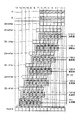
部分積加算回路は、図13に示す場合、7ビットのデータA(=a0,…,a6)と7ビットのデータB(=b0,…,b6)とを乗算したとき、得られる7つの部分積Z0(=A・b0),Z1(=A・b1),…,Z6(=A・b6)を順次加算する。 In the case of the partial product adder circuit shown in FIG. 13, when the 7-bit data A (= a0,..., A6) and the 7-bit data B (= b0,..., B6) are multiplied, The products Z0 (= A · b0), Z1 (= A · b1),..., Z6 (= A · b6) are sequentially added.
この種の部分積加算回路は、制御信号CEによって桁上げ(キャリー)出力Cの有無を切換可能な全加算器FAを備えたことにより、桁上げのある整数の乗算と、桁上げの無い拡大体の乗算とのいずれも実行可能となっている。 This type of partial product addition circuit includes a full adder FA that can switch the presence or absence of a carry output C by a control signal CE, thereby multiplying an integer with a carry and an enlargement without a carry. Both field multiplication and execution are possible.
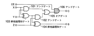
詳しくは、全加算器FAは、アンドゲート101,102,106、排他的論理和ゲート103,104及びオアゲート105を備え、入力信号として、データ入力X,Y,Z及び制御入力CEがあり、出力信号として、桁上げ出力C及び和出力Sがある。これにより、全加算器FAは、データ入力X,Y,Zが排他的論理和ゲート103,104を通過して得られた排他的論理和を、和出力Sとして出力する。また、全加算器FAは、データ入力X,Yがアンドゲート101を通過して得られた論理積と、データ入力X,Yが排他的論理和ゲート103を通過して得られた排他的論理和とデータ入力Zとがアンドゲート102を通過して得られた論理積と、からなる両論理積がオアゲート105を通過して得られた論理和をアンドゲート106を介して桁上げ出力Cとして出力する。
Specifically, the full adder FA includes AND
ここで、アンドゲート106はキャリー出力Cを切換制御する機能を持つ。アンドゲート106は、制御入力CEが‘H’のときにのみ、桁上げ入力(キャリー信号)を出力し、制御入力CEが‘L’のときには、桁上げ入力の値によらずに桁上げ出力‘0’を出力する。 Here, the AND gate 106 has a function of switching and controlling the carry output C. The AND gate 106 outputs a carry input (carry signal) only when the control input CE is “H”. When the control input CE is “L”, the AND gate 106 outputs a carry regardless of the value of the carry input. '0' is output.
例えば整数の演算の際には、制御入力CEを‘H’として桁上げ出力Cを有効にし、部分積Z0,Z1,…,Z6を順次加算していき、最終的に結果Rを得る。ここで、部分積Zi(i=0〜6)は、Aとbi(i=0〜6)の論理積の結果である。すなわち、最初に加算器110−0により、部分積Z0,Z1の和が求められ、次に加算器110−1により、部分積の和(Z0+Z1)と部分積Z2との和が求められる。以下同様にして、最終的に積R=A×Bの結果が得られる。 For example, when calculating an integer, the control input CE is set to 'H', the carry output C is validated, the partial products Z0, Z1,..., Z6 are sequentially added, and the result R is finally obtained. Here, the partial product Zi (i = 0 to 6) is a result of the logical product of A and bi (i = 0 to 6). That is, first, the adder 110-0 obtains the sum of the partial products Z0 and Z1, and then the adder 110-1 obtains the sum of the partial products (Z0 + Z1) and the partial product Z2. In the same manner, the result of the product R = A × B is finally obtained.
一方、拡大体の演算は、整数の演算とは異なり、桁上げが無いので、下位の演算結果が上位の演算結果に影響しない。このため、拡大体の演算は、全加算器FAにて、桁上げ出力Cを無効にし、排他論理和からなる和出力Sのみで実行される。 On the other hand, the arithmetic operation of the extension field is different from the arithmetic operation of the integer, and since there is no carry, the lower operation result does not affect the upper operation result. For this reason, the calculation of the expansion field is executed by the full adder FA with the carry output C invalidated and only the sum output S composed of exclusive OR.
例えば拡大体の乗算の際には、全ての加算器の桁上げ出力を‘0’とするので、乗算結果として、部分積Z0〜Z6の排他論理和の結果である和出力Sが出力される。 For example, in the multiplication of the expansion field, the carry output of all the adders is set to “0”, so that the sum output S that is the result of the exclusive OR of the partial products Z0 to Z6 is output as the multiplication result. .
以上のように整数の演算と拡大体の演算とはそれぞれ実行可能となっている。
また一方、整数乗算のみを実現する演算装置が知られている。この演算装置は、図13に示した部分積加算回路を、図15に示すように、複数の入力を加算して次段に出力するようにツリー状に配置された桁上げ保存加算器(CSA:Carry Save Adder)112−1〜112−5と、最後尾に配置された桁上げ伝搬加算器(CPA:Carry Propagate Adder)113とにより実現する方式である(例えば、非特許文献1参照)。
As described above, the integer operation and the expansion field operation can be executed.
On the other hand, an arithmetic device that realizes only integer multiplication is known. This arithmetic unit adds the carry product adder (CSA) arranged in a tree shape so that the partial product adder circuit shown in FIG. 13 adds a plurality of inputs and outputs them to the next stage as shown in FIG. : Carry Save Adder (112-1) to 112-5 and a carry propagation adder (CPA) 113 arranged at the end (see, for example, Non-Patent Document 1).
ここで、桁上げ保存加算器CSA112−1〜112−5は、例えば図16に示すように、図14のアンドゲート106を省略した全加算器を必要なビット数分だけ並べて構成される。なお、桁上げ保存加算器CSA112−1〜112−5は、桁上げ(キャリー)を伝播しないので、多入力を加算する場合に遅延時間が短くなる利点がある。 Here, as shown in FIG. 16, for example, carry save adders CSA 112-1 to 112-5 are configured by arranging the full adders from which AND gate 106 in FIG. The carry save adders CSA 112-1 to 112-5 do not propagate carry (carry), so there is an advantage that the delay time is shortened when adding multiple inputs.
但し、桁上げ保存加算器CSA112−1〜112−5はその出力値が最終的な加算結果ではなく、また、桁上げ出力Cと和出力Sの2値が出力される。このため、最終的な加算結果を得るために、最後尾に桁上げ伝播加算器CPA113を用いている。桁上げ伝播加算器CPA113は、図17に示すように、全加算器の桁上げ出力Cが上位桁の全加算器の入力に転送される。このため、桁上げ伝播加算器CPA113は、桁上げ(キャリー)の伝播経路が長くなり、遅延時間が長くなる。
However, the carry save adders CSA 112-1 to 112-5 do not output the final addition result, but also output a binary output of a carry output C and a sum output S. For this reason, a carry propagation adder CPA113 is used at the end in order to obtain a final addition result. As shown in FIG. 17, the carry
このように、多入力を加算する場合、ツリー状に接続した桁上げ保存加算器CSA(以下、CSAツリーともいう)112−1〜112−5の最終出力を入力とするように桁上げ伝搬加算器CPA113を配置し、演算を高速化する。 Thus, when adding multiple inputs, carry propagation addition is performed so that the final outputs of carry save adders CSA (hereinafter also referred to as CSA trees) 112-1 to 112-5 connected in a tree form are input. The device CPA113 is arranged to speed up the calculation.
例えばCSAツリー112−1〜112−5は、部分積Z0〜Z6を加算する機能を持つ。この部分積Z0〜Z6の加算動作を図18を用いて説明する。 For example, the CSA trees 112-1 to 112-5 have a function of adding partial products Z0 to Z6. The adding operation of the partial products Z0 to Z6 will be described with reference to FIG.
1段目の桁上げ保存加算器CSA112−1は、入力された部分積Z0,Z1,Z2を互いに加算し、加算結果(合計値)を表す桁上げ出力C0と和出力S0を出力する。また同様に、1段目の他方の桁上げ保存加算器CSA112−2は、入力された部分積Z3,Z4,Z5を互いに加算し、得られた桁上げ出力C1と和出力S1を出力する。 The first stage carry save adder CSA 112-1 adds the input partial products Z0, Z1 and Z2 to each other, and outputs a carry output C0 and a sum output S0 representing the addition result (total value). Similarly, the other carry save adder CSA 112-2 in the first stage adds the inputted partial products Z3, Z4, Z5 to each other, and outputs the obtained carry output C1 and sum output S1.
2段目の桁上げ保存加算器CSA112−3は、1段目のCSA112−2の和出力S1及び桁上げ出力C1と、部分積Z6とを加算し、得られた和出力S2と桁上げ出力C2を出力する。 The second stage carry save adder CSA 112-3 adds the sum output S1 and carry output C1 of the first stage CSA 112-2 and the partial product Z6, and the resulting sum output S2 and carry output. C2 is output.
3段目の桁上げ保存加算器CSA112−4は、1段目のCSA112−1の出力S0,C0と2段目のCSA112−3の桁上げ出力C2とを加算し、得られた和出力S3と桁上げ出力C3とを出力する。 The third stage carry save adder CSA 112-4 adds the outputs S0 and C0 of the first stage CSA 112-1 and the carry output C2 of the second stage CSA 112-3, and obtains the resulting sum output S3. And carry output C3.
4段目の桁上げ保存加算器CSA112−5は、3段目のCSA112−4の出力S3,C3と、2段目のCSA112−3の和出力S2とを加算し、得られた和出力S4と桁上げ出力C4とを出力する。 The fourth stage carry save adder CSA 112-5 adds the outputs S3 and C3 of the third stage CSA 112-4 and the sum output S2 of the second stage CSA 112-3, and obtains the sum output S4 obtained. And carry output C4.
最後尾の桁上げ伝播加算器CPA113は、4段目のCSA112−5の出力S4,C4を互いに加算し、最終的な加算結果として、部分積Z0〜Z6の合計値Rを出力する。 The last carry propagation adder CPA113 adds the outputs S4 and C4 of the fourth stage CSA 112-5 to each other, and outputs a total value R of the partial products Z0 to Z6 as a final addition result.
このようなCSAツリー112−1〜112−5及びCPA113は、小さい回路規模で整数乗算の部分積を高速に加算する。従って、CSAツリーを乗算における部分積の加算に用いることで高速な乗算が実現可能となる。
しかしながら、以上のような演算装置では、例えば整数の乗算と拡大体の乗算とを実現する場合、桁上げ出力を制御するためのアンドゲート106を全加算器FA毎に必要とするため、回路規模の増大と処理時間の増大を招いてしまう。 However, in the arithmetic device as described above, for example, when realizing multiplication by integer and multiplication by extension field, an AND gate 106 for controlling the carry output is required for each full adder FA. Increase in processing time and processing time.
一方、例えば整数の乗算のみを実現する演算装置では、CSAツリーにより、小さい回路規模で整数乗算の部分積を高速に加算するものの、拡大体乗算を実行できない問題がある。 On the other hand, for example, in an arithmetic unit that realizes only integer multiplication, although a partial product of integer multiplication is added at high speed with a small circuit scale by the CSA tree, there is a problem that extension field multiplication cannot be executed.
本発明は上記実情を考慮してなされたもので、整数の演算と拡大体の演算とを小さい回路規模で高速に実行し得る演算装置を提供することを目的とする。 The present invention has been made in view of the above circumstances, and an object of the present invention is to provide an arithmetic device capable of executing integer arithmetic and expansion arithmetic at high speed with a small circuit scale.
第1の発明は、入力された3個以上のデータを互いに加算し、加算結果を表す排他的論理和データと桁上げデータとを出力する複数の桁上げ保存加算器が互いに多入力少出力のツリー状に直列接続されてなり、前記排他的論理和データ及び前記桁上げデータを順次、加算して整数加算を実行するように構成された整数加算用の加算器ツリーを備えた演算装置であって、前記整数加算用の加算器ツリーの一部分として設けられ、先頭から途中までの複数の桁上げ保存加算器からなり、当該各桁上げ保存加算器から得られる排他的論理和データ及び桁上げデータのうち、排他的論理和データのみを互いに加算して拡大体加算を実行するように構成された拡大体加算用の加算器ツリーと、前記拡大体加算用の加算器ツリーにおける最後尾の桁上げ保存加算器の排他的論理和データ及び桁上げデータのうち、排他的論理和データのみを拡大体の加算結果として前記整数加算用の加算器ツリーから分岐出力する拡大体加算結果出力手段と、前記各データが複数ビットからなり、前記複数ビットを1ワード単位としたとき、複数ワードからなる被乗数データに複数ワードからなる乗数データを乗算する際に、前記被乗数データと前記乗数データの各ワードとを当該各ワード内の各ビット毎に乗算し、前記乗数データの各ワード毎に、当該各ワード内のビット数と同じ個数の部分積データを算出する部分積算出回路と、前記部分積算出回路により得られた各部分積データを下位側から1ワードずつ加算するように、各部分積データの各ワードを前記先頭の桁上げ保存加算器に入力する部分積入力手段と、前記部分積入力手段による入力の結果、前記整数加算用の加算器ツリー内の最後尾の桁上げ保存加算器から得られる排他的論理和データと桁上げデータとを加算し、得られた整数加算結果を出力する桁上げ伝搬加算器と、前記桁上げ伝搬加算器から得られた整数加算結果のうち、1ワードを越えたビットデータを桁上げデータとして次の上位側のワードの加算に繰り越すように、前記部分積入力手段を制御する部分積入力制御手段と、を備えた演算装置である。
第2の発明は、入力された3個以上のデータを互いに加算し、加算結果を表す排他的論理和データと桁上げデータとを出力する複数の桁上げ保存加算器が互いに多入力少出力のツリー状に直列接続されてなり、前記排他的論理和データ及び前記桁上げデータを順次、加算して整数加算を実行するように構成された整数加算用の加算器ツリーを備えた演算装置であって、前記整数加算用の加算器ツリーの一部分として設けられ、先頭から途中までの複数の桁上げ保存加算器からなり、当該各桁上げ保存加算器から得られる排他的論理和データ及び桁上げデータのうち、排他的論理和データのみを互いに加算して拡大体加算を実行するように構成された拡大体加算用の加算器ツリーと、前記拡大体加算用の加算器ツリーにおける最後尾の桁上げ保存加算器の排他的論理和データ及び桁上げデータのうち、排他的論理和データのみを拡大体の加算結果として前記整数加算用の加算器ツリーから分岐出力する拡大体加算結果出力手段と、前記各データが複数ビットからなり、前記複数ビットを1ワード単位としたとき、複数ワードからなる被乗数データに複数ワードからなる乗数データを乗算する際に、前記被乗数データの各ワードと前記乗数データの各ワードとを乗算し、前記乗数データの各ワード毎に、前記被乗数データのワード数と同じ個数の部分積データを算出する部分積算出回路と、前記部分積算出回路により得られた各部分積データを加算するように、当該各部分積データを前記先頭の桁上げ保存加算器に入力する部分積入力手段と、前記部分積入力手段による入力の結果、前記整数加算用の加算器ツリー内の最後尾の桁上げ保存加算器から得られる排他的論理和データと桁上げデータとを加算し、得られた整数加算結果を出力する桁上げ伝搬加算器と、を備えた演算装置である。
In the first invention, a plurality of carry save adders that add three or more input data to each other, and output exclusive OR data representing the addition result and carry data, have multiple inputs and small outputs. An arithmetic unit comprising an adder tree for integer addition that is serially connected in a tree shape and configured to execute integer addition by sequentially adding the exclusive OR data and the carry data. And a plurality of carry storage adders from the beginning to the middle, provided as part of the integer addition tree, and exclusive OR data and carry data obtained from each carry storage adder An adder tree for extension field addition configured to add only the exclusive OR data to each other and execute extension field addition, and the last carry in the adder tree for extension field addition Protection Of exclusive data and carry data of the adder, and an extension field addition result output means for branching the output from the adder tree for the integer addition only exclusive data as addition result of the expansion member, each When the data is composed of a plurality of bits and the plurality of bits are in units of one word, the multiplicand data composed of a plurality of words is multiplied by the multiplier data composed of a plurality of words. Obtained by the partial product calculation circuit that multiplies each bit in each word and calculates the same number of partial product data as the number of bits in each word for each word of the multiplier data. The partial product input means for inputting each word of each partial product data to the first carry save adder so that each partial product data is added word by word from the lower side. As a result of the input by the partial product input means, the exclusive OR data and carry data obtained from the last carry save adder in the adder tree for integer addition are added and obtained. A carry propagation adder that outputs an integer addition result, and of the integer addition result obtained from the carry propagation adder, bit data exceeding one word is added to the next higher word as carry data. And a partial product input control means for controlling the partial product input means so as to carry over .
According to a second aspect of the present invention, a plurality of carry save adders that add three or more input data to each other and output exclusive OR data representing the addition result and carry data are multi-input low-output. An arithmetic unit comprising an adder tree for integer addition that is serially connected in a tree shape and configured to execute integer addition by sequentially adding the exclusive OR data and the carry data. And a plurality of carry storage adders from the beginning to the middle, provided as part of the integer addition tree, and exclusive OR data and carry data obtained from each carry storage adder An adder tree for extension field addition configured to add only the exclusive OR data to each other and execute extension field addition, and the last carry in the adder tree for extension field addition Protection Of the exclusive OR data and the carry data of the adder, the expansion field addition result output means for branching out only the exclusive OR data as the expansion field addition result from the adder tree for integer addition; When the data consists of a plurality of bits and the plurality of bits are in units of one word, each word of the multiplicand data and each word of the multiplier data are multiplied when the multiplicand data consisting of a plurality of words is multiplied by the multiplier data consisting of a plurality of words. For each word of the multiplier data, a partial product calculation circuit for calculating the same number of partial product data as the number of words of the multiplicand data, and each partial product data obtained by the partial product calculation circuit. A partial product input means for inputting the partial product data to the leading carry storage adder, and a result of input by the partial product input means, A carry propagation adder that adds exclusive OR data and carry data obtained from the last carry save adder in the adder tree for integer addition and outputs the obtained integer addition result; Is an arithmetic device.
第1及び第2の各発明では、図14に示した全加算器に比べてアンドゲート106が無い分だけ小さい回路で高速演算可能な桁上げ保存加算器からなる整数加算用の加算器ツリーの一部を排他的論理和データのみを加算させるように構成して、整数加算用の加算器ツリーの一部を拡大体加算用の加算器ツリーとして機能させることにより、整数の演算と拡大体の演算とを小さい回路規模で高速に実行することができる。 In each of the first and second inventions, an adder tree for integer addition comprising a carry save adder that can be operated at high speed with a circuit smaller than the full adder shown in FIG. By constructing a part to add only exclusive OR data and allowing a part of the adder tree for integer addition to function as an adder tree for extension field addition, integer arithmetic and extension field Operations can be executed at high speed with a small circuit scale.
以上説明したように本発明によれば、整数の演算と拡大体の演算とを小さい回路規模で高速に実行することができる。 As described above, according to the present invention, integer arithmetic and extended field arithmetic can be executed at high speed with a small circuit scale.
以下、本発明の各実施形態について図面を参照しながら説明する。
(第1実施形態)
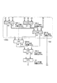
図1は本発明の第1の実施形態に係る演算装置の構成を示す模式図である。この演算装置は、整数加算用の構成の一部を、拡大体加算用の構成として機能させたものである。
Hereinafter, embodiments of the present invention will be described with reference to the drawings.
(First embodiment)
FIG. 1 is a schematic diagram showing a configuration of an arithmetic device according to the first embodiment of the present invention. In this arithmetic unit, a part of the configuration for integer addition is made to function as a configuration for expansion field addition.
ここで、整数加算用の構成は、整数加算用のCSA(加算器)ツリーと、桁上げ伝搬加算器CPA121とを備えている。 Here, the configuration for integer addition includes a CSA (adder) tree for integer addition and a carry propagation adder CPA121.
整数加算用のCSAツリーは、入力された3個以上のデータを互いに加算し、加算結果を表す排他的論理和データと桁上げデータとを出力する複数の桁上げ保存加算器CSA120−1〜120−5が互いに多入力少出力のツリー状に直列接続されてなる。この整数加算用のCSAツリーは、各桁上げ保存加算器CSA120−1〜120−5の和出力(排他的論理和データ)S0〜S4及び桁上げ出力(桁上げデータ)C0〜C4を順次、加算して整数加算を実行するように構成されている。 The CSA tree for integer addition adds a plurality of input data of three or more to each other, and outputs a plurality of carry storage adders CSA 120-1 to 120 that output exclusive OR data and carry data representing the addition result. -5 are connected in series in a tree shape with multiple inputs and outputs. This CSA tree for integer addition sequentially outputs sum outputs (exclusive OR data) S0 to S4 and carry outputs (carry data) C0 to C4 of carry save adders CSA120-1 to 120-5. An integer addition is performed by adding.
各桁上げ保存加算器CSA120−1〜120−5は、例えば図16に示した全加算器を必要なビット数並べたものとなる。例えば4ビットの場合、図2に示す回路構成となる。この場合、各桁上げ保存加算器CSA120−1〜120−5は、X=(X4,X3,X2,X1)、Y=(Y4,Y3,Y2,Y1)、Z=(Z4,Z3,Z2,Z1)の3つの数値データが入力され、和出力としてS=(S4,S3,S2,S1)が出力され、桁上げ出力としてC=(C5,C4,C3,C2)が出力される。 Each carry save adder CSA120-1 to 120-5 is formed by arranging the full adders shown in FIG. For example, in the case of 4 bits, the circuit configuration is as shown in FIG. In this case, each carry save adder CSA120-1 to 120-5 has X = (X4, X3, X2, X1), Y = (Y4, Y3, Y2, Y1), Z = (Z4, Z3, Z2). , Z1) is input, S = (S4, S3, S2, S1) is output as the sum output, and C = (C5, C4, C3, C2) is output as the carry output.
桁上げ伝搬加算器CPA121は、整数加算用のCSAツリー内の最後尾の桁上げ保存加算器CSA120−5の和出力S4と桁上げ出力C0とを加算し、得られた整数加算結果Rを出力するものである。 The carry propagation adder CPA121 adds the sum output S4 and the carry output C0 of the last carry storage adder CSA120-5 in the CSA tree for integer addition, and outputs the obtained integer addition result R To do.
一方、拡大体加算用の構成は、拡大体加算用のCSA(加算器)ツリー120Gと、拡大体加算結果出力部122とを備えている。
On the other hand, the configuration for extension field addition includes a CSA (adder)
ここで、拡大体加算用のCSAツリー120Gは、整数加算用のCSAツリーの一部分として設けられ、先頭から途中までの桁上げ保存加算器CSA120−1〜120−3からなり、当該各桁上げ保存加算器120−1〜120−3から得られる和出力S0〜S2及び桁上げ出力C0〜C2データのうち、和出力S0〜S2のみを互いに加算して拡大体加算を実行するように構成されている。すなわち、拡大体加算用のCSAツリーは、データ入力とCSAの和出力のみで構成されている。
Here, the
拡大体加算結果出力部122は、拡大体加算用のCSAツリーにおける最後尾の桁上げ保存加算器120−3の和出力S2及び桁上げ出力C2のうち、和出力S2のみを拡大体の加算結果RGとして整数加算用のCSAツリーから分岐出力するものである。
The extension field addition
次に、以上のように構成された演算装置の動作を説明する。
始めに、整数の乗算動作と2の拡大体の乗算動作について述べる。
Next, the operation of the arithmetic unit configured as described above will be described.
First, an integer multiplication operation and an extension field multiplication operation of 2 will be described.
図3は2進数7ビットの被乗数データAと、2進数7ビットの乗数データBとの整数乗算の様子を示す模式図である。被乗数データAの各ビットは、それぞれ(a6、a5、a4、a3、a2、a1、a0)と表され、最上位ビットMSBがa6であり、最下位ビットLSBがa0である。同様に乗数データBの各ビットは、最上位ビットから順に(b6、b5、b4、b3、b2、b1、b0)と表される。 FIG. 3 is a schematic diagram showing the state of integer multiplication of binary 7-bit multiplicand data A and binary 7-bit multiplier data B. Each bit of the multiplicand data A is represented as (a6, a5, a4, a3, a2, a1, a0), the most significant bit MSB is a6, and the least significant bit LSB is a0. Similarly, each bit of the multiplier data B is expressed as (b6, b5, b4, b3, b2, b1, b0) in order from the most significant bit.
整数乗算においては、最初に被乗数データAと乗数データBとの各ビットの論理積が行なわれ、部分積データZ0〜Z6が得られる。すなわち、部分積データZi(=A・bi)を得るため、論理積A・bi(i=0〜6)が行なわれる。 In integer multiplication, first, logical product of each bit of multiplicand data A and multiplier data B is performed, and partial product data Z0 to Z6 are obtained. That is, the logical product A · bi (i = 0 to 6) is performed in order to obtain the partial product data Zi (= A · bi).
例えば、部分積データZ0は、乗数データBの最下位ビットb0と被乗数データAとの論理積である。次に、部分積データZiは、左に1ビットずつシフト(2倍)される。それら部分積データZ0〜Z6が、全て加算されることにより、乗算結果R(=A・B)が得られる。 For example, the partial product data Z0 is a logical product of the least significant bit b0 of the multiplier data B and the multiplicand data A. Next, the partial product data Zi is shifted to the left by 1 bit (doubled). The partial product data Z0 to Z6 are all added to obtain a multiplication result R (= A · B).
一方、拡大体の加算では桁上げが起こらない。従って、論理積の後のシフトまでの手順は整数の場合と同じであるが、通常の加算とは異なり、各桁の排他論理和を行なうことで拡大体での乗算が実現される。この加算部分を実現するのが、拡大体加算用のCSAツリー120Gである。
On the other hand, no carry occurs in the addition of the extension field. Therefore, the procedure up to the shift after the logical product is the same as that in the case of an integer. However, unlike ordinary addition, multiplication in an extended field is realized by performing exclusive OR of each digit. The addition portion is realized by the
拡大体加算用のCSAツリー120Gは、整数加算用のCSAツリーの一部であり、全てのデータ入力Z0〜Z6とCSAの和出力S0,S1のみが入力される桁上げ保存加算器CSA120−1〜120−3のみで構成される。
The
各桁上げ保存加算器CSA120−1〜120−3の和出力S0〜S2は、それぞれ3つの入力データの各ビットの排他論理和の結果であり、すなわち、拡大体における加算結果である。従って、拡大体加算用のCSAツリー120Gにおける最後尾の桁上げ保存加算器CSA120−3の和出力S2は、全ての入力の各桁(ビット)の排他論理和の結果となる。従って、拡大体加算用のCSAツリー120Gの出力RGは、拡大体の乗算結果と一致する。
The sum outputs S0 to S2 of the carry save adders CSA 120-1 to 120-3 are the results of exclusive OR of the respective bits of the three input data, that is, the addition results in the extension field. Therefore, the sum output S2 of the last carry save adder CSA120-3 in the
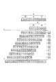
以上のようなCSAツリーの演算過程を図4を用いて詳細に述べる。 The calculation process of the CSA tree as described above will be described in detail with reference to FIG.
乗数データBの各ビットとの部分積データZ0〜Z6が入力データとして本実施形態のCSAツリーに入力される。CSAツリーにおいては、入力された部分積データZ0〜Z2は、桁上げ保存加算器CSA120−1により互いに加算され、加算結果を表す和出力S0及び桁上げ出力C0として桁上げ保存加算器CSA120−1から出力される。同様に、入力された部分積データZ3〜Z5は、桁上げ保存加算器CSA120−2により互いに加算され、加算結果を表す和出力S1及び桁上げ出力C1として桁上げ保存加算器CSA120−2から出力される。 Partial product data Z0 to Z6 with each bit of the multiplier data B are input as input data to the CSA tree of this embodiment. In the CSA tree, the input partial product data Z0 to Z2 are added to each other by a carry save adder CSA120-1, and a carry save adder CSA120-1 is added as a sum output S0 and a carry output C0 representing the addition result. Is output from. Similarly, the input partial product data Z3 to Z5 are added to each other by the carry save adder CSA 120-2, and output from the carry save adder CSA 120-2 as a sum output S1 and a carry output C1 representing the addition result. Is done.
次に、和出力S0,S1及び部分積データZ6は、桁上げ保存加算器CSA120−3により互いに加算され、和出力S2及び桁上げ出力C2として桁上げ保存加算器CSA120−3から出力される。この和出力S2は、部分積データZ0〜Z6の各桁の排他論理和であり、整数加算用のCSAツリーから分岐して、拡大体の乗算結果RGとして出力される。 Next, the sum outputs S0 and S1 and the partial product data Z6 are added to each other by the carry save adder CSA 120-3, and output from the carry save adder CSA 120-3 as the sum output S2 and the carry output C2. This sum output S2 is an exclusive OR of each digit of the partial product data Z0 to Z6, branches from the CSA tree for integer addition, and is output as the multiplication result RG of the extension field.
さらに、桁上げ出力C0〜C2は、桁上げ保存加算器CSA120−4により互いに加算され、和出力S3及び桁上げ出力C3として桁上げ保存加算器CSA120−4から出力される。 Further, the carry outputs C0 to C2 are added to each other by the carry save adder CSA120-4, and are output from the carry save adder CSA120-4 as the sum output S3 and the carry output C3.
そして、和出力S2,S3及び桁上げ出力C3は、桁上げ保存加算器CSA120−5により互いに加算され、和出力S4及び桁上げ出力C4として桁上げ保存加算器CSA120−5から出力される。この和出力S4と桁上げ出力C4は、桁上げ伝播加算器CPA121により互いに加算され、最終的な整数を表す乗算結果Rとして出力される。 The sum outputs S2 and S3 and the carry output C3 are added to each other by the carry save adder CSA120-5, and are output from the carry save adder CSA120-5 as the sum output S4 and the carry output C4. The sum output S4 and the carry output C4 are added together by the carry propagation adder CPA121 and output as a multiplication result R representing the final integer.
上述したように本実施形態によれば、図14に示した全加算器に比べてアンドゲート106が無い分だけ小さい回路で高速演算可能な桁上げ保存加算器CSA120−1〜120−5からなる整数加算用のCSAツリーの一部を和出力S0〜S2のみを加算させるように構成して、整数加算用のCSAツリーの一部を拡大体加算用のCSAツリー120Gとして機能させることにより、整数の演算と拡大体の演算とを小さい回路規模で高速に実行することができる。
As described above, according to the present embodiment, the carry storage adders CSA120-1 to 120-5 that can be operated at high speed with a circuit smaller than the full adder shown in FIG. A part of the CSA tree for integer addition is configured to add only the sum outputs S0 to S2, and a part of the CSA tree for integer addition functions as the
すなわち、入力データZ0〜Z6とCSAの和出力のみを入力とするCSAから構成されるCSAツリー120Gを用いるので、CSAツリー120Gの和出力S2が拡大体の演算結果RGとなり、拡大体演算に関し、桁上げ(キャリー)信号の制御が不要となる。また、CSAツリー120Gの和出力S2は整数加算の途中結果であるので、さらに桁上げ出力C0〜C2を加算することにより、整数の加算結果Rをも得ることができる。すなわち、整数加算用のCSAツリーの一部を拡大体加算用のCSAツリーとして機能させる構成により、回路規模の小型化、高速化を実現することができる。
That is, since the
(第2の実施形態)
次に、本発明の第2の実施形態について説明するが、予めその背景について述べる。暗号処理では、数百ビットから数千ビットの多ワードの乗数データ同士を乗算することがある。この種の多ワードの乗算処理は一度に実行する場合、大規模なハードウェア抜きでは困難である。従って、多ワードの乗算処理は、比較的短いビットの乗算を繰り返して実行される。本実施形態は、このような多ワードの乗算処理にも適用可能な複数ワードの乗算処理に関するものである。
(Second Embodiment)
Next, a second embodiment of the present invention will be described, and the background will be described in advance. In cryptographic processing, multiword multiplier data of several hundred bits to several thousand bits may be multiplied. This type of multi-word multiplication processing is difficult without a large-scale hardware when executed at a time. Therefore, multiword multiplication is performed by repeating relatively short bit multiplication. The present embodiment relates to a multi-word multiplication process applicable to such a multi-word multiplication process.
図5は本発明の第2の実施形態に係る演算装置の構成を示す模式図である。この演算装置は、メモリ140、部分積算出回路141、部分積加算器142−1、加算回路143、排他論理和回路144、選択回路145及び制御部146を備えている。
FIG. 5 is a schematic diagram showing a configuration of an arithmetic device according to the second embodiment of the present invention. The arithmetic unit includes a
メモリ140は、制御部146によりバスを介して読出/書込されるRAMであり、入力データ(被乗数データA、乗数データB)、中間結果C及び最終結果Zがバスを介して一時的に記憶される。
The
部分積算出回路141は、メモリ140からバスを介して転送入力された被乗数データAと乗数データBとの部分積を算出し、得られた部分積データZ0〜Z7を部分積加算器142−1に出力する機能をもっている。
The partial
具体的には、部分積算出回路141は、各データが複数ビットからなり、複数ビットを1ワード単位としたとき、複数ワードからなる被乗数データAに複数ワードからなる乗数データBを乗算する際に、被乗数データAの各ワードと乗数データBの各ワードとを乗算し、乗数データBの各ワード毎に、被乗数データAのワード数と同じ個数の部分積データを算出する機能をもっている。また、部分積算出回路141は、算出した各部分積データZ0〜Z7を加算させるように、各部分積データZ0〜Z7を先頭の桁上げ保存加算器120−1,120−2,120−4に入力する機能(部分積入力手段)をもっている。
Specifically, the partial
部分積加算器142−1は、図1に示したCSAツリーで構成され、部分積算出回路141から入力された部分積データZ0〜Z7の拡大体加算と整数加算とを実行する機能と、得られた整数加算結果Rを加算器143に出力する機能と、得られた拡大体加算結果RGを排他論理和回路144に出力する機能とをもっている。
The partial product adder 142-1 is configured by the CSA tree shown in FIG. 1, and has a function of performing the extended field addition and integer addition of the partial product data Z <b> 0 to Z <b> 7 input from the partial
加算器143は、部分積加算回路142の整数加算結果Rとメモリ140からバスを介して転送入力された中間結果Cとを加算し、得られた加算結果を選択回路145に出力するものである。
The
排他論理和回路144は、部分積加算回路142の拡大体加算結果RGとメモリ140からバスを介して転送入力された中間結果Cとの排他的論理和を算出し、得られた算出結果を選択回路145に出力するものである。
The exclusive OR
選択回路145は、部分積加算器142−1で整数加算を実行するときには加算器143の出力を選択し、部分積加算器142−1で拡大体加算を実行するときには排他論理和回路144の出力を選択し、選択により得られた最終結果データZをメモリ140に向けてバスに出力するものである。
The
制御部146は、前述した各回路140〜145を、被乗数データAと乗数データBとの乗算を実行するように制御するものである。
The
次に、以上のように構成された演算装置の動作を説明する。
図6は12ビットの被乗数データAと8ビットの乗数データBとを乗算する様子を示す概念図である。図6の例では4ビットを1ワードとしている。すなわち、被乗数データAは、3ワードa2,a1,a0で構成される。各ワードは、a2={a23,a22,a21,a20}であり、a1={a13,a12,a11,a10}であり、a0={a03,a02,a01,a00}である。
Next, the operation of the arithmetic unit configured as described above will be described.
FIG. 6 is a conceptual diagram showing a state where 12-bit multiplicand data A and 8-bit multiplier data B are multiplied. In the example of FIG. 6, 4 bits are used as one word. That is, the multiplicand data A is composed of three words a2, a1, and a0. Each word is a2 = {a23, a22, a21, a20}, a1 = {a13, a12, a11, a10}, and a0 = {a03, a02, a01, a00}.
乗数データBは、2ワードb1,b0で構成される。各ワードは、b1={b13,b12,b11,b10}であり、b0={b03,b02,b01,b00}である。 Multiplier data B is composed of two words b1 and b0. Each word is b1 = {b13, b12, b11, b10}, and b0 = {b03, b02, b01, b00}.
この2数A,Bの乗算は、図6に示すように、各ビットの論理積を求め、得られた部分積データを乗数データBのビットの位置によって左にシフトした値を全て加算して実行される。 As shown in FIG. 6, the multiplication of the two numbers A and B is performed by calculating the logical product of each bit and adding all the values obtained by shifting the obtained partial product data to the left by the bit position of the multiplier data B. Executed.
すなわち、被乗数データAと乗数データBの最下位ビットb00との論理積の値(A・b00)、被乗数データAと最下位から2番目ビットb01との論理積(A・b01)を1ビット左シフトした値、…、被乗数データAと最下位から7番目ビットb13との論理積(A・b13)を7ビット左シフトした値、の全てを合計した値が乗算結果となる。 That is, the logical product value (A · b00) of the multiplicand data A and the least significant bit b00 of the multiplier data B, and the logical product (A · b01) of the multiplicand data A and the second least significant bit b01 are left one bit. The result of multiplication is the sum of all the shifted values, ..., the logical product of the multiplicand data A and the seventh bit b13 from the least significant bit (A · b13) left-shifted by 7 bits.
このような乗算A×Bを1ワード分の乗算器を用いて実現する場合の様子を図7に示す。この例では、被乗数データAの1ワードa2,a1又はa0と、乗数データの1ワードb0とを入力とし、2ワードの部分積データを出力する乗算器(部分積算出回路141)を用いる。
FIG. 7 shows a state in which such multiplication A × B is realized by using a multiplier for one word. In this example, a multiplier (partial product calculation circuit 141) that
乗算A×Bの概略としては、被乗数データAと、乗数データBの最下位ワードb0とを乗算し、部分積データg(=A×b0)を得る。次に、被乗数データAと、乗数データBの次のワードb1とを乗算し、部分積データk(=A×b1)を得る。最後に、部分積データg,kを加算することで、乗算結果A×B(=g+k)が得られる。 As an outline of the multiplication A × B, the multiplicand data A is multiplied by the least significant word b0 of the multiplier data B to obtain partial product data g (= A × b0). Next, the multiplicand data A is multiplied by the next word b1 of the multiplier data B to obtain partial product data k (= A × b1). Finally, by adding the partial product data g and k, a multiplication result A × B (= g + k) is obtained.
この乗算を1ワード分の乗算器を用いて実現する場合、部分積データg,kは次のように算出される。ここでは、部分積データgの算出過程を代表例に挙げて述べる。 When this multiplication is realized using a multiplier for one word, the partial product data g and k are calculated as follows. Here, the calculation process of the partial product data g will be described as a representative example.
始めに、制御部146は、メモリ140内の被乗数データAの最下位ワードa0および乗数データBの最下位ワードb0を部分積算出回路141に入力する。部分積算出回路141は、被乗数データAの最下位ワードa0と、乗数データBの最下位ワードb0の各ビットとの論理積を計算する。すなわち、a0(={a03,a02,a01,a00})とb00の論理積、a0(={a03,a02,a01,a00})とb01の論理積、a0(={a03,a02,a01,a00})とb02の論理積、a0(={a03,a02,a01,a00})とb03の論理積が部分積として部分積加算器142−1に入力する。
First, the
続いて、部分積加算器142−1は、入力された部分積を互いに加算し、中間データd={d13,d12,d11,d10,d03,d02,d01,d00}が得られる。 Subsequently, the partial product adder 142-1 adds the input partial products to each other, and intermediate data d = {d13, d12, d11, d10, d03, d02, d01, d00} is obtained.
dの下位4ビット(下位1ワード)は、中間データgの最下位ワード({g03,g02,g01,g00})としてメモリ140に書き込まれる。
The lower 4 bits (lower 1 word) of d are written in the
次に、制御部146は、メモリ140内の被乗数データAの最下位ワードa1および乗数データBの最下位ワードb0を部分積算出回路141に入力する。同様に部分積算出回路141によってa1とb0の部分積が計算され、結果が部分積加算器142−1に入力される。部分積加算器142−1では、入力された部分積を互いに加算し、中間データe=={e13,e12,e11,e10,e03,e02,e01,e00}が得られる。
Next, the
中間データeの下位ワードは、中間データdの上位ワードと加算され,中間結果gの一部({g13,g12,g11,g10})としてメモリに保存される。 The lower word of the intermediate data e is added to the upper word of the intermediate data d, and stored in the memory as a part of the intermediate result g ({g13, g12, g11, g10}).
また、中間データeの下位ワードと中間データdの上位ワードの加算において桁上げが発生するが、これは、中間データeの上位ワードと中間データf(a2とb0の処理の結果)のときに一緒に加算される。 Also, a carry occurs in the addition of the lower word of the intermediate data e and the upper word of the intermediate data d. This occurs when the upper word of the intermediate data e and the intermediate data f (results of processing of a2 and b0). It is added together.
同様にa2とb0の乗算も実行され、中間データgがメモリに保存される。 Similarly, multiplication of a2 and b0 is also executed, and the intermediate data g is stored in the memory.
次にAとb1の乗算が同様に実行される。このとき、制御部146は、メモリ140から中間データgを読み出し、加算器143に入力する。これによって、Aとb1の乗算による中間データkとメモリに保存されていた中間データg(Aとb0の乗算結果)の加算が行われ、最終的な乗算結果c={c43,c42,c41,c40,…,c03,c02,c01,c00}が計算される。
Next, multiplication of A and b1 is performed in the same manner. At this time, the
このように、多ワードの乗算は、小規模な乗算器(1ワード分の部分積算出回路141と部分積加算器142−1)による乗算を繰り返し実行し、得られた部分積データg,kを加算器143が加算することで実現される。ここで、部分積加算器142−1は、第1の実施形態(図1)に示した演算装置であるので、多ワードの乗算においても整数乗算と拡大体の乗算とを実現することができる。また、選択回路145により、整数乗算の結果又は拡大体乗算の結果を選択して出力することができる。
In this way, multi-word multiplication is performed by repeatedly performing multiplication by a small-scale multiplier (partial
上述したように本実施形態によれば、多ワードの乗数データ同士を乗算する際に、得られた部分積データの加算に第1の実施形態の演算装置を用いた構成により、第1の実施形態の効果を多ワードの乗算においても得ることができる。 As described above, according to this embodiment, when multiplying multi-word multiplier data, the first embodiment is implemented by using the arithmetic unit of the first embodiment to add the obtained partial product data. The effect of form can also be obtained in multi-word multiplication.
なお、本実施形態では、図7中、部分積データg(=A×b0),k(=A×b1)を算出した後に、部分積データの加算(g+k)を実行する場合を説明したが、これに限らず、図8に示すように、部分積データkを算出する時に、同時に同じ桁の部分積データgを加算器に入力する構成に変形することができる。この変形例では、部分積加算器142−2は、部分積加算器142−1に比べ、中間結果Cの入力端子が付加されている。 In the present embodiment, the case where partial product data addition (g + k) is executed after calculating partial product data g (= A × b0) and k (= A × b1) in FIG. 7 has been described. Not limited to this, as shown in FIG. 8, when the partial product data k is calculated, the partial product data g having the same digit can be simultaneously inputted to the adder. In this modification, the partial product adder 142-2 has an input terminal for the intermediate result C compared to the partial product adder 142-1.
(第3の実施形態)
次に、本発明の第3の実施形態に係る演算装置について、前述した図5及び新たな図9を参照しながら説明する。図9は同演算装置に適用される部分積加算器の構成を示す模式図であり、前述した要素には同一符号を付してその詳しい説明を省略し、ここでは異なる部分について主に述べる。
(Third embodiment)
Next, an arithmetic unit according to the third embodiment of the present invention will be described with reference to FIG. 5 and the new FIG. FIG. 9 is a schematic diagram showing a configuration of a partial product adder applied to the same arithmetic unit. The above-described elements are denoted by the same reference numerals, detailed description thereof is omitted, and different parts are mainly described here.
すなわち、本実施形態は、第2の実施形態の変形例であり、乗数データA,Bの乗算過程が異なるものである。これに伴い、部分積加算器142−1を図9に示す構成としており、制御部146をこの部分積加算器142−1を制御する機能を有するものとしている。
That is, this embodiment is a modification of the second embodiment, and the multiplication process of the multiplier data A and B is different. Accordingly, the partial product adder 142-1 is configured as shown in FIG. 9, and the
ここで、部分積算出回路141は、各データが複数ビットからなり、複数ビットを1ワード単位としたとき、複数ワードからなる被乗数データAに複数ワードからなる乗数データBを乗算する際に、被乗数データAと乗数データBの各ワードとを当該各ワード内の各ビット毎に乗算し、乗数データBの各ワード毎に、当該各ワード内のビット数と同じ個数の部分積データを算出する機能をもっている。また、部分積算出回路141は、算出した部分積データZ0〜Z7を下位側から1ワードずつ加算するように、各部分積データZ0〜Z7の各ワードを先頭の桁上げ保存加算器120−1,120−2,120−4に入力する機能(部分積入力手段)をもっている。
Here, the partial
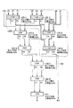
部分積加算器142−1は、図9に示したCSAツリーで構成され、部分積算出回路141から入力された部分積データZ0〜Z7の拡大体加算と整数加算とを実行する機能と、得られた整数加算結果Rを加算器143に出力する機能と、得られた拡大体加算結果RGを排他論理和回路144に出力する機能とをもっている。
The partial product adder 142-1 is configured by the CSA tree shown in FIG. 9, and has a function of executing the extended field addition and integer addition of the partial product data Z <b> 0 to Z <b> 7 input from the partial
図9に示すCSAツリーは、前述同様に、全ての桁上げ保存加算器CSA120−1〜120−8からなる整数加算用のCSAツリーにおいて、この整数加算用のCSAツリーの一部が拡大体加算用のCSAツリー120Gとして機能するように構成されている。また、外部から桁上げ出力CINが2段目の桁上げ保存加算器120−3に入力可能となっている。
The CSA tree shown in FIG. 9 is an integer addition CSA tree composed of all the carry save adders CSA 120-1 to 120-8, as described above, and a part of this integer addition CSA tree is expanded field addition. It is configured to function as a
制御部146は、前述した各回路140〜145を制御するものであり、例えば、桁上げ伝搬加算器121から得られた整数加算結果のうち、1ワードを越えたビットデータを桁上げデータCINとして次の上位側のワードの加算に繰り越すように、部分積算出回路141における部分積データZ0〜Z7の各ワードを先頭の桁上げ保存加算器120−1,120−2,120−4に入力する機能を制御する機能(部分積入力制御手段)をもっている。
The
次に、以上のように構成された演算装置の動作を説明する。
図10は12ビットの被乗数データAと8ビットの乗数データBとを乗算する様子を示す模式図である。4ビットを1ワードとする点は、前述同様である。また、部分積データg(=A×b0)を算出し、次に部分積データk(=A×b1)を算出し、両者を加算するという点も図7と同様である。しかしながら、図10に示した例は、図7と比べ、部分積データg,kを算出する方法が異なっている。図10に示した例では、1ワード毎の乗算を実行せず、加算のみで実現している。
Next, the operation of the arithmetic unit configured as described above will be described.
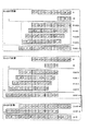
FIG. 10 is a schematic diagram showing a state in which 12-bit multiplicand data A and 8-bit multiplier data B are multiplied. The point that 4 bits are used as one word is the same as described above. Also, the partial product data g (= A × b0) is calculated, the partial product data k (= A × b1) is calculated next, and both are added as in FIG. However, the example shown in FIG. 10 differs from FIG. 7 in the method of calculating the partial product data g and k. In the example shown in FIG. 10, the multiplication for each word is not executed but only the addition is realized.
ここでは、部分積データg(=A×b0)の算出過程を代表例に挙げて述べる。
始めに、制御部146は、メモリ140内の被乗数データA及び乗数データBを部分積算出回路141に入力する。部分積算出回路141は、被乗数データAと、乗数データBの最下位ビットb00との論理積の値(A×b00)を求め、部分積データ(m23,…m00)を得る。次に、被乗数データAと、乗数データBの最下位から2番目ビットb01との論理積の値(A×b01)を求め、部分積データ(n23,…n00)を得る。以下同様に、論理積の値(A×b02)として部分積データ(p23,…p00)と、論理積の値(A×b03)として部分積データ(q23,…q00)とを求める。
Here, the process of calculating the partial product data g (= A × b0) will be described as a representative example.
First, the
すなわち、部分積算出回路141は、被乗数データAと乗数データBの各ワードb0とを当該各ワードb0内の各ビットb00,b01,b02,b03毎に乗算し、乗数データBの各ワードb0毎に、当該各ワードb0内のビット数(=4)と同じ個数(=4)の部分積データを算出する。また、部分積算出回路141は、制御部146からの制御に基づき、算出した部分積データを下位側から1ワードずつ部分積加算器142−1に入力する。
That is, the partial
次に、部分積加算器142−1は、各部分積データ(m23,…m00),(n23,…n00),(p23,…p00),(q23,…q00)を下位から1ワードずつ加算していく。 Next, the partial product adder 142-1 adds each partial product data (m23,... M00), (n23,... N00), (p23,... P00), (q23,. I will do it.
最初に部分積加算器142−1は、下位から1ワード分の部分積データとして(m03,m02,m01,m00)と(n02,n01,n00,0)と(p01,p00,0,0)と(q00,0,0,0)とを加算し、下位から1ワード分の部分積データ(r03,r02,r01,r00)を得る。このとき、桁上げ出力CINが発生するが、桁上げ出力CINは、次の1ワード分の加算に繰り込まれる。 First, the partial product adder 142-1 has (m03, m02, m01, m00), (n02, n01, n00, 0), (p01, p00, 0, 0) as partial product data for one word from the lower order. And (q00,0,0,0) are added to obtain partial product data (r03, r02, r01, r00) for one word from the lower order. At this time, a carry output CIN is generated, but the carry output CIN is carried over to the addition of the next one word.
次に部分積加算器142−1は、下位から2ワード目の1ワード分の部分積データとして(m13,m12,m11,m10)と(n12,n11,n10,n03)と(p11,p10,p03,p02)と(q10,q03,q02,q01)と、下位の1ワードの計算による桁上げ出力CINとを加算し、下位から2ワード目の1ワード分の部分積データ(r13,r12,r11,r10)及び桁上げ出力CINを得る。 Next, the partial product adder 142-1 has (m13, m12, m11, m10), (n12, n11, n10, n03), (p11, p10, p03, p02) and (q10, q03, q02, q01) and the carry output CIN obtained by calculating the lower one word, and the partial product data (r13, r12, r11, r10) and carry output CIN.
以下同様に、部分積加算器142−1は、下位から3ワード目の1ワード分の部分積データ(r23,r22,…,r20)及び桁上げ出力CINを算出し、下位から4ワード目の1ワード分の部分積データ(r33,r32,…,r30)を算出する。そして、これら各部分積データ(r33,r32,…,r30),(r23,r22,…,r20),(r13,r12,…,r10),(r03,r02,…,r00)を連結することにより、最終的に、部分積データg(=A×b0)として(r33,r32,…,r01,r00)が算出される。
Similarly, the partial product adder 142-1 calculates the partial product data (
また同様に、部分積データk(=A×b1)として部分積データ(w33,w32,…,w00)が算出される。そして、部分積加算器142−1は、各部分積データ(r33,r32,…,r00)と(w33,w32,…,w00)とを加算し、乗算結果A×Bを得る。乗算結果A×Bは、選択回路145やバス等を介して制御部146によりメモリ140に書込まれる。
Similarly, partial product data (w33, w32,..., W00) is calculated as partial product data k (= A × b1). Then, the partial product adder 142-1 adds each partial product data (r33, r32,..., R00) and (w33, w32,..., W00) to obtain a multiplication result A × B. The multiplication result A × B is written into the
図10に示すような演算の際に、1ワード分の部分積データを順次加算する構成として図9に示すCSAツリーを用いるため、整数の乗算と拡大体の乗算を実行できる。 Since the CSA tree shown in FIG. 9 is used as a configuration in which partial product data for one word is sequentially added in the calculation shown in FIG. 10, integer multiplication and expansion field multiplication can be executed.
次に、図9に示すCSAツリーによる加算過程を詳細に説明する。なお、図6〜図10は、1ワード4ビットの場合の乗算の例を示したが、図9では、1ワード8ビットの場合の例を示している。また、桁上げ入力CINは、拡大体の演算を実行するCSAツリー120Gには含まれない。
Next, the addition process by the CSA tree shown in FIG. 9 will be described in detail. 6 to 10 show examples of multiplication in the case of 1
図11は図9に示すCSAツリーの動作を説明するための模式図である。図4では、部分積データZ0〜Z6が1ビットずつ左にシフトしていたのに対し、図11では、部分積データZ0〜Z7が同じ桁に配置されている。この理由は、図10に示した乗算方法を用いるためである。 FIG. 11 is a schematic diagram for explaining the operation of the CSA tree shown in FIG. In FIG. 4, the partial product data Z0 to Z6 are shifted to the left by one bit, whereas in FIG. 11, the partial product data Z0 to Z7 are arranged in the same digit. This is because the multiplication method shown in FIG. 10 is used.
最初に、部分積データZ0,Z1,Z2が桁上げ保存加算器CSA120−1に入力され、桁上げ保存加算器CSA120−1から和出力S0、桁上げ出力C0が出力される。また、部分積データZ3,Z4,Z5が桁上げ保存加算器CSA120−2に入力され、桁上げ保存加算器CSA120−2から和出力S1、桁上げ出力C1が出力される。 First, partial product data Z0, Z1, and Z2 are input to carry save adder CSA 120-1, and sum output S0 and carry output C0 are output from carry save adder CSA 120-1. The partial product data Z3, Z4, and Z5 are input to the carry save adder CSA 120-2, and the sum output S1 and the carry output C1 are output from the carry save adder CSA 120-2.
次に、部分積データZ6,Z7及び和出力S1が桁上げ保存加算器CSA120−4に入力され、桁上げ保存加算器CSA120−4から和出力S3、桁上げ出力C3が出力される。また、桁上げ保存加算器CSA120−1の桁上げ出力C0、桁上げ保存加算器CSA120−2の桁上げ出力C1、桁上げ入力CINが桁上げ保存加算器CSA120−3に入力され、桁上げ保存加算器CSA120−3から和出力S2、桁上げ出力C2が出力される。 Next, the partial product data Z6, Z7 and the sum output S1 are input to the carry save adder CSA120-4, and the sum output S3 and the carry output C3 are output from the carry save adder CSA120-4. Also, the carry output C0 of the carry save adder CSA 120-1, the carry output C1 of the carry save adder CSA 120-2, and the carry input CIN are input to the carry save adder CSA 120-3, and the carry save is performed. A sum output S2 and a carry output C2 are output from the adder CSA120-3.
次に、桁上げ保存加算器CSA120−1の和出力S0と、桁上げ保存加算器CSA120−4の和出力S3とがCSA120−6に入力され、桁上げ保存加算器CSA120−6から和出力S5、桁上げ出力C5が出力される。 Next, the sum output S0 of the carry save adder CSA 120-1 and the sum output S3 of the carry save adder CSA 120-4 are input to the CSA 120-6, and the sum output S5 from the carry save adder CSA 120-6. The carry output C5 is output.
CSA120−6の和出力S5は、データ入力Z0〜Z7と途中の和出力のみから計算された和出力であり、拡大体の乗算結果となる。 The sum output S5 of the CSA 120-6 is a sum output calculated only from the data inputs Z0 to Z7 and the sum output on the way, and is the multiplication result of the expansion field.
また、桁上げ保存加算器CSA120−3の桁上げ出力C2、和出力S2、桁上げ保存加算器CSA120−4の桁上げ出力C3がCSA120−5に入力され、和出力S4、桁上げ出力C4が出力される。 Also, the carry output C2 and sum output S2 of the carry save adder CSA120-3 and the carry output C3 of the carry save adder CSA120-4 are input to the CSA 120-5, and the sum output S4 and carry output C4 are obtained. Is output.
次に、桁上げ保存加算器CSA120−5の和出力S4及び桁上げ出力S4と、桁上げ保存加算器CSA120−6の桁上げ出力C5とが桁上げ保存加算器CSA120−7に入力され、和出力S6、桁上げ出力C6が出力される。 Next, the sum output S4 and carry output S4 of the carry save adder CSA 120-5 and the carry output C5 of the carry save adder CSA 120-6 are input to the carry save adder CSA 120-7, Output S6 and carry output C6 are output.
次に、これら和出力S6及び桁上げ出力C6と、桁上げ保存加算器CSA120−6の和出力S5とが桁上げ保存加算器CSA120−8に入力され、桁上げ保存加算器120−8から和出力S7、桁上げ出力C7が出力される。この出力S7,C7が桁上げ伝播加算器121に入力され、桁上げ伝播加算器121から整数の乗算結果Rが出力される。また前述同様に、選択回路145により、整数の乗算結果R又は拡大体の乗算結果RGを選択して出力することができる。
Next, the sum output S6 and carry output C6 and the sum output S5 of the carry save adder CSA 120-6 are input to the carry save adder CSA 120-8, and the sum is output from the carry save adder 120-8. Output S7 and carry output C7 are output. The
上述したように本実施形態によれば、部分積データを1ワード毎に加算するように図9に示したCSAツリーを用いた構成としても、第2の実施形態と同様の効果を得ることができ、整数乗算と拡大体乗算とを実行することができる。 As described above, according to the present embodiment, even if the configuration using the CSA tree shown in FIG. 9 is used to add partial product data for each word, the same effect as in the second embodiment can be obtained. Integer multiplication and extension field multiplication can be performed.
(第4の実施形態)
図12は本発明の第4の実施形態に係る演算装置に適用されるCSAツリーの構成を示す模式図である。
(Fourth embodiment)
FIG. 12 is a schematic diagram showing a configuration of a CSA tree applied to an arithmetic device according to the fourth embodiment of the present invention.
すなわち、本実施形態は、第3の実施形態の変形例であり、セレクタ145を省略する観点から、拡大体の演算結果S5を整数の演算結果C6,S6と合流させる箇所に配置され、合流する予定の整数の演算結果C6,S6を通過又は遮断するアンドゲート(桁上げデータ遮断手段)123を備えている。
In other words, this embodiment is a modification of the third embodiment, and is arranged at a location where the calculation result S5 of the expansion field is merged with the integer calculation results C6 and S6 from the viewpoint of omitting the
アンドゲート123は、整数切替信号を受けると、桁上げ保存加算器120−7の出力C6,S6を通過させて桁上げ保存加算器120−8に入力し、拡大体切替信号を受けると、桁上げ保存加算器120−7の出力C6,S6を遮断してゼロ出力(0値)を桁上げ保存加算器120−8に入力する。
When the AND
これにより、整数切替信号がアンドゲート123に入力中、桁上げ保存加算器120−8では、整数の演算結果C6,S6と拡大体の演算結果S5とを加算し、整数の演算結果を示す出力C7,S7を桁上げ伝搬加算器121に出力する。桁上げ伝搬加算器121では、この出力C7,S7を加算し、整数の演算結果Rを出力する。
As a result, while the integer switching signal is being input to the AND
一方、拡大体切替信号がアンドゲート123に入力中、桁上げ保存加算器120−8では、ゼロ出力(0値)と拡大体の演算結果S5とを加算し、拡大体の演算結果を示す出力C7,S7を桁上げ伝搬加算器121に出力する。桁上げ伝搬加算器121では、この出力C7,S7を加算し、拡大体の演算結果RGを出力する。
従って、整数/拡大体切替信号に応じて、整数の演算結果Rと拡大体の演算結果RGを得ることができる。
On the other hand, while the expansion field switching signal is being input to the AND
Accordingly, an integer calculation result R and an expansion field calculation result RG can be obtained in accordance with the integer / expansion field switching signal.
以上のような構成によれば、選択回路145を省略しつつ、整数の乗算と拡大体の乗算の両方を同一の回路で実現でき、回路の小型化と高速化を実現することができる。
According to the above configuration, both the integer multiplication and the expansion field multiplication can be realized by the same circuit while omitting the
詳しくは、図12に示す構成は、CSAツリー全体で1個のアンドゲート123を必要とするので、回路規模を小型化できる。一方、図14に示す従来の構成は、CSAツリーの各CSA毎にアンドゲート106を必要とするので、回路規模を増大させてしまう。
Specifically, since the configuration shown in FIG. 12 requires one AND
なお、本願発明は上記実施形態そのままに限定されるものではなく、実施段階ではその要旨を逸脱しない範囲で構成要素を変形して具体化できる。また、上記実施形態に開示されている複数の構成要素の適宜な組み合わせにより、種々の発明を形成できる。例えば、実施形態に示される全構成要素から幾つかの構成要素を削除してもよい。さらに、異なる実施形態にわたる構成要素を適宜組み合わせてもよい。 Note that the present invention is not limited to the above-described embodiments as they are, and can be embodied by modifying the constituent elements without departing from the scope of the invention in the implementation stage. In addition, various inventions can be formed by appropriately combining a plurality of components disclosed in the embodiment. For example, some components may be deleted from all the components shown in the embodiment. Furthermore, constituent elements over different embodiments may be appropriately combined.
120−1〜120−8…桁上げ保存加算器(CSA)、120G…拡大体加算用の加算器ツリー、121…桁上げ伝播加算器(CPA)、122…拡大体加算結果出力部、123…アンドゲート、140…メモリ、141…部分積算出回路、142−1,142−2…部分積加算器、143…加算器、144…排他論理和回路、145…選択回路、146…制御部。 120-1 to 120-8 ... carry save adder (CSA), 120G ... adder tree for extension field addition, 121 ... carry propagation adder (CPA), 122 ... extension field addition result output unit, 123 ... AND gate, 140 ... memory, 141 ... partial product calculation circuit, 142-1, 142-2 ... partial product adder, 143 ... adder, 144 ... exclusive OR circuit, 145 ... selection circuit, 146 ... control unit.
Claims (6)
前記整数加算用の加算器ツリーの一部分として設けられ、先頭から途中までの複数の桁上げ保存加算器からなり、当該各桁上げ保存加算器から得られる排他的論理和データ及び桁上げデータのうち、排他的論理和データのみを互いに加算して拡大体加算を実行するように構成された拡大体加算用の加算器ツリーと、
前記拡大体加算用の加算器ツリーにおける最後尾の桁上げ保存加算器の排他的論理和データ及び桁上げデータのうち、排他的論理和データのみを拡大体の加算結果として前記整数加算用の加算器ツリーから分岐出力する拡大体加算結果出力手段と、
前記各データが複数ビットからなり、前記複数ビットを1ワード単位としたとき、複数ワードからなる被乗数データに複数ワードからなる乗数データを乗算する際に、前記被乗数データと前記乗数データの各ワードとを当該各ワード内の各ビット毎に乗算し、前記乗数データの各ワード毎に、当該各ワード内のビット数と同じ個数の部分積データを算出する部分積算出回路と、
前記部分積算出回路により得られた各部分積データを下位側から1ワードずつ加算するように、各部分積データの各ワードを前記先頭の桁上げ保存加算器に入力する部分積入力手段と、
前記部分積入力手段による入力の結果、前記整数加算用の加算器ツリー内の最後尾の桁上げ保存加算器から得られる排他的論理和データと桁上げデータとを加算し、得られた整数加算結果を出力する桁上げ伝搬加算器と、
前記桁上げ伝搬加算器から得られた整数加算結果のうち、1ワードを越えたビットデータを桁上げデータとして次の上位側のワードの加算に繰り越すように、前記部分積入力手段を制御する部分積入力制御手段と、
を備えたことを特徴とする演算装置。 Multiple carry save adders that add three or more input data to each other and output exclusive OR data representing the addition result and carry data are connected in series in a tree form of multiple inputs and small outputs. An arithmetic unit comprising an adder tree for integer addition configured to sequentially add the exclusive OR data and the carry data to perform integer addition,
Provided as part of the adder tree for integer addition, consisting of a plurality of carry save adders from the beginning to the middle, among exclusive OR data and carry data obtained from each carry save adder An adder tree for extension field addition configured to perform addition field addition by adding only exclusive OR data to each other;
Of the exclusive OR data and carry data of the last carry save adder in the adder tree for the extension field addition, the addition for the integer addition is performed using only the exclusive OR data as the addition result of the extension field. Expansion field addition result output means for branching out from the container tree;
When each data is composed of a plurality of bits and the plurality of bits are in units of one word, the multiplicand data composed of a plurality of words is multiplied by the multiplier data composed of a plurality of words. For each bit in each word, and for each word of the multiplier data, a partial product calculation circuit for calculating the same number of partial product data as the number of bits in each word;
Partial product input means for inputting each word of each partial product data to the leading carry save adder so that each partial product data obtained by the partial product calculation circuit is added word by word from the lower order side;
As a result of the input by the partial product input means, the exclusive OR data obtained from the last carry save adder in the adder tree for integer addition and the carry data are added, and the obtained integer addition A carry propagation adder that outputs the result;
A portion for controlling the partial product input means so that bit data exceeding one word is carried over to the next higher word addition as carry data among the integer addition results obtained from the carry propagation adder Product input control means;
An arithmetic device comprising:
前記整数加算用の加算器ツリーの一部分として設けられ、先頭から途中までの複数の桁上げ保存加算器からなり、当該各桁上げ保存加算器から得られる排他的論理和データ及び桁上げデータのうち、排他的論理和データのみを互いに加算して拡大体加算を実行するように構成された拡大体加算用の加算器ツリーと、
前記拡大体加算用の加算器ツリーにおける最後尾の桁上げ保存加算器の排他的論理和データ及び桁上げデータのうち、排他的論理和データのみを拡大体の加算結果として前記整数加算用の加算器ツリーから分岐出力する拡大体加算結果出力手段と、
前記各データが複数ビットからなり、前記複数ビットを1ワード単位としたとき、複数ワードからなる被乗数データに複数ワードからなる乗数データを乗算する際に、前記被乗数データの各ワードと前記乗数データの各ワードとを乗算し、前記乗数データの各ワード毎に、前記被乗数データのワード数と同じ個数の部分積データを算出する部分積算出回路と、
前記部分積算出回路により得られた各部分積データを加算するように、当該各部分積データを前記先頭の桁上げ保存加算器に入力する部分積入力手段と、
前記部分積入力手段による入力の結果、前記整数加算用の加算器ツリー内の最後尾の桁上げ保存加算器から得られる排他的論理和データと桁上げデータとを加算し、得られた整数加算結果を出力する桁上げ伝搬加算器と、
を備えたことを特徴とする演算装置。 Multiple carry save adders that add three or more input data to each other and output exclusive OR data representing the addition result and carry data are connected in series in a tree form of multiple inputs and small outputs. An arithmetic unit comprising an adder tree for integer addition configured to sequentially add the exclusive OR data and the carry data to perform integer addition,
Provided as part of the adder tree for integer addition, consisting of a plurality of carry save adders from the beginning to the middle, among exclusive OR data and carry data obtained from each carry save adder An adder tree for extension field addition configured to perform addition field addition by adding only exclusive OR data to each other;
Of the exclusive OR data and carry data of the last carry save adder in the adder tree for the extension field addition, the addition for the integer addition is performed using only the exclusive OR data as the addition result of the extension field. Expansion field addition result output means for branching out from the container tree;
When each data is composed of a plurality of bits and the plurality of bits are in units of one word, when multiplying multiplicand data composed of a plurality of words by multiplier data composed of a plurality of words, each word of the multiplicand data and the multiplier data A partial product calculation circuit that multiplies each word and calculates, for each word of the multiplier data, the same number of partial product data as the number of words of the multiplicand data;
Partial product input means for inputting each partial product data to the leading carry save adder so as to add each partial product data obtained by the partial product calculation circuit;
As a result of the input by the partial product input means, the exclusive OR data obtained from the last carry save adder in the adder tree for integer addition and the carry data are added, and the obtained integer addition A carry propagation adder that outputs the result;
An arithmetic device comprising:
整数加算を実行するときには前記桁上げ伝搬加算器から得られる整数加算結果を選択し、拡大体加算を実行するときには前記拡大体加算結果出力手段から得られる拡大体の加算結果を選択するための選択手段を備えたことを特徴とする演算装置。 In the arithmetic unit according to claim 1 or 2 ,
Selection for selecting the integer addition result obtained from the carry propagation adder when performing integer addition, and selecting the addition result of the extension field obtained from the extension field addition result output means when executing extension field addition A computing device comprising means.
前記拡大体加算結果出力手段に代えて、
整数加算を実行するときには前記整数加算用の加算器ツリー内の最後尾の桁上げ保存加算器に入力される桁上げデータを通過させ、拡大体加算を実行するときには当該最後尾の桁上げ保存加算器に入力される桁上げデータを遮断するための桁上げデータ遮断手段を備えたことを特徴とする演算装置。 In the arithmetic unit according to claim 1 or 2 ,
Instead of the expanded field addition result output means,
When performing integer addition, the carry data input to the last carry save adder in the adder tree for integer addition is passed, and when performing extended field addition, the last carry save addition is performed. An arithmetic device comprising a carry data blocking means for blocking carry data input to a device.
前記拡大体加算結果出力手段に代えて、
前記拡大体加算用の加算器ツリー内の最後尾の桁上げ保存加算器から排他的論理和データが入力される桁上げ保存加算器に対して他の桁上げ保存加算器から入力される排他的論理和データ及び桁上げデータに関し、整数加算を実行するときには当該排他的論理和データ及び桁上げデータを通過させ、拡大体加算を実行するときには当該排他的論理和データ及び桁上げデータを遮断するための桁上げデータ遮断手段を備えたことを特徴とする演算装置。 In the arithmetic unit according to claim 1 or 2 ,
Instead of the expanded field addition result output means,
Exclusive input from other carry save adders to carry save adders to which exclusive OR data is input from the last carry save adder in the adder tree for extension field addition With respect to logical sum data and carry data, when executing integer addition, the exclusive logical sum data and carry data are passed, and when executing extended field addition, the exclusive logical sum data and carry data are blocked. An arithmetic device comprising a carry data blocking means.
前記拡大体加算結果出力手段に代えて、
前記拡大体加算用の加算器ツリー内の最後尾の桁上げ保存加算器から桁上げデータが入力される桁上げ保存加算器に関し、整数加算を実行するときには当該桁上げ保存加算器から出力される排他的論理和データ及び桁上げデータを通過させ、拡大体加算を実行するときには当該桁上げ保存加算器から出力される排他的論理和データ及び桁上げデータを遮断するための桁上げデータ遮断手段を備えたことを特徴とする演算装置。 In the arithmetic unit according to claim 1 or 2 ,
Instead of the expanded field addition result output means,
A carry save adder to which carry data is input from the last carry save adder in the adder tree for extension field addition, and is output from the carry save adder when performing integer addition. Carry data blocking means for blocking the exclusive OR data and carry data output from the carry storage adder when passing the exclusive OR data and carry data and executing the extension field addition Arithmetic apparatus characterized by comprising.
Priority Applications (1)
| Application Number | Priority Date | Filing Date | Title |
|---|---|---|---|
| JP2004107646A JP3898705B2 (en) | 2004-03-31 | 2004-03-31 | Arithmetic unit |
Applications Claiming Priority (1)
| Application Number | Priority Date | Filing Date | Title |
|---|---|---|---|
| JP2004107646A JP3898705B2 (en) | 2004-03-31 | 2004-03-31 | Arithmetic unit |
Publications (2)
| Publication Number | Publication Date |
|---|---|
| JP2005293256A JP2005293256A (en) | 2005-10-20 |
| JP3898705B2 true JP3898705B2 (en) | 2007-03-28 |
Family
ID=35326114
Family Applications (1)
| Application Number | Title | Priority Date | Filing Date |
|---|---|---|---|
| JP2004107646A Expired - Fee Related JP3898705B2 (en) | 2004-03-31 | 2004-03-31 | Arithmetic unit |
Country Status (1)
| Country | Link |
|---|---|
| JP (1) | JP3898705B2 (en) |
-
2004
- 2004-03-31 JP JP2004107646A patent/JP3898705B2/en not_active Expired - Fee Related
Also Published As
| Publication number | Publication date |
|---|---|
| JP2005293256A (en) | 2005-10-20 |
Similar Documents
| Publication | Publication Date | Title |
|---|---|---|
| JP3595171B2 (en) | Microprocessor | |
| EP1014274A1 (en) | Neuroprocessor, device for calculating saturation functions, calculation device and adder | |
| US20030200237A1 (en) | Serial operation pipeline, arithmetic device, arithmetic-logic circuit and operation method using the serial operation pipeline | |
| JPH07210369A (en) | Circuit and method for execution of parallel addition and average operation | |
| EP1049025A1 (en) | Method and apparatus for arithmetic operation | |
| JP6350111B2 (en) | Multiplier circuit and multiplication method thereof | |
| JP7435602B2 (en) | Computing equipment and computing systems | |
| JPH0850575A (en) | Programmable processor,method for execution of digital signal processing by using said programmable processor and its improvement | |
| CN113485751A (en) | Method for performing Galois field multiplication, arithmetic unit and electronic device | |
| US5957996A (en) | Digital data comparator and microprocessor | |
| US8275822B2 (en) | Multi-format multiplier unit | |
| US6209012B1 (en) | System and method using mode bits to support multiple coding standards | |
| JPH08123769A (en) | Parallel processor | |
| JP3652518B2 (en) | SIMD type arithmetic unit and arithmetic processing unit | |
| JP2005293256A (en) | Arithmetic unit | |
| JP3579087B2 (en) | Arithmetic unit and microprocessor | |
| JP3660075B2 (en) | Dividing device | |
| US6202078B1 (en) | Arithmetic circuit using a booth algorithm | |
| JP3982965B2 (en) | Iterative and array multipliers | |
| US20080071852A1 (en) | Method to perform a subtraction of two operands in a binary arithmetic unit plus arithmetic unit to perform such a method | |
| JP4255475B2 (en) | Data-driven information processing device | |
| JP3252954B2 (en) | Multiplication method and multiplication circuit | |
| JPH056263A (en) | Adder and absolute value calculation circuit using the adder | |
| KR100900790B1 (en) | Method and Apparatus for arithmetic of configurable processor | |
| WO2020084694A1 (en) | Computation processing device and computation processing device control method |
Legal Events
| Date | Code | Title | Description |
|---|---|---|---|
| A977 | Report on retrieval |
Free format text: JAPANESE INTERMEDIATE CODE: A971007 Effective date: 20060718 |
|
| A131 | Notification of reasons for refusal |
Free format text: JAPANESE INTERMEDIATE CODE: A131 Effective date: 20060725 |
|
| A521 | Written amendment |
Free format text: JAPANESE INTERMEDIATE CODE: A523 Effective date: 20060906 |
|
| TRDD | Decision of grant or rejection written | ||
| A01 | Written decision to grant a patent or to grant a registration (utility model) |
Free format text: JAPANESE INTERMEDIATE CODE: A01 Effective date: 20061219 |
|
| A61 | First payment of annual fees (during grant procedure) |
Free format text: JAPANESE INTERMEDIATE CODE: A61 Effective date: 20061221 |
|
| FPAY | Renewal fee payment (event date is renewal date of database) |
Free format text: PAYMENT UNTIL: 20110105 Year of fee payment: 4 |
|
| FPAY | Renewal fee payment (event date is renewal date of database) |
Free format text: PAYMENT UNTIL: 20120105 Year of fee payment: 5 |
|
| FPAY | Renewal fee payment (event date is renewal date of database) |
Free format text: PAYMENT UNTIL: 20130105 Year of fee payment: 6 |
|
| LAPS | Cancellation because of no payment of annual fees |