JP3896175B2 - Current limiting device - Google Patents
Current limiting device Download PDFInfo
- Publication number
- JP3896175B2 JP3896175B2 JP14634496A JP14634496A JP3896175B2 JP 3896175 B2 JP3896175 B2 JP 3896175B2 JP 14634496 A JP14634496 A JP 14634496A JP 14634496 A JP14634496 A JP 14634496A JP 3896175 B2 JP3896175 B2 JP 3896175B2
- Authority
- JP
- Japan
- Prior art keywords
- current limiting
- limiting device
- current
- conductive
- composite material
- Prior art date
- Legal status (The legal status is an assumption and is not a legal conclusion. Google has not performed a legal analysis and makes no representation as to the accuracy of the status listed.)
- Expired - Fee Related
Links
Images


Classifications
-
- H—ELECTRICITY
- H01—ELECTRIC ELEMENTS
- H01H—ELECTRIC SWITCHES; RELAYS; SELECTORS; EMERGENCY PROTECTIVE DEVICES
- H01H9/00—Details of switching devices, not covered by groups H01H1/00 - H01H7/00
- H01H9/30—Means for extinguishing or preventing arc between current-carrying parts
- H01H9/46—Means for extinguishing or preventing arc between current-carrying parts using arcing horns
- H01H9/465—Shunt circuit closed by transferring the arc onto an auxiliary electrode
-
- H—ELECTRICITY
- H01—ELECTRIC ELEMENTS
- H01C—RESISTORS
- H01C7/00—Non-adjustable resistors formed as one or more layers or coatings; Non-adjustable resistors made from powdered conducting material or powdered semi-conducting material with or without insulating material
- H01C7/02—Non-adjustable resistors formed as one or more layers or coatings; Non-adjustable resistors made from powdered conducting material or powdered semi-conducting material with or without insulating material having positive temperature coefficient
- H01C7/027—Non-adjustable resistors formed as one or more layers or coatings; Non-adjustable resistors made from powdered conducting material or powdered semi-conducting material with or without insulating material having positive temperature coefficient consisting of conducting or semi-conducting material dispersed in a non-conductive organic material
-
- H—ELECTRICITY
- H01—ELECTRIC ELEMENTS
- H01C—RESISTORS
- H01C7/00—Non-adjustable resistors formed as one or more layers or coatings; Non-adjustable resistors made from powdered conducting material or powdered semi-conducting material with or without insulating material
- H01C7/10—Non-adjustable resistors formed as one or more layers or coatings; Non-adjustable resistors made from powdered conducting material or powdered semi-conducting material with or without insulating material voltage responsive, i.e. varistors
- H01C7/12—Overvoltage protection resistors
-
- H—ELECTRICITY
- H02—GENERATION; CONVERSION OR DISTRIBUTION OF ELECTRIC POWER
- H02H—EMERGENCY PROTECTIVE CIRCUIT ARRANGEMENTS
- H02H9/00—Emergency protective circuit arrangements for limiting excess current or voltage without disconnection
- H02H9/02—Emergency protective circuit arrangements for limiting excess current or voltage without disconnection responsive to excess current
- H02H9/026—Current limitation using PTC resistors, i.e. resistors with a large positive temperature coefficient
-
- H—ELECTRICITY
- H01—ELECTRIC ELEMENTS
- H01H—ELECTRIC SWITCHES; RELAYS; SELECTORS; EMERGENCY PROTECTIVE DEVICES
- H01H33/00—High-tension or heavy-current switches with arc-extinguishing or arc-preventing means
- H01H33/02—Details
- H01H33/04—Means for extinguishing or preventing arc between current-carrying parts
- H01H33/16—Impedances connected with contacts
- H01H33/161—Variable impedances
- H01H2033/163—Variable impedances using PTC elements
Landscapes
- Engineering & Computer Science (AREA)
- Microelectronics & Electronic Packaging (AREA)
- Physics & Mathematics (AREA)
- Electromagnetism (AREA)
- Power Engineering (AREA)
- Chemical & Material Sciences (AREA)
- Dispersion Chemistry (AREA)
- Ceramic Engineering (AREA)
- Thermistors And Varistors (AREA)
- Emergency Protection Circuit Devices (AREA)
- Fuses (AREA)
- Arc-Extinguishing Devices That Are Switches (AREA)
Description
【0001】
【産業上の利用分野】
本発明は、一般に、配電やモータ制御用途などの一般的な回路保護に適当な装置に関し、特に、種々の用途に合わせて製造することが可能な、簡単で、再使用可能な、低コストの装置に関する。さらに詳しくは、本発明は、システム電圧が100V以上で短絡電流が100A以上の比較的大電力の用途に適した、導電性複合材料および不均質な抵抗分布構造を用いる電流制限装置に関する。
【0002】
【従来の技術】
短絡が起こったときに回路に流れる電流を制限することができる装置は多数ある。現在用いられている電流制限装置には、通常PTCR(正の抵抗温度係数)またはPTC効果と呼ばれる効果を有する充填材入りポリマー材料を含むものがある。PTCRまたはPTC効果の特質として、ある特定のスイッチ温度で、PTCR材料が比較的導電性から比較的抵抗性への変態を生じる。従来の電流制限装置の中には、PTCR材料(代表的にはカーボンブラック充填ポリエチレン)を加圧接触電極間に配置しているものがある。
【0003】
使用時には、このような従来の電流制限装置は、保護すべき回路に配置される。正常な回路条件下では、電流制限装置は高導電性状態にある。短絡が起こったとき、PTCR材料は抵抗加熱により発熱し、ついには温度がスイッチ温度を越える。この時点で、PTCR材料の抵抗が高抵抗状態に変わり、短絡電流が制限される。短絡状態がなくなると、電流制限装置はスイッチ温度以下まで冷却して、高導電性状態に戻る。高導電性状態の電流制限装置は、将来の短絡発生に応答して再び高抵抗状態に切りかわることができる。
【0004】
米国特許第5,382,938号に、正の温度係数の抵抗率を有する導電性ポリマー組成物の本体と、該本体を通して電流を流すために本体の2つの平行な端面と接触して配置された2つの電極とを備えるPTC素子が記載されている。本体のポリマー組成物は、ポリマー材料に導電性粉末材料を分布させたものである。用語「PTC素子」は、米国特許第5,382,938号の第1図に示されているように、スイッチ温度で正の抵抗温度係数を示す素子についての用語として認められている。本体の平行な表面の少なくとも一方は、電極と、あるいは導電性ポリマー組成物の別の本体の平行な表面と自由接触関係にある。加圧装置により、本体(1つまたは複数)の平行な表面に垂直な方向に圧力を電極に対して加える。可圧装置には、弾性能力を有する圧力印加装置を設けるのが好ましい。PTC素子は、低抵抗状態から高抵抗状態に変化した後、初期抵抗に復帰するので、短絡電流を受けた後でも再利用できる。ポリマー組成物の本体(1つまたは複数)の平行な表面は同心とするのがよい。PTC素子は電気回路に過電流保護の目的で使用される。
【0005】
米国特許第5,313,184号に、抵抗器本体を2つの接触端子間に配置してなる電気抵抗器が記載されている。この抵抗器コアはPTC挙動を示す素子を含み、この素子は、材料に特有の温度以下で、2つの接触端子間に導電通路を形成する。抵抗器は簡単かつ安価とすることができるが、それでも局部的過電圧および全体的過電圧に対して保護された高定格の電流導通容量を有する。このことは、抵抗器コアにバリスタ挙動を呈する材料を追加含有させることにより達成される。バリスタ材料は、少なくとも1つのバリスタを形成するように導電通路の少なくとも1つのサブセクションと並列に接続され、かつ該少なくとも1つのサブセクションを形成するPTC材料の部分と電気的に密着関係に置かれる。PTC挙動を有する素子とバリスタとの並列接続は、ミクロな構成およびマクロな配置の両方により実現することができる。
【0006】
欧州特許0,640,995A1には、2つの平行な平面電極間に配置された、PTC特性を有する抵抗材料を含み、両電極に圧力を加えるようにした電気抵抗素子が記載されている。抵抗材料は、導電性粒子からなる2種の充填成分をポリマー母材に埋設して構成される。短絡電流が生じた場合、電極に接していて、2種の充填成分の内の少なくとも第1充填成分を含有する表面層において、抵抗材料の抵抗率が制限温度値以上でステップ状すなわち階段状に変化する。2種の充填成分の内の第2充填成分を適切に選択して、少なくともポリマー母材と第2充填成分を含有する複合材料が、表面層より1桁以上大きい階段状変化特性を持つPTC特性を示すようにする。同時に、この複合材料の抵抗率は、ポリマー母材と第1充填成分から形成される複合材料より1桁以上低い。
【0007】
上述の方策はすべてPTC挙動を利用して、一層簡単で一層耐久性の高い電流制限装置を得ようとしたものであるが、配電およびモータ制御用途における全般的回路保護に適していて、種々の用途に合わせて製作することが可能な、更に簡単で、更に耐久性が高く、再使用可能な、低コストの電流制限装置が依然として必要とされている。このような装置は、回路を少なくとも2回の短絡、好ましくは多数回の短絡から保護すること、材料がPTCR効果を示すことを必要としないこと、そして100−500ボルトまたはそれ以上の高電圧で使用できることが、要求される。
【0008】
【発明の概要】
電流制限装置は、多くの用途において、電気回路内の敏感な構成要素を大きな故障電流から保護する目的で使用される。用途は、低電圧/電流回路から高電圧/電流配電システムにまで及ぶ。本発明は、種々の用途に合わせて製作することができる、簡単で、再使用可能な、低コストの電流制限装置を提供する。
【0009】
本発明によれば、PTC効果を持たない、導電性充填材を含有する導電性複合材料と、前記複合材料に対して作動的に配置された少なくとも2つの電極と、外側電極間に作動的に配置された不均質な抵抗分布と、前記導電性複合材料に圧縮圧力を加える手段とを備える電流制限装置が提供される。
したがって、本発明の目的は、なんらPTC効果を示さない材料からなる電流制限装置を提供することにある。
【0010】
本発明の他の目的や効果は、図面を参照にした以下の詳細な説明から明らかになろう。
【0011】
【詳しい説明】
本発明の電流制限装置は、熱分解温度または蒸発温度の低いバインダと導電性充填材を含む複合材料を、不均質な抵抗分布構造と組み合わせて使用する。バインダは、低温(<800°C)で有意なガス発生が起こるようなものを選ぶ必要がある。不均質な抵抗分布構造は、代表的には、電流制限装置の少なくとも1つの薄層が電流制限装置の残部よりはるかに高い抵抗をもつように選ばれる。
【0012】
理論に縛られるつもりはないが、本発明のすぐれた効果が得られるのは、短絡が生じているときに、この薄層の断熱抵抗加熱に続いて、急速な熱膨張が生じると共にバインダ材料からガスが発生することにより、上記薄層の所で電流制限装置の部分的または完全な物理的分離が生じ、この結果、電流に対して装置全体の抵抗がより大きくなるためである、と考えられる。こうして、電流制限装置は短絡電流通路に流れる電流を制限する。外部手段により短絡が除かれたとき、電流制限装置は、電流制限装置に組込まれた圧縮圧力により、低抵抗状態に戻って、電流を平常に流れさすことができるようになる。本発明の電流制限装置は、特に各短絡の過酷さや長さのような要因にもよるが、このような短絡条件に対して多数回再使用することができる。
【0013】
本発明をさらに明瞭にするために、以下に好適な実施態様と実施例を説明するが、これらの実施例は本発明の使用例を示しているにすぎない。本発明の1実施態様によれば、導電性複合材料を用いて、装置全体に不均質な抵抗分布が生じるように、電流制限装置を構成する。この装置が再使用可能な電流制限装置として適切に働くためには、電流制限装置の少なくとも1つの薄層を電流の流れ方向に直角に位置し、装置内の同じ寸法および配向の平均層の平均抵抗よりはるかに大きな抵抗をもつようにして、不均質な抵抗分布を形成しなければならない。さらに、電流制限装置は、選ばれた高抵抗薄層に垂直な方向に圧縮圧力をかけなければならない。
【0014】
本発明による電流制限装置の1例では、熱分解温度の低いバインダおよび導電性充填材を有する高導電性複合材料を電極に圧接して、複合材料と電極(片方または両方)との間に有意な接触抵抗があるようにする。使用時には、電流制限装置を、保護すべき電気回路と直列に配置する。正常作動中は、電流制限装置の抵抗は低い(この例では、電流制限装置の抵抗は、高導電性複合材料の抵抗と電極の抵抗と接触抵抗との和に等しい)。短絡が起こると、高電流密度の電流が装置に流れ始める。短絡の初期段階では、装置の抵抗加熱が断熱的であると考えられる。したがって、電流制限装置の抵抗の大きい選ばれた薄層は電流制限装置の残部よりはるかに速く発熱すると考えられる。薄層が適切に設計されていれば、この薄層が十分急速に発熱し、薄層の熱膨張および/または薄層からのガス発生により、薄層の所で電流制限装置内に分離が生じると考えられる。
【0015】
代表的な電流制限装置においては、複合材料の蒸発および/またはアブレーション(ablation)により電極が複合材料から離れると考えられる。この分離状態で、複合材料のアブレーションが起こり、電流制限装置の分離された層間にアークが発生すると考えられる。しかし、分離状態での全抵抗は非分離状態での抵抗よりはるかに大きい。この大きなアーク抵抗は、複合材料のバインダからのガス発生により界面に発生した高い圧力とガスの消イオン特性とが組み合わさるためであると考えられる。いずれにしても、本発明の電流制限装置は、回路の他の構成要素が短絡により破壊されないように、短絡電流を制限するのに有効である。
【0016】
短絡電流を遮断した後、本発明の電流制限装置は、適切に設計されていれば、圧縮圧力が分離された層を互いに押し付けるように作用するため、非分離状態に戻る、つまり復旧すると考えられる。ひとたび電流制限装置の複数の層が非分離状態、すなわち低抵抗状態に戻ってしまえば、電流制限装置は、将来他の短絡導体に応答して電流制限作用を行うのに完全な準備ができた状態にある。
【0017】
本発明の別の実施態様の電流制限装置は、抵抗器、バリスタまたは他の直線性または非直線性素子を含む並列電流通路を用いて、特定の回路において電流制限装置の両端間に現れ得る最大電圧を制御し、或いは回路エネルギの一部を通す別の通路を形成して電流制限装置の有効な寿命を延長するように構成することができる。
【0018】
[実施例1]
本発明の効果を実証するために、図1に示すような電流制限装置を作製した。導電性複合材料は、バインダ材料としてのエラストマ、たとえばシリコーンエラストマと、充填材としての金属、たとえば銀とからなり、その抵抗率は約0.004Ω−cmであった。銀充填硬化性シリコーン材料(エラストマ)を、2成分AおよびBを混合することにより製造した。成分Aは、末端ジメチルビニルシロキシ単位とジメチルシロキシ単位を有し、粘度が25°Cで400cpsであるビニルシリコーンオルガノポリシロキサン流体(23g)と、アメス・ゴールドスミス社(Ames Goldsmith Corp.)から市販されている銀粒子であるAg4300(46.6g)、Ag1036(37.3g)およびAg1024(37.3g)と、珪素に結合した化学結合水素約0.8重量%を有する流体を与えるように末端トリメチルシロキシ単位を有するシリコーンハイドライドシロキサン流体(1g)とから構成した。成分Bは、末端ジメチルビニルシロキシ単位とジメチルシロキシ単位を有し、粘度が400cpsであるビニルシリコーンオルガノポリシロキサン流体(2g)と、ジメチルマレエート(14μl)と、クラステッド(Karstedt)白金触媒(白金の5%キシレン溶液として83μl)(詳しくは、米国特許第3,775,452号参照)とから構成した。成分A(40g)と成分B(0.44g)を混合して、モールドに注入した後、カーバー(Carver)プレスで150°C、圧力5000ポンドにて30分間硬化させた。
【0019】
電極をニッケル電気メッキ銅から作製し、複合材料に圧接させた。なお、導電性複合材料も電極材料もPTCRスイッチング効果を示さない。電極は直径約1/4インチであった。これらの電極を、直径3/4インチ、厚さ約1/8インチの複合材料の中心に配置した。両電極間に約3.7kgの力を加えて圧力を加えた(圧力は約170psiとなった)。本例の電流制限装置は、装置に約30A未満の電流を流したとき、約0.06Ωの抵抗値を有する簡単な抵抗器として機能した。
【0020】
図2に、短絡条件のシミュレーションに用いた電圧パルスを示す。電圧は、最初の約1ミリ秒の間、正常回路動作をシミュレーションするために約2.5Vである。つぎに電圧は、短絡条件のシミュレーションのために、約3ミリ秒の間、約100Vにジャンプする。次に電圧は、短絡の是正のシミュレーションのために約4ミリ秒で約2.5Vまで降下する。
【0021】
図3に、図2に示す電圧パルスを電流制限装置に印加したときに、電流制限装置に流れる電流と同装置の両端間に現れる電圧を示す。
図4は、図3の短絡のシミュレーションの初期部分の拡大図である。電圧が約100Vに跳ね上がるとき、電流が約190Aに跳ね上がり、次いで急激に約1Aの低い値まで降下し、その後パルスの残りの期間その低い値に留まる。したがって、電流は約1667A(100V/0.06Ω)の予測値から1A以下の値に制限されている。
【0022】
図5は電流制限装置の抵抗を時間の関数として示すグラフである。約100Vのパルスがサンプルの電流制限装置に印加されたとき、抵抗が3000倍以上変化することがわかる。このパルス試験の終了後、電流制限装置の抵抗が約0.06Ωの初期値に戻った(30Aの電流プローブを用いて測定した)。したがって、本電流制限装置は次の電流制限動作を待つ準備ができている。実際、この電流制限装置に、さらに3回の電流制限動作を行わせたところ、いかなる種類の故障も生じなかった。材料および電極両方の損傷の程度が低かったので、この電流制限装置がこれ以上多くの回数で働かないと考える理由は認められない。
【0023】
[実施例2]
好適な導電性複合材料を用いて本発明に従って構成した別の電流制限装置の例の動作特性を図6乃至9に示す。本例では、図1に示す電流制限装置構造を使用し、複合材料は、熱硬化性バインダ、たとえばエポキシ・テクノロジイ社(Epoxy−Technology Inc.)から商品名N30として市販されているエポキシバインダと、導電性充填材としての金属、たとえばニッケル粉末とからなる。この複合材料は抵抗率が約0.02乃至0.03Ω−cmで、PTCR効果を示さない。物理的には、本例の装置では、直径約1/4インチのニッケル電気メッキ銅電極を使用し、これらを直径3/4インチ、厚さ約1/8インチの複合材料の中心に配置した。両電極間に約8.2kgの力を加えて圧力を加えた(圧力は約370psiとなった)。本例の電流制限装置は、装置に約30A未満の電流を流したとき、約0.1Ωの抵抗値を有する簡単な抵抗器として機能した。
【0024】
図6に、短絡条件をシミュレーションするために約500Vの電圧パルスを電流制限装置に印加したときの、電流制限装置に流れる電流と同装置両端間に現れる電圧を示す。0秒での印加電圧パルスの開始時に、電流は約200Aに上昇し、ついでその値を約1.2ミリ秒維持する。この約200Aの初期電流値は、この試験に用いた電圧パルス装置の出力能力により制限された。この装置の制約のため、電圧はこの初期の1.2ミリ秒の間に500Vに達しない。しかし、この初期の1.2ミリ秒の間に、電流制限装置の電圧は、電流制限装置が高抵抗状態に移行するにつれて上昇する。1.2ミリ秒後、電流制限装置が高抵抗状態に達するので、電流制限装置の作用により電流は約50Aより低い値に下がり、電流制限装置の両端間の測定電圧は最大500Vであった。装置の電圧を14ミリ秒後に停止するまで、電流は約50Aより低いレベルに留まった。
【0025】
図7に、電圧波形を電流波形で割ることにより、図6に示すデータから得られた電流制限装置の抵抗を示す。なお、電圧パルスの開始時に、抵抗は約0.1Ωであり、抵抗は約1.2ミリ秒後に約10Ωより高い値まで上昇し、電圧パルスを14ミリ秒で停止するまで、この高抵抗状態を維持した。このように電流制限が実際に示された後、この電流制限装置が低電流(<30A)条件下で初期の低抵抗値0.1Ωに回復したことが実証された。この電流制限装置が再使用可能な限流器として機能し得ることを証明するために、この試験順序を同じ装置で繰り返したところ、500V短絡シミュレーション電圧パルスで合計3回の動作に成功した。
【0026】
図3乃至7に示した実施例は、本発明の電流制限装置が、PTCR効果を有する材料を用いなくても、直流(DC)回路における短絡時に電流を効果的に制限できることを実証している。
図8は、本発明の電流制限装置が、交流(AC)回路用の再使用可能な電流制限装置としても使用できることを示す。図8に示す実験に使用した電流制限装置は、材料、構成ともに、直流(DC)回路用の先の実施例で用いた装置と同一である。低電流(<30A)パルスを用いて測定した電流制限装置の初期抵抗は約0.1Ωであった。
【0027】
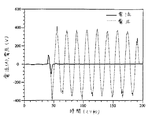
図8は、電流制限装置に振幅約370Vで60HzのAC電圧パルスを約150ミリ秒の間印加したときの、電流および電圧波形を示す。ACパルスを閉成移相角約120°で約40ミリ秒の間印加した。なお、電流は約+100Aの値まで増加し、ついで減少し、電圧が0Vを横切る際に0Aを横切り、次いで約−100Aの値まで(絶対値として)増加した。この後、電圧の絶対値は上昇し続けたにもかかわらず、電流の絶対値は、電流制限装置の作用により約2A未満のレベルに下がった。ついで、約195ミリ秒の間、AC電圧を+370Vと−370Vとの間で振動させ続けたとき、電流の絶対値は約2A未満のレベルに留まった。その後、この電圧パルスを停止した。したがって、電流制限装置は185Ωより大きい抵抗値の高抵抗状態を達成した。
【0028】
このように電流制限が実際に示された後、この電流制限装置が低電流(<30A)条件下で初期の低抵抗値0.1Ωに回復したことが実証された。この電流制限装置が再使用可能な電流制限装置として機能し得ることを証明するために、この試験順序を同じ370VのAC電圧パルスでもう一度繰り返したところ、成功した。
【0029】
本発明の電流制限装置は、(フューズとは異なり)2度以上機能すること、接触抵抗に基づく界面での加熱により動作開始すること、有機バインダのような低い熱分解/分解/アブレーション温度(<800°C)のバインダと導電性充填材を必要とすること、金属および/または半導体電極と圧力下で組み合わせられること、材料がPTCR効果を呈することを必要としないこと、ACおよびDC電圧/電流波形を制限する作用を有すること、500Vまでの電圧について試験されていること(上限は現在のところ不明)、電極を材料に一体的に取り付けるか簡単に圧力接触(圧接)できることが、当業者に明らかである。
【0030】
以下の実施例で、実際に行った実験を報告する。これらの実施例は、種々のバインダ材料、導電性充填材料、必要に応じて第3相充填材料および電極材料を使用し、シミュレーションの短絡電流を前述したのと同様の態様で制限した点ですべて有効であった。以下の実験はすべて、図1の基本的な電流制限装置形状を用いて行った。しかしながら、本発明は、図1に示す単一の複合材料と2電極の組合せに限定されず、複数の複合材料と3つ以上の電極の組合せを包含する。
【0031】
[実施例3]
導電性充填材として金属、具体的には銀を含有した、熱硬化性バインダ、具体的にはエポキシバインダを、次のように、アメス・ゴールドスミス社(AmesGoldsmith Corp.)から市販されている銀粒子であるAg4300(5.6g)、Ag1036(4.2g)およびAg1024(4.2g)と、ポキシ・テクノロジイ社(Epoxy−Technology Inc.)から商品名エポテック301(Epotek 301)として市販されている2成分エポキシを用いて用意した。エポキシ樹脂(2.3g)を硬化剤(0.6g)と混合し、ついで銀粒子を加え、混合物をテフロン(Teflon:登録商標)のモールド内に配置し、60°Cで1時間硬化した。Ni被覆Cuで電極を形成した。
【0032】
[実施例4]
導電性充填材として金属、具体的には銀を含有した、熱硬化性バインダ、具体的にはエポキシバインダを、ナショナル・スターチ・アンド・ケミカル社(National Starch and Chemical Company)のエイブルスティック・エレクトロニック・マテリアルズ・アンド・アドヘシブズ事業部(Ablestik Electronic Materials & Adhesives)から商品名エイブルボンド(Ablebond)967−1として市販されているの導電性接着材料を用いて用意した。混合物をテフロンのモールドに入れて、80°Cで2時間硬化した。Ni被覆Cuで電極を形成した。
【0033】
[実施例5]
導電性充填材として金属、具体的にはニッケルを含有した、熱硬化性バインダ、具体的にはエポキシバインダを、エポキシ・テクノロジイ社(Epoxy−Technology Inc.)から商品名エポテック(Epotek)N30として市販されている導電性接着材料を用いて用意した。混合物をテフロンのモールドに入れて、150°Cで約1時間硬化した。この特定の導電性複合材料用い、且つそれぞれ別々のNi被覆Cu、ステンレス鋼、Ag被覆CuおよびCu製の電極を有する電流制限装置を試験した。
【0034】
[実施例6]
導電性充填材として2成分金属導電充填材、具体的には銀とアルミニウムを含有した、エラストマバインダ、具体的にはシリコーンバインダを、2成分AおよびBを混合することにより製造した。成分Aは、末端ジメチルビニルシロキシ単位とジメチルシロキシ単位を有し、粘度が400cpsであるビニルシリコーンオルガノポリシロキサン流体(23g)と、アルミニウム粉末(37.3g)と、アメス・ゴールドスミス社から市販の銀粒子であるAg4300(46.6g)、Ag1036(37.3g)およびAg1024(37.3g)と、珪素に結合した化学結合水素約0.8重量%を有する流体を与えるように末端トリメチルシロキシ単位を有するシリコーンハイドライドシロキサン流体(1g)とから構成した。成分Bは、末端ジメチルビニルシロキシ単位とジメチルシロキシ単位を有し、粘度が400cpsであるビニルシリコーンオルガノポリシロキサン流体(2g)と、ジメチルマレエート(14μl)と、カーステッド(Karstedt)白金触媒(前掲、白金の5%キシレン溶液として83μl)とから構成した。成分A(40g)と成分B(0.44g)を混合し、モールドに注入した後、カーバー(Carver)プレスで約150°C、圧力約5000ポンドにて約30分間硬化させた。この例では、電極をNi被覆Cuまたはn型Si半導体で形成した。
【0035】
[実施例7]
導電性充填材として金属、具体的には銀のみを含有した、エラストマバインダ、具体的にはシリコーンバインダを、2成分AおよびBを混合することにより製造した。成分Aは、末端ジメチルビニルシロキシ単位とジメチルシロキシ単位を有し、粘度が400cpsであるビニルシリコーンオルガノポリシロキサン流体(23g)と、アメス・ゴールドスミス社から市販の銀粒子であるAg4300(46.6g)、Ag1036(37.3g)およびAg1024(37.3g)と、珪素に結合した化学結合水素約0.8重量%を有する流体を与えるように末端トリメチルシロキシ単位を有するシリコーンハイドライドシロキサン流体(1g)とから構成した。成分Bは、末端ジメチルビニルシロキシ単位とジメチルシロキシ単位を有し、粘度が400cpsであるビニルシリコーンオルガノポリシロキサン流体(2g)と、ジメチルマレエート(14μl)と、カーステッド白金触媒(前掲、白金の5%キシレン溶液として83μl)とから構成した。成分A(40g)と成分B(0.44g)を混合し、モールドに注入した後、カーバープレスで150°C、圧力5000ポンドにて30分間硬化させた。この例では、電極をNi被覆Cuで形成した。
【0036】
[実施例8]
エラストマバインダ、具体的には銀充填硬化性シリコーンを、2成分AおよびBを混合することにより製造した。成分Aは、末端ジメチルビニルシロキシ単位とジメチルシロキシ単位を有し、粘度が400cpsであるビニルシリコーンオルガノポリシロキサン流体(33g)と、アメス・ゴールドスミス社から市販の銀粒子であるAg4300(46.6g)、Ag1036(37.3g)およびAg1024(37.3g)と、ミヌシル(Minusil)のα−石英(23g)と、珪素に結合した化学結合水素約0.8重量%を有する流体を与えるように末端トリメチルシロキシ単位を有するシリコーンハイドライドシロキサン流体(2g)とから構成した。成分Bは、末端ジメチルビニルシロキシ単位とジメチルシロキシ単位を有し、粘度が400cpsであるビニルシリコーンオルガノポリシロキサン流体(10g)と、ジメチルマレエート(70μl)と、カーステッド白金触媒(前掲、白金の5%キシレン溶液として415μl)とから構成した。成分A(40g)と成分B(0.5g)を混合し、モールドに注入した後、カーバープレスで約150°C、圧力約5000ポンドにて約30分間硬化させた。この例では、電極をNi被覆Cuで形成した。
【0037】
[実施例9]
導電性充填材として2種の金属、具体的には銀とアルミニウムを含有した、強化エラストマバインダ、具体的にはフュームドシリカで補強した硬化性シリコーンを、2成分AおよびBから製造した。成分Aは、エラストマバインダ、すなわち末端ジメチルビニルシロキシ単位とジメチルシロキシ単位を有し、粘度が400cpsであるビニルシリコーンオルガノポリシロキサン流体(23g)と、珪素に結合した化学結合水素約0.8重量%を有する流体を与えるように末端トリメチルシロキシ単位を有するシリコーンハイドライドシロキサン流体(2g)と、シクロオクタメチルテトラシロキサンおよびヘキサメチルジシラザンで処理した比表面積300m2 /gの二重処理フュームドシリカ(1.2g)と、アルミニウム粉末(37.3g)と、アメス・ゴールドスミス社から市販の銀粒子であるAg4300(46.6g)、Ag1036(37.3g)およびAg1024(37.3g)とから構成した。成分Bは、末端ジメチルビニルシロキシ単位とジメチルシロキシ単位を有し、粘度が400cpsであるビニルシリコーンオルガノポリシロキサン流体(2g)と、ジメチルマレエート(14μl)と、カーステッド白金触媒(前掲、83μl)とから構成した。成分A(40g)と成分B(0.44g)を合わせ、手で混合して硬化性組成物を得、これをモールドに入れた。カーバープレスで150°C、圧力5000ポンドにて30分間硬化させた。この例では、電極をNi被覆Cuで形成した。
【0038】
[実施例10]
エラストマバインダ、具体的にはニッケル充填シリコーンを、2成分AおよびBから製造した。成分Aは、末端ジメチルビニルシロキシ単位とジメチルシロキシ単位を有し、粘度が400cpsであるビニルシリコーンオルガノポリシロキサン流体(25g)と、INCOタイプ123のニッケル粉末(100g)と、珪素に結合した化学結合水素約0.8重量%を有する流体を与えるように末端トリメチルシロキシ単位を有するシリコーンハイドライドシロキサン流体(2g)とから構成した。成分Bは、末端ジメチルビニルシロキシ単位とジメチルシロキシ単位を有し、粘度が400cpsであるビニルシリコーンオルガノポリシロキサン流体(10g)と、ジメチルマレエート(70μl)と、カーステッド白金触媒(白金の5%キシレン溶液として415μl)とから構成した。成分A(40g)と成分B(0.5g)を混合し、モールドに注入した後、カーバープレスで150°C、圧力5000ポンドにて30分間硬化させた。この例では、電極をNi被覆Cuで形成した。
【0039】
[実施例11]
半導電性充填材、具体的にはカーボンブラックを含有する熱可塑性バインダ、具体的にはポリテトラフルオロエチレンバインダの市販品を入手した。すなわちダブリュ・エル・ゴア・アンド・アソシエイツ社(W. L. Gore & Associates, Inc.)から商品名GS−2100−080−5000−SCとして市販の導電性フッ素ポリマーを、Ni被覆Cuの電極とともに使用した。
[実施例12]
さらに、導電性充填材として金属、具体的には銀を含有した、熱可塑性バインダ、具体的にはポリ(エチレングリコール)を製造した。アメス・ゴールドスミス社から市販の銀粒子であるAg4300(2.8g)、Ag1036(2.1g)およびAg1024(2.1g)からなる銀粒子混合物を約80°Cに加熱し、約80°Cの溶融ポリ(エチレングリコール)(MW8000)に加え、混合した。この材料をテフロンのモールドに注入し、室温で硬化させた。この例では電極をNi被覆Cuから形成した。
【0040】
上述した実施例について、電流制限装置として試験する場合、電極を導電性複合材料に対して約6乃至約370psiの範囲の圧力でプレスした。具体的には、実施例3、4、6、7および11では約170psiの圧力を用い、実施例5、8および10では約370psiの圧力を、実施例9および12では約6psiの圧力を用いた。上記圧力範囲を実際にテストしたが、本発明の装置はそれより高い圧力でも低い圧力でも適正な性能を示す可能性がある。
【0041】
上述したところから明らかなように、低い熱分解温度または蒸発温度(<800°C)を有するバインダ材料、たとえば熱可塑性樹脂(たとえばポリテトラフルオロエチレン、ポリ(エチレングリコール)、ポリエチレン、ポリカーボネート、ポリイミド、ポリアミド、ポリメチルメタクリレート、ポリエステルなど);熱硬化性樹脂(たとえばエポキシ、ポリエステル、ポリウレタン、フェノール、アルキッドなど);エラストマ(たとえばシリコーン(ポリオルガノシロキサン)、ポリウレタン、イソプレンゴム、ネオプレンなど);有機または無機結晶を、粒子または発泡体形態の導電性充填材、たとえば金属(たとえばニッケル、銀、銅など)または半導体(たとえばカーボンブラック、二酸化チタンなど)と組合せ、金属または半導体電極をその導電性複合材料に圧接したものも、本発明の電流制限装置として有効な性能を発揮する。
【0042】
複合材料の特性、たとえば機械的特性や誘電特性を向上させるために、あるいは消弧特性や難燃性を与えるために、第3相充填材を使用することができる。複合材料に第3相充填材として使用することのできる材料としては、フュームドシリカなどの補強用充填材や、沈降シリカなどの増量用充填材から選ばれる充填材、またはこれらの混合物がある。他の充填材として、二酸化チタン、リトポン、酸化亜鉛、珪藻珪酸塩、シリカエーロゲル、酸化鉄、珪藻土、炭酸カルシウム、シラザン処理シリカ、シリコーン処理シリカ、ガラス繊維、酸化マグネシウム、酸化クロム、酸化ジルコニウム、α−石英、焼成クレー、炭素、グラファイト、コルク、綿、重炭酸ナトリウム、ほう酸、アルミナ水和物などがある。他の添加剤としては、電流制限装置へのダメージ、たとえば突然の衝撃による亀裂発生を防止する耐衝撃性向上剤、電流制限装置における火炎形成を防止および/または阻止する難燃剤、ユーザの要求に応えて特定の色成分を与える染料および着色剤、日光その他の紫外線にさらされることによる物理的特性の低下を防止するUV遮断剤などが上げられる。
【0043】
最後に、本発明の限流器は並列な線形または非線形回路素子、たとえば抵抗器またはバリスタとともに用いることができる。
本明細書やここに開示した発明の実施態様を参照すれば、本発明の他の実施態様も当業者には明らかである。以上の説明も実施例も本発明の例示にすぎず、本発明の範囲は特許請求の範囲に記載の通りである。
【図面の簡単な説明】
【図1】本発明による電流制限装置の概略構成図である。
【図2】短絡条件のシミュレーションに用いる電圧パルスを示すグラフである。
【図3】図2に示すような電圧パルスを図1の電流制限装置に印加したときの、電流制限装置に流れる電流および電流制限装置両端間の電圧を示すグラフである。
【図4】シミュレーションにより短絡した電流制限装置の電流および電圧の初期部分を示すグラフである。
【図5】図1の電流制限装置の抵抗を時間の関数として示すグラフである。
【図6】ニッケル充填エポキシ材料を導電性複合材料として用いて製造した図1の電流制限装置について、短絡条件をシミュレーションした約500ボルトの電圧パルスを印加したときの、電流制限装置に流れる電流と電流制限装置両端間の電圧を示すグラフである。
【図7】電圧波形を電流波形で割ることにより図6のデータから得られる図1の電流制限装置の抵抗を示すグラフである。
【図8】振幅約370V、60HzのAC電圧パルスを150ミリ秒の間、図1の電流制限装置に印加したときの電流および電圧波形を示すグラフである。[0001]
[Industrial application fields]
The present invention relates generally to devices suitable for general circuit protection, such as power distribution and motor control applications, and in particular, simple, reusable, and low cost that can be manufactured for various applications. Relates to the device. More specifically, the present invention relates to a current limiting device using a conductive composite material and a heterogeneous resistance distribution structure, which is suitable for a relatively high power application having a system voltage of 100 V or more and a short-circuit current of 100 A or more.
[0002]
[Prior art]
There are many devices that can limit the current flowing in a circuit when a short circuit occurs. Some current limiting devices currently in use include filled polymeric materials that have an effect commonly referred to as PTCR (Positive Resistance Temperature Coefficient) or PTC effect. As a characteristic of the PTCR or PTC effect, at certain switch temperatures, the PTCR material undergoes a transformation from relatively conductive to relatively resistive. Some conventional current limiting devices have a PTCR material (typically carbon black filled polyethylene) disposed between the pressure contact electrodes.
[0003]
In use, such conventional current limiting devices are placed in the circuit to be protected. Under normal circuit conditions, the current limiting device is in a highly conductive state. When a short circuit occurs, the PTCR material generates heat due to resistance heating and eventually the temperature exceeds the switch temperature. At this point, the resistance of the PTCR material changes to a high resistance state, limiting the short circuit current. When the short circuit condition disappears, the current limiting device cools below the switch temperature and returns to the highly conductive state. The current limiting device in the highly conductive state can switch back to the high resistance state again in response to a future short circuit occurrence.
[0004]
U.S. Pat. No. 5,382,938 is disposed in contact with a body of a conductive polymer composition having a positive temperature coefficient resistivity and two parallel end faces of the body for current flow through the body. A PTC device comprising two electrodes is described. The polymer composition of the main body is obtained by distributing a conductive powder material in a polymer material. The term “PTC element” is recognized as a term for an element that exhibits a positive temperature coefficient of resistance at switch temperature, as shown in FIG. 1 of US Pat. No. 5,382,938. At least one of the parallel surfaces of the body is in free contact with the electrode or with the parallel surface of another body of the conductive polymer composition. A pressure device applies pressure against the electrodes in a direction perpendicular to the parallel surface of the body (s). The pressure device is preferably provided with a pressure application device having elastic ability. Since the PTC element changes from the low resistance state to the high resistance state and then returns to the initial resistance, it can be reused even after receiving a short-circuit current. The parallel surfaces of the polymer composition body (s) should be concentric. The PTC element is used in an electric circuit for the purpose of overcurrent protection.
[0005]
US Pat. No. 5,313,184 describes an electrical resistor having a resistor body disposed between two contact terminals. The resistor core includes an element that exhibits PTC behavior, which forms a conductive path between two contact terminals below a temperature characteristic of the material. Resistors can be simple and inexpensive, but still have a highly rated current carrying capacity that is protected against local and global overvoltages. This is accomplished by adding additional material that exhibits varistor behavior to the resistor core. The varistor material is connected in parallel with at least one subsection of the conductive path to form at least one varistor and is in electrical contact with the portion of the PTC material that forms the at least one subsection. . The parallel connection of the element having the PTC behavior and the varistor can be realized by both a micro structure and a macro arrangement.
[0006]
European Patent 0,640,995A1 describes an electrical resistance element which includes a resistance material having a PTC characteristic and which is arranged between two parallel planar electrodes and applies pressure to both electrodes. The resistance material is configured by embedding two kinds of filling components made of conductive particles in a polymer base material. When a short-circuit current occurs, in the surface layer that is in contact with the electrode and contains at least the first filling component of the two filling components, the resistivity of the resistive material is stepped or stepped when the temperature is higher than the limit temperature value. Change. A PTC characteristic in which a composite material containing at least a polymer matrix and a second filling component has a step-like change characteristic that is at least one digit larger than the surface layer by appropriately selecting the second filling component of the two kinds of filling components As shown. At the same time, the resistivity of this composite material is an order of magnitude lower than that of the composite material formed from the polymer matrix and the first filler component.
[0007]
All of the above-mentioned measures are based on PTC behavior and seek to obtain a simpler and more durable current limiter, but are suitable for general circuit protection in power distribution and motor control applications, There remains a need for a simpler, more durable, reusable, low cost current limiting device that can be tailored to the application. Such a device protects the circuit from at least two shorts, preferably multiple shorts, does not require the material to exhibit a PTCR effect, and at a high voltage of 100-500 volts or higher. It is required to be usable.
[0008]
SUMMARY OF THE INVENTION
Current limiting devices are used in many applications to protect sensitive components in electrical circuits from large fault currents. Applications range from low voltage / current circuits to high voltage / current distribution systems. The present invention provides a simple, reusable, low cost current limiting device that can be fabricated for a variety of applications.
[0009]
According to the present invention, a conductive composite material containing a conductive filler having no PTC effect, at least two electrodes operatively disposed with respect to the composite material, and operatively between the outer electrodes. A current limiting device is provided comprising an inhomogeneous resistance distribution disposed and means for applying a compressive pressure to the conductive composite material.
Accordingly, an object of the present invention is to provide a current limiting device made of a material that does not exhibit any PTC effect.
[0010]
Other objects and advantages of the present invention will become apparent from the following detailed description with reference to the drawings.
[0011]
【detailed explanation】
The current limiting device of the present invention uses a composite material including a binder having a low pyrolysis temperature or low evaporation temperature and a conductive filler in combination with a heterogeneous resistance distribution structure. The binder should be selected such that significant gas evolution occurs at low temperatures (<800 ° C.). The heterogeneous resistance distribution structure is typically chosen such that at least one thin layer of the current limiting device has a much higher resistance than the rest of the current limiting device.
[0012]
While not intending to be bound by theory, the superior effect of the present invention is that when a short circuit occurs, this thin layer of adiabatic resistance heating is followed by rapid thermal expansion and from the binder material. It is believed that the generation of gas results in partial or complete physical separation of the current limiting device at the thin layer, resulting in a greater overall resistance of the device to the current. . Thus, the current limiting device limits the current flowing in the short circuit current path. When the short circuit is removed by the external means, the current limiting device returns to the low resistance state due to the compression pressure incorporated in the current limiting device, and the current can flow normally. The current limiting device of the present invention can be reused many times for such short circuit conditions, depending on factors such as the severity and length of each short circuit.
[0013]
In order to further clarify the present invention, preferred embodiments and examples will be described below, but these examples are merely examples of the use of the present invention. According to one embodiment of the present invention, the current limiting device is configured using a conductive composite material so that a non-uniform resistance distribution is generated throughout the device. In order for this device to work properly as a reusable current limiting device, at least one thin layer of the current limiting device is required. The Located perpendicular to the direction of current flow so that it has a resistance much greater than the average resistance of an average layer of the same dimensions and orientation in the device do it , Non-uniform resistance distribution Formation Must. Furthermore, the current limiting device must apply a compressive pressure in a direction perpendicular to the chosen high resistance thin layer.
[0014]
In one example of a current limiting device according to the present invention, a highly conductive composite material having a binder with a low pyrolysis temperature and a conductive filler is pressed against the electrode, and significant between the composite material and the electrode (one or both). Make sure there is proper contact resistance. In use, the current limiting device is placed in series with the electrical circuit to be protected. During normal operation, the resistance of the current limiting device is low (in this example, the resistance of the current limiting device is equal to the sum of the resistance of the highly conductive composite, the resistance of the electrode and the contact resistance). When a short circuit occurs, a high current density current begins to flow through the device. At the initial stage of the short circuit, the resistance heating of the device is considered adiabatic. Thus, the selected thin layer with the higher resistance of the current limiter is believed to generate heat much faster than the rest of the current limiter. If the thin layer is properly designed, the thin layer will generate heat quickly enough, and thermal expansion of the thin layer and / or gas generation from the thin layer will cause separation in the current limiting device at the thin layer. it is conceivable that.
[0015]
In a typical current limiting device, it is believed that the electrode leaves the composite material due to the evaporation and / or ablation of the composite material. In this separated state, ablation of the composite material occurs, and it is considered that an arc is generated between the separated layers of the current limiting device. However, the total resistance in the isolated state is much greater than the resistance in the non-isolated state. This large arc resistance is thought to be due to the combination of the high pressure generated at the interface due to gas generation from the binder of the composite material and the deionization characteristics of the gas. In any case, the current limiting device of the present invention is effective in limiting the short circuit current so that other components of the circuit are not destroyed by the short circuit.
[0016]
After interrupting the short circuit current, the current limiting device of the present invention, if properly designed, will return to a non-separated state, i.e., recover, because the compression pressure acts to press the separated layers together. . Once multiple layers of the current limiting device return to a non-isolated state, i.e., a low resistance state, the current limiting device is fully ready to perform current limiting action in response to other shorted conductors in the future. Is in a state.
[0017]
Another embodiment of the current limiter of the present invention uses a parallel current path that includes resistors, varistors or other linear or non-linear elements to maximize the maximum that can appear across the current limiter in a particular circuit. It can be configured to control the voltage or to form another path through a portion of the circuit energy to extend the useful life of the current limiting device.
[0018]
[Example 1]
In order to demonstrate the effect of the present invention, a current limiting device as shown in FIG. 1 was produced. The conductive composite material was composed of an elastomer as a binder material, such as a silicone elastomer, and a metal as a filler, such as silver, and the resistivity was about 0.004 Ω-cm. A silver filled curable silicone material (elastomer) was prepared by mixing the two components A and B. Component A is a vinyl silicone organopolysiloxane fluid (23 g) having terminal dimethylvinylsiloxy units and dimethylsiloxy units and a viscosity of 400 cps at 25 ° C. and commercially available from Ames Goldsmith Corp. Silver particles, Ag4300 (46.6 g), Ag1036 (37.3 g), and Ag1024 (37.3 g), and a fluid having about 0.8% by weight of chemically bonded hydrogen bonded to silicon. And a silicone hydride siloxane fluid (1 g) having trimethylsiloxy units. Component B consists of a vinyl silicone organopolysiloxane fluid (2 g) having terminal dimethylvinylsiloxy units and dimethylsiloxy units and a viscosity of 400 cps, dimethyl maleate (14 μl), and a Karstedt platinum catalyst (platinum). (83 μl as a 5% xylene solution) (for details, see US Pat. No. 3,775,452). Component A (40 g) and Component B (0.44 g) were mixed and poured into a mold and then cured for 30 minutes at 150 ° C. and 5000 pounds pressure with a Carver press.
[0019]
The electrode was made from nickel electroplated copper and pressed into the composite material. Note that neither the conductive composite material nor the electrode material exhibits a PTCR switching effect. The electrode was about 1/4 inch in diameter. These electrodes were placed in the center of a composite material 3/4 inch in diameter and about 1/8 inch thick. Pressure was applied by applying a force of about 3.7 kg between both electrodes (pressure was about 170 psi). The current limiting device of this example functioned as a simple resistor having a resistance value of about 0.06Ω when a current of less than about 30 A was passed through the device.
[0020]
FIG. 2 shows voltage pulses used in the simulation of the short circuit condition. The voltage is about 2.5V to simulate normal circuit operation for the first about 1 millisecond. The voltage then jumps to about 100V for about 3 milliseconds for simulation of short circuit conditions. The voltage then drops to about 2.5V in about 4 milliseconds for simulation of short circuit correction.
[0021]
FIG. 3 shows the current that flows through the current limiting device and the voltage that appears across the device when the voltage pulse shown in FIG. 2 is applied to the current limiting device.
FIG. 4 is an enlarged view of an initial part of the short-circuit simulation of FIG. When the voltage jumps to about 100V, the current jumps to about 190A, then suddenly drops to a low value of about 1A, and then remains at that value for the remainder of the pulse. Therefore, the current is limited to a value of 1A or less from the predicted value of about 1667A (100V / 0.06Ω).
[0022]
FIG. 5 is a graph showing the resistance of the current limiting device as a function of time. It can be seen that the resistance changes more than 3000 times when a pulse of about 100V is applied to the sample current limiter. At the end of this pulse test, the resistance of the current limiter returned to an initial value of about 0.06Ω (measured using a 30 A current probe). Thus, the current limiting device is ready to wait for the next current limiting operation. In fact, when this current limiting device was further subjected to a current limiting operation three times, no kind of failure occurred. There is no reason to believe that this current limiter will not work more often because the degree of damage to both the material and the electrode was low.
[0023]
[Example 2]
The operating characteristics of another example of a current limiting device constructed in accordance with the present invention using a suitable conductive composite material are shown in FIGS. In this example, the current limiting device structure shown in FIG. 1 is used, and the composite material is a thermosetting binder, such as an epoxy binder marketed under the trade name N30 from Epoxy-Technology Inc. And a metal as a conductive filler, for example, nickel powder. This composite material has a resistivity of about 0.02 to 0.03 Ω-cm and does not exhibit a PTCR effect. Physically, the apparatus of this example uses nickel electroplated copper electrodes with a diameter of about 1/4 inch and these are placed in the center of a composite material with a diameter of 3/4 inch and a thickness of about 1/8 inch. . Pressure was applied by applying a force of about 8.2 kg between both electrodes (pressure was about 370 psi). The current limiting device of this example functioned as a simple resistor having a resistance value of about 0.1Ω when a current of less than about 30 A was passed through the device.
[0024]
FIG. 6 shows the current flowing through the current limiting device and the voltage appearing across the device when a voltage pulse of about 500 V is applied to the current limiting device to simulate the short-circuit condition. At the beginning of the applied voltage pulse at 0 seconds, the current rises to about 200 A and then maintains that value for about 1.2 milliseconds. This initial current value of about 200 A was limited by the output capability of the voltage pulse device used in this test. Due to the limitations of this device, the voltage does not reach 500V during this initial 1.2 milliseconds. However, during this initial 1.2 milliseconds, the voltage of the current limiting device increases as the current limiting device transitions to a high resistance state. After 1.2 milliseconds, the current limiting device reached a high resistance state, so that the current decreased to a value lower than about 50 A due to the action of the current limiting device, and the measured voltage across the current limiting device was up to 500V. The current remained at a level below about 50 A until the device voltage was turned off after 14 milliseconds.
[0025]
FIG. 7 shows the resistance of the current limiting device obtained from the data shown in FIG. 6 by dividing the voltage waveform by the current waveform. It should be noted that at the start of the voltage pulse, the resistance is about 0.1Ω, the resistance rises to a value higher than about 10Ω after about 1.2 milliseconds, and this high resistance state until the voltage pulse stops at 14 milliseconds. Maintained. After actually showing current limiting in this way, it was demonstrated that the current limiting device recovered to an initial low resistance value of 0.1Ω under low current (<30 A) conditions. In order to prove that this current limiter can function as a reusable current limiter, this test sequence was repeated on the same device and a total of three operations with 500 V short circuit simulation voltage pulses were successful.
[0026]
The embodiments shown in FIGS. 3-7 demonstrate that the current limiting device of the present invention can effectively limit the current in the event of a short circuit in a direct current (DC) circuit without the use of a material having a PTCR effect. .
FIG. 8 shows that the current limiting device of the present invention can also be used as a reusable current limiting device for alternating current (AC) circuits. The current limiting device used in the experiment shown in FIG. 8 is the same as the device used in the previous embodiment for a direct current (DC) circuit, both in material and configuration. The initial resistance of the current limiting device, measured using a low current (<30 A) pulse, was about 0.1Ω.
[0027]
FIG. 8 shows current and voltage waveforms when a 60 Hz AC voltage pulse with an amplitude of about 370 V is applied to the current limiter for about 150 milliseconds. AC pulses were applied for about 40 milliseconds at a closed phase shift angle of about 120 °. Note that the current increased to a value of about +100 A, then decreased, crossed 0 A when the voltage crossed 0 V, and then increased (as an absolute value) to a value of about −100 A. After this, although the absolute value of the voltage continued to rise, the absolute value of the current decreased to a level of less than about 2 A due to the action of the current limiting device. Then, when the AC voltage was kept oscillating between + 370V and -370V for about 195 milliseconds, the absolute value of the current remained at a level of less than about 2A. Thereafter, this voltage pulse was stopped. Therefore, the current limiting device achieved a high resistance state with a resistance value greater than 185Ω.
[0028]
After actually showing current limiting in this way, it was demonstrated that the current limiting device recovered to an initial low resistance value of 0.1Ω under low current (<30 A) conditions. To prove that this current limiter can function as a reusable current limiter, this test sequence was repeated once more with the same 370V AC voltage pulse and was successful.
[0029]
The current limiting device of the present invention functions more than twice (unlike a fuse), starts operating by heating at the interface based on contact resistance, low pyrolysis / decomposition / ablation temperature (< 800 ° C.) binder and conductive filler, combined with metal and / or semiconductor electrodes under pressure, material does not need to exhibit a PTCR effect, AC and DC voltage / current Those skilled in the art have the ability to limit the waveform, have been tested for voltages up to 500V (the upper limit is currently unknown), and that the electrodes can be either integrally attached to the material or easily pressure contacted (pressure welding) it is obvious.
[0030]
In the following examples, actual experiments performed are reported. These examples all use various binder materials, conductive filler materials, optionally third phase filler materials and electrode materials, and limit the short circuit current in the simulation in the same manner as described above. It was effective. All the following experiments were performed using the basic current limiter configuration of FIG. However, the present invention is not limited to the combination of a single composite material and two electrodes shown in FIG. 1, but includes a combination of a plurality of composite materials and three or more electrodes.
[0031]
[Example 3]
A silver, commercially available from Ames Goldsmith Corp., containing a metal, specifically silver, as a conductive filler, specifically a thermosetting binder, specifically an epoxy binder, as follows: Particles Ag4300 (5.6 g), Ag1036 (4.2 g) and Ag1024 (4.2 g) and commercially available from Epoxy-Technology Inc. under the trade name Epotek 301 Prepared using two-component epoxy. Epoxy resin (2.3 g) was mixed with a curing agent (0.6 g), then silver particles were added and the mixture was placed in a Teflon mold and cured at 60 ° C. for 1 hour. An electrode was formed of Ni-coated Cu.
[0032]
[Example 4]
A thermosetting binder, specifically an epoxy binder, containing a metal, specifically silver, as a conductive filler, is available from National Starch and Chemical Company, Able Stick Electronic Company. It was prepared using a conductive adhesive material commercially available under the trade name Ablebond 967-1 from the Materials and Adhesives Division (Ablestik Electronic Materials & Adhesives). The mixture was placed in a Teflon mold and cured at 80 ° C. for 2 hours. An electrode was formed of Ni-coated Cu.
[0033]
[Example 5]
A thermosetting binder, specifically an epoxy binder, containing a metal, specifically nickel, as the conductive filler is traded from Epoxy-Technology Inc. under the trade name Epotek N30. A commercially available conductive adhesive material was used. The mixture was placed in a Teflon mold and cured at 150 ° C. for about 1 hour. A current limiting device using this specific conductive composite and having separate Ni coated Cu, stainless steel, Ag coated Cu and Cu electrodes was tested.
[0034]
[Example 6]
A two-component metal conductive filler, specifically an elastomer binder, specifically a silicone binder, containing silver and aluminum as a conductive filler was prepared by mixing two components A and B. Component A consists of vinyl silicone organopolysiloxane fluid (23 g) having terminal dimethylvinylsiloxy units and dimethylsiloxy units and a viscosity of 400 cps, aluminum powder (37.3 g), and commercially available from Ames Goldsmith. Terminal trimethylsiloxy units to give a fluid having silver particles Ag4300 (46.6 g), Ag1036 (37.3 g) and Ag1024 (37.3 g) and about 0.8 wt% chemically bonded hydrogen bonded to silicon. And a silicone hydride siloxane fluid (1 g). Component B consists of a vinylsilicone organopolysiloxane fluid (2 g) having terminal dimethylvinylsiloxy units and dimethylsiloxy units and a viscosity of 400 cps, dimethyl maleate (14 μl), a Karstedt platinum catalyst (see above). And 83 μl of a 5% xylene solution of platinum). Component A (40 g) and Component B (0.44 g) were mixed and poured into a mold and then cured in a Carver press at about 150 ° C. and a pressure of about 5000 pounds for about 30 minutes. In this example, the electrode was formed of Ni-coated Cu or n-type Si semiconductor.
[0035]
[Example 7]
An elastomer binder, specifically a silicone binder, containing only metal, specifically silver, as the conductive filler was prepared by mixing the two components A and B. Component A consists of a vinylsilicone organopolysiloxane fluid (23 g) having terminal dimethylvinylsiloxy units and dimethylsiloxy units and a viscosity of 400 cps, and Ag4300 (46.6 g), a silver particle commercially available from Ames Goldsmith. ), Ag1036 (37.3 g) and Ag1024 (37.3 g), and a silicone hydride siloxane fluid having terminal trimethylsiloxy units (1 g) to give a fluid having about 0.8 wt% chemically bonded hydrogen bonded to silicon. And consisted of Component B consists of a vinyl silicone organopolysiloxane fluid (2 g) having terminal dimethylvinylsiloxy units and dimethylsiloxy units and having a viscosity of 400 cps, dimethyl maleate (14 μl), a casted platinum catalyst (see above, platinum 83% as a 5% xylene solution). Component A (40 g) and Component B (0.44 g) were mixed, poured into a mold, and cured with a carver press at 150 ° C. and a pressure of 5000 pounds for 30 minutes. In this example, the electrode was formed of Ni-coated Cu.
[0036]
[Example 8]
An elastomer binder, specifically silver filled curable silicone, was prepared by mixing the two components A and B. Component A consists of a vinyl silicone organopolysiloxane fluid (33 g) having terminal dimethylvinylsiloxy units and dimethylsiloxy units and a viscosity of 400 cps, and Ag4300 (46.6 g), a silver particle commercially available from Ames Goldsmith. ), Ag1036 (37.3 g) and Ag1024 (37.3 g), Minusil α-quartz (23 g), and a fluid having about 0.8 wt% of chemically bonded hydrogen bonded to silicon. And composed of a silicone hydride siloxane fluid (2 g) with terminal trimethylsiloxy units. Component B consists of a vinyl silicone organopolysiloxane fluid (10 g) having terminal dimethylvinylsiloxy units and dimethylsiloxy units and a viscosity of 400 cps, dimethyl maleate (70 μl), a casted platinum catalyst (see above, platinum 415 μl) as a 5% xylene solution. Component A (40 g) and Component B (0.5 g) were mixed and poured into a mold and then cured with a carver press at about 150 ° C. and a pressure of about 5000 pounds for about 30 minutes. In this example, the electrode was formed of Ni-coated Cu.
[0037]
[Example 9]
A curable silicone reinforced with a reinforced elastomer binder, specifically fumed silica, containing two metals as conductive fillers, specifically silver and aluminum, was prepared from two components A and B. Component A comprises an elastomer binder, a vinyl silicone organopolysiloxane fluid (23 g) having terminal dimethylvinylsiloxy units and dimethylsiloxy units and a viscosity of 400 cps, and about 0.8% by weight of chemically bonded hydrogen bonded to silicon. A specific surface area of 300 m treated with a silicone hydride siloxane fluid (2 g) having terminal trimethylsiloxy units and cyclooctamethyltetrasiloxane and hexamethyldisilazane to give a fluid having 2 / G double-treated fumed silica (1.2 g), aluminum powder (37.3 g), silver particles commercially available from Ames Goldsmith, Ag4300 (46.6 g), Ag1036 (37.3 g) And Ag1024 (37.3 g). Component B consists of a vinyl silicone organopolysiloxane fluid (2 g) having terminal dimethylvinylsiloxy units and dimethylsiloxy units and a viscosity of 400 cps, dimethyl maleate (14 μl), and a casted platinum catalyst (supra, 83 μl). And consisted of Component A (40 g) and Component B (0.44 g) were combined and mixed by hand to obtain a curable composition, which was placed in a mold. Cured with a carver press at 150 ° C. and a pressure of 5000 pounds for 30 minutes. In this example, the electrode was formed of Ni-coated Cu.
[0038]
[Example 10]
An elastomer binder, specifically nickel-filled silicone, was prepared from the two components A and B. Component A consists of a vinyl silicone organopolysiloxane fluid (25 g) having terminal dimethylvinylsiloxy units and dimethylsiloxy units and a viscosity of 400 cps, nickel powder of INCO type 123 (100 g), and silicon bonded chemical bond Consists of a silicone hydride siloxane fluid (2 g) with terminal trimethylsiloxy units to give a fluid having about 0.8 wt% hydrogen. Component B consists of a vinyl silicone organopolysiloxane fluid (10 g) having terminal dimethylvinylsiloxy units and dimethylsiloxy units and a viscosity of 400 cps, dimethyl maleate (70 μl), casted platinum catalyst (5% platinum) 415 μl) as a xylene solution. Component A (40 g) and Component B (0.5 g) were mixed and poured into a mold, and then cured with a carver press at 150 ° C. and a pressure of 5000 pounds for 30 minutes. In this example, the electrode was formed of Ni-coated Cu.
[0039]
[Example 11]
A commercially available product of a semiconductive filler, specifically a thermoplastic binder containing carbon black, specifically a polytetrafluoroethylene binder, was obtained. That is, a conductive fluoropolymer commercially available under the trade name GS-2100-080-5000-SC from W. L. Gore & Associates, Inc., together with an electrode of Ni-coated Cu. used.
[Example 12]
Furthermore, a thermoplastic binder, specifically poly (ethylene glycol), containing a metal, specifically silver, as a conductive filler was manufactured. A silver particle mixture consisting of Ag4300 (2.8 g), Ag1036 (2.1 g) and Ag1024 (2.1 g), commercially available silver particles from Ames Goldsmith, was heated to about 80 ° C. and about 80 ° C. Of molten poly (ethylene glycol) (MW 8000) and mixed. This material was poured into a Teflon mold and allowed to cure at room temperature. In this example, the electrode was formed from Ni-coated Cu.
[0040]
For the examples described above, when tested as a current limiting device, the electrodes were pressed against the conductive composite at a pressure in the range of about 6 to about 370 psi. Specifically, Examples 3, 4, 6, 7 and 11 use a pressure of about 170 psi, Examples 5, 8 and 10 use a pressure of about 370 psi, and Examples 9 and 12 use a pressure of about 6 psi. It was. Although the above pressure range was actually tested, the device of the present invention may show adequate performance at higher and lower pressures.
[0041]
As is apparent from the above, binder materials having a low pyrolysis temperature or evaporation temperature (<800 ° C.), such as thermoplastic resins (eg polytetrafluoroethylene, poly (ethylene glycol), polyethylene, polycarbonate, polyimide, Polyamide, polymethyl methacrylate, polyester, etc.); thermosetting resin (eg, epoxy, polyester, polyurethane, phenol, alkyd, etc.); elastomer (eg, silicone (polyorganosiloxane), polyurethane, isoprene rubber, neoprene, etc.); organic or inorganic The crystals are combined with conductive fillers in the form of particles or foams, such as metals (eg nickel, silver, copper etc.) or semiconductors (eg carbon black, titanium dioxide etc.), metal or semi That pressed against the body electrode in the conductive composite material also exhibits an effective performance as a current limiting device of the present invention.
[0042]
Third phase fillers can be used to improve composite properties, such as mechanical properties and dielectric properties, or to provide arc-extinguishing properties and flame retardancy. Materials that can be used as the third phase filler in the composite material include fillers selected from reinforcing fillers such as fumed silica, fillers for weight increase such as precipitated silica, or mixtures thereof. Other fillers include titanium dioxide, lithopone, zinc oxide, diatom silicate, silica aerogel, iron oxide, diatomaceous earth, calcium carbonate, silazane treated silica, silicone treated silica, glass fiber, magnesium oxide, chromium oxide, zirconium oxide, Examples include α-quartz, calcined clay, carbon, graphite, cork, cotton, sodium bicarbonate, boric acid, and alumina hydrate. Other additives include impact resistance improvers that prevent damage to the current limiting device, such as cracking due to sudden impacts, flame retardants that prevent and / or prevent flame formation in the current limiting device, to meet user requirements In response, there are dyes and colorants that give specific color components, UV blocking agents that prevent deterioration of physical properties due to exposure to sunlight and other ultraviolet rays, and the like.
[0043]
Finally, the current limiter of the present invention can be used with parallel linear or non-linear circuit elements such as resistors or varistors.
Other embodiments of the invention will be apparent to those skilled in the art from reference to the specification and embodiments of the invention disclosed herein. The above description and examples are merely illustrative of the present invention, and the scope of the present invention is as set forth in the appended claims.
[Brief description of the drawings]
FIG. 1 is a schematic configuration diagram of a current limiting device according to the present invention.
FIG. 2 is a graph showing voltage pulses used in a simulation of a short circuit condition.
3 is a graph showing the current flowing through the current limiting device and the voltage across the current limiting device when a voltage pulse as shown in FIG. 2 is applied to the current limiting device of FIG.
FIG. 4 is a graph showing an initial portion of current and voltage of a current limiting device short-circuited by simulation.
FIG. 5 is a graph showing resistance of the current limiting device of FIG. 1 as a function of time.
FIG. 6 shows the current flowing through the current limiting device when a voltage pulse of about 500 volts simulating a short circuit condition is applied to the current limiting device of FIG. 1 manufactured using a nickel-filled epoxy material as a conductive composite material. It is a graph which shows the voltage between both ends of a current limiting device.
7 is a graph showing the resistance of the current limiting device of FIG. 1 obtained from the data of FIG. 6 by dividing the voltage waveform by the current waveform.
8 is a graph showing current and voltage waveforms when an AC voltage pulse with an amplitude of about 370 V and 60 Hz is applied to the current limiting device of FIG. 1 for 150 milliseconds.
Claims (1)
前記少なくとも2つの電極の間に配置された導電性複合材料であって、該導電性複合材料は、(A)800℃以下で熱分解または蒸発し、ガスが発生するバインダと、(B)導電性充填材を含んでいる前記導電性複合材料と、
前記導電性複合材料に圧縮圧力を加える手段とを備え、
短絡発生時において、前記導電性複合材料における断熱抵抗加熱が前記バインダの急速な熱膨張と蒸発を起こさせ、前記少なくとも2つの電極と前記導電性複合材料の間で少なくとも部分的な物理的分離が生じる、電流制限装置。At least two electrodes;
A conductive composite material disposed between the at least two electrodes, the conductive composite material comprising: (A) a binder that thermally decomposes or evaporates at 800 ° C. or lower to generate gas; and (B) a conductive material. The conductive composite material comprising a conductive filler;
Means for applying a compression pressure to the conductive composite material,
During short-circuit occurs, the conductive adiabatic resistive heating of the composite material to cause evaporation and rapid thermal expansion of said binder, at least partial physical separation between the at least two electrodes said conductive composite material A current limiting device that produces
Applications Claiming Priority (2)
| Application Number | Priority Date | Filing Date | Title |
|---|---|---|---|
| US08/514076 | 1995-08-11 | ||
| US08/514,076 US5614881A (en) | 1995-08-11 | 1995-08-11 | Current limiting device |
Publications (2)
| Publication Number | Publication Date |
|---|---|
| JPH09168233A JPH09168233A (en) | 1997-06-24 |
| JP3896175B2 true JP3896175B2 (en) | 2007-03-22 |
Family
ID=24045702
Family Applications (1)
| Application Number | Title | Priority Date | Filing Date |
|---|---|---|---|
| JP14634496A Expired - Fee Related JP3896175B2 (en) | 1995-08-11 | 1996-06-10 | Current limiting device |
Country Status (5)
| Country | Link |
|---|---|
| US (2) | US5614881A (en) |
| EP (1) | EP0762439A3 (en) |
| JP (1) | JP3896175B2 (en) |
| CN (1) | CN1076896C (en) |
| BR (1) | BR9602736A (en) |
Families Citing this family (76)
| Publication number | Priority date | Publication date | Assignee | Title |
|---|---|---|---|---|
| US5614881A (en) * | 1995-08-11 | 1997-03-25 | General Electric Company | Current limiting device |
| US6232866B1 (en) * | 1995-09-20 | 2001-05-15 | The United States Of America As Represented By The Administrator Of The National Aeronautics And Space Administration | Composite material switches |
| DE19542162C2 (en) * | 1995-11-11 | 2000-11-23 | Abb Research Ltd | Overcurrent limiter |
| EP0852385A1 (en) * | 1997-01-02 | 1998-07-08 | General Electric Company | Current limiting device |
| JP3544092B2 (en) * | 1997-01-31 | 2004-07-21 | 東レ・ダウコーニング・シリコーン株式会社 | Liquid silicone rubber composition for high voltage electrical insulation parts and method for producing the same |
| DE19803919A1 (en) * | 1997-02-10 | 1998-08-13 | Gen Electric | Current interrupting switch unit with current interrupting switch contacts e.g. for protection of machine tool induction motors |
| US5859578A (en) * | 1997-03-04 | 1999-01-12 | General Electric Company | Current limiting shunt for current limiting circuit breakers |
| US7321485B2 (en) | 1997-04-08 | 2008-01-22 | X2Y Attenuators, Llc | Arrangement for energy conditioning |
| US9054094B2 (en) | 1997-04-08 | 2015-06-09 | X2Y Attenuators, Llc | Energy conditioning circuit arrangement for integrated circuit |
| US7274549B2 (en) * | 2000-12-15 | 2007-09-25 | X2Y Attenuators, Llc | Energy pathway arrangements for energy conditioning |
| US7336468B2 (en) * | 1997-04-08 | 2008-02-26 | X2Y Attenuators, Llc | Arrangement for energy conditioning |
| US7301748B2 (en) | 1997-04-08 | 2007-11-27 | Anthony Anthony A | Universal energy conditioning interposer with circuit architecture |
| US6191681B1 (en) * | 1997-07-21 | 2001-02-20 | General Electric Company | Current limiting device with electrically conductive composite and method of manufacturing the electrically conductive composite |
| US5847630A (en) * | 1997-08-01 | 1998-12-08 | General Electric Company | Compact circuit breaker incorporating a polymer current limiter |
| EP0968503A1 (en) * | 1997-08-28 | 2000-01-05 | General Electric Company | Current limiting device and method of manufacturing therefor |
| EP0938736B1 (en) * | 1997-09-18 | 2004-12-15 | General Electric Company | Current limiting circuit breaker with current commutation |
| US5968419A (en) * | 1997-12-08 | 1999-10-19 | Westinghouse Electric Company Llc | Conductive polymer compositions, electrical devices and methods of making |
| US6128168A (en) * | 1998-01-14 | 2000-10-03 | General Electric Company | Circuit breaker with improved arc interruption function |
| US6290879B1 (en) | 1998-05-20 | 2001-09-18 | General Electric Company | Current limiting device and materials for a current limiting device |
| US6124780A (en) * | 1998-05-20 | 2000-09-26 | General Electric Company | Current limiting device and materials for a current limiting device |
| US6133820A (en) * | 1998-08-12 | 2000-10-17 | General Electric Company | Current limiting device having a web structure |
| US5963121A (en) * | 1998-11-11 | 1999-10-05 | Ferro Corporation | Resettable fuse |
| US6631058B1 (en) * | 1998-12-22 | 2003-10-07 | Rockwell Automation Technologies, Inc. | Method and apparatus for reducing arc retrogression in a circuit interrupter |
| US6674619B2 (en) | 1998-12-22 | 2004-01-06 | Rockwell Automation Technologies, Inc. | Method for interrupting an electrical circuit |
| US6667863B1 (en) * | 1998-12-22 | 2003-12-23 | Rockwell Automation Technologies, Inc. | Method and apparatus for interrupting current through deionization of arc plasma |
| US6594126B1 (en) * | 1998-12-22 | 2003-07-15 | Rockwell Automation Technologies, Inc. | Method and apparatus for extinguishing an arc through material surface ablation |
| US6661628B2 (en) | 1998-12-22 | 2003-12-09 | Rockwell Automation Technologies, Inc. | Method for interrupting a current-carrying path |
| US6665157B2 (en) | 1998-12-22 | 2003-12-16 | Rockwell Automation Technologies, Inc. | Apparatus for interrupting an electrical circuit |
| US6157528A (en) | 1999-01-28 | 2000-12-05 | X2Y Attenuators, L.L.C. | Polymer fuse and filter apparatus |
| US6144540A (en) | 1999-03-09 | 2000-11-07 | General Electric Company | Current suppressing circuit breaker unit for inductive motor protection |
| US6157286A (en) | 1999-04-05 | 2000-12-05 | General Electric Company | High voltage current limiting device |
| US6404323B1 (en) * | 1999-05-25 | 2002-06-11 | Varatouch Technology Incorporated | Variable resistance devices and methods |
| US7190251B2 (en) * | 1999-05-25 | 2007-03-13 | Varatouch Technology Incorporated | Variable resistance devices and methods |
| US6459358B1 (en) | 1999-09-27 | 2002-10-01 | Eaton Corporation | Flexible moldable conductive current-limiting materials |
| US6248970B1 (en) | 1999-11-05 | 2001-06-19 | Siemens Energy & Automation, Inc. | ARC chute for a molded case circuit breaker |
| US6323751B1 (en) | 1999-11-19 | 2001-11-27 | General Electric Company | Current limiter device with an electrically conductive composite material and method of manufacturing |
| US6300586B1 (en) * | 1999-12-09 | 2001-10-09 | General Electric Company | Arc runner retaining feature |
| US6483685B1 (en) | 1999-12-23 | 2002-11-19 | Mcgraw Edison Company | Compliant joint between electrical components |
| US6281461B1 (en) | 1999-12-27 | 2001-08-28 | General Electric Company | Circuit breaker rotor assembly having arc prevention structure |
| US6388553B1 (en) | 2000-03-02 | 2002-05-14 | Eaton Corproation | Conductive polymer current-limiting fuse |
| JP3895911B2 (en) * | 2000-08-28 | 2007-03-22 | 隆 河東田 | Main component of surge protection device and manufacturing method thereof |
| US6359544B1 (en) * | 2000-10-10 | 2002-03-19 | Therm-O-Disc Incorporated | Conductive polymer compositions containing surface treated kaolin clay and devices |
| JP2004522295A (en) * | 2000-10-17 | 2004-07-22 | エックストゥーワイ アテニュエイターズ,エル.エル.シー. | Amalgam consisting of shielded and shielded energy paths and other elements for single or multiple circuits with common reference nodes |
| US7193831B2 (en) * | 2000-10-17 | 2007-03-20 | X2Y Attenuators, Llc | Energy pathway arrangement |
| US6411191B1 (en) | 2000-10-24 | 2002-06-25 | Eaton Corporation | Current-limiting device employing a non-uniform pressure distribution between one or more electrodes and a current-limiting material |
| JP4030871B2 (en) * | 2000-12-12 | 2008-01-09 | 独立行政法人科学技術振興機構 | Electric vehicle steering mechanism |
| US6597551B2 (en) * | 2000-12-13 | 2003-07-22 | Huladyne Corporation | Polymer current limiting device and method of manufacture |
| US6798331B2 (en) * | 2001-02-08 | 2004-09-28 | Qortek, Inc. | Current control device |
| US7425885B2 (en) * | 2001-02-15 | 2008-09-16 | Integral Technologies, Inc. | Low cost electrical fuses manufactured from conductive loaded resin-based materials |
| US7180718B2 (en) * | 2003-01-31 | 2007-02-20 | X2Y Attenuators, Llc | Shielded energy conditioner |
| US7474772B2 (en) * | 2003-06-25 | 2009-01-06 | Atrua Technologies, Inc. | System and method for a miniature user input device |
| US7587072B2 (en) | 2003-08-22 | 2009-09-08 | Authentec, Inc. | System for and method of generating rotational inputs |
| CN1890854A (en) | 2003-12-22 | 2007-01-03 | X2Y艾泰钮埃特有限责任公司 | Internally shielded energy conditioner |
| US8117739B2 (en) | 2004-01-23 | 2012-02-21 | Cooper Technologies Company | Manufacturing process for surge arrester module using pre-impregnated composite |
| WO2005079413A2 (en) * | 2004-02-12 | 2005-09-01 | Atrua Technologies, Inc. | System and method of emulating mouse operations using finger image sensors |
| ES2312947T3 (en) | 2004-07-08 | 2009-03-01 | Abb Schweiz Ag | ELECTRIC ARC EXTINGUISHING DEVICE FOR PROTECTION SWITCHES. |
| US7630188B2 (en) | 2005-03-01 | 2009-12-08 | X2Y Attenuators, Llc | Conditioner with coplanar conductors |
| US7817397B2 (en) | 2005-03-01 | 2010-10-19 | X2Y Attenuators, Llc | Energy conditioner with tied through electrodes |
| US20070061126A1 (en) * | 2005-09-01 | 2007-03-15 | Anthony Russo | System for and method of emulating electronic input devices |
| WO2007097979A2 (en) * | 2006-02-10 | 2007-08-30 | Atrua Technologies, Inc. | Systems using variable resistance zones and stops for generating inputs to an electronic device |
| KR101390426B1 (en) | 2006-03-07 | 2014-04-30 | 엑스2와이 어테뉴에이터스, 엘.엘.씨 | Energy conditioner structures |
| US9235274B1 (en) | 2006-07-25 | 2016-01-12 | Apple Inc. | Low-profile or ultra-thin navigation pointing or haptic feedback device |
| JP5287154B2 (en) * | 2007-11-08 | 2013-09-11 | パナソニック株式会社 | Circuit protection element and manufacturing method thereof |
| US8247726B2 (en) * | 2009-07-22 | 2012-08-21 | Eaton Corporation | Electrical switching apparatus and arc chute assembly therefor |
| US8791792B2 (en) | 2010-01-15 | 2014-07-29 | Idex Asa | Electronic imager using an impedance sensor grid array mounted on or about a switch and method of making |
| US8421890B2 (en) | 2010-01-15 | 2013-04-16 | Picofield Technologies, Inc. | Electronic imager using an impedance sensor grid array and method of making |
| US8866347B2 (en) | 2010-01-15 | 2014-10-21 | Idex Asa | Biometric image sensing |
| EP2958052B1 (en) | 2012-04-10 | 2020-10-07 | Idex Asa | Biometric sensing |
| JP6271513B2 (en) | 2012-04-20 | 2018-01-31 | ヴィシェイ−シリコニックス | Current limiting system and method |
| US8836404B2 (en) | 2012-08-02 | 2014-09-16 | Vishay-Siliconix | Circuit for preventing reverse conduction |
| US9029727B2 (en) * | 2013-01-24 | 2015-05-12 | Eaton Corporation | Arc runners suitable for DC molded case circuit breakers and related methods |
| FR3048555B1 (en) * | 2016-03-02 | 2018-03-16 | Commissariat A L'energie Atomique Et Aux Energies Alternatives | SWITCH STRUCTURE COMPRISING MULTIPLE CHANNELS OF PHASE CHANGE MATERIAL AND INTERDIGITED CONTROL ELECTRODES |
| CN106099482B (en) * | 2016-08-26 | 2019-01-18 | 徐州巨业机械制造有限公司 | Anti- noise earpiece holes |
| CN107946109B (en) * | 2017-12-23 | 2021-01-12 | 珠海德利和电气有限公司 | Lightning arrester arc discharge protection device |
| US10483068B1 (en) | 2018-12-11 | 2019-11-19 | Eaton Intelligent Power Limited | Switch disconnector systems suitable for molded case circuit breakers and related methods |
| CN110033910B (en) * | 2019-05-10 | 2024-03-26 | 成都铁达电子股份有限公司 | Piezoresistor capable of realizing directional burst |
Family Cites Families (42)
| Publication number | Priority date | Publication date | Assignee | Title |
|---|---|---|---|---|
| US2933574A (en) * | 1954-04-26 | 1960-04-19 | Westinghouse Electric Corp | Circuit interrupters |
| DE1149648B (en) * | 1961-06-16 | 1963-05-30 | Bosch Gmbh Robert | Pulse generator for electrical signal systems, such as flashing light systems, in particular for indicating the direction of travel of motor vehicles |
| US3243753A (en) * | 1962-11-13 | 1966-03-29 | Kohler Fred | Resistance element |
| US3673121A (en) * | 1970-01-27 | 1972-06-27 | Texas Instruments Inc | Process for making conductive polymers and resulting compositions |
| US3648002A (en) * | 1970-05-04 | 1972-03-07 | Essex International Inc | Current control apparatus and methods of manufacture |
| US4017715A (en) * | 1975-08-04 | 1977-04-12 | Raychem Corporation | Temperature overshoot heater |
| JPS5262644A (en) * | 1975-11-19 | 1977-05-24 | Tokai Rika Co Ltd | Overcurrent preventive limiting element |
| US4292261A (en) * | 1976-06-30 | 1981-09-29 | Japan Synthetic Rubber Company Limited | Pressure sensitive conductor and method of manufacturing the same |
| US4101862A (en) * | 1976-11-19 | 1978-07-18 | K.K. Tokai Rika Denki Seisakusho | Current limiting element for preventing electrical overcurrent |
| US4304987A (en) * | 1978-09-18 | 1981-12-08 | Raychem Corporation | Electrical devices comprising conductive polymer compositions |
| US4317027A (en) * | 1980-04-21 | 1982-02-23 | Raychem Corporation | Circuit protection devices |
| US4511772A (en) * | 1983-05-11 | 1985-04-16 | Eaton Corporation | Arc extinguishing structure for electrical switching device |
| EP0225207B1 (en) * | 1985-10-31 | 1991-05-15 | Merlin Gerin | Cinematic transmission chain between the control mechanism and the poles of an electric circuit breaker with a moulded insulating casing |
| US4649455A (en) * | 1986-04-28 | 1987-03-10 | General Electric Company | Rating plug for molded case circuit breaker |
| US4652975A (en) * | 1986-04-28 | 1987-03-24 | General Electric Company | Mounting arrangement for circuit breaker current sensing transformers |
| US4746896A (en) * | 1986-05-08 | 1988-05-24 | North American Philips Corp. | Layered film resistor with high resistance and high stability |
| US4754247A (en) * | 1987-06-12 | 1988-06-28 | General Electric Company | Molded case circuit breaker accessory enclosure |
| US4789848A (en) * | 1987-09-03 | 1988-12-06 | General Electric Company | Molded case circuit breaker latch and operating mechanism assembly |
| US5166658A (en) * | 1987-09-30 | 1992-11-24 | Raychem Corporation | Electrical device comprising conductive polymers |
| US5068634A (en) * | 1988-01-11 | 1991-11-26 | Electromer Corporation | Overvoltage protection device and material |
| NO880529L (en) * | 1988-02-08 | 1989-08-09 | Ramu Int | SELF-LIMITED ELECTRIC HEATER. |
| JPH01225031A (en) * | 1988-03-02 | 1989-09-07 | Yaskawa Electric Mfg Co Ltd | Current limiting device for accident current |
| US4806893A (en) * | 1988-03-03 | 1989-02-21 | General Electric Company | Molded case circuit breaker actuator-accessory unit |
| US4963849A (en) * | 1989-04-28 | 1990-10-16 | General Electric Company | Compact current limiting circuit breaker |
| US4970481A (en) * | 1989-11-13 | 1990-11-13 | General Electric Company | Current limiting circuit breaker contact arm configuration |
| SE465524B (en) * | 1990-02-08 | 1991-09-23 | Asea Brown Boveri | DEVICE FOR OVERLOAD AND SHORT-CUT PROTECTION IN ELECTRICAL EQUIPMENT |
| JPH047801A (en) * | 1990-04-25 | 1992-01-13 | Daito Tsushinki Kk | Ptc device |
| SE468026B (en) * | 1990-06-05 | 1992-10-19 | Asea Brown Boveri | SET TO MAKE AN ELECTRIC DEVICE |
| US5260848A (en) * | 1990-07-27 | 1993-11-09 | Electromer Corporation | Foldback switching material and devices |
| US5382938A (en) * | 1990-10-30 | 1995-01-17 | Asea Brown Boveri Ab | PTC element |
| JPH05295269A (en) * | 1991-11-29 | 1993-11-09 | General Electric Co <Ge> | Heat-curable organopolysiloxane composition, preformed latent platinum catalyst, and preparation thereof |
| DE4142523A1 (en) * | 1991-12-21 | 1993-06-24 | Asea Brown Boveri | RESISTANCE WITH PTC BEHAVIOR |
| DE4221309A1 (en) * | 1992-06-29 | 1994-01-05 | Abb Research Ltd | Current limiting element |
| FR2696273B1 (en) * | 1992-09-25 | 1994-11-18 | Telemecanique | Electric circuit breaker with magnetic blow. |
| DE4232969A1 (en) * | 1992-10-01 | 1994-04-07 | Abb Research Ltd | Electrical resistance element |
| US5451919A (en) * | 1993-06-29 | 1995-09-19 | Raychem Corporation | Electrical device comprising a conductive polymer composition |
| EP0640995B1 (en) * | 1993-08-25 | 1997-06-25 | Abb Research Ltd. | Electrical resistor and application of this resistor in a current limiter |
| DE4330607A1 (en) * | 1993-09-09 | 1995-03-16 | Siemens Ag | Limiter for current limitation |
| FR2714520B1 (en) * | 1993-12-24 | 1996-01-19 | Telemecanique | Electric switch device with separable contacts. |
| US5436274A (en) * | 1994-09-30 | 1995-07-25 | General Electric Company | Preparation of silicone foams of low density and small cell size |
| US5539370A (en) * | 1995-02-17 | 1996-07-23 | General Electric Company | Inductive motor protective circuit breaker |
| US5614881A (en) * | 1995-08-11 | 1997-03-25 | General Electric Company | Current limiting device |
-
1995
- 1995-08-11 US US08/514,076 patent/US5614881A/en not_active Expired - Fee Related
-
1996
- 1996-06-10 JP JP14634496A patent/JP3896175B2/en not_active Expired - Fee Related
- 1996-06-11 BR BR9602736A patent/BR9602736A/en not_active IP Right Cessation
- 1996-06-11 EP EP96304363A patent/EP0762439A3/en not_active Ceased
- 1996-06-11 CN CN96110099A patent/CN1076896C/en not_active Expired - Fee Related
-
1997
- 1997-02-10 US US08/797,152 patent/US5877467A/en not_active Expired - Fee Related
Also Published As
| Publication number | Publication date |
|---|---|
| JPH09168233A (en) | 1997-06-24 |
| CN1076896C (en) | 2001-12-26 |
| EP0762439A3 (en) | 1997-10-15 |
| BR9602736A (en) | 1998-09-08 |
| CN1146088A (en) | 1997-03-26 |
| US5614881A (en) | 1997-03-25 |
| US5877467A (en) | 1999-03-02 |
| EP0762439A2 (en) | 1997-03-12 |
Similar Documents
| Publication | Publication Date | Title |
|---|---|---|
| JP3896175B2 (en) | Current limiting device | |
| US6128168A (en) | Circuit breaker with improved arc interruption function | |
| CA1331399C (en) | Assemblies of ptc circuit protection devices | |
| US5691689A (en) | Electrical circuit protection devices comprising PTC conductive liquid crystal polymer compositions | |
| US5602520A (en) | Electrical resistance element and use of this resistance element in a current limiter | |
| US6711807B2 (en) | Method of manufacturing composite array structure | |
| US5565826A (en) | Overload protective system | |
| US6133820A (en) | Current limiting device having a web structure | |
| JP4318923B2 (en) | Circuit protection arrangement | |
| US6366193B2 (en) | Current limiting device and materials for a current limiting device | |
| EP0725993B1 (en) | An overload protective system | |
| US5929744A (en) | Current limiting device with at least one flexible electrode | |
| JP4212151B2 (en) | Current limiting device, conductive composite, and method for manufacturing the composite | |
| US6411191B1 (en) | Current-limiting device employing a non-uniform pressure distribution between one or more electrodes and a current-limiting material | |
| US6535103B1 (en) | Current limiting arrangement and method | |
| EP0852385A1 (en) | Current limiting device | |
| US5977861A (en) | Current limiting device with grooved electrode structure | |
| EP0968503A1 (en) | Current limiting device and method of manufacturing therefor | |
| US6124780A (en) | Current limiting device and materials for a current limiting device | |
| PT102038B (en) | CURRENT LIMITING DEVICE | |
| EP1213728A2 (en) | Current-limiting device | |
| CA2292935A1 (en) | Current limiting device with reduced resistance | |
| Croteau | Positive temperature coefficient effect of nickel-filled nylon12 | |
| JPS60262328A (en) | Circuit protecting device |
Legal Events
| Date | Code | Title | Description |
|---|---|---|---|
| A131 | Notification of reasons for refusal |
Free format text: JAPANESE INTERMEDIATE CODE: A131 Effective date: 20050906 |
|
| A521 | Written amendment |
Free format text: JAPANESE INTERMEDIATE CODE: A523 Effective date: 20051202 |
|
| A131 | Notification of reasons for refusal |
Free format text: JAPANESE INTERMEDIATE CODE: A131 Effective date: 20060221 |
|
| A521 | Written amendment |
Free format text: JAPANESE INTERMEDIATE CODE: A523 Effective date: 20060512 |
|
| A02 | Decision of refusal |
Free format text: JAPANESE INTERMEDIATE CODE: A02 Effective date: 20060801 |
|
| A521 | Written amendment |
Free format text: JAPANESE INTERMEDIATE CODE: A523 Effective date: 20060901 |
|
| A911 | Transfer of reconsideration by examiner before appeal (zenchi) |
Free format text: JAPANESE INTERMEDIATE CODE: A911 Effective date: 20061010 |
|
| TRDD | Decision of grant or rejection written | ||
| A01 | Written decision to grant a patent or to grant a registration (utility model) |
Free format text: JAPANESE INTERMEDIATE CODE: A01 Effective date: 20061121 |
|
| A61 | First payment of annual fees (during grant procedure) |
Free format text: JAPANESE INTERMEDIATE CODE: A61 Effective date: 20061218 |
|
| R150 | Certificate of patent or registration of utility model |
Free format text: JAPANESE INTERMEDIATE CODE: R150 |
|
| LAPS | Cancellation because of no payment of annual fees |