JP3892039B2 - Silicon alloy for electronic packaging - Google Patents
Silicon alloy for electronic packaging Download PDFInfo
- Publication number
- JP3892039B2 JP3892039B2 JP50643997A JP50643997A JP3892039B2 JP 3892039 B2 JP3892039 B2 JP 3892039B2 JP 50643997 A JP50643997 A JP 50643997A JP 50643997 A JP50643997 A JP 50643997A JP 3892039 B2 JP3892039 B2 JP 3892039B2
- Authority
- JP
- Japan
- Prior art keywords
- alloy
- silicon
- aluminum
- spray
- deposit
- Prior art date
- Legal status (The legal status is an assumption and is not a legal conclusion. Google has not performed a legal analysis and makes no representation as to the accuracy of the status listed.)
- Expired - Fee Related
Links
Images


Classifications
-
- C—CHEMISTRY; METALLURGY
- C22—METALLURGY; FERROUS OR NON-FERROUS ALLOYS; TREATMENT OF ALLOYS OR NON-FERROUS METALS
- C22C—ALLOYS
- C22C1/00—Making non-ferrous alloys
- C22C1/10—Alloys containing non-metals
- C22C1/1036—Alloys containing non-metals starting from a melt
- C22C1/1042—Alloys containing non-metals starting from a melt by atomising
-
- B—PERFORMING OPERATIONS; TRANSPORTING
- B22—CASTING; POWDER METALLURGY
- B22F—WORKING METALLIC POWDER; MANUFACTURE OF ARTICLES FROM METALLIC POWDER; MAKING METALLIC POWDER; APPARATUS OR DEVICES SPECIALLY ADAPTED FOR METALLIC POWDER
- B22F3/00—Manufacture of workpieces or articles from metallic powder characterised by the manner of compacting or sintering; Apparatus specially adapted therefor ; Presses and furnaces
- B22F3/115—Manufacture of workpieces or articles from metallic powder characterised by the manner of compacting or sintering; Apparatus specially adapted therefor ; Presses and furnaces by spraying molten metal, i.e. spray sintering, spray casting
-
- C—CHEMISTRY; METALLURGY
- C22—METALLURGY; FERROUS OR NON-FERROUS ALLOYS; TREATMENT OF ALLOYS OR NON-FERROUS METALS
- C22C—ALLOYS
- C22C1/00—Making non-ferrous alloys
- C22C1/04—Making non-ferrous alloys by powder metallurgy
-
- C—CHEMISTRY; METALLURGY
- C22—METALLURGY; FERROUS OR NON-FERROUS ALLOYS; TREATMENT OF ALLOYS OR NON-FERROUS METALS
- C22C—ALLOYS
- C22C25/00—Alloys based on beryllium
-
- C—CHEMISTRY; METALLURGY
- C22—METALLURGY; FERROUS OR NON-FERROUS ALLOYS; TREATMENT OF ALLOYS OR NON-FERROUS METALS
- C22C—ALLOYS
- C22C32/00—Non-ferrous alloys containing at least 5% by weight but less than 50% by weight of oxides, carbides, borides, nitrides, silicides or other metal compounds, e.g. oxynitrides, sulfides, whether added as such or formed in situ
- C22C32/0047—Non-ferrous alloys containing at least 5% by weight but less than 50% by weight of oxides, carbides, borides, nitrides, silicides or other metal compounds, e.g. oxynitrides, sulfides, whether added as such or formed in situ with carbides, nitrides, borides or silicides as the main non-metallic constituents
- C22C32/0052—Non-ferrous alloys containing at least 5% by weight but less than 50% by weight of oxides, carbides, borides, nitrides, silicides or other metal compounds, e.g. oxynitrides, sulfides, whether added as such or formed in situ with carbides, nitrides, borides or silicides as the main non-metallic constituents only carbides
- C22C32/0063—Non-ferrous alloys containing at least 5% by weight but less than 50% by weight of oxides, carbides, borides, nitrides, silicides or other metal compounds, e.g. oxynitrides, sulfides, whether added as such or formed in situ with carbides, nitrides, borides or silicides as the main non-metallic constituents only carbides based on SiC
-
- H—ELECTRICITY
- H01—ELECTRIC ELEMENTS
- H01L—SEMICONDUCTOR DEVICES NOT COVERED BY CLASS H10
- H01L23/00—Details of semiconductor or other solid state devices
- H01L23/02—Containers; Seals
- H01L23/06—Containers; Seals characterised by the material of the container or its electrical properties
-
- H—ELECTRICITY
- H01—ELECTRIC ELEMENTS
- H01L—SEMICONDUCTOR DEVICES NOT COVERED BY CLASS H10
- H01L23/00—Details of semiconductor or other solid state devices
- H01L23/12—Mountings, e.g. non-detachable insulating substrates
- H01L23/14—Mountings, e.g. non-detachable insulating substrates characterised by the material or its electrical properties
- H01L23/142—Metallic substrates having insulating layers
-
- H—ELECTRICITY
- H01—ELECTRIC ELEMENTS
- H01L—SEMICONDUCTOR DEVICES NOT COVERED BY CLASS H10
- H01L2924/00—Indexing scheme for arrangements or methods for connecting or disconnecting semiconductor or solid-state bodies as covered by H01L24/00
- H01L2924/0001—Technical content checked by a classifier
- H01L2924/0002—Not covered by any one of groups H01L24/00, H01L24/00 and H01L2224/00
-
- H—ELECTRICITY
- H01—ELECTRIC ELEMENTS
- H01L—SEMICONDUCTOR DEVICES NOT COVERED BY CLASS H10
- H01L2924/00—Indexing scheme for arrangements or methods for connecting or disconnecting semiconductor or solid-state bodies as covered by H01L24/00
- H01L2924/01—Chemical elements
- H01L2924/01079—Gold [Au]
-
- Y—GENERAL TAGGING OF NEW TECHNOLOGICAL DEVELOPMENTS; GENERAL TAGGING OF CROSS-SECTIONAL TECHNOLOGIES SPANNING OVER SEVERAL SECTIONS OF THE IPC; TECHNICAL SUBJECTS COVERED BY FORMER USPC CROSS-REFERENCE ART COLLECTIONS [XRACs] AND DIGESTS
- Y10—TECHNICAL SUBJECTS COVERED BY FORMER USPC
- Y10T—TECHNICAL SUBJECTS COVERED BY FORMER US CLASSIFICATION
- Y10T428/00—Stock material or miscellaneous articles
- Y10T428/12—All metal or with adjacent metals
- Y10T428/12486—Laterally noncoextensive components [e.g., embedded, etc.]
Landscapes
- Chemical & Material Sciences (AREA)
- Engineering & Computer Science (AREA)
- Mechanical Engineering (AREA)
- Materials Engineering (AREA)
- Metallurgy (AREA)
- Organic Chemistry (AREA)
- Computer Hardware Design (AREA)
- Condensed Matter Physics & Semiconductors (AREA)
- General Physics & Mathematics (AREA)
- Microelectronics & Electronic Packaging (AREA)
- Power Engineering (AREA)
- Physics & Mathematics (AREA)
- Manufacturing & Machinery (AREA)
- Manufacture Of Alloys Or Alloy Compounds (AREA)
- Silicon Compounds (AREA)
- Powder Metallurgy (AREA)
- Crystals, And After-Treatments Of Crystals (AREA)
- Manufacture Of Metal Powder And Suspensions Thereof (AREA)
- Conductive Materials (AREA)
- Solid-Phase Diffusion Into Metallic Material Surfaces (AREA)
Abstract
Description
本発明はケイ素系合金(silicon-based alloy)、例えばケイ素−アルミニウム合金に関する。本発明はまた前記のような合金を含むマイクロエレクトロニックパッケージング(microelectronic packaging)材料に関する。さらに本発明は、制御された低い膨張係数の要求されるケイ素系合金に関する。
エレクトロニックパッケージは電気的接続部(interconnection)の媒体及び繊細な電子回路要素(circuitry)の支持体を提供する。エレクトロニックパッケージングの最も基本的なもの(ゼロ次レベル)は、チップ上に直接形成される論理ゲート、トランジスタ及びゲート−ゲート間の接続部を収容(house)する半導体チップ(集積回路)であると一般に考えられている。このチップ自体はケイ素またはヒ化ガリウムのような結晶性半導体材料の薄いスライスまたはウエーハから作られる。
チップまたは一組のチップを機能的保護チップ担体(chip carrier)内にパッケージすることはエレクトロニックパッケージングの次のレベルのことである。チップ担体は、半導体装置を収容するかまたは半導体が取り付けられる基板として単に機能することができる。チップ担体は、単独のチップ担体から多くの個々のチップを含む更に複雑な多チップモジュールにわたっている。ケイ素は単独チップ及び多チップモジュールに最も広く使用されている半導体であり、ヒ化ガリウムはマイクロ波集積回路のような高周波用途に使用されている。
「集積レベル」という用語はチップ上に配置されるマイクロ回路要素の数を意味し、従ってその複雑性及びソフィスティケーションを表すものである。チップの物理的寸法を減少させながらチップ上の電子回路要素を増加させること、すなわち集積レベルの増加が電子産業のトレンドである。集積レベルが増加する結果、電力密度は増加し、従ってチップ表面領域から散逸される熱流束はいっそう大きくなる。従って、良好な熱伝導性を有する材料は、集積レベルを増加させた際の熱管理要請を満たすことが要求されている。
熱サイクルによるチップ−チップ担体界面、接続部およびハンダ継目における応力の発生はエレクトロニックパッケージングにおける主要な関心事である。従って、エレクトロニックパッケージング材料の熱膨張係数(CTE)は特に重要な材料パラメータである。チップ半導体材料のCTEとチップ担体材料のCTEとの間の密接な調和は、電子回路要素の欠陥をもたらす応力の発生を減少させる。半導体材料は低いCTEを持ち、例えばケイ素は2.3〜4.3ppm/℃の範囲のCTEを持ち、ヒ化ガリウムは6ppm/℃に近いCTEを持つ。
純粋なアルミニウムおよび通常のアルミニウム合金は、200〜235w/m°Kの範囲のその高い熱伝導性のために、熱放散用エレクトロニックパッケージング材料として普及している。しかしながら、多チップモジュールおよびマイクロ波集積回路においてより高い集積レベルが使用されるにつれて、アルミニウムパッケージによって満足できない要請が生じている。すなわち、これらの材料の22〜24ppm/℃の範囲の高いCTEによって引き起こされる熱膨張不調和(mismatch)である。
KOVAR(Carpenter Technology社の登録商標名)として知られていて5.8ppm/℃のCTEを持つFe−29Ni−17Coのようなその他の材料は半導体材料との熱膨張不調和を減少させる。しかしながら15〜17w/m°Kの熱伝導率を有するKOVARは有効な熱管理をするのに最適の材料ではない。モリブデンおよびタングステンのような低膨張耐火材料もアルミニウムと比較して低い熱伝導率を有している。しかしながら、粉末治金または共圧延によって銅と混合したときにW−CuおよびMo−Cu混合物を生成し、かなり重量的に不利であるが、より高い熱伝導率を有する代替え物質となる複合材料が誘導される。
航空電子工学および宇宙応用分野では重量の考慮が特に重要である。高熱伝導率および低CTEを有する軽量エレクトロニックパッケージング材料の一つの製造方法は、アルミニウム金属マトリックス複合体による(JOM、1992年7月、第24〜28頁)。炭化ケイ素粒体は、窒化アルミニウムのようなその他のセラミック粒体と比較して、その低い熱膨張係数、高い熱伝導値、良好な入手可能性および低価格によって優れた一般的セラミック補強材である。しかしながら、エレクトロニックパッケージングに要求される低いCTEを有するアルミニウム金属マトリックス複合体を得るためには65〜75容量%の炭化ケイ素の使用が必要である。
Al/SiC金属マトリックス複合体の製造方法は次のように分類される。
(i)セラミック粒体を溶融マトリックス合金に添加し、攪拌して密度差によるSiCの沈降を防止し、注型して成形する液相方法(liquid state process)。しかしながら、この方法は流動性の問題のために30容量%までのSiCレベルに制限され、機械的性質および腐食耐性を低下させる過剰の炭化アルミニウムを生成しないある種のアルミニウム合金マトリックスに限定される。
(ii)マトリックス合金をセラミック粒体と混合し、加圧成形する固相方法(solid state process)。実際上からは、この方法は、略60容量%のSiC補強に限定され、このため、得られるCTE減少に制限がある。
(iii)生(green)SiC緻密体(compact)に溶融マトリックス合金を浸透させる浸透方法(infiltration process)。浸透方法によって非常に高いSiC粒子の添加量を得ることができる(75容量%まで)。SiC−Alは非濡れ性であるので、圧力浸透を用いるかまたはSiC粒子表面の調整によって毛細管作用による浸透を助けることによって浸透を助ける。半導体材料と調和するCTEが要求されるSiC添加量を得ることはできるが、この金属マトリックス複合体は機械加工がきわめて困難である。さらに、生緻密体成形のために、SiC粒径のマルチモード分布が要求されるので、このMMCも金属化および結合が困難であり、ある種の応用に対して要求される高真空でのガス漏れ、例えば衛星応用分野でのヘリウム漏れを起こす傾向がある。
(iv)もう一つの方法は、アルミニウム系合金を溶融し、不活性ガス噴霧(inertgas atomize)し、セラミック粒体を、共沈する金属スプレー中に注入して金属マトリックス複合体を形成するスプレー成形方法である。しかしながら、この方法によれば、SiCの必要な高い添加量(65〜75容量%)を得ることができない。この方法では過剰な気孔率、粒子凝集、および低いSiC添加再現性がもたらされた。
低い膨張係数を有するアルミニウム合金のもう一つの製法は、ケイ素が補強相として作用する過共晶アルミニウム−ケイ素合金のスプレー成形法である。外因性補強セラミック相を粒体、または繊維の形で導入する代わりに、スプレー生成したデポジットが固化する間に液体から核形成および生長させることにより、補強相のケイ素をその場で生成する。この方法の利点は、合金を構成する固体状態相が同じ源、すなわち液体状態の合金から誘導されるので、内因性補強相のケイ素がアルミニウムマトリックスと完全に原子接触していることである。本発明者等はケイ素含有量が50重量%までのAl−Si合金をスプレー成形した。例えば、本発明者等はこのような合金に関する1993年のスプレー成形に関する第2回国際会議の報文を出したが、その主な目的は、チキソ鋳造(すなわち、半固体状態で鋳造して耐摩耗構造製品を製造すること)のための50重量%までのAl−Si合金を製造することであった。しかしながら、35%以上のケイ素を含有する材料を作ることはできなかった。
EP−A−411,577号公報には、Siが15重量%までのアルミニウム−ケイ素合金を溶融し、好ましくは平均粒径10μm以下のケイ素微粉末を粒体として注入して、全ケイ素含有量が55重量%までのスプレー成形されたデポジットを製造する、ケイ素含有アルミニウム系合金の製造方法が開示されている。
この発明の第1の態様によれば、「アルミニウムに可溶なケイ素を固体粒子の形で意図的に(deliberately)スプレーし、アルミニウム合金に混合する。こうしてアルミニウム合金の溶融温度を高めることなく高ケイ素含有量のアルミニウム系合金を製造することができる。」その一つの製造例では、ケイ素15重量%を含有するアルミニウム合金を溶融及びスプレーし、平均粒径3μmのケイ素粒子を全ケイ素含有量が35重量%、45重量%および55重量%となるような量で同時にデポジットさせた。アルミニウム−15重量%ケイ素合金の鋳込温度は650℃であった。
本発明者等は、このような高い体積割合の微粒子の注入が次のことをもたらすことを見いだした。
(a)マトリックス中での注入された相の不均質分布、
(b)過剰な気孔率、
(c)高い酸化物含有量(大きな表面積を有する微粉末を使用するため)
(d)低い収率(微粒子が噴霧ガスで運び去られるため)
従って、本発明者等はこのような方法は実用的でないと考える。
ケイ素−アルミニウム合金は溶融および鋳造により製造できることは公知である。例えば、Chanyuang GanおよびErhard Hornbogenのドイツ語文献
![]()
本発明によれば、ケイ素系合金を使用し、不活性ガス噴霧により、スプレー形成されたデポジット、またはガス噴霧された粉末を生成させる方法が提供される。
従って、本発明によれば、ケイ素系合金の製法は、50重量%超のSiを含有するケイ素合金を溶融し、この合金を不活性ガス噴霧して、合金材料の微細構造内でランダムに配向した微細結晶でできた実質的連続相をケイ素が形成している生成物を製造する工程を含む。この生成物はコヒーレント(coherent)スプレー形成デポジット、または粉末であり、合金は好ましくはアルミニウムを包含している。
粉末は伝統的な粉末冶金法を用いるか、または好ましくは固相線(solidus)温度超で熱間静圧(isostatic)プレスによって、次の緻密化および/または焼結のために使用される。
コヒーレントスプレー形成されたデポジットは、固相線を超える温度で熱間静圧プレスして、実質的に密度100%の生成物を製造するのが好ましい。
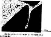
本発明の生成物によれば、破砕路は単一面内ではなく曲がりくねっている。さらに、「微細」とはスプレー後(as-sprayed condition)で200ミクロン未満のケイ素沈殿(precipitate)粒径を有することを意味する。例えば、スプレー後での好ましい沈殿粒径は100ミクロン未満である。エレクトロニックパッケージングの応用に対しては、ケイ素含有量が65%超であることが好ましい。図3および4はスプレー形成され、熱間静圧プレスされたAl80%Siを示し、暗灰色成分はケイ素であり、白色成分はアルミニウムである。実質的に連続したケイ素の相は明確に見えている。
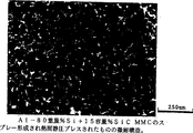
所望により、セラミック粒子を噴霧スプレー中に導入することができる。図5および6は、9μmSiCを略15重量%添加した、スプレー形成され、ヒップされた(hipped)Al−70重量%SiおよびAl−80重量%Siを示し、白色成分はアルミニウムであり、明灰色成分はケイ素であり、暗色成分は炭化ケイ素粒子である。セラミック粒子をスプレー中に注入することができ、粒末を製造するときには、単に粉末材料に添加することができる。
この方法は、該材料を熱間静圧プレスする追加的工程を含むことができる。これは封止(encapsulation)し、またはしないで半固体条件で行われる。
合金材料が、35容量%までの炭化ケイ素のようなセラミック粒子添加剤を含むときは、金属マトリックス複合体材料は半固体条件で封止し、真空にし、熱間静圧プレスすることができる。
本発明の他の態様によれば、
50〜90重量% Si
10〜49重量% Al
0〜10重量% その他の合金添加剤
を含む合金が提供され、ここでケイ素は、合金材料の微細構造内にランダムに配向された微細なケイ素の結晶でできた実質的連続相を形成する。その他の合金添加剤は意図的に添加され、痕跡量の元素を取り除く。添加剤としては次のものが挙げられる。
マグネシウム(2重量%まで)ケイ素相の精錬用
銅(5重量%まで)低熱膨張係数を有する第3相の形成。
鉄(8重量%まで)低熱膨張係数を有する第3相の形成。
ジルコニウム(0.5重量%まで)アルミニウムマトリックスの強化。
添加剤は、アルミニウム合金、特にアルミニウム−ケイ素合金に従来的に添加される任意の合金添加剤を包含する。
所望により、合金材料はSiCのようなセラミック粒体を35容量%まで含有してもよいが、該材料の機械加工性、および金属化を困難にするような大容量ではいけない。本発明による合金またはMMCは、4.5〜11ppm/°Kの範囲の熱膨張係数、および100W/m°Kを超える熱伝導率を有しているのが好適である。達成できる熱伝導率の最大値は補強粒体、例えば窒化アルミニウム、またはダイヤモンドによって決まる。
本発明は、また前記合金を含むマイクロエレクトロニックパッケージング材料も包含する。合金材料は所望の形態のパッケージ部品に半固体加工されおよび/または機械加工される。本発明はまた、他の材料の熱膨張係数と調和させることが必要な応用分野、および/または軽量であることが必要な応用分野、および/または軽量で、かつ異なる膨張係数および/または低熱伝導率の部品を急速に移動させることが必要な応用分野にも適用することができる。
本発明の革新的な特徴は、主成分が合金元素としてのアルミニウムを伴った実質的に連続した相としてのケイ素であるという事実に由来している。ケイ素合金を噴霧することにより、噴霧された小滴が飛翔している間にケイ素の結晶生長が始まり、そしてデポジット中に多数の核形成部位が創り出され、この部位が生長して互いに衝突し、鋳造構造内でケイ素結晶がランダムに配向していて分かれ分かれではなく、高度に配向していない網目構造を形成し、従って、デポジットを実質的にコヒーレントにし、かつ精密表面仕上げ機械加工を可能にする実質的連続相が現れる。
本発明の合金材料の利点は、該材料が通常のカーバイド工具で機械加工可能であり、溶接可能であり、ロウ付け可能であり、金のような材料で被覆可能なことである。
それぞれマイクロ波集積回路(MIC)および多重チップモジュール(MCM)に向けた新規な2つの型の金属マトリックス複合体の予備的データを以下の表1に示す。表2および3は、本発明の合金材料と電子工学産業で使用されている広範囲の半導体およびその他の材料との選択的比較を示している。これらの詳細についてはEuropean Community Project No. BRE2-CT2-0146として1995年11月17日に出版されている。

噴霧ガス 窒素
ガス対金属比 4m3/kg
スプレー距離 700mm
ビレット寸法は好適には径150mmで10kgである。
実施例1
80重量%Si
20重量%Al
この合金のCTEは4.8ppm/℃であり、120W/m°Kの熱伝導率は実施例2のものよりもわずかに低いが、この材料は部品メーカーによって一層容易に機械加工できる。
実施例2
70重量%Si
30重量%Al(SiC15容量%添加)
この合金は6.22ppm/℃のCTEおよび150W/m°Kの熱伝導率を有する。
実施例3
70重量%Si
30重量%Al
CTEは6.8ppm/℃、熱伝導率は140W/m°K。
実施例4
55重量%Si
45重量%Al
CTEは10.5ppm/℃、ヤング率は115GPa、降伏応力は140MPa。The present invention relates to silicon-based alloys, such as silicon-aluminum alloys. The invention also relates to a microelectronic packaging material comprising such an alloy. Furthermore, the present invention relates to a silicon-based alloy requiring a controlled low expansion coefficient.
The electronic package provides a medium for electrical interconnection and support for delicate electronic circuitry. The most basic (zero order level) electronic packaging is a semiconductor chip (integrated circuit) that houses logic gates, transistors and gate-gate connections formed directly on the chip. It is generally considered. The chip itself is made from a thin slice or wafer of crystalline semiconductor material such as silicon or gallium arsenide.
Packaging a chip or a set of chips in a functional protection chip carrier is the next level of electronic packaging. The chip carrier can simply function as a substrate that houses a semiconductor device or to which a semiconductor is attached. Chip carriers range from single chip carriers to more complex multi-chip modules containing many individual chips. Silicon is the most widely used semiconductor for single chip and multichip modules, and gallium arsenide is used for high frequency applications such as microwave integrated circuits.
The term “integration level” refers to the number of microcircuit elements placed on a chip and thus represents its complexity and sophistication. Increasing the electronic circuit elements on the chip while reducing the physical dimensions of the chip, ie increasing the level of integration, is a trend in the electronics industry. As a result of the increased level of integration, the power density increases and thus the heat flux dissipated from the chip surface area is even greater. Therefore, a material having good thermal conductivity is required to satisfy the thermal management requirement when the integration level is increased.
Stress generation at the chip-chip carrier interface, connections and solder joints due to thermal cycling is a major concern in electronic packaging. Therefore, the coefficient of thermal expansion (CTE) of electronic packaging materials is a particularly important material parameter. The close match between the CTE of the chip semiconductor material and the CTE of the chip carrier material reduces the generation of stresses that lead to defects in the electronic circuit elements. Semiconductor materials have a low CTE, for example silicon has a CTE in the range of 2.3 to 4.3 ppm / ° C. and gallium arsenide has a CTE close to 6 ppm / ° C.
Pure aluminum and conventional aluminum alloys are popular as electronic packaging materials for heat dissipation due to their high thermal conductivity in the range of 200-235 w / m ° K. However, as higher integration levels are used in multichip modules and microwave integrated circuits, there is an unmet need for aluminum packages. That is, the thermal expansion mismatch caused by the high CTE in the range of 22-24 ppm / ° C. of these materials.
Other materials, known as KOVAR (registered trade name of Carpenter Technology) and having a CTE of 5.8 ppm / ° C., such as Fe-29Ni-17Co, reduce thermal expansion mismatch with semiconductor materials. However, KOVAR having a thermal conductivity of 15 to 17 w / m ° K is not an optimal material for effective thermal management. Low expansion refractory materials such as molybdenum and tungsten also have low thermal conductivity compared to aluminum. However, composites that produce W-Cu and Mo-Cu mixtures when mixed with copper by powder metallurgy or co-rolling, which are a disadvantage in terms of weight, but which have a higher thermal conductivity are alternative materials. Be guided.
Weight considerations are particularly important in avionics and space applications. One method of manufacturing lightweight electronic packaging materials with high thermal conductivity and low CTE is by an aluminum metal matrix composite (JOM, July 1992, pages 24-28). Silicon carbide granules are a common ceramic reinforcement superior in terms of their low thermal expansion coefficient, high thermal conductivity, good availability and low price compared to other ceramic granules such as aluminum nitride . However, to obtain an aluminum metal matrix composite with the low CTE required for electronic packaging, it is necessary to use 65 to 75 volume percent silicon carbide.
The manufacturing method of the Al / SiC metal matrix composite is classified as follows.
(I) A liquid state process in which ceramic particles are added to a molten matrix alloy and stirred to prevent sedimentation of SiC due to density differences and are cast and molded. However, this method is limited to SiC levels of up to 30% by volume due to flow problems and is limited to certain aluminum alloy matrices that do not produce excess aluminum carbide that reduces mechanical properties and corrosion resistance.
(Ii) A solid state process in which a matrix alloy is mixed with ceramic particles and pressed. From a practical point of view, this method is limited to approximately 60% by volume SiC reinforcement, which limits the resulting CTE reduction.
(Iii) An infiltration process in which the molten matrix alloy is infiltrated into the green SiC compact. Very high SiC particle loadings can be obtained by the infiltration method (up to 75% by volume). Since SiC-Al is non-wetting, it helps penetration by using pressure penetration or by assisting penetration by capillary action by conditioning the SiC particle surface. Although it is possible to obtain a SiC addition amount that requires a CTE that matches the semiconductor material, this metal matrix composite is extremely difficult to machine. Furthermore, since a multi-mode distribution of SiC grain size is required for forming a green compact, this MMC is also difficult to metallize and bond, and is a high vacuum gas required for certain applications. There is a tendency to leak, for example helium leaks in satellite applications.
(Iv) Another method is spray molding in which an aluminum-based alloy is melted, inert gas atomized, and ceramic particles are injected into the co-precipitated metal spray to form a metal matrix composite. Is the method. However, according to this method, the required high addition amount (65 to 75% by volume) of SiC cannot be obtained. This method resulted in excessive porosity, particle agglomeration, and low SiC reproducibility.
Another method for producing an aluminum alloy having a low expansion coefficient is a hypereutectic aluminum-silicon alloy spray forming process in which silicon acts as a reinforcing phase. Instead of introducing the exogenous reinforcing ceramic phase in the form of granules or fibers, the reinforcing phase silicon is generated in situ by nucleating and growing from the liquid while the spray-generated deposit solidifies. The advantage of this method is that the silicon of the intrinsic reinforcing phase is in full atomic contact with the aluminum matrix since the solid state phase making up the alloy is derived from the same source, ie the liquid state alloy. The inventors spray-molded Al-Si alloys with a silicon content of up to 50% by weight. For example, the inventors have published a second international conference on spray molding in 1993 on such alloys, whose main purpose is thixocasting (ie, casting in a semi-solid state to resist Was to produce up to 50% by weight Al-Si alloys for producing wear-structured products. However, it was not possible to make a material containing more than 35% silicon.
In EP-A-411,577, an aluminum-silicon alloy having a Si content of up to 15% by weight is melted, and silicon fine powder having an average particle size of 10 μm or less is preferably injected as a granule to obtain a total silicon content. A method for producing silicon-containing aluminum-based alloys is disclosed which produces spray-formed deposits up to 55% by weight.
According to the first aspect of the present invention, “aluminum-soluble silicon is deliberately sprayed in the form of solid particles and mixed with the aluminum alloy. Thus, a high temperature can be obtained without increasing the melting temperature of the aluminum alloy. An aluminum-based alloy with a silicon content can be produced. ”In one such production example, an aluminum alloy containing 15% by weight of silicon is melted and sprayed to produce silicon particles having an average particle size of 3 μm with a total silicon content. Deposits were made simultaneously in amounts of 35%, 45% and 55% by weight. The casting temperature of the aluminum-15 wt% silicon alloy was 650 ° C.
The present inventors have found that the injection of such a high volume fraction of fine particles results in the following.
(A) a heterogeneous distribution of the injected phase in the matrix;
(B) excess porosity,
(C) High oxide content (to use fine powder with large surface area)
(D) Low yield (because fine particles are carried away by atomizing gas)
Therefore, the present inventors consider that such a method is not practical.
It is known that silicon-aluminum alloys can be produced by melting and casting. For example, the German literature of Chanyuang Gan and Erhard Hornbogen
![]()
According to the present invention, there is provided a method for producing a spray-formed deposit or a gas-sprayed powder using an inert gas spray using a silicon-based alloy.
Therefore, according to the present invention, a method for producing a silicon-based alloy includes melting a silicon alloy containing more than 50% by weight of Si, spraying the alloy with an inert gas, and orienting randomly within the microstructure of the alloy material. Producing a product in which silicon forms a substantially continuous phase made of fine crystals. The product is a coherent spray forming deposit, or powder, and the alloy preferably includes aluminum.
The powder is used for subsequent densification and / or sintering using traditional powder metallurgy methods, or preferably by a hot isostatic press above the solidus temperature.
The coherent spray formed deposit is preferably hot isostatically pressed at a temperature above the solidus to produce a substantially 100% density product.
According to the product of the present invention, the crushing path is winding rather than in a single plane. Further, “fine” means having a silicon precipitate particle size of less than 200 microns after as-sprayed conditions. For example, the preferred precipitated particle size after spraying is less than 100 microns. For electronic packaging applications, it is preferred that the silicon content be greater than 65%. 3 and 4 show Al 80% Si spray formed and hot isostatically pressed, the dark gray component is silicon and the white component is aluminum. The substantially continuous silicon phase is clearly visible.
If desired, ceramic particles can be introduced into the spray spray. FIGS. 5 and 6 show spray-formed, hipped Al-70 wt% Si and Al-80 wt% Si with approximately 15 wt% 9 μm SiC added, the white component is aluminum, light gray The component is silicon and the dark component is silicon carbide particles. Ceramic particles can be injected into the spray and can simply be added to the powder material when producing the powder.
The method can include an additional step of hot isostatic pressing the material. This is done in semi-solid conditions with or without encapsulation.
When the alloy material contains up to 35% by volume ceramic particle additive such as silicon carbide, the metal matrix composite material can be sealed in semi-solid conditions, evacuated and hot isostatically pressed.
According to another aspect of the invention,
50-90 wt% Si
10 to 49% by weight Al
An alloy comprising 0-10% by weight of other alloy additives is provided, wherein the silicon forms a substantially continuous phase made of fine silicon crystals randomly oriented within the microstructure of the alloy material. Other alloy additives are intentionally added to remove trace elements. The following are mentioned as an additive.
Magnesium (up to 2% by weight) Silicon phase refining copper (up to 5% by weight) Formation of a third phase with a low coefficient of thermal expansion.
Iron (up to 8% by weight) formation of a third phase with a low coefficient of thermal expansion.
Zirconium (up to 0.5 wt%) aluminum matrix reinforcement.
Additives include any alloy additive conventionally added to aluminum alloys, particularly aluminum-silicon alloys.
If desired, the alloy material may contain up to 35% by volume of ceramic particles such as SiC, but it should not be so large that the material is difficult to machine and metallize. The alloy or MMC according to the present invention preferably has a coefficient of thermal expansion in the range of 4.5-11 ppm / ° K and a thermal conductivity of more than 100 W / m ° K. The maximum value of thermal conductivity that can be achieved depends on the reinforcing particles, such as aluminum nitride or diamond.
The invention also encompasses microelectronic packaging materials comprising the alloy. The alloy material is semi-solid processed and / or machined into the desired form of the package part. The present invention also provides applications that need to match the thermal expansion coefficients of other materials, and / or applications that need to be lightweight, and / or that are lightweight and have different expansion coefficients and / or low thermal conductivity. It can also be applied in application fields where it is necessary to rapidly move parts of the rate.
The innovative feature of the present invention stems from the fact that the main component is silicon as a substantially continuous phase with aluminum as the alloying element. By spraying the silicon alloy, silicon crystal growth begins while the sprayed droplets are flying, and multiple nucleation sites are created in the deposit that grow and collide with each other, Within the cast structure, the silicon crystals are randomly oriented and not segregated, forming a highly unoriented network, thus making the deposit substantially coherent and enabling precision surface finish machining A substantially continuous phase appears.
An advantage of the alloy material of the present invention is that it can be machined with conventional carbide tools, can be welded, brazed, and coated with a material such as gold.
Preliminary data for the two new types of metal matrix composites for microwave integrated circuits (MIC) and multichip modules (MCM), respectively, are shown in Table 1 below. Tables 2 and 3 show a selective comparison of the alloy materials of the present invention with a wide range of semiconductors and other materials used in the electronics industry. These details are published on November 17, 1995 as European Community Project No. BRE2-CT2-0146.
Spray gas Nitrogen gas to metal ratio 4m 3 / kg
Spray distance 700mm
The billet dimensions are preferably 10 kg with a diameter of 150 mm.
Example 1
80 wt% Si
20 wt% Al
The CTE of this alloy is 4.8 ppm / ° C. and the thermal conductivity of 120 W / m ° K is slightly lower than that of Example 2, but this material can be more easily machined by component manufacturers.
Example 2
70 wt% Si
30% Al (added 15% SiC by volume)
This alloy has a CTE of 6.22 ppm / ° C. and a thermal conductivity of 150 W / m ° K.
Example 3
70 wt% Si
30 wt% Al
CTE is 6.8 ppm / ° C. and thermal conductivity is 140 W / m ° K.
Example 4
55 wt% Si
45 wt% Al
CTE is 10.5 ppm / ° C., Young's modulus is 115 GPa, and yield stress is 140 MPa.
Claims (15)
この合金を、噴霧された小滴が飛翔している間にケイ素の結晶成長が始まるように不活性ガス噴霧し、それにより、
多数のケイ素の核形成部位が創り出され、この部位が成長しお互いに衝突して、ランダムに配向している微細結晶からなるケイ素の実質的な連続相が形成されるように、コヒーレントなデポジットをスプレー形成することを特徴とする、アルミニウム−ケイ素合金デポジットの製造方法であって、
前記デポジットの熱膨張係数が、4.5〜11ppm/°Kであり、
熱伝導率が、100W/m°Kを超えることを特徴とする方法。 Melting the silicon alloy, - aluminum containing 51-90% by weight of silicon
This alloy is sprayed with an inert gas so that silicon crystal growth begins while the sprayed droplets are flying , thereby
A coherent deposit is created so that a number of silicon nucleation sites are created and grow and collide with each other to form a substantially continuous phase of silicon consisting of randomly oriented fine crystals. A method for producing an aluminum-silicon alloy deposit, characterized by spraying comprising:
The deposit has a thermal expansion coefficient of 4.5 to 11 ppm / ° K.
A method wherein the thermal conductivity exceeds 100 W / m ° K.
熱膨張係数が4.5〜11ppm/°Kであり、
熱伝導率が100W/m°Kを超える値であり、かつ
請求の範囲第1項に記載の方法で得られる、合金。Substantially continuous phase made of microcrystals of silicon oriented randomly within the microstructure alloy material silicon is formed, silicon 5 1 90 wt%, aluminum 10 to 49% by weight, and, other alloys additives 0-10% a including alloy,
The coefficient of thermal expansion is 4.5-11 ppm / ° K,
The thermal conductivity is a value exceeding 100 W / m ° K, and
An alloy obtained by the method according to claim 1 .
Applications Claiming Priority (3)
| Application Number | Priority Date | Filing Date | Title |
|---|---|---|---|
| GBGB9514777.3A GB9514777D0 (en) | 1995-07-19 | 1995-07-19 | Silicon alloys for electronic packaging |
| GB9514777.3 | 1995-07-19 | ||
| PCT/GB1996/001730 WO1997003775A1 (en) | 1995-07-19 | 1996-07-18 | Silicon alloys for electronic packaging |
Publications (2)
| Publication Number | Publication Date |
|---|---|
| JPH11509480A JPH11509480A (en) | 1999-08-24 |
| JP3892039B2 true JP3892039B2 (en) | 2007-03-14 |
Family
ID=10777919
Family Applications (1)
| Application Number | Title | Priority Date | Filing Date |
|---|---|---|---|
| JP50643997A Expired - Fee Related JP3892039B2 (en) | 1995-07-19 | 1996-07-18 | Silicon alloy for electronic packaging |
Country Status (9)
| Country | Link |
|---|---|
| US (1) | US6312535B1 (en) |
| EP (1) | EP0839078B1 (en) |
| JP (1) | JP3892039B2 (en) |
| AT (1) | ATE205762T1 (en) |
| DE (1) | DE69615375T2 (en) |
| DK (1) | DK0839078T3 (en) |
| ES (1) | ES2164904T3 (en) |
| GB (2) | GB9514777D0 (en) |
| WO (1) | WO1997003775A1 (en) |
Families Citing this family (12)
| Publication number | Priority date | Publication date | Assignee | Title |
|---|---|---|---|---|
| GB2319668B (en) | 1996-11-23 | 2001-09-12 | Marconi Gec Ltd | Housing for electrical apparatus |
| EP1028476A4 (en) * | 1998-09-08 | 2007-11-28 | Sumitomo Metal Ind | Negative electrode material for nonaqueous electrode secondary battery and method for producing the same |
| JP2002294358A (en) * | 2001-04-02 | 2002-10-09 | Taiheiyo Cement Corp | Thermally conductive composite material |
| US6475263B1 (en) * | 2001-04-11 | 2002-11-05 | Crucible Materials Corp. | Silicon aluminum alloy of prealloyed powder and method of manufacture |
| JP4666337B2 (en) * | 2001-05-24 | 2011-04-06 | フライズ メタルズ インコーポレイテッド | Thermal interface material and heat sink placement |
| JP2007521639A (en) * | 2001-05-24 | 2007-08-02 | フライズ メタルズ インコーポレイテッド | Thermal interface material and solder preform |
| KR100453518B1 (en) * | 2001-11-01 | 2004-10-20 | 한국과학기술연구원 | Method for fabrication of si-al alloy structural material |
| US7259468B2 (en) * | 2004-04-30 | 2007-08-21 | Advanced Chip Engineering Technology Inc. | Structure of package |
| JP4585379B2 (en) * | 2005-06-02 | 2010-11-24 | 太平洋セメント株式会社 | Method for producing metal-ceramic composite material |
| US10217534B2 (en) | 2011-09-23 | 2019-02-26 | Edison Welding Institute, Inc. | Method for joining silicon carbide components to one another |
| US20130075039A1 (en) * | 2011-09-23 | 2013-03-28 | Edison Welding Institute, Inc. | System for fabricating silicon carbide assemblies |
| EP2606996A1 (en) * | 2011-12-23 | 2013-06-26 | EPoS S.r.L. | A method for sintering metal matrix composite materials |
Family Cites Families (8)
| Publication number | Priority date | Publication date | Assignee | Title |
|---|---|---|---|---|
| DE3573137D1 (en) * | 1984-10-03 | 1989-10-26 | Sumitomo Electric Industries | Material for a semiconductor device and process for its manufacture |
| JP3170269B2 (en) * | 1988-06-06 | 2001-05-28 | オスピレイ.メタルス.リミテッド | Spray deposition |
| US5022455A (en) * | 1989-07-31 | 1991-06-11 | Sumitomo Electric Industries, Ltd. | Method of producing aluminum base alloy containing silicon |
| GB9015832D0 (en) * | 1990-07-19 | 1990-09-05 | Osprey Metals Ltd | Introducing means |
| WO1992007676A1 (en) * | 1990-10-31 | 1992-05-14 | Sumitomo Electric Industries, Ltd. | Hypereutectic aluminum/silicon alloy powder and production thereof |
| JPH05331635A (en) * | 1992-05-29 | 1993-12-14 | Kobe Steel Ltd | Al-containing si base alloy target and its manufacture |
| NO175543C (en) * | 1992-11-18 | 1994-10-26 | Elkem As | Silicon-based alloy, process for making such alloy, and process for producing consolidated products from silicon-based alloy |
| JPH0892683A (en) * | 1994-09-27 | 1996-04-09 | Sumitomo Electric Ind Ltd | Nitrified aluminum-silicon powder alloy and its production |
-
1995
- 1995-07-19 GB GBGB9514777.3A patent/GB9514777D0/en active Pending
-
1996
- 1996-07-18 AT AT96924997T patent/ATE205762T1/en not_active IP Right Cessation
- 1996-07-18 ES ES96924997T patent/ES2164904T3/en not_active Expired - Lifetime
- 1996-07-18 GB GB9800723A patent/GB2317900B/en not_active Expired - Fee Related
- 1996-07-18 DK DK96924997T patent/DK0839078T3/en active
- 1996-07-18 EP EP96924997A patent/EP0839078B1/en not_active Expired - Lifetime
- 1996-07-18 JP JP50643997A patent/JP3892039B2/en not_active Expired - Fee Related
- 1996-07-18 DE DE69615375T patent/DE69615375T2/en not_active Expired - Lifetime
- 1996-07-18 WO PCT/GB1996/001730 patent/WO1997003775A1/en active IP Right Grant
-
2000
- 2000-03-27 US US09/535,685 patent/US6312535B1/en not_active Expired - Lifetime
Also Published As
| Publication number | Publication date |
|---|---|
| JPH11509480A (en) | 1999-08-24 |
| US6312535B1 (en) | 2001-11-06 |
| GB2317900A (en) | 1998-04-08 |
| GB9514777D0 (en) | 1995-09-20 |
| EP0839078A1 (en) | 1998-05-06 |
| DE69615375D1 (en) | 2001-10-25 |
| EP0839078B1 (en) | 2001-09-19 |
| GB9800723D0 (en) | 1998-03-11 |
| ES2164904T3 (en) | 2002-03-01 |
| DK0839078T3 (en) | 2001-12-27 |
| GB2317900B (en) | 2000-03-01 |
| DE69615375T2 (en) | 2002-08-14 |
| WO1997003775A1 (en) | 1997-02-06 |
| ATE205762T1 (en) | 2001-10-15 |
Similar Documents
| Publication | Publication Date | Title |
|---|---|---|
| JP3892039B2 (en) | Silicon alloy for electronic packaging | |
| US8575051B2 (en) | Heat sink having a high thermal conductivity | |
| US4830820A (en) | Method for producing material for semiconductor device | |
| JPH08222669A (en) | Heat sink and production thereof | |
| KR20070017185A (en) | Heat sink made froma diamond/copper composite material containing boron | |
| EP1114807A1 (en) | Composite material and semiconductor device using the same | |
| JP5531329B2 (en) | Package based on semiconductor heat dissipation parts | |
| JP2000303126A (en) | Aluminum/diamond composite material and its manufacture | |
| CN109457127B (en) | Preparation method of Si-Al electronic packaging material | |
| KR100519063B1 (en) | Method for fabrication of high silicon Al-Si alloy for electronic packaging material by vacuum arc melting method | |
| JP4360832B2 (en) | Copper alloy | |
| EP1055641A2 (en) | Silicon carbide powder and composite material made thereof and method for manufacturing the powder and material | |
| CN1150343C (en) | SiAl alloy with low expansibility and high thermal conductivity | |
| JPH11269575A (en) | Composite material and heat sink using the same | |
| CN110760722A (en) | Si-Al alloy packaging material and preparation method thereof | |
| US6554053B2 (en) | Method of minimizing the size of primary silicon in Al-Si alloy | |
| JP4275892B2 (en) | Manufacturing method of semiconductor element mounting substrate material | |
| CN100534673C (en) | Method for preparing Si-Al alloy using spray deposition forming process | |
| JP2001284509A (en) | Al-SiC COMPOSITE BODY | |
| JP2001217364A (en) | Al-SiC COMPOSITE | |
| JPS6316458B2 (en) | ||
| JPH1017959A (en) | Composite material and its production | |
| JPH0892681A (en) | Nitrified aluminum-silicon powder alloy and its production | |
| JP2003277875A (en) | Tungsten carbide/copper composite material | |
| WO2003064713A1 (en) | Thermal interface materials; and compositions comprising indium and zinc |
Legal Events
| Date | Code | Title | Description |
|---|---|---|---|
| A131 | Notification of reasons for refusal |
Free format text: JAPANESE INTERMEDIATE CODE: A131 Effective date: 20050315 |
|
| A72 | Notification of change in name of applicant |
Free format text: JAPANESE INTERMEDIATE CODE: A721 Effective date: 20050225 |
|
| A601 | Written request for extension of time |
Free format text: JAPANESE INTERMEDIATE CODE: A601 Effective date: 20050615 |
|
| A602 | Written permission of extension of time |
Free format text: JAPANESE INTERMEDIATE CODE: A602 Effective date: 20050916 |
|
| A521 | Request for written amendment filed |
Free format text: JAPANESE INTERMEDIATE CODE: A523 Effective date: 20050915 |
|
| TRDD | Decision of grant or rejection written | ||
| A01 | Written decision to grant a patent or to grant a registration (utility model) |
Free format text: JAPANESE INTERMEDIATE CODE: A01 Effective date: 20061107 |
|
| A61 | First payment of annual fees (during grant procedure) |
Free format text: JAPANESE INTERMEDIATE CODE: A61 Effective date: 20061206 |
|
| R150 | Certificate of patent or registration of utility model |
Free format text: JAPANESE INTERMEDIATE CODE: R150 |
|
| FPAY | Renewal fee payment (event date is renewal date of database) |
Free format text: PAYMENT UNTIL: 20091215 Year of fee payment: 3 |
|
| FPAY | Renewal fee payment (event date is renewal date of database) |
Free format text: PAYMENT UNTIL: 20101215 Year of fee payment: 4 |
|
| FPAY | Renewal fee payment (event date is renewal date of database) |
Free format text: PAYMENT UNTIL: 20111215 Year of fee payment: 5 |
|
| FPAY | Renewal fee payment (event date is renewal date of database) |
Free format text: PAYMENT UNTIL: 20121215 Year of fee payment: 6 |
|
| FPAY | Renewal fee payment (event date is renewal date of database) |
Free format text: PAYMENT UNTIL: 20121215 Year of fee payment: 6 |
|
| FPAY | Renewal fee payment (event date is renewal date of database) |
Free format text: PAYMENT UNTIL: 20131215 Year of fee payment: 7 |
|
| R250 | Receipt of annual fees |
Free format text: JAPANESE INTERMEDIATE CODE: R250 |
|
| R250 | Receipt of annual fees |
Free format text: JAPANESE INTERMEDIATE CODE: R250 |
|
| LAPS | Cancellation because of no payment of annual fees |