JP3887582B2 - Sputtering equipment - Google Patents
Sputtering equipment Download PDFInfo
- Publication number
- JP3887582B2 JP3887582B2 JP2002182893A JP2002182893A JP3887582B2 JP 3887582 B2 JP3887582 B2 JP 3887582B2 JP 2002182893 A JP2002182893 A JP 2002182893A JP 2002182893 A JP2002182893 A JP 2002182893A JP 3887582 B2 JP3887582 B2 JP 3887582B2
- Authority
- JP
- Japan
- Prior art keywords
- deposition
- plate
- sputtering apparatus
- plasma
- wafer
- Prior art date
- Legal status (The legal status is an assumption and is not a legal conclusion. Google has not performed a legal analysis and makes no representation as to the accuracy of the status listed.)
- Expired - Fee Related
Links
Images


Landscapes
- Physical Vapour Deposition (AREA)
Description
【0001】
【発明の属する技術分野】
本発明は、スパッタリング装置に係り、特にその真空容器の壁面に絶縁物などが付着することを防ぐ防着板を具備したスパッタリング装置に関するものである。なお、スパッタリング装置に限らず、CVD装置,PVD装置,ドライエッチング装置にも適用可能である。
【0002】
【従来の技術】
IC(半導体集積回路)の製造工程では誘電体の成膜が種々行われる。その使用目的は、例えば層間絶縁膜,エッチング,選択的なイオン注入あるいは選択的な電極の形成のためのマスク,パッシベーション,キャパシタの誘電体膜などのためのものが多い。そして、目的ごとに材質あるいはプラズマ処理方法が選択され、例えばCVD,ドライエッチング,スパッタリングなどの種々の処理方法が用いられている。
【0003】
近年、ICの小型化のためにキャパシタの誘電体膜にチタン酸バリウムストロンチウム(BST)、あるいはチタン酸ストロンチウム(STO)などの高誘電体物質のプラズマ処理を行うことが検討されつつある。
【0004】
さらに、センサあるいはアクチュエータ,不揮発性メモリデバイス用にチタン酸ジルコン酸鉛(PZT),ストロンチウムビスマスタンタレート(SBT)といった強誘電体物質のプラズマ処理も検討されている。
【0005】
以下、前述した種々の処理のうち、特に従来のスパッタリング装置を挙げて説明する。
【0006】
図5は従来のスパッタリング装置の概略構成を示す縦断面図であり、このスパッタリング装置は真空引き可能な真空容器51によりスパッタ室を形成しており、スパッタ室の下方にはターゲット52が電極53に固定保持される。電極53は真空容器51とは電気的に絶縁され、また電極53はターゲット52の温度が上昇するのを防ぐために水冷機構(図示せず)を内蔵している。
【0007】
そして、真空容器51の上方にはウエハホルダ54が電極53に対向して平行に配置されており、このウエハホルダ54は真空容器51と電気的に絶縁されて浮遊電位になっている。ウエハホルダ54に基板、例えば半導体ウエハ(以下、ウエハと記す)55が載置される。そして、ウエハホルダ54は、ウエハ55をあらかじめ設定されている所定の温度に維持するための加熱機構(図示せず)を内蔵している。
【0008】
そして、電極53と接地されている真空容器51との間に高周波電源56により、スパッタリング条件にて決められている所定の高周波電力が所定の負のDCバイアスのもとに与えられる。
【0009】
このスパッタリング装置で成膜処理を行うには、ウエハホルダ54上にウエハ55を載置し、図示しない排気口につながる真空ポンプにより真空に引き、次にガス導入口から所定のガス(例えばArガス)を所定流量導入しつつ排気口と真空ポンプとの間に介在する可変コンダクタンスバルブを調節して所定の圧力に調節する。そして、高周波電力を印加してプラズマを発生させターゲットをスパッタする。
【0010】
そこで、ターゲット52から飛散する成分は、ウエハ55上に堆積することにより成膜される。そして、ターゲット52から飛散する成分はウエハ55に向かうものばかりではなく、他の方向に向かうものもある。そのウエハ55以外に向かうものが真空容器51の内壁、あるいは真空容器51内の構造物に付着すると、その清掃が難しくなるため、電極53とウエハホルダ54を取り囲むように防着板57が配置されている。
【0011】
防着板57は金属からなり、真空容器51に電気的に接続されて接地電位となっており、着脱容易な構造にして表面に付着したスパッタ物質が厚くなると、取り外して清掃することができるようにしている。さらに防着板57は、ウエハ55の出し入れのために、図示しないが部分的に退避可能になっている。
【0012】
【発明が解決しようとする課題】
このような従来の防着板を備えたスパッタリング装置において、プラズマ処理中に誘電体材料、特に高・強誘電体材料が発生すると、防着板の表面にも絶縁物が成膜され接地面が見えなくなることがある。このような状態ではプラズマが、防着板の隙間から外に広がり膜が付着していない真空容器の壁面などに向かって放電するようになる。このような状態では安定してプラズマ処理を行うことができなくなる。
【0013】
また、複数のウエハを連続的に処理するような場合、被処理ウエハ以外のウエハまでプラズマにさらされて不良になってしまうという問題がある。
【0014】
また、防着板を二重に設置することが考えられるが、2枚の防着板間で放電が生じるという問題がある。
【0015】
また、付着膜が形成された防着板は、定期的にメンテナンスを行わなければならず、作業効率の面からメンテナンスの周期を延ばすことが望まれている。
【0016】
本発明は、前記従来の問題点を解決するものであって、防着板に絶縁物が付着することによってプラズマが防着板で囲まれた空間から外に広がることを防ぐことのできるスパッタリング装置を提供するものであり、また防着板を二重に配した際、二枚の防着板間で放電が生じることを防ぐことができるスパッタリング装置を提供するものである。さらに、防着板に対するメンテナンスの周期を延ばすことができるスパッタリング装置を提供するものであり、また経時的にプラズマの状態が変化することを防ぐことができるスパッタリング装置を提供するものである。
【0017】
【課題を解決するための手段】
前記目的を達成するため、請求項1に記載の発明は、真空を維持することが可能な真空容器と、前記真空容器内にあり、プラズマによって処理されるウエハが載置されるウエハホルダと、前記ウエハホルダに対向して配設された電極に電力を印加する電源と、前記電極を囲むように配置される防着板とからなるスパッタリング装置において、前記防着板を金属材にて二重にかつ互いに非接触状態に設置し、外側の防着板を接地電位とし、内側の防着板を直流負電位とし、かつ前記内外側の防着板の互いに向かい合う面間の距離が異なるように設定したことを特徴とし、この構成によって、プラズマが防着板の外へ広がることを防ぐことができ、安定してプラズマ処理を行うことができる。また被処理ウエハ以外のウエハがプラズマにさらされることを防ぐことができる。しかも、外側の防着板を接地電位とし、内側の防着板を直流負電位とすることにより、付着した絶縁物を取り除きながらプラズマ処理を行うことができるため、防着板のメンテナンス周期を延ばすことができる。
【0018】
請求項2に記載の発明は、請求項1記載のスパッタリング装置において、二重の防着板において、内側の防着板における内面を絶縁体により被覆したことを特徴とし、この構成によって、徐々に絶縁物が付着して経時的にプラズマの状態を変化することを防ぐことができ、安定してプラズマ処理を行うことができる。
【0019】
請求項3に記載の発明は、請求項1または2記載のスパッタリング装置において、プラズマ処理が誘電体薄膜、あるいは強誘電体薄膜を形成するスパッタリング処理であることを特徴とする。
【0020】
請求項4に記載の発明は、請求項1,2または3記載のスパッタリング装置は、複数のウエハが載置され、前記ウエハを処理位置に順次移動させて連続的に処理させる移動手段を備えたことを特徴とし、この構成によって、複数のウエハに対する自動処理が可能になる。
【0021】
【発明の実施の形態】
以下、本発明の好適な実施形態について図面を参照しながら説明する。なお、以下の説明において、図5にて説明した部材に対応する部材には同一符号を付した。
【0022】
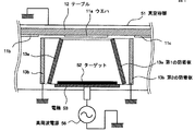
図1は本発明に係るスパッタリング装置の参考例1の概略構成を示す縦断面図であり、参考例1は、真空容器51内に複数のウエハ11a,11b,11cを投入して連続的にプラズマ処理を行い、ウエハ11a,11b,11cに対して絶縁物、特に高・強誘電体材料の成膜を順次行うスパッタリング装置の例である。
【0023】
図1において、真空容器51の下部には、ターゲット52(ターゲットとしては所望の絶縁膜を構成する元素により形成されたもの、または反応性ガスと反応して所望の絶縁物を形成することができる材料が好ましい)を載置した電極53が設置され、また真空容器51の上部には、複数枚のウエハ11a,11b,11cを配置することが可能で、かつ移動可能なウエハホルダであるテーブル12が設けられ、ターゲット52の直上の被処理ウエハ11aに対する成膜が終わると、テーブル12が移動して次のウエハ11bに対する成膜が行われる。
【0024】
ターゲット52を囲むように、二重の金属製筒状体からなる防着板13a,13bが設けられており、内側に設置された第1の防着板13aは浮遊電位であり、外側に設置された第2の防着板13bは接地電位である。両防着板13a,13bは、上部に行くに従って2枚の防着板13a,13b間の距離が離れていき、最上部ではシース厚み(発生するプラズマとの間で電荷の中性が破られ、電場が発生する層領域の距離)以上の間隔となっている。
【0025】
真空容器51中に、不活性ガス(不活性ガスにはHe,Ne,Ar,Kr,Xe,Rnなどがあるが、好ましくはAr)のみ、あるいは不活性ガスと反応性ガス(反応性ガスにはO2,N2などがあるが、成膜したい物質が酸化物ならO2、また窒化物ならN2が好ましい)、あるいは反応性ガスのみを導入し、電極53と真空容器51間に高周波電力(ターゲットが導電性のものであれば直流電力でもよい)を印加する。すると、ターゲット52直上にプラズマが発生し、絶縁物の成膜が開始される。
【0026】
成膜が進行すると、第1の防着板13aと被処理ウエハ11aに絶縁膜が付着して接地面が見えなくなり、プラズマはテーブル12と防着板13a,13b間の隙間から外に広がろうとする。しかし、第2の防着板13bの内面は絶縁物が付着しにくい接地電位面であり、その間に向けて放電が起こるため、二重構造の防着板13a,13bの外にプラズマが広がることはない。
【0027】
以上のことにより、プラズマが二重構造の防着板13a,13bの外側に広がることがなく、安定したプラズマ処理が行え、また、被処理ウエハ11a以外のウエハ11b、11cにプラズマが当たることなくプラズマ処理を行うことができた。
【0028】
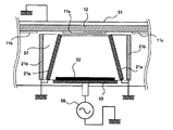
図2は本発明に係るスパッタリング装置の参考例2の概略構成を示す縦断面図であり、参考例2は、参考例1と同様にプラズマ処理を行うスパッタリング装置であって、参考例1の構成と異なる点は、二重構造の防着板21a,21bの両方が接地電位となっている構成である。このような構成にすることにより、両防着板21a,21b間で異常放電が生じることを防ぐことができる。
【0029】
以上のことにより、参考例2では、参考例1と同様に、プラズマが二重構造の防着板21a,21bの外側に広がることがなく、安定したプラズマ処理が行え、また、被処理ウエハ11a以外のウエハ11b,11cにプラズマが当たることなくプラズマ処理を行うことができた。さらに、両防着板間21a,21bで放電が生じることなくプラズマ処理を行うことができた。
【0030】
図3は本発明に係るスパッタリング装置の参考例3の概略構成を示す縦断面図であり、参考例3は、参考例1,2と同様にプラズマ処理を行うスパッタリング装置であって、参考例1,2の構成と異なる点は、二重構造の防着板31a,31bにおける第1の防着板31aの内面32を絶縁物33で被覆した構成である。このように、第1の防着板31aの内面32に既に絶縁物33を形成しておくことにより、成膜を開始してから徐々に絶縁物が付着して行き接地面が見えなくなるまでの間、プラズマの状態が経時的に変化することを防ぐことができる。
【0031】
以上のことにより、参考例3では、参考例1,2における効果に加えて、プラズマの状態が経時的に変化することがなく安定したプラズマ処理を行うことができた。
【0032】
図4は本発明の実施形態を説明するためのスパッタリング装置の概略構成を示す縦断面図であり、本実施形態は、参考例1〜3と同様にプラズマ処理を行うスパッタリング装置であって、参考例1〜3の構成と異なる点は、二重構造の防着板41a,41bにおける第1の防着板41aと第2の防着板41bとを電気的に絶縁し、第2の防着板41bは接地電位に、また第1の防着板41aは直流負電位とした構成である。この構成にしたことにより、第1の防着板41aでもスパッタリング現象が起き、これにより第1の防着板41aの内面32に一旦付着した絶縁物が取り除かれることになる。
【0033】
以上のことにより、本実施形態では、第1の防着板41aの内面32における絶縁物の付着速度が緩和されることにより、メンテナンス周期を延ばすことができた。
【0034】
【発明の効果】
以上説明したように、本発明に係るスパッタリング装置は、防着板を金属材にて二重にかつ互いに非接触状態に設置し、外側の防着板を接地電位とし、内側の防着板を直流負電位とし、かつ前記内外側の防着板の互いに向かい合う面間の距離が異なるように設定したことにより、プラズマが防着板の外へ広がることを防ぐことができ、安定してプラズマ処理を行うことができる。また被処理ウエハ以外のウエハがプラズマにさらされることを防ぐことができる。しかも、外側の防着板を接地電位とし、内側の防着板を直流負電位とすることにより、付着した絶縁物を取り除きながらプラズマ処理を行うことができるため、防着板のメンテナンス周期を延ばすことができる。
【図面の簡単な説明】
【図1】本発明に係るスパッタリング装置の参考例1の概略構成を示す縦断面図
【図2】本発明に係るスパッタリング装置の参考例2の概略構成を示す縦断面図
【図3】本発明に係るスパッタリング装置の参考例3の概略構成を示す縦断面図
【図4】本発明の実施形態を説明するためのスパッタリング装置の概略構成を示す縦断面図
【図5】従来のスパッタリング装置の概略構成を示す縦断面図
【符号の説明】
11a,11b,11c,55 ウエハ
12 テーブル
13a,21a,31a,41a 第1の防着板
13b,21b,31b,41b 第2の防着板
32 第1の防着板の内面
33 絶縁物
51 真空容器
52 ターゲット
53 電極
56 高周波電源[0001]
BACKGROUND OF THE INVENTION
The present invention relates to a sputtering apparatus, and more particularly to a sputtering apparatus provided with a deposition preventing plate that prevents an insulator or the like from adhering to the wall surface of the vacuum vessel. Note that the present invention can be applied not only to a sputtering apparatus but also to a CVD apparatus, a PVD apparatus, and a dry etching apparatus.
[0002]
[Prior art]
In the manufacturing process of an IC (semiconductor integrated circuit), various dielectric films are formed. The purpose of use is often for an interlayer insulating film, etching, mask for selective ion implantation or selective electrode formation, passivation, capacitor dielectric film, and the like. A material or a plasma processing method is selected for each purpose, and various processing methods such as CVD, dry etching, and sputtering are used.
[0003]
In recent years, in order to reduce the size of an IC, it has been studied to perform plasma treatment of a high dielectric material such as barium strontium titanate (BST) or strontium titanate (STO) on a dielectric film of a capacitor.
[0004]
Further, plasma processing of ferroelectric materials such as lead zirconate titanate (PZT) and strontium bismastantalate (SBT) has been studied for sensors, actuators, and nonvolatile memory devices.
[0005]
Hereinafter, among the various processes described above, a conventional sputtering apparatus will be described in particular.
[0006]
FIG. 5 is a longitudinal sectional view showing a schematic configuration of a conventional sputtering apparatus. In this sputtering apparatus, a sputtering chamber is formed by a
[0007]
Above the
[0008]
A predetermined high-frequency power determined by sputtering conditions is applied between the
[0009]
In order to perform the film forming process with this sputtering apparatus, the
[0010]
Therefore, components scattered from the
[0011]
The
[0012]
[Problems to be solved by the invention]
When a dielectric material, particularly a high-ferroelectric material, is generated during plasma processing in such a conventional sputtering apparatus equipped with an adhesion prevention plate, an insulator is formed on the surface of the adhesion prevention plate and a ground plane is formed. It may disappear. In such a state, the plasma spreads out from the gap between the deposition preventing plates and discharges toward the wall surface of the vacuum vessel where no film is attached. In such a state, it becomes impossible to perform plasma processing stably.
[0013]
Further, when processing a plurality of wafers continuously, there is a problem that even wafers other than the wafer to be processed are exposed to plasma and become defective.
[0014]
In addition, although it is conceivable to install the protective plates in a double manner, there is a problem that electric discharge occurs between the two protective plates.
[0015]
In addition, the adhesion-preventing plate on which the adhesion film is formed must be regularly maintained, and it is desired to extend the maintenance cycle from the viewpoint of work efficiency.
[0016]
The present invention solves the above-mentioned conventional problems, and can prevent the plasma from spreading outside from the space surrounded by the deposition preventive plate by attaching an insulator to the deposition preventing plate. In addition, the present invention provides a sputtering apparatus that can prevent discharge between two deposition preventing plates when the deposition preventing plates are doubled. Furthermore, the present invention provides a sputtering apparatus capable of extending the maintenance cycle for the deposition preventing plate, and provides a sputtering apparatus capable of preventing the plasma state from changing over time.
[0017]
[Means for Solving the Problems]
In order to achieve the above object, the invention described in claim 1 includes a vacuum vessel capable of maintaining a vacuum, a wafer holder in the vacuum vessel, on which a wafer to be processed by plasma is placed, and In a sputtering apparatus comprising a power source for applying electric power to an electrode disposed opposite to a wafer holder and an adhesion preventing plate disposed so as to surround the electrode, the adhesion preventing plate is made of a metal material in a double Installed in a non-contact state, set the outer protective plate to ground potential, the inner protective plate to DC negative potential, and the distance between the facing surfaces of the inner and outer protective plates to be different. With this configuration, the plasma can be prevented from spreading out of the deposition preventing plate, and the plasma treatment can be performed stably. Further, it is possible to prevent wafers other than the wafer to be processed from being exposed to plasma. In addition, the plasma treatment can be performed while removing the adhered insulator by setting the outer adhesion plate to the ground potential and the inner adhesion plate to the DC negative potential, thereby extending the maintenance cycle of the adhesion plate. be able to.
[0018]
According to a second aspect of the present invention, in the sputtering apparatus according to the first aspect, in the double anti-adhesion plate, the inner surface of the inner anti-adhesion plate is covered with an insulator, It is possible to prevent an insulating material from adhering and change the plasma state over time, and plasma processing can be performed stably.
[0019]
According to a third aspect of the present invention, in the sputtering apparatus according to the first or second aspect, the plasma treatment is a sputtering treatment for forming a dielectric thin film or a ferroelectric thin film.
[0020]
According to a fourth aspect of the present invention, the sputtering apparatus according to the first, second, or third aspect further includes a moving unit on which a plurality of wafers are placed, and the wafers are sequentially moved to a processing position to be processed continuously. This configuration makes it possible to automatically process a plurality of wafers.
[0021]
DETAILED DESCRIPTION OF THE INVENTION
Preferred embodiments of the present invention will be described below with reference to the drawings. In the following description, members corresponding to those described in FIG.
[0022]
FIG. 1 is a longitudinal sectional view showing a schematic configuration of Reference Example 1 of the sputtering apparatus according to the present invention. In Reference Example 1, a plurality of
[0023]
In FIG. 1, a target 52 (a target formed of an element constituting a desired insulating film as a target, or a reactive gas can be reacted with a reactive gas to form a desired insulator below the
[0024]
The
[0025]
In the
[0026]
As the film formation progresses, an insulating film adheres to the
[0027]
As described above, plasma does not spread outside the double-layer
[0028]
FIG. 2 is a longitudinal sectional view showing a schematic configuration of Reference Example 2 of the sputtering apparatus according to the present invention. Reference Example 2 is a sputtering apparatus that performs plasma processing in the same manner as Reference Example 1, and the configuration of Reference Example 1 is shown in FIG. The difference is that the double-layer
[0029]
As described above, in Reference Example 2, as in Reference Example 1, plasma does not spread outside the double-layer
[0030]
FIG. 3 is a longitudinal sectional view showing a schematic configuration of Reference Example 3 of the sputtering apparatus according to the present invention. Reference Example 3 is a sputtering apparatus that performs plasma processing in the same manner as Reference Examples 1 and 2, and Reference Example 1 , 2 is a configuration in which the
[0031]
As described above, in Reference Example 3, in addition to the effects in Reference Examples 1 and 2, it was possible to perform stable plasma processing without the plasma state changing over time.
[0032]
FIG. 4 is a longitudinal sectional view showing a schematic configuration of a sputtering apparatus for explaining an embodiment of the present invention. This embodiment is a sputtering apparatus for performing plasma processing in the same manner as in Reference Examples 1 to 3, and The difference from the configurations of Examples 1 to 3 is that the
[0033]
As described above, in the present embodiment, the maintenance cycle can be extended by reducing the adhesion speed of the insulator on the
[0034]
【The invention's effect】
As described above, in the sputtering apparatus according to the present invention, the adhesion preventing plates are doubled with a metal material and are not in contact with each other, the outer adhesion preventing plate is set to the ground potential, and the inner adhesion preventing plate is By setting the negative DC potential and the distance between the facing surfaces of the inner and outer protective plates different from each other, it is possible to prevent the plasma from spreading out of the protective plate and to stably perform plasma processing. It can be performed. Further, it is possible to prevent wafers other than the wafer to be processed from being exposed to plasma. In addition, the plasma treatment can be performed while removing the adhered insulator by setting the outer adhesion plate to the ground potential and the inner adhesion plate to the DC negative potential, thereby extending the maintenance cycle of the adhesion plate. be able to.
[Brief description of the drawings]
FIG. 1 is a longitudinal sectional view showing a schematic configuration of Reference Example 1 of a sputtering apparatus according to the present invention. FIG. 2 is a longitudinal sectional view showing a schematic configuration of Reference Example 2 of a sputtering apparatus according to the present invention. FIG. 4 is a longitudinal sectional view showing a schematic configuration of a sputtering apparatus for explaining an embodiment of the present invention. FIG. 5 is a schematic view of a conventional sputtering apparatus. Longitudinal sectional view showing configuration 【Explanation of symbols】
11a, 11b, 11c, 55
Claims (4)
Priority Applications (1)
| Application Number | Priority Date | Filing Date | Title |
|---|---|---|---|
| JP2002182893A JP3887582B2 (en) | 2002-06-24 | 2002-06-24 | Sputtering equipment |
Applications Claiming Priority (1)
| Application Number | Priority Date | Filing Date | Title |
|---|---|---|---|
| JP2002182893A JP3887582B2 (en) | 2002-06-24 | 2002-06-24 | Sputtering equipment |
Publications (3)
| Publication Number | Publication Date |
|---|---|
| JP2004031493A JP2004031493A (en) | 2004-01-29 |
| JP2004031493A5 JP2004031493A5 (en) | 2005-10-27 |
| JP3887582B2 true JP3887582B2 (en) | 2007-02-28 |
Family
ID=31179267
Family Applications (1)
| Application Number | Title | Priority Date | Filing Date |
|---|---|---|---|
| JP2002182893A Expired - Fee Related JP3887582B2 (en) | 2002-06-24 | 2002-06-24 | Sputtering equipment |
Country Status (1)
| Country | Link |
|---|---|
| JP (1) | JP3887582B2 (en) |
Families Citing this family (5)
| Publication number | Priority date | Publication date | Assignee | Title |
|---|---|---|---|---|
| JP4720625B2 (en) * | 2006-06-05 | 2011-07-13 | パナソニック株式会社 | Sputtering equipment |
| JP5186297B2 (en) * | 2008-07-07 | 2013-04-17 | 株式会社アルバック | Sputtering equipment |
| KR101073557B1 (en) * | 2009-11-24 | 2011-10-14 | 삼성모바일디스플레이주식회사 | Sputtering Apparatus |
| JP5982678B2 (en) * | 2012-07-27 | 2016-08-31 | 株式会社ユーテック | Plasma CVD apparatus and method for manufacturing magnetic recording medium |
| WO2018216226A1 (en) * | 2017-05-26 | 2018-11-29 | アドバンストマテリアルテクノロジーズ株式会社 | Film-forming device and film-forming method |
-
2002
- 2002-06-24 JP JP2002182893A patent/JP3887582B2/en not_active Expired - Fee Related
Also Published As
| Publication number | Publication date |
|---|---|
| JP2004031493A (en) | 2004-01-29 |
Similar Documents
| Publication | Publication Date | Title |
|---|---|---|
| US5460689A (en) | High pressure plasma treatment method and apparatus | |
| US20070182327A1 (en) | Manufacturing method of electrode for atmospheric pressure plasma, electrode structure, and atmospheric pressure plasma apparatus using the same | |
| US20070004208A1 (en) | Plasma etching apparatus and plasma etching method | |
| TWI409872B (en) | A plasma processing apparatus, a plasma processing method, and a computer memory medium | |
| KR100782621B1 (en) | Plasma processing method and plasma processing device | |
| JP4642809B2 (en) | Plasma processing method and plasma processing apparatus | |
| JP3887582B2 (en) | Sputtering equipment | |
| US9773665B1 (en) | Particle reduction in a physical vapor deposition chamber | |
| TW201840875A (en) | Paste method to reduce defects in dielectric sputtering | |
| JP4179047B2 (en) | Plasma processing equipment | |
| JP2008098339A (en) | Plasma treatment device and plasma treatment method, and cleaning method of plasma treatment device | |
| JP2001308077A (en) | Semiconductor device manufacturing apparatus | |
| CN115029672B (en) | Sputtering method and method for manufacturing semiconductor device | |
| JP3398027B2 (en) | Vapor phase growth apparatus and cleaning method thereof | |
| US6147011A (en) | Methods of forming dielectric layers and methods of forming capacitors | |
| JP4364335B2 (en) | Sputtering equipment | |
| KR20040096380A (en) | Method for cleaning of chamber for depositing metal oxide and apparatus for depositing to performing the same | |
| JP2006253275A (en) | Sputtering apparatus | |
| JP2009275281A (en) | Sputtering method and system | |
| JP4141022B2 (en) | Sputtering method and sputtering apparatus | |
| JP2007042919A (en) | Sputtering system | |
| CN115058695B (en) | Sputtering method and method for manufacturing semiconductor device | |
| JP4734864B2 (en) | Sputtering method | |
| JP2000345334A (en) | Sputtering device | |
| JP4715736B2 (en) | Sputtering equipment |
Legal Events
| Date | Code | Title | Description |
|---|---|---|---|
| A621 | Written request for application examination |
Free format text: JAPANESE INTERMEDIATE CODE: A621 Effective date: 20050623 |
|
| A521 | Written amendment |
Free format text: JAPANESE INTERMEDIATE CODE: A523 Effective date: 20050704 |
|
| A977 | Report on retrieval |
Free format text: JAPANESE INTERMEDIATE CODE: A971007 Effective date: 20051101 |
|
| A131 | Notification of reasons for refusal |
Free format text: JAPANESE INTERMEDIATE CODE: A131 Effective date: 20060829 |
|
| A521 | Written amendment |
Free format text: JAPANESE INTERMEDIATE CODE: A523 Effective date: 20061026 |
|
| TRDD | Decision of grant or rejection written | ||
| A01 | Written decision to grant a patent or to grant a registration (utility model) |
Free format text: JAPANESE INTERMEDIATE CODE: A01 Effective date: 20061121 |
|
| A61 | First payment of annual fees (during grant procedure) |
Free format text: JAPANESE INTERMEDIATE CODE: A61 Effective date: 20061127 |
|
| R150 | Certificate of patent or registration of utility model |
Free format text: JAPANESE INTERMEDIATE CODE: R150 |
|
| FPAY | Renewal fee payment (event date is renewal date of database) |
Free format text: PAYMENT UNTIL: 20091201 Year of fee payment: 3 |
|
| FPAY | Renewal fee payment (event date is renewal date of database) |
Free format text: PAYMENT UNTIL: 20101201 Year of fee payment: 4 |
|
| FPAY | Renewal fee payment (event date is renewal date of database) |
Free format text: PAYMENT UNTIL: 20111201 Year of fee payment: 5 |
|
| LAPS | Cancellation because of no payment of annual fees |