JP3871981B2 - Semiconductor laser - Google Patents
Semiconductor laser Download PDFInfo
- Publication number
- JP3871981B2 JP3871981B2 JP2002228799A JP2002228799A JP3871981B2 JP 3871981 B2 JP3871981 B2 JP 3871981B2 JP 2002228799 A JP2002228799 A JP 2002228799A JP 2002228799 A JP2002228799 A JP 2002228799A JP 3871981 B2 JP3871981 B2 JP 3871981B2
- Authority
- JP
- Japan
- Prior art keywords
- region
- semiconductor laser
- optical
- current
- injected
- Prior art date
- Legal status (The legal status is an assumption and is not a legal conclusion. Google has not performed a legal analysis and makes no representation as to the accuracy of the status listed.)
- Expired - Fee Related
Links
Images


Landscapes
- Semiconductor Lasers (AREA)
Description
【0001】
【発明の属する技術分野】
本発明は、発振波長を制御しうる半導体レーザに関する。
【0002】
【従来の技術】
現在、大容量光通信ネットワークの基幹伝送系では、光信号を波長軸上で多重化することにより伝送容量の向上を図る波長分割多重(Wavelength Division Multiplexing:WDM)方式が用いられている。
【0003】
しかし、WDM方式では、波長の多重数が増大するに伴い、光源として必要となる半導体レーザの個数も増大する。さらに、バックアップ用光源も光源として用いる半導体レーザと同数以上必要となる。このため、多重数を増大した場合、品種数の増大により在庫管理が煩雑になる。波長可変光源を用いることにより、在庫管理の簡略化を図りたいとの要請があった。
【0004】
また、光通信において波長情報をより積極的に用いようと試みる技術動向もうまれている。例えば、波長の違いによって光信号を光のまま目的とする方向に切り替える波長ルーティングが注目されており、ここでも、発振波長を制御しうる波長可変レーザの開発が望まれていた。
【0005】
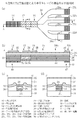
このような波長可変レーザの一つとしては、例えば分布反射型(Distributed Bragg Reflector:DBR)レーザが知られている。従来のDBRレーザについて図38を用いて説明する。図38は従来のDBRレーザの構造を示す断面図である。
【0006】
半導体基板100上に、分布反射鏡領域(DBR領域)102と、利得領域104とが、位相調整領域106を介して設けられている。
【0007】
DBR領域102では、半導体基板100表面に、特定の波長の光を選択的に反射する回折格子からなる分布反射鏡(図示せず)が形成されている。
【0008】
DBR領域102及び位相調整領域106の半導体基板100上には、光閉じ込め層108と、コア層110と、光閉じ込め層112とが順次積層されている。光閉じ込め層112上には、クラッド層114が形成されている。DBR領域102及び位相調整領域106のクラッド層114上には、それぞれ電極116、118が形成されている。
【0009】
利得領域104では、半導体基板100上に、光閉じ込め層120と、活性層122と、光閉じ込め層124とが順次積層されている。光閉じ込め層122上には、クラッド層114が形成されている。クラッド層114上には、活性層122に電流を注入するための電極126が形成されている。
【0010】
上記DBRレーザでは、電極126から利得領域104に電流を注入することによりレーザ発振を得る。このとき、電極116からDBR領域102に電流を注入することにより、発振波長を変化することができる。ただし、この際の発振波長は、共振器損失が最小となる波長に最も近い縦モードに決定されるため、波長は連続的にではなく離散的に変化する。そこで、電極118から位相調整領域106に電流を注入し、その電流量を調整することにより、準連続的な波長変化を実現することが可能となる。このようなDBRレーザの波長可変幅は8nm程度、最大で17nmである。
【0011】
しかし、上述したDBRレーザでは、波長可変幅が狭いため、帯域幅がおよそ30〜40nmのC−バンド或いはL−バンドにわたる波長のレーザ光を得ることはできなかった。C−バンド或いはL−バンドフルカバーの実現は、DBRレーザに対する近年の要請の一つとなっている。
【0012】
かかる要請を背景に、DBRレーザの波長可変幅を拡大し、C−バンド或いはL−バンドフルカバーを実現すべく、以下に述べるような試みがなされている。
【0013】
図39(a)は、2002年3月に開催されたOFC2002において D. C. J. Reid らにより報告された広い波長可変幅を有するDBRレーザの構造を示す断面図である。
【0014】
半導体基板100上に、分布反射鏡領域(DBR領域)102と、利得領域104と、位相調整領域106と、コム(Comb)型反射鏡領域128とが直列に設けられている。
【0015】
DBR領域102は、複数の領域130a、130b、130c、130dに分割されており、各領域130a、130b、130c、130dの半導体基板100表面に、特定の波長の光を選択的に反射する回折格子からなる分布反射鏡(DBR)が形成されている。各領域130a、130b、130c、130dにおけるDBRの回折格子の周期は互いに異なっている。
【0016】
コム型反射鏡領域128の半導体基板100表面には、格子のピッチが徐々に且つ周期的に変化する回折格子からなるコム型反射鏡が設けられている。
【0017】
DBR領域102、位相調整領域106、及びコム型反射鏡領域128の半導体基板100上には、光閉じ込め層108と、コア層110と、光閉じ込め層112とが順次積層されている。光閉じ込め層112上には、クラッド層114が形成されている。DBR領域102の分割された各領域130a、130b、130c、130dのクラッド層114上には、それぞれ電極132a、132b、132c、132dが形成されている。位相調整領域106のクラッド層114上には、電極118が形成されている。コム型反射鏡領域128のクラッド層114上には、電極134が形成されている。
【0018】
利得領域104では、半導体基板100上に、光閉じ込め層120と、活性層122と、光閉じ込め層124とが順次積層されている。光閉じ込め層122上には、クラッド層114が形成されている。クラッド層114上には、活性層122に電流を注入するための電極126が形成されている。
【0019】
レーザ発振の際には、DBR領域102の領域130a、130b、130c、130dのDBRうち、反射スペクトルが所望の発振波長を含むDBRに電流を注入する。電流を注入したDBRとコム型反射鏡領域128とにより、レーザ光の共振器が構成される。
【0020】
複数のDBRのうちから電流を注入するDBRを適宜選択することにより、広い波長可変幅を得ることができる。
【0021】
【発明が解決しようとする課題】
しかしながら、図39(a)に示す従来のDBRレーザでは、複数のDBRが同一導波路内に設けられているので、以下のような難点が存在する。
【0022】
例えば、最も端面に近い領域130aのDBRを選択した場合、その他の領域130b、130c、130cの反射鏡として使用しないDBRを光は通過する。すると、図39(b)に示すように、他のDBRによる反射の影響を受けて一種の複合共振器が構成されることとなる。このため、雑音などの点で悪影響が生じ、通信用光源として用いることは非常に困難であった。
【0023】
また、実際の動作においては、所望の発振波長を帯域に含む1つのDBRだけでなく、複数のDBRに電流を注入することが必要となってくるため、動作制御が複雑なものとなっていた。
【0024】
さらに、選択するDBR領域102のDBRによって共振器長が変動するため、波長可変帯域内で縦モードの間隔が異なり、例えば波長によって副モード抑圧比が変動するなど、レーザ特性が発振波長によって異なってしまっていた。
【0025】
本発明の目的は、通信用光源として求められる特性を失うことなく、広い波長可変幅において所望の波長で発振しうる半導体レーザを提供することにある。
【0026】
【課題を解決するための手段】
上記目的は、電流の注入によりレーザ発振する利得領域と、前記利得領域の一方の側に設けられ、格子のピッチが徐々に且つ周期的に変化する回折格子を有する分布反射鏡を有する第1の領域と、前記利得領域の他方の側に設けられ、互いに異なる周期の回折格子を有する複数の分布反射鏡を有する第2の領域と、前記第1の領域と前記第2の領域との間に設けられ、前記利得領域を介して前記第1の領域の前記分布反射鏡と前記第2の領域の前記複数の分布反射鏡のそれぞれとを光学的に結合する光結合器とを有し、前記第1の領域の前記分布反射鏡と、前記第2の領域の複数の前記分布反射鏡のうちから選択された分布反射鏡とによりレーザ共振器が構成されることを特徴とする半導体レーザにより達成される。
【0027】
【発明の実施の形態】
[第1実施形態]
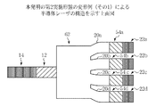
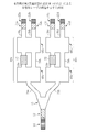
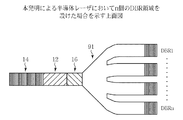
本発明の第1実施形態による半導体レーザ及びその製造方法について図1乃至図3を用いて説明する。図1は本実施形態による半導体レーザの構造を示す概略図、図2は本実施形態による半導体レーザにおける各反射鏡の反射スペクトルを示すグラフ、図3は本実施形態による半導体レーザの製造方法を示す工程断面図である。本実施形態による半導体レーザは、4つのDBR領域を有し、1.5μm帯で発振するDBRレーザを示したものである。
【0028】
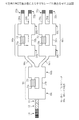
〔1〕半導体レーザ
まず、本実施形態による半導体レーザについて図1を用いて説明する。図1(a)は本実施形態による半導体レーザの構造を示す上面図、図1(b)は図1(a)のA−A′線断面図、図1(c)は図1(a)のB−B′線断面図、図1(d)は図1(a)のC−C′線断面図である。
【0029】
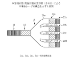
図1(a)及び図1(b)に示すように、本実施形態による半導体レーザでは、n型InP基板10上に、レーザ光となる光を発生する利得領域12が設けられている。利得領域12の一端側のn型InP基板10上には、レーザ光が発振する共振器を構成するコム型反射鏡領域14が設けられている。利得領域12の他端側には、レーザ光の位相を調整する位相調整領域16が設けられている。
【0030】
さらに、n型InP基板10上には、位相調整領域16に入力端が接続され、入力端に導入された光を4つの出力端に分岐し、出力端から導入された光を入力端へ出力する1入力4出力のテーパ状導波路型合流器18が設けられている。
【0031】
テーパ状導波路型合流器18の各出力端には、それぞれn型InP基板10上に形成された光導波路20a、20b、20c、20dが接続されている。各光導波路20a、20b、20c、20dの端部近傍には、レーザ光が発振する共振器をコム型反射鏡領域14とともに構成するDBR領域22a、22b、22c、22dが設けられている。
【0032】
利得領域12では、図1(b)及び図1(c)に示すように、n型InP基板10上に、例えば1.2μm組成のInGaAsPからなる光閉じ込め層24が形成されている。InGaAsPからなる光閉じ込め層24上には、例えば井戸厚5.1nm、バリア厚10nmのInGaAsPからなる6層歪み多重量子井戸(Multi Quantum Well:MQW)層26が形成されている。6層歪みMQW層26上には、例えば1.2μm組成のInGaAsPからなる光閉じ込め層28が形成されている。これら光閉じ込め層24、6層歪みMQW層26、及び光閉じ込め層28は、メサ状に形成されている。このメサ周辺のn型InP基板上には、p型InP埋め込み層30、n型InP電流狭窄層32とが順次積層されており、メサが埋め込まれている。メサ上部の光閉じ込め層28及びn型InP電流狭窄層32上には、p型InPクラッド層34と、p型InGaAsコンタクト層36が順次積層されている。p型InGaAsコンタクト層36上には、電流を注入するための電極38が形成されている。
【0033】
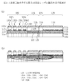
コム型反射鏡領域14では、図1(a)及び図1(b)に示すように、n型InP基板10表面に、格子のピッチが徐々に且つ周期的に変化する回折格子が設けられてなるコム型反射鏡40が形成されている。コム型反射鏡40は、例えば反射率が50%以上の複数の反射ピークを有する分布反射鏡である。
【0034】
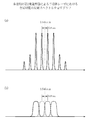
図2(a)はコム型反射鏡40の反射スペクトルの一例を示すグラフである。コム型反射鏡40の回折格子は、その反射スペクトルにおいて、例えば図2(a)に示すように、1.545μmを中心として6.8nmの間隔で反射ピークが並ぶように形成されている。
【0035】
各DBR領域22a、22b、22c、22dでは、図1(a)及び図1(b)に示すように、n型InP基板10表面に、互いに周期の異なる回折格子からなる分布反射鏡42が形成されている。
【0036】
図2(b)は各DBR領域22a、22b、22c、22dに設けられた分布反射鏡42の反射スペクトルの一例を示すグラフである。分布反射鏡42の回折格子は、これらの反射スペクトルにおいて、例えば図2(b)に示すように、1.545μm近辺でそれぞれの分布反射鏡による反射ピークが6.8nm間隔で並ぶように形成されている。
【0037】
利得領域12以外のパッシブ領域、すなわち、コム型反射鏡領域14、位相調整領域16、テーパ状光導波路型光合流器18、各光導波路20a、20b、20c、20d、及びDBR領域22a、22b、22c、22dの断面構造は、ほぼ同様の層構造を有している。これらパッシブ領域の層構造について、光導波路20dの断面を示す図1(d)を例に説明する。
【0038】
パッシブ領域では、n型InP基板10上に、1.2μm組成のInGaAsPからなる光閉じ込め層24が形成されている。InGaAsPからなる光閉じ込め層24上には、InGaAsPからなるコア層44が形成されている。コア層44上には、1.2μm組成のInGaAsPからなる光閉じ込め層28が形成されている。光閉じ込め層24、コア層44、及び光閉じ込め層28は、利得領域と同様にメサ状に形成されている。このメサ周辺のn型InP基板10上には、p型InP埋め込み層30、n型InP電流狭窄層32とが順次積層されており、メサが埋め込まれている。メサ上部の光閉じ込め層28及びn型InP電流狭窄層32上には、p型InPクラッド層34と、p型InGaAsコンタクト層36が順次積層されている。コム型反射鏡領域14、位相調整領域16、及び各DBR領域22a、22b、22c、22dのp型InGaAsコンタクト層36上には、それぞれ各領域に電流を注入するための電極46、48、50が設けられている。
【0039】
このように、本実施形態による半導体レーザは、コム型反射鏡領域14に光結合された一の光路を複数の光路に分岐するテーパ状導波路型光合流器18と、テーパ状導波路型光合流器18により分岐された光路に光結合された各光導波路20a、20b、20c、20dの端部近傍に複数のDBR領域22a、22b、22c、22dが設けられていることに主たる特徴がある。このようにアレイ化されたDBR領域22a、22b、22c、22dのうち、電流を注入するDBR領域を、所望のレーザ光の波長に応じて選択することにより、広い波長可変幅を実現することができる。
【0040】
また、各DBR領域22a、22b、22c、22dは、テーパ状導波路型光合流器18により並列に設けられているので一のDBR領域による発振に対して他のDBR領域が影響することがなく、複合共振器が形成されることもない。これにより、雑音が増加することがなく、例えば通信用光源として要求される特性を失うことなく良好なレーザ特性を得ることができる。
【0041】
次に、本実施形態による半導体レーザの動作について図1及び図2を用いて説明する。
【0042】
まず、利得領域12に電流を注入することにより、6層歪みMQW層26において光を発生する。
【0043】
次いで、アレイ化された複数のDBR領域22a、22b、22c、22dのうちのいずれかに電流を注入することにより、電流を注入したDBR領域により定まるレーザの発振波長帯域を決定する。
【0044】
次いで、コム型反射鏡領域14へ電流を注入する。コム型反射鏡領域14への電流注入量を変えることにより、およその発振波長を決定する。
【0045】
こうして、利得領域12において発生した光は、選択したDBR領域とコム型反射鏡領域14との間を周回する。
【0046】
次いで、位相調整領域16へ電流を注入する。位相調整領域16への電流注入量を調整することにより、最終的に、所望の波長でのレーザ発振を得る。
【0047】
このように、本実施形態による半導体レーザによれば、必要とするレーザ光の波長に応じて、アレイ化された複数のDBR領域22a、22b、22c、22dから電流を注入するDBR領域を適宜選択することにより、広い波長可変幅でレーザ発振を得ることができる。また、複数のDBR領域による複合共振器が形成されることもないので、雑音が増加することがなく、良好なレーザ特性を得ることができる。
【0048】
〔2〕半導体レーザの製造方法
次に、本実施形態による半導体レーザの製造方法ついて図3を用いて説明する。
【0049】
まず、n型InP基板10のコム型反射鏡領域14、及びDBR領域22a、22b、22c、22dとなる領域に、例えば電子ビーム露光法を用いて、所定の回折格子をそれぞれ形成する(図3(a)を参照)。これにより、コム型反射鏡領域14においてコム型反射鏡40が形成され、DBR領域22a、22b、22c、22dにおいて分布反射鏡42が形成される。
【0050】
次いで、例えばMOCVD法により、n型InP基板10上に、1.2μm組成のInGaAsPからなる光閉じ込め層24と、井戸厚5.1nm、バリア厚10nmのInGaAsPからなる6層歪みMQW層26と、1.2μm組成のInGaAsPからなる光閉じ込め層28とを順次積層する(図3(b)を参照)。
【0051】
次いで、リソグラフィ及びエッチング技術を用いて、利得領域12となる領域のみに、光閉じ込め層24、6層歪みMQW層26、及び光閉じ込め層28を残存させる(図3(c)を参照)。
【0052】
次いで、例えばMOCVD法により、露出したn型InP基板10上に、1.2μm組成のInGaAsPからなる光閉じ込め層24と、InGaAsPからなるコア層44と、1.2μm組成のInGaAsPからなる光閉じ込め層28とを順次積層する。
【0053】
次いで、リソグラフィ及びエッチング技術を用いて、コム型反射反射鏡領域14、位相調整領域16、テーパ状導波路型光合流器18、各光導波路20a、20b、20c、20d、各DBR領域22a、22b、22c、22dにおける各層を所定の形状にパターニングする。
【0054】
次いで、例えばMOCVD法により、コム型反射鏡領域14等のパターニングにより露出したn型InP基板10上に、p型InP埋め込み層と、n型InP電流狭窄層とを順次積層し、パターニングされた各層を埋め込む。
【0055】
次いで、例えばMOCVD法により、全面に、p型InPクラッド層34と、p型InGaAsコンタクト層36とを順次積層する。
【0056】
次いで、例えばスパッタ法により、金属膜を形成する。次いで、金属膜をパターニングし、コム型反射鏡領域14、利得領域12、位相調整領域16、及び各DBR領域22a、22b、22c、22dのp型InGaAsコンタクト層36上に、電極46、38、48、50をそれぞれ形成する(図3(d)を参照)。
【0057】
こうして、本実施形態による半導体レーザが形成される。
【0058】
このように、本実施形態によれば、テーパ状導波路型光合流器18により複数のDBR領域が並列に設けられアレイ化されているので、アレイ化された複数のDBR領域22a、22b、22c、22dから電流を注入するDBR領域を適宜選択することにより、広い波長可変幅でレーザ発振を得ることができる。
【0059】
また、各DBR領域22a、22b、22c、22dは、テーパ状導波路型光合流器18により並列に設けられているため、選択した一のDBR領域による発振に他のDBR領域が影響することがなく、複合共振器が形成されることもない。これにより、雑音が増加することがなく、良好なレーザ特性を得ることができる。
【0060】
さらに、選択したDBR領域毎に共振器長が変わらないように設計することが可能であるため、発振波長毎にレーザ特性がばらつくこともない。
【0061】
(変形例(その1))
次に、本実施形態の変形例(その1)による半導体レーザについて図4を用いて説明する。
【0062】
本実施形態では、図1に示すように、位相調整領域16を利得領域12とテーパ状導波路型光合流器18との間に設けたが、位相調整領域16を設ける位置は図1に示す位置に限定されるものではない。本変形例による半導体レーザは、光導波路20a、20b、20c、20dに位相調整領域を設けたものである。
【0063】
すなわち、図4に示すように、利得領域12がテーパ状導波路型光合流器18に直接接続されている。光導波路20a、20b、20c、20dのそれぞれには、位相調整領域54a、54b、54c、54dがDBR領域22a、22b、22c、22dに隣接して設けられている。
【0064】
本変形例による半導体レーザの動作について図4を用いて説明する。
【0065】
まず、利得領域12に電流を注入することにより、6層歪みMQW層26において光を発生する。
【0066】
次いで、アレイ化された複数のDBR領域22a、22b、22c、22dのうちのいずれかに電流を注入することにより、電流を注入したDBR領域により定まるレーザの発振波長帯域を決定する。
【0067】
次いで、コム型反射鏡領域14へ電流を注入する。コム型反射鏡領域14への電流注入量を変えることにより、およその発振波長を決定する。
【0068】
位相調整領域54a、54b、54c、54dのうち、選択したDBR領域と同一の光導波路に設けられた位相調整領域へ電流を注入する。位相調整領域への電流注入量を調整することにより、最終的に、所望の波長でのレーザ発振を得る。
【0069】
(変形例(その2))
次に、本実施形態の変形例(その2)による半導体レーザについて図5を用いて説明する。
【0070】
本実施形態では、図1に示すように、利得領域12をコム型反射鏡領域14と位相調整領域16との間に設けたが、利得領域12を設ける位置は図1に示す位置に限定されるものではない。本変形例による半導体レーザは、光導波路20a、20b、20c、20dに利得領域を設けたものである。
【0071】
すなわち、図5に示すように、コム型反射鏡領域14と位相調整領域16とが直接接続されている。光導波路20a、20b、20c、20dのそれぞれには、利得領域56a、56b、56c、56dがDBR領域22a、22b、22c、22dに隣接して設けられている。
【0072】
本変形例による半導体レーザの動作について図5を用いて説明する。
【0073】
まず、利得領域56a、56b、56c、56dのいずれか、又はDBR領域22a、22b、22c、22dのいずれかに電流を注入する。或いは、同一光導波路に隣接して設けられた一組の利得領域とDBR領域の両者に電流を注入する。これにより、電流を注入したDBR領域又は電流を注入した利得領域に隣接して設けられているDBR領域により決まる発振波長帯域を決定する。
【0074】
次いで、コム型反射鏡領域14へ電流を注入する。コム型反射鏡領域14への電流注入量を変えることにより、およその発振波長を決定する。
【0075】
次いで、位相調整領域16へ電流を注入する。位相調整領域16への電流注入量を調整することにより、縦モードの位置を所望の発振波長に一致させる。
【0076】
次いで、利得領域56a、56b、56c、56dのうち、選択したDBR領域と同一光導波路に設けられた利得領域に電流を注入する。
【0077】
こうして、電流を注入することにより利得領域において発生した光は、選択したDBR領域とコム型反射鏡領域14との間を周回し、最終的に、所望の波長でのレーザ発振を得る。
【0078】
なお、利得領域は、電流を注入していない場合には光の吸収層として機能する。したがって、本変形例のように、各DBR領域22a、22b、22c、22dに隣接して利得領域56a、56b、56c、56dを設けることで、選択していないDBR領域に隣接している利得領域では迷光が吸収され、ノイズを低減することができる。
【0079】
(変形例(その3))
次に、本実施形態の変形例(その3)による半導体レーザについて図6を用いて説明する。本変形例による半導体レーザは、利得領域及び位相調整領域を光導波路20a、20b、20c、20dのそれぞれに設けたものである。
【0080】
すなわち、図6に示すように、コム型反射鏡領域14がテーパ状導波路型光合流器18に直接接続されている。光導波路20a、20b、20c、20dのそれぞれには、利得領域58a、58b、58c、58d、及び位相調整領域60a、60b、60c、60dがDBR領域22a、22b、22c、22dに隣接して設けられている。
【0081】
本変形例による半導体レーザの動作について図6を用いて説明する。
【0082】
まず、利得領域58a、58b、58c、58dのいずれか、又はDBR領域22a、22b、22c、22dのいずれかに電流を注入する。或いは、同一光導波路に隣接して設けられた一組の利得領域とDBR領域の両者に電流を注入する。これにより、電流を注入したDBR領域又は電流を注入した利得領域に隣接して設けられているDBR領域により決まる発振波長帯域を決定する。
【0083】
次いで、コム型反射鏡領域14へ電流を注入する。コム型反射鏡領域14への電流注入量を変えることにより、およその発振波長を決定する。
【0084】
次いで、位相調整領域60a、60b、60c、60dのうち、選択したDBR領域と同一光導波路に設けられた位相調整領域へ電流を注入する。位相調整領域への電流注入量を調整することにより、縦モードの位置を所望の発振波長に一致させる。
【0085】
次いで、利得領域58a、58b、58c、58dのうち、選択したDBR領域と同一光導波路に設けられた利得領域に電流を注入する。
【0086】
こうして、最終的に、所望の波長でのレーザ発振を得る。
【0087】
[第2実施形態]
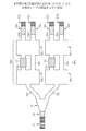
本発明の第2実施形態による半導体レーザについて図7を用いて説明する。図7は本実施形態による半導体レーザの構造を示す上面図である。なお、第1実施形態による半導体レーザと同様の構成要素については同一の符号を付し説明を省略し或いは簡略にする。
【0088】
本実施形態による半導体レーザは、第1実施形態による半導体レーザにおいて、テーパ状導波路型光合流器18の代わりに、多モード干渉型光合流器62を用いたものである。
【0089】
図7に示すように、本実施形態による半導体レーザでは、第1実施形態による場合と同様に、n型InP基板10上に、コム型反射鏡領域14と、利得領域12と、位相調整領域16とが直列に設けられている。
【0090】
さらに、n型InP基板10上には、位相調整領域16に入力端が接続される1入力4出力の多モード干渉型光合流器62が設けられている。多モード干渉型光合流器62の各出力端には、それぞれn型InP基板10上に形成された光導波路20a、20b、20c、20dが接続されている。各光導波路20a、20b、20c、20dの端部近傍には、レーザ光が発振する共振器をコム型反射鏡領域14とともに構成するDBR領域22a、22b、22c、22dが設けられている。
【0091】
このように、本実施形態による半導体レーザでは、テーパ状導波路型光合流器18の代わりに、多モード干渉型光合流器62を用いることに特徴がある。これにより、テーパ状導波路型光合流器18を用いる場合と比較して、より結合損失を低減することができる。
【0092】
本実施形態による半導体レーザは、第1実施形態による半導体レーザの場合とほぼ同様にして動作させることができる。
【0093】
また、本実施形態による半導体レーザは第1実施形態による半導体レーザとほぼ同様にして製造することができる。ここで、多モード干渉型光合流器62については、その他のパッシブ領域と同様にして半導体材料により形成することができる。
【0094】
なお、本実施形態による半導体レーザについても、第1実施形態の変形例による場合と同様に、利得領域、位相調整領域を設ける位置を変更することが可能である。以下に、本実施形態の変形例による半導体レーザについて説明する。
【0095】
(変形例(その1))
本実施形態の変形例(その1)による半導体レーザについて図8を用いて説明する。本変形例による半導体レーザは、第1実施形態の変形例(その1)による場合と同様に、光導波路20a、20b、20c、20dに位相調整領域を設けたものである。
【0096】
すなわち、図8に示すように、利得領域12がテーパ状導波路型光合流器18に直接接続されている。光導波路20a、20b、20c、20dのそれぞれには、位相調整領域54a、54b、54c、54dがDBR領域22a、22b、22c、22dに隣接して設けられている。
【0097】
(変形例(その2))
本実施形態の変形例(その2)による半導体レーザについて図9を用いて説明する。本変形例による半導体レーザは、第1実施形態の変形例(その2)による場合と同様に、光導波路20a、20b、20c、20dに利得領域を設けたものである。
【0098】
すなわち、図9に示すように、コム型反射鏡領域14と位相調整領域16とが直接接続されている。光導波路20a、20b、20c、20dのそれぞれには、利得領域56a、56b、56c、56dがDBR領域22a、22b、22c、22dに隣接して設けられている。
【0099】
(変形例(その3))
本実施形態の変形例(その3)による半導体レーザについて図10を用いて説明する。本変形例による半導体レーザは、第1実施形態の変形例(その3)による場合と同様に、利得領域及び位相調整領域を光導波路20a、20b、20c、20dのそれぞれに設けたものである。
【0100】
すなわち、図6に示すように、コム型反射鏡領域14がテーパ状導波路型光合流器18に直接接続されている。光導波路20a、20b、20c、20dのそれぞれには、利得領域58a、58b、58c、58d、及び位相調整領域60a、60b、60c、60dがDBR領域22a、22b、22c、22dに隣接して設けられている。
【0101】
上述した変形例による半導体レーザは、対応する第1実施形態の変形例による半導体レーザと同様にして動作させることができる。
【0102】
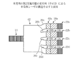
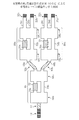
[第3実施形態]
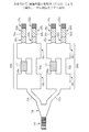
本発明の第3実施形態による半導体レーザについて図11を用いて説明する。なお、第1及び第2実施形態による半導体レーザと同一の構成要素については同一の符号を付し説明を省略し或いは簡略にする。
【0103】
図11に示すように、本実施形態による半導体レーザでは、第1実施形態による場合と同様に、n型InP基板10上に、コム型反射鏡領域14、利得領域12、及び位相調整領域16が直列に設けられている。
【0104】
さらに、n型InP基板10上には、位相調整領域16に入力端が接続する1入力2出力の多モード干渉型スイッチ64が設けられている。多モード干渉型スイッチ64の2つの出力端には、光導波路65a、65bを介して、それぞれn型InP基板10上に形成された1入力2出力のテーパ状導波路型光合流器66a、66bの入力端が接続されている。各テーパ状導波路型光合流器66a、66bの各出力端には、それぞれn型InP基板10上に形成された光導波路20a、20b、20c、20dが接続されている。各光導波路20a、20b、20c、20d端部近傍には、レーザ光が発振する共振器をコム型反射鏡領域14とともに構成するDBR領域22a、22b、22c、22dが設けられている。
【0105】
多モード干渉型スイッチ64は、1入力2出力の多モード干渉計68aと、2入力2出力の多モード干渉計68bと、多モード干渉計68aの出力端と多モード干渉計68bの入力端とをそれぞれ接続する光導波路70a、70bとから構成されている。光導波路70aには、光導波路70aに電流を注入するための電極72が設けられている。多モード干渉計68bの2つの出力端には、それぞれテーパ状導波路型光合流器66a、66bの入力端が接続されている。
【0106】
次に、本実施形態による半導体レーザの動作について図11を用いて説明する。
【0107】
まず、利得領域12に電流を注入することにより、6層歪みMQW層26において光を発生する。
【0108】
次いで、アレイ化された複数のDBR領域22a、22b、22c、22dのうちの一のDBR領域に電流を注入する。これにより、電流を注入したDBR領域により定まるレーザの発振波長帯域を決定する。
【0109】
次いで、コム型反射鏡領域14へ電流を注入する。コム型反射鏡領域14への電流注入量を変えることにより、およその発振波長を決定する。
【0110】
次いで、位相調整領域16へ電流を注入する。位相調整領域16への電流注入量を調整することにより、縦モードの位置を所望の発振波長に一致させる。
【0111】
ここで、利得領域12において発生した光が、電流を注入しているDBR領域とコム型反射鏡領域14との間を周回できるように、多モード干渉型スイッチ64の電極72によって光導波路70aに電流を注入して光路を切り替える。このように、多モード干渉型スイッチ64により共振器が形成される光路を切り替えることにより、テーパ状導波路型光合流器を用いる場合に比べて、光損失を低減することができる。
【0112】
こうして、最終的に、所望の波長でのレーザ発振を得る。
【0113】
このように、本実施形態による半導体レーザによれば、必要とするレーザ光の波長に応じて、アレイ化された複数のDBR領域22a、22b、22c、22dから電流を注入するDBR領域を適宜選択することにより、広い波長可変幅でレーザ発振を得ることができる。これにより、例えば、単一の半導体レーザによるC−バンド或いはL−バンドフルカバーを実現することができる。
【0114】
また、各DBR領域22a、22b、22c、22dは、テーパ状導波路型光合流器18により並列に設けられているため、一のDBR領域による発振に他のDBR領域が影響することがなく、複合共振器が形成されることもない。これにより、雑音が増加することがなく、良好なレーザ特性を得ることができる。
【0115】
さらに、多モード干渉型スイッチ64により、共振器が形成される光路を切り替えるので、光損失を低減することができる。
【0116】
なお、本実施形態による半導体レーザは第1実施形態による半導体レーザとほぼ同様にして製造することができる。ここで、多モード干渉型スイッチ64、テーパ状導波路型光合流器66a、66bについては、その他のパッシブ領域と同様にして半導体材料により形成することができる。
【0117】
また、本実施形態による半導体レーザについても、第1及び第2実施形態の変形例による場合と同様に、利得領域、位相調整領域を設ける位置を変更することが可能である。以下に、本実施形態の変形例による半導体レーザについて説明する。
【0118】
(変形例(その1))
本実施形態の変形例(その1)による半導体レーザについて図12を用いて説明する。本変形例による半導体レーザは、第1実施形態の変形例(その1)による場合と同様に、光導波路20a、20b、20c、20dに位相調整領域を設けたものである。
【0119】
すなわち、図12に示すように、利得領域12が多モード干渉型スイッチ64に直接接続されている。光導波路20a、20b、20c、20dのそれぞれには、位相調整領域54a、54b、54c、54dがDBR領域22a、22b、22c、22dに隣接して設けられている。
【0120】
本変形例による半導体レーザの動作について図12を用いて説明する。
【0121】
まず、利得領域12に電流を注入することにより、6層歪みMQW層26において光を発生する。
【0122】
次いで、アレイ化された複数のDBR領域22a、22b、22c、22dのうちの一のDBR領域に電流を注入する。これにより、電流を注入したDBR領域により定まるレーザの発振波長帯域を決定する。
【0123】
次いで、コム型反射鏡領域14へ電流を注入する。コム型反射鏡領域14への電流注入量を変えることにより、およその発振波長を決定する。
【0124】
次いで、位相調整領域54a、54b、54c、54dのうち、選択したDBR領域と同一の光導波路に設けられた位相調整領域へ電流を注入する。位相調整領域への電流注入量を調整することにより、縦モードの位置を所望の発振波長に一致させる。
【0125】
ここで、利得領域12において発生した光が、電流を注入しているDBR領域とコム型反射鏡領域14との間を周回できるように、多モード干渉型スイッチ64の電極72によって光導波路70aに電流を注入して光路を切り替える。
【0126】
こうして、最終的に、所望の波長でのレーザ発振を得る。
【0127】
(変形例(その2))
本実施形態の変形例(その2)による半導体レーザについて図13を用いて説明する。本変形例による半導体レーザは、第1実施形態の変形例(その2)による場合と同様に、光導波路20a、20b、20c、20dに利得領域を設けたものである。
【0128】
すなわち、図13に示すように、コム型反射鏡領域14と位相調整領域16とが直接接続されている。光導波路20a、20b、20c、20dのそれぞれには、利得領域56a、56b、56c、56dがDBR領域22a、22b、22c、22dに隣接して設けられている。
【0129】
本変形例による半導体レーザの動作について図13を用いて説明する。
【0130】
まず、利得領域56a、56b、56c、56dのいずれか、又はDBR領域22a、22b、22c、22dのいずれかに電流を注入する。或いは、同一光導波路に隣接して設けられた一組の利得領域とDBR領域の両者に電流を注入する。これにより、電流を注入したDBR領域又は電流を注入した利得領域に隣接して設けられているDBR領域により決まる発振波長帯域を決定する。
【0131】
次いで、コム型反射鏡領域14へ電流を注入する。コム型反射鏡領域14への電流注入量を変えることにより、およその発振波長を決定する。
【0132】
次いで、位相調整領域16へ電流を注入する。位相調整領域16への電流注入量を調整することにより、縦モードの位置を所望の発振波長に一致させる。
【0133】
次いで、利得領域56a、56b、56c、56dのうち、選択したDBR領域と同一光導波路に設けられた利得領域に電流を注入する。
【0134】
ここで、利得領域12において発生した光が、電流を注入しているDBR領域とコム型反射鏡領域14との間を周回できるように、多モード干渉型スイッチ64の電極72によって光導波路70aに電流を注入して光路を切り替える。
【0135】
こうして、最終的に、所望の波長でのレーザ発振を得る。
【0136】
(変形例(その3))
本実施形態の変形例(その3)による半導体レーザについて図14を用いて説明する。本変形例による半導体レーザは、第1実施形態の変形例(その3)による場合と同様に、利得領域及び位相調整領域を光導波路20a、20b、20c、20dのそれぞれに設けたものである。
【0137】
すなわち、図14に示すように、コム型反射鏡領域14が多モード干渉型スイッチ64の入力端に直接接続されている。光導波路20a、20b、20c、20dのそれぞれには、利得領域58a、58b、58c、58d、及び位相調整領域60a、60b、60c、60dがDBR領域22a、22b、22c、22dに隣接して設けられている。
【0138】
本変形例による半導体レーザについて図14を用いて説明する。
【0139】
まず、利得領域56a、56b、56c、56dのいずれか、又はDBR領域22a、22b、22c、22dのいずれかに電流を注入する。或いは、同一光導波路に隣接して設けられた一組の利得領域とDBR領域の両者に電流を注入する。これにより、電流を注入したDBR領域又は電流を注入した利得領域に隣接して設けられているDBR領域により決まる発振波長帯域を決定する。
【0140】
次いで、コム型反射鏡領域14へ電流を注入する。コム型反射鏡領域14への電流注入量を変えることにより、およその発振波長を決定する。
【0141】
次いで、位相調整領域60a、60b、60c、60dのうち、選択したDBR領域と同一光導波路に設けられた位相調整領域へ電流を注入する。位相調整領域16への電流注入量を調整することにより、縦モードの位置を所望の発振波長に一致させる。
【0142】
次いで、利得領域58a、58b、58c、58dのうち、選択したDBR領域と同一光導波路に設けられた利得領域に電流を注入する。
【0143】
ここで、利得領域12において発生した光が、電流を注入しているDBR領域とコム型反射鏡領域14との間を周回できるように、多モード干渉型スイッチ64の電極72によって光導波路70aに電流を注入して光路を切り替える。
【0144】
こうして、最終的に、所望の波長でのレーザ発振を得る。
【0145】
(変形例(その4))
本実施形態の変形例(その4)による半導体レーザについて図15を用いて説明する。本変形例による半導体レーザは、多モード干渉型スイッチ64の出力端とテーパ状導波路型光合流器66a、66bとを接続する光導波路65a、65bのそれぞれに、位相調整領域を設けたものである。
すなわち、図15に示すように、利得領域12が多モード干渉型スイッチ64の入力端に直接接続されている。多モード干渉型スイッチ64の一の出力端とテーパ状導波路型光合流器66aの入力端とを接続する光導波路65aには位相調整領域74aが設けられている。多モード干渉型スイッチ64の他の出力端とテーパ状導波路型光合流器66bの入力端とを接続する光導波路65bには位相調整領域74bが設けられている。
【0146】
本変形例による半導体レーザの動作について図15を用いて説明する。
【0147】
まず、DBR領域22a、22b、22c、22dのいずれかに電流を注入する。これにより、電流を注入したDBR領域により決まる発振波長帯域を決定する。
【0148】
次いで、コム型反射鏡領域14へ電流を注入する。コム型反射鏡領域14への電流注入量を変えることにより、およその発振波長を決定する。
【0149】
次いで、位相調整領域74a、74bのうち、選択したDBR領域が接続されたテーパ状導波路型光合流器に接続された光導波路に設けられた位相調整領域へ電流を注入する。位相調整領域16への電流注入量を調整することにより、縦モードの位置を所望の発振波長に一致させる。
【0150】
次いで、利得領域12に電流を注入する。ここで、利得領域12において発生した光が、電流を注入しているDBR領域とコム型反射鏡領域14との間を周回できるように、多モード干渉型スイッチ64の電極72によって光導波路70aに電流を注入して光路を切り替える。
【0151】
こうして、最終的に、所望の波長でのレーザ発振を得る。
【0152】
(変形例(その5))
本実施形態の変形例(その5)による半導体レーザについて図16を用いて説明する。本変形例による半導体レーザは、変形例(その4)による構成において利得領域の位置を変更し、利得領域を光導波路20a、20b、20c、20dのそれぞれに設けたものである。
【0153】
すなわち、図16に示すように、コム型反射鏡領域14が多モード干渉型スイッチ64の入力端に直接接続されている。光導波路20a、20b、20c、20dのそれぞれには、利得領域56a、56b、56c、56dがDBR領域22a、22b、22c、22dに隣接して設けられている。
【0154】
本変形例による半導体レーザの動作について図16を用いて説明する。
【0155】
まず、利得領域56a、56b、56c、56dのいずれか、又はDBR領域22a、22b、22c、22dのいずれかに電流を注入する。或いは、同一光導波路に隣接して設けられた一組の利得領域とDBR領域の両者に電流を注入する。これにより、電流を注入したDBR領域又は電流を注入した利得領域に隣接して設けられているDBR領域により決まる発振波長帯域を決定する。
【0156】
次いで、コム型反射鏡領域14へ電流を注入する。コム型反射鏡領域14への電流注入量を変えることにより、およその発振波長を決定する。
【0157】
次いで、位相調整領域74a、74bのうち、選択したDBR領域が接続されたテーパ状導波路型光合流器に接続された光導波路に設けられた位相調整領域へ電流を注入する。位相調整領域16への電流注入量を調整することにより、縦モードの位置を所望の発振波長に一致させる。
【0158】
次いで、利得領域56a、56b、56c、56dのうち、選択したDBR領域と同一光導波路に設けられた利得領域に電流を注入する。
【0159】
ここで、利得領域12において発生した光が、電流を注入しているDBR領域とコム型反射鏡領域14との間を周回できるように、多モード干渉型スイッチ64の電極72によって光導波路70aに電流を注入して光路を切り替える。
【0160】
こうして、最終的に、所望の波長でのレーザ発振を得る。
【0161】
(変形例(その6))
本実施形態の変形例(その6)による半導体レーザについて図17を用いて説明する。本変形例による半導体レーザは、多モード干渉型スイッチ64の出力端とテーパ状導波路型光合流器66a、66bとを接続する光導波路65a、65bのそれぞれに、利得領域を設けたものである。
すなわち、図17に示すように、利得領域12が多モード干渉型スイッチ64の入力端に直接接続されている。多モード干渉型スイッチ64の一の出力端とテーパ状導波路型光合流器66aの入力端とを接続する光導波路65aには利得領域76aが設けられている。多モード干渉型スイッチ64の他の出力端とテーパ状導波路型光合流器66bの入力端とを接続する光導波路65bには利得領域76bが設けられている。
【0162】
本変形例による半導体レーザの動作について図17を用いて説明する。
【0163】
まず、DBR領域22a、22b、22c、22dのいずれかに電流を注入する。これにより、電流を注入したDBR領域により決まる発振波長帯域を決定する。
【0164】
次いで、コム型反射鏡領域14へ電流を注入する。コム型反射鏡領域14への電流注入量を変えることにより、およその発振波長を決定する。
【0165】
次いで、位相調整領域16へ電流を注入する。位相調整領域16への電流注入量を調整することにより、縦モードの位置を所望の発振波長に一致させる。
【0166】
次いで、利得領域76a、76bのうち、選択したDBR領域が接続されたテーパ状導波路型光合流器に接続された光導波路に設けられた利得領域へ電流を注入する。ここで、利得領域において発生した光が、電流を注入しているDBR領域とコム型反射鏡領域14との間を周回できるように、多モード干渉型スイッチ64の電極72によって光導波路70aに電流を注入して光路を切り替える。
【0167】
こうして、最終的に、所望の波長でのレーザ発振を得る。
【0168】
(変形例(その7))
本実施形態の変形例(その7)による半導体レーザについて図18を用いて説明する。本変形例による半導体レーザは、変形例(その6)による構成において、位相調整領域の位置を変更し、位相調整領域を光導波路20a、20b、20c、20dのそれぞれに設けたものである
すなわち、図18に示すように、コム型反射鏡領域14が多モード干渉型スイッチ64の入力端に直接接続されている。多モード干渉型スイッチ64の一の出力端とテーパ状導波路型光合流器66aの入力端とを接続する光導波路65aには利得領域76aが設けられている。多モード干渉型スイッチ64の他の出力端とテーパ状導波路型光合流器66bの入力端とを接続する光導波路65bには利得領域76bが設けられている。光導波路20a、20b、20c、20dのそれぞれには、位相調整領域54a、54b、54c、54dがDBR領域22a、22b、22c、22dに隣接して設けられている。
【0169】
本変形例による半導体レーザの動作について図18を用いて説明する。
【0170】
まず、DBR領域22a、22b、22c、22dのいずれかに電流を注入する。これにより、電流を注入したDBR領域により決まる発振波長帯域を決定する。
【0171】
次いで、コム型反射鏡領域14へ電流を注入する。コム型反射鏡領域14への電流注入量を変えることにより、およその発振波長を決定する。
【0172】
次いで、位相調整領域54a、54b、54c、54dのうち、選択したDBR領域と同一の光導波路に設けられた位相調整領域へ電流を注入する。位相調整領域への電流注入量を調整することにより、縦モードの位置を所望の発振波長に一致させる。
【0173】
次いで、利得領域76a、76bのうち、選択したDBR領域が接続されたテーパ状導波路型光合流器に接続された光導波路に設けられた利得領域へ電流を注入する。
【0174】
ここで、利得領域において発生した光が、電流を注入しているDBR領域とコム型反射鏡領域14との間を周回できるように、多モード干渉型スイッチ64の電極72によって光導波路70aに電流を注入して光路を切り替える。
【0175】
こうして、最終的に、所望の波長でのレーザ発振を得る。
【0176】
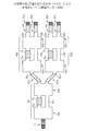
[第4実施形態]
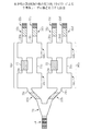
本発明の第4実施形態による半導体レーザについて図19を用いて説明する。図19は本実施形態による半導体レーザの構造を示す上面図である。なお、第1乃至第3実施形態による半導体レーザと同一の構成要素については同一の符号を付し説明を省略し或いは簡略にする。
【0177】
図19に示すように、本実施形態による半導体レーザでは、第1実施形態による場合と同様に、n型InP基板10上に、レーザ光となる光を発生する利得領域12が設けられている。利得領域12の一端側のn型InP基板10上には、レーザ光が発振する共振器を構成するコム型反射鏡領域14が設けられている。利得領域12の他端側には、レーザ光の位相を調整する位相調整領域16が設けられている。
【0178】
さらに、n型InP基板10上には、位相調整領域16に接続する1入力2出力のテーパ状導波路型光合流器78が設けられている。テーパ状導波路型光合流器78の各出力端には、それぞれ光導波路79a、79bを介して、n型InP基板10上に形成された1入力2出力の多モード干渉型スイッチ80a、80bの入力端が接続されている。
【0179】
多モード干渉型スイッチ80a、80bの各出力端には、それぞれn型InP基板10上に形成された光導波路20a、20b、20c、20dが接続されている。各光導波路20a、20b、20c、20d端部近傍には、レーザ光が発振する共振器をコム型反射鏡領域14とともに構成するDBR領域22a、22b、22c、22dが設けられている。
【0180】
多モード干渉型スイッチ80a、80bは、第3実施形態による半導体レーザに用いられている多モード干渉型スイッチ64と同様の構成を有している。
【0181】
次に、本実施形態による半導体レーザの動作について図19を用いて説明する。
【0182】
まず、DBR領域22a、22b、22c、22dのいずれかに電流を注入する。これにより、電流を注入したDBR領域により決まる発振波長帯域を決定する。
【0183】
次いで、コム型反射鏡領域14へ電流を注入する。コム型反射鏡領域14への電流注入量を変えることにより、およその発振波長を決定する。
【0184】
次いで、位相調整領域16へ電流を注入する。位相調整領域16への電流注入量を調整することにより、縦モードの位置を所望の発振波長に一致させる。
【0185】
次いで、利得領域12に電流を注入することにより、6層歪みMQW層26において光を発生する。利得領域12において発生した光は、テーパ状導波路型光合流器78により分岐され、多モード干渉型スイッチ80a、80bに導入される。ここで、利得領域12において発生した光が、電流を注入しているDBR領域とコム型反射鏡領域14との間を周回できるように、多モード干渉型スイッチ80a又は多モード干渉型スイッチ80bの電極72によって光導波路70aに電流を注入して光路を切り替える。
【0186】
こうして、最終的に、所望の波長でのレーザ発振を得る。
【0187】
なお、本実施形態による半導体レーザは第1実施形態による半導体レーザとほぼ同様にして製造することができる。ここで、テーパ状導波路型光合流器78、多モード干渉型スイッチ80a、80bについては、その他のパッシブ領域と同様にして半導体材料により形成することができる。
【0188】
また、本実施形態による半導体レーザについても、第1乃至3実施形態の変形例による場合と同様に、利得領域、位相調整領域を設ける位置を変更することが可能である。以下に、本実施形態の変形例による半導体レーザについて説明する。
【0189】
(変形例(その1))
本実施形態の変形例(その1)による半導体レーザについて図20を用いて説明する。本変形例による半導体レーザは、第1実施形態の変形例(その1)による場合と同様に、光導波路20a、20b、20c、20dに位相調整領域を設けたものである。
【0190】
すなわち、図20に示すように、利得領域12がテーパ状導波路型光合流器78に直接接続されている。光導波路20a、20b、20c、20dのそれぞれには、位相調整領域54a、54b、54c、54dがDBR領域22a、22b、22c、22dに隣接して設けられている。
【0191】
次に、本変形例による半導体レーザの動作について図20を用いて説明する。
【0192】
まず、DBR領域22a、22b、22c、22dのいずれかに電流を注入する。これにより、電流を注入したDBR領域により決まる発振波長帯域を決定する。
【0193】
次いで、コム型反射鏡領域14へ電流を注入する。コム型反射鏡領域14への電流注入量を変えることにより、およその発振波長を決定する。
【0194】
次いで、位相調整領域54a、54b、54c、54dのうち、選択したDBR領域と同一の光導波路に設けられた位相調整領域へ電流を注入する。位相調整領域への電流注入量を調整することにより、縦モードの位置を所望の発振波長に一致させる。
【0195】
次いで、利得領域12に電流を注入することにより、6層歪みMQW層26において光を発生する。ここで、利得領域12において発生した光が、電流を注入しているDBR領域とコム型反射鏡領域14との間を周回できるように、多モード干渉型スイッチ80a又は多モード干渉型スイッチ80bの電極72によって光導波路70aに電流を注入して光路を切り替える。
【0196】
こうして、最終的に、所望の波長でのレーザ発振を得る。
【0197】
(変形例(その2))
本実施形態の変形例(その2)による半導体レーザについて図21を用いて説明する。本変形例による半導体レーザは、第1実施形態の変形例(その2)による場合と同様に、光導波路20a、20b、20c、20dに利得領域を設けたものである。
【0198】
すなわち、図21に示すように、コム型反射鏡領域14と位相調整領域16とが直接接続されている。光導波路20a、20b、20c、20dのそれぞれには、利得領域56a、56b、56c、56dがDBR領域22a、22b、22c、22dに隣接して設けられている。
【0199】
本変形例による半導体レーザの動作について図21を用いて説明する。
まず、利得領域56a、56b、56c、56dのいずれか、又はDBR領域22a、22b、22c、22dのいずれかに電流を注入する。或いは、同一光導波路に隣接して設けられた一組の利得領域とDBR領域の両者に電流を注入する。これにより、電流を注入したDBR領域又は電流を注入した利得領域に隣接して設けられているDBR領域により決まる発振波長帯域を決定する。
【0200】
次いで、コム型反射鏡領域14へ電流を注入する。コム型反射鏡領域14への電流注入量を変えることにより、およその発振波長を決定する。
【0201】
次いで、位相調整領域16へ電流を注入する。位相調整領域への電流注入量を調整することにより、縦モードの位置を所望の発振波長に一致させる。
【0202】
次いで、利得領域12に電流を注入することにより、6層歪みMQW層26において光を発生する。ここで、利得領域12において発生した光が、電流を注入しているDBR領域とコム型反射鏡領域14との間を周回できるように、多モード干渉型スイッチ80a又は多モード干渉型スイッチ80bの電極72によって光導波路70aに電流を注入して光路を切り替える。
【0203】
こうして、最終的に、所望の波長でのレーザ発振を得る。
【0204】
(変形例(その3))
本実施形態の変形例(その3)による半導体レーザについて図22を用いて説明する。本変形例による半導体レーザは、第1実施形態の変形例(その3)による場合と同様に、利得領域及び位相調整領域を光導波路20a、20b、20c、20dのそれぞれに設けたものである。
【0205】
すなわち、図22に示すように、コム型反射鏡領域14がテーパ状導波路型光合流器78に直接接続されている。光導波路20a、20b、20c、20dのそれぞれには、利得領域58a、58b、58c、58d、及び位相調整領域60a、60b、60c、60dがDBR領域22a、22b、22c、22dに隣接して設けられている。
【0206】
本変形例による半導体レーザの動作について図22を用いて説明する。
まず、利得領域58a、58b、58c、58dのいずれか、又はDBR領域22a、22b、22c、22dのいずれかに電流を注入する。或いは、同一光導波路に隣接して設けられた一組の利得領域とDBR領域の両者に電流を注入する。これにより、電流を注入したDBR領域又は電流を注入した利得領域に隣接して設けられているDBR領域により決まる発振波長帯域を決定する。
【0207】
次いで、コム型反射鏡領域14へ電流を注入する。コム型反射鏡領域14への電流注入量を変えることにより、およその発振波長を決定する。
【0208】
次いで、次いで、位相調整領域60a、60b、60c、60dのうち、選択したDBR領域と同一の光導波路に設けられた位相調整領域へ電流を注入する。位相調整領域への電流注入量を調整することにより、縦モードの位置を所望の発振波長に一致させる。
【0209】
次いで、利得領域58a、58b、58c、58dのうち、選択したDBR領域と同一光導波路に設けられた利得領域に電流を注入することにより、6層歪みMQW層26において光を発生する。ここで、利得領域12において発生した光が、電流を注入しているDBR領域とコム型反射鏡領域14との間を周回できるように、多モード干渉型スイッチ80a又は多モード干渉型スイッチ80bの電極72によって光導波路70aに電流を注入して光路を切り替える。
【0210】
こうして、最終的に、所望の波長でのレーザ発振を得る。
【0211】
(変形例(その4))
本実施形態の変形例(その4)による半導体レーザについて図23を用いて説明する。本変形例による半導体レーザは、テーパ状導波路型光合流器78と多モード干渉型スイッチ80a、80bの入力端とを接続する光導波路79a、79bのそれぞれに、位相調整領域を設けたものである。
すなわち、図23に示すように、利得領域12がテーパ状導波路型光合流器78の入力端に直接接続されている。光導波路79a、79bには、それぞれ位相調整領域82a、82bが設けられている。
【0212】
本変形例による半導体レーザの動作について図23を用いて説明する。
【0213】
まず、DBR領域22a、22b、22c、22dのいずれかに電流を注入する。これにより、電流を注入したDBR領域により決まる発振波長帯域を決定する。
【0214】
次いで、コム型反射鏡領域14へ電流を注入する。コム型反射鏡領域14への電流注入量を変えることにより、およその発振波長を決定する。
【0215】
次いで、位相調整領域82a、82bのうち、選択したDBR領域が接続されたモード干渉型光スイッチに接続された光導波路に設けられた位相調整領域へ電流を注入する。位相調整領域への電流注入量を調整することにより、縦モードの位置を所望の発振波長に一致させる。
【0216】
次いで、利得領域12に電流を注入することにより、6層歪みMQW層26において光を発生する。ここで、利得領域12において発生した光が、電流を注入しているDBR領域とコム型反射鏡領域14との間を周回できるように、多モード干渉型スイッチ80a又は多モード干渉型スイッチ80bの電極72によって光導波路70aに電流を注入して光路を切り替える。
【0217】
こうして、最終的に、所望の波長でのレーザ発振を得る。
【0218】
(変形例(その5))
本実施形態の変形例(その5)による半導体レーザについて図24を用いて説明する。本変形例による半導体レーザは、変形例(その4)による構成に加えて、利得領域の位置を変更し、利得領域を光導波路20a、20b、20c、20dのそれぞれに設けたものである。
【0219】
すなわち、光導波路20a、20b、20c、20dのそれぞれには、利得領域56a、56b、56c、56dがDBR領域22a、22b、22c、22dに隣接して設けられている。
【0220】
本変形例による半導体レーザの動作について図24を用いて説明する。
まず、利得領域56a、56b、56c、56dのいずれか、又はDBR領域22a、22b、22c、22dのいずれかに電流を注入する。或いは、同一光導波路に隣接して設けられた一組の利得領域とDBR領域の両者に電流を注入する。これにより、電流を注入したDBR領域又は電流を注入した利得領域に隣接して設けられているDBR領域により決まる発振波長帯域を決定する。
【0221】
次いで、コム型反射鏡領域14へ電流を注入する。コム型反射鏡領域14への電流注入量を変えることにより、およその発振波長を決定する。
【0222】
次いで、位相調整領域82a、82bのうち、選択したDBR領域が接続されたモード干渉型光スイッチに接続された光導波路に設けられた位相調整領域へ電流を注入する。位相調整領域への電流注入量を調整することにより、縦モードの位置を所望の発振波長に一致させる。
【0223】
次いで、利得領域12に電流を注入することにより、6層歪みMQW層26において光を発生する。ここで、利得領域12において発生した光が、電流を注入しているDBR領域とコム型反射鏡領域14との間を周回できるように、多モード干渉型スイッチ80a又は多モード干渉型スイッチ80bの電極72によって光導波路70aに電流を注入して光路を切り替える。
【0224】
こうして、最終的に、所望の波長でのレーザ発振を得る。
【0225】
(変形例(その6))
本実施形態の変形例(その6)による半導体レーザについて図25を用いて説明する。本変形例による半導体レーザは、テーパ状導波路型光合流器78と多モード干渉型スイッチ80a、80bの入力端とを接続する光導波路79a、79bのそれぞれに、利得領域を設けたものである。
すなわち、図25に示すように、コム型反射鏡領域14と位相調整領域16とが直接接続されている。光導波路79a、79bには、それぞれ利得領域84a、84bが設けられている。
【0226】
本変形例による半導体レーザの動作について図25を用いて説明する。
【0227】
まず、DBR領域22a、22b、22c、22dのいずれかに電流を注入する。これにより、電流を注入したDBR領域により決まる発振波長帯域を決定する。
【0228】
次いで、コム型反射鏡領域14へ電流を注入する。コム型反射鏡領域14への電流注入量を変えることにより、およその発振波長を決定する。
【0229】
次いで、位相調整領域16へ電流を注入する。位相調整領域16への電流注入量を調整することにより、縦モードの位置を所望の発振波長に一致させる。
【0230】
次いで、利得領域84a、84bのうち、選択したDBR領域が接続されたモード干渉型光スイッチに接続された光導波路に設けられた利得領域に電流を注入する。これにより、6層歪みMQW層26において光を発生する。ここで、利得領域において発生した光が、電流を注入しているDBR領域とコム型反射鏡領域14との間を周回できるように、多モード干渉型スイッチ80a又は多モード干渉型スイッチ80bの電極72によって光導波路70aに電流を注入して光路を切り替える。
【0231】
こうして、最終的に、所望の波長でのレーザ発振を得る。
【0232】
(変形例(その7))
本実施形態の変形例(その7)による半導体レーザについて図26を用いて説明する。本変形例による半導体レーザは、変形例(その6)による構成における位相調整領域の位置を変え、位相調整領域を光導波路20a、20b、20c、20dのそれぞれに設けたものである。
【0233】
すなわち、図26に示すように、コム型反射鏡領域14がテーパ状導波路型光合流器78に直接接続している。光導波路20a、20b、20c、20dのそれぞれには、位相調整領域54a、54b、54c、54dがDBR領域22a、22b、22c、22dに隣接して設けられている。
【0234】
本変形例による半導体レーザの動作について図26を用いて説明する。
【0235】
まず、DBR領域22a、22b、22c、22dのいずれかに電流を注入する。これにより、電流を注入したDBR領域により決まる発振波長帯域を決定する。
【0236】
次いで、コム型反射鏡領域14へ電流を注入する。コム型反射鏡領域14への電流注入量を変えることにより、およその発振波長を決定する。
【0237】
次いで、位相調整領域54a、54b、54c、54dのうち、選択したDBR領域と同一の光導波路に設けられた位相調整領域へ電流を注入する。位相調整領域への電流注入量を調整することにより、縦モードの位置を所望の発振波長に一致させる。
【0238】
次いで、利得領域84a、84bのうち、選択したDBR領域が接続されたモード干渉型光スイッチに接続された光導波路に設けられた利得領域に電流を注入する。これにより、6層歪みMQW層26において光を発生する。ここで、利得領域において発生した光が、電流を注入しているDBR領域とコム型反射鏡領域14との間を周回できるように、多モード干渉型スイッチ80a又は多モード干渉型スイッチ80bの電極72によって光導波路70aに電流を注入して光路を切り替える。
【0239】
こうして、最終的に、所望の波長でのレーザ発振を得る。
【0240】
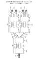
[第5実施形態]
本発明の第5実施形態による半導体レーザについて図27を用いて説明する。図27は本実施形態による半導体レーザの構造を示す上面図である。なお、第1乃至第4実施形態による半導体レーザと同一の構成要素については同一の符号を付し説明を省略し或いは簡略にする。
【0241】
本実施形態による半導体レーザは、第4実施形態による半導体レーザにおけるテーパ状導波路型光合流器78に代わりとして、多モード干渉型スイッチを用いたものである。
【0242】
図27に示すように、本実施形態による半導体レーザでは、第1実施形態による場合と同様に、n型InP基板10上に、レーザ光となる光を発生する利得領域12が設けられている。利得領域12の一端側のn型InP基板10上には、レーザ光が発振する共振器を構成するコム型反射鏡領域14が設けられている。利得領域12の他端側には、レーザ光の位相を調整する位相調整領域16が設けられている。
【0243】
さらに、n型InP基板10上には、位相調整領域16に接続する1入力2出力の多モード干渉型スイッチ86が設けられている。
【0244】
多モード干渉型スイッチ86の各出力端には、それぞれ光導波路88a、88bを介して、n型InP基板10上に形成された多モード干渉型スイッチ80a、80bが設けられている。多モード干渉型スイッチ80a、80bの各出力端には、それぞれn型InP基板10上に形成された光導波路20a、20b、20c、20dが接続されている。各光導波路20a、20b、20c、20d端部近傍には、レーザ光が発振する共振器をコム型反射鏡領域14とともに構成するDBR領域22a、22b、22c、22dが設けられている。
【0245】
多モード干渉型スイッチ86は、第3及び第4実施形態による半導体レーザに用いられている多モード干渉型スイッチ64、80a、80bと同様の構成を有している。
【0246】
次に、本実施形態による半導体レーザについて図27を用いて説明する。
【0247】
まず、DBR領域22a、22b、22c、22dのいずれかに電流を注入する。これにより、電流を注入したDBR領域により決まる発振波長帯域を決定する。
【0248】
次いで、コム型反射鏡領域14へ電流を注入する。コム型反射鏡領域14への電流注入量を変えることにより、およその発振波長を決定する。
【0249】
次いで、位相調整領域16へ電流を注入する。位相調整領域16への電流注入量を調整することにより、縦モードの位置を所望の発振波長に一致させる。
【0250】
次いで、利得領域12に電流を注入することにより、6層歪みMQW層26において光を発生する。利得領域12において発生した光は、多モード干渉型スイッチ86に導入される。ここで、利得領域12において発生した光が、電流を注入しているDBR領域とコム型反射鏡領域14との間を周回できるように、多モード干渉型スイッチ86及び多モード干渉型スイッチ80a又は多モード干渉型スイッチ80bの電極72によって光導波路70aに電流を注入して光路を切り替える。
【0251】
こうして、最終的に、所望の波長でのレーザ発振を得る。
【0252】
本実施形態では、選択したDBR領域とコム型反射鏡領域14との間の光路を多モード干渉型スイッチにより切り替えて構成するので、テーパ状導波路型光合流器による分岐が存在する場合に比べて、光損失を低減することができる。
【0253】
なお、本実施形態による半導体レーザは第1実施形態による半導体レーザとほぼ同様にして製造することができる。ここで、多モード干渉型スイッチ80a、80b、86については、その他のパッシブ領域と同様にして半導体材料により形成することができる。
【0254】
また、本実施形態による半導体レーザについても、第1乃至第4実施形態の変形例による場合と同様に、利得領域、位相調整領域を設ける位置を変更することが可能である。以下に、本実施形態の変形例による半導体レーザについて説明する。
【0255】
(変形例(その1))
本実施形態の変形例(その1)による半導体レーザについて図28を用いて説明する。本変形例による半導体レーザは、第1実施形態の変形例(その1)による場合と同様に、光導波路20a、20b、20c、20dに位相調整領域を設けたものである。
【0256】
すなわち、図28に示すように、利得領域12が多モード干渉型スイッチ86に直接接続されている。光導波路20a、20b、20c、20dのそれぞれには、位相調整領域54a、54b、54c、54dがDBR領域22a、22b、22c、22dに隣接して設けられている。
【0257】
本変形例による半導体レーザの動作について図28を用いて説明する。
【0258】
まず、DBR領域22a、22b、22c、22dのいずれかに電流を注入する。これにより、電流を注入したDBR領域により決まる発振波長帯域を決定する。
【0259】
次いで、コム型反射鏡領域14へ電流を注入する。コム型反射鏡領域14への電流注入量を変えることにより、およその発振波長を決定する。
【0260】
次いで、位相調整領域54a、54b、54c、54dのうち、選択したDBR領域と同一の光導波路に設けられた位相調整領域へ電流を注入する。位相調整領域への電流注入量を調整することにより、縦モードの位置を所望の発振波長に一致させる。
【0261】
次いで、利得領域12に電流を注入することにより、6層歪みMQW層26において光を発生する。ここで、利得領域12において発生した光が、電流を注入しているDBR領域とコム型反射鏡領域14との間を周回できるように、多モード干渉型スイッチ86及び多モード干渉型スイッチ80a又は多モード干渉型スイッチ80bの電極72によって光導波路70aに電流を注入して光路を切り替える。
【0262】
こうして、最終的に、所望の波長でのレーザ発振を得る。
【0263】
(変形例(その2))
本実施形態の変形例(その2)による半導体レーザについて図29を用いて説明する。本変形例による半導体レーザは、第1実施形態の変形例(その2)による場合と同様に、光導波路20a、20b、20c、20dに利得領域を設けたものである。
【0264】
すなわち、図29に示すように、コム型反射鏡領域14と位相調整領域16とが直接接続されている。光導波路20a、20b、20c、20dのそれぞれには、利得領域56a、56b、56c、56dがDBR領域22a、22b、22c、22dに隣接して設けられている。
【0265】
本変形例による半導体レーザの動作について図29を用いて説明する。
まず、利得領域56a、56b、56c、56dのいずれか、又はDBR領域22a、22b、22c、22dのいずれかに電流を注入する。或いは、同一光導波路に隣接して設けられた一組の利得領域とDBR領域の両者に電流を注入する。これにより、電流を注入したDBR領域又は電流を注入した利得領域に隣接して設けられているDBR領域により決まる発振波長帯域を決定する。
【0266】
次いで、コム型反射鏡領域14へ電流を注入する。コム型反射鏡領域14への電流注入量を変えることにより、およその発振波長を決定する。
【0267】
次いで、位相調整領域16へ電流を注入する。位相調整領域への電流注入量を調整することにより、縦モードの位置を所望の発振波長に一致させる。
【0268】
次いで、利得領域12に電流を注入することにより、6層歪みMQW層26において光を発生する。ここで、利得領域12において発生した光が、電流を注入しているDBR領域とコム型反射鏡領域14との間を周回できるように、多モード干渉型スイッチ86及び多モード干渉型スイッチ80a又は多モード干渉型スイッチ80bの電極72によって光導波路70aに電流を注入して光路を切り替える。
【0269】
こうして、最終的に、所望の波長でのレーザ発振を得る。
【0270】
(変形例(その3))
本実施形態の変形例(その3)による半導体レーザについて図30を用いて説明する。本変形例による半導体レーザは、第1実施形態の変形例(その3)による場合と同様に、利得領域及び位相調整領域を光導波路20a、20b、20c、20dのそれぞれに設けたものである。
【0271】
すなわち、図30に示すように、コム型反射鏡領域14が多モード干渉型スイッチ86に直接接続されている。光導波路20a、20b、20c、20dのそれぞれには、利得領域58a、58b、58c、58d、及び位相調整領域60a、60b、60c、60dがDBR領域22a、22b、22c、22dに隣接して設けられている。
【0272】
本変形例による半導体レーザの動作について図30を用いて説明する。
まず、利得領域58a、58b、58c、58dのいずれか、又はDBR領域22a、22b、22c、22dのいずれかに電流を注入する。或いは、同一光導波路に隣接して設けられた一組の利得領域とDBR領域の両者に電流を注入する。これにより、電流を注入したDBR領域又は電流を注入した利得領域に隣接して設けられているDBR領域により決まる発振波長帯域を決定する。
【0273】
次いで、コム型反射鏡領域14へ電流を注入する。コム型反射鏡領域14への電流注入量を変えることにより、およその発振波長を決定する。
【0274】
次いで、次いで、位相調整領域60a、60b、60c、60dのうち、選択したDBR領域と同一の光導波路に設けられた位相調整領域へ電流を注入する。位相調整領域への電流注入量を調整することにより、縦モードの位置を所望の発振波長に一致させる。
【0275】
次いで、利得領域58a、58b、58c、58dのうち、選択したDBR領域と同一光導波路に設けられた利得領域に電流を注入することにより、6層歪みMQW層26において光を発生する。ここで、利得領域12において発生した光が、電流を注入しているDBR領域とコム型反射鏡領域14との間を周回できるように、多モード干渉型スイッチ86及び多モード干渉型スイッチ80a又は多モード干渉型スイッチ80bの電極72によって光導波路70aに電流を注入して光路を切り替える。
【0276】
こうして、最終的に、所望の波長でのレーザ発振を得る。
【0277】
(変形例(その4))
本実施形態の変形例(その4)による半導体レーザについて図31を用いて説明する。本変形例による半導体レーザは、多モード干渉型スイッチ86の出力端と多モード干渉型スイッチ80a、80bの入力端とを接続する光導波路88a、88bのそれぞれに、位相調整領域を設けたものである。
すなわち、図31に示すように、利得領域12が多モード干渉型スイッチ86の入力端に直接接続されている。光導波路88a、88bには、それぞれ位相調整領域82a、82bが設けられている。
【0278】
本変形例による半導体レーザの動作について図31を用いて説明する。
【0279】
まず、DBR領域22a、22b、22c、22dのいずれかに電流を注入する。これにより、電流を注入したDBR領域により決まる発振波長帯域を決定する。
【0280】
次いで、コム型反射鏡領域14へ電流を注入する。コム型反射鏡領域14への電流注入量を変えることにより、およその発振波長を決定する。
【0281】
次いで、位相調整領域82a、82bのうち、選択したDBR領域が接続されたモード干渉型光スイッチに接続された光導波路に設けられた位相調整領域へ電流を注入する。位相調整領域への電流注入量を調整することにより、縦モードの位置を所望の発振波長に一致させる。
【0282】
次いで、利得領域12に電流を注入することにより、6層歪みMQW層26において光を発生する。ここで、利得領域12において発生した光が、電流を注入しているDBR領域とコム型反射鏡領域14との間を周回できるように、多モード干渉型スイッチ86及び多モード干渉型スイッチ80a又は多モード干渉型スイッチ80bの電極72によって光導波路70aに電流を注入して光路を切り替える。
【0283】
こうして、最終的に、所望の波長でのレーザ発振を得る。
【0284】
(変形例(その5))
本実施形態の変形例(その5)による半導体レーザについて図32を用いて説明する。本変形例による半導体レーザは、変形例(その4)による構成に加えて、利得領域を光導波路20a、20b、20c、20dのそれぞれに設けたものである。
【0285】
すなわち、光導波路20a、20b、20c、20dのそれぞれには、利得領域56a、56b、56c、56dがDBR領域22a、22b、22c、22dに隣接して設けられている。
【0286】
本変形例による半導体レーザの動作について図32を用いて説明する。
【0287】
まず、利得領域56a、56b、56c、56dのいずれか、又はDBR領域22a、22b、22c、22dのいずれかに電流を注入する。或いは、同一光導波路に隣接して設けられた一組の利得領域とDBR領域の両者に電流を注入する。これにより、電流を注入したDBR領域又は電流を注入した利得領域に隣接して設けられているDBR領域により決まる発振波長帯域を決定する。
【0288】
次いで、コム型反射鏡領域14へ電流を注入する。コム型反射鏡領域14への電流注入量を変えることにより、およその発振波長を決定する。
【0289】
次いで、位相調整領域82a、82bのうち、選択したDBR領域が接続されたモード干渉型光スイッチに接続された光導波路に設けられた位相調整領域へ電流を注入する。位相調整領域への電流注入量を調整することにより、縦モードの位置を所望の発振波長に一致させる。
【0290】
次いで、利得領域12に電流を注入することにより、6層歪みMQW層26において光を発生する。ここで、利得領域12において発生した光が、電流を注入しているDBR領域とコム型反射鏡領域14との間を周回できるように、多モード干渉型スイッチ86及び多モード干渉型スイッチ80a又は多モード干渉型スイッチ80bの電極72によって光導波路70aに電流を注入して光路を切り替える。
【0291】
こうして、最終的に、所望の波長でのレーザ発振を得る。
【0292】
(変形例(その6))
本実施形態の変形例(その6)による半導体レーザについて図33を用いて説明する。本変形例による半導体レーザは、多モード干渉型スイッチ86の出力端と多モード干渉型スイッチ80a、80bの入力端とを接続する光導波路88a、88bのそれぞれに、利得領域を設けたものである。
すなわち、図33に示すように、コム型反射鏡領域14と位相調整領域16とが直接接続されている。光導波路88a、88bには、それぞれ利得領域84a、84bが設けられている。
【0293】
本変形例による半導体レーザの動作について図33を用いて説明する。
【0294】
まず、DBR領域22a、22b、22c、22dのいずれかに電流を注入する。これにより、電流を注入したDBR領域により決まる発振波長帯域を決定する。
【0295】
次いで、コム型反射鏡領域14へ電流を注入する。コム型反射鏡領域14への電流注入量を変えることにより、およその発振波長を決定する。
【0296】
次いで、位相調整領域16へ電流を注入する。位相調整領域16への電流注入量を調整することにより、縦モードの位置を所望の発振波長に一致させる。
【0297】
次いで、利得領域84a、84bのうち、選択したDBR領域が接続されたモード干渉型光スイッチに接続された光導波路に設けられた利得領域に電流を注入する。これにより、6層歪みMQW層26において光を発生する。ここで、利得領域において発生した光が、電流を注入しているDBR領域とコム型反射鏡領域14との間を周回できるように、多モード干渉型スイッチ86及び多モード干渉型スイッチ80a又は多モード干渉型スイッチ80bの電極72によって光導波路70aに電流を注入して光路を切り替える。
【0298】
こうして、最終的に、所望の波長でのレーザ発振を得る。
【0299】
(変形例(その7))
本実施形態の変形例(その7)による半導体レーザについて図34を用いて説明する。本変形例による半導体レーザは、変形例(その6)による構成における位相調整領域の位置を変え、位相調整領域を光導波路20a、20b、20c、20dのそれぞれに設けたものである。
【0300】
すなわち、図34に示すように、コム型反射鏡領域14が多モード干渉型スイッチ86に直接接続している。光導波路20a、20b、20c、20dのそれぞれには、位相調整領域54a、54b、54c、54dがDBR領域22a、22b、22c、22dに隣接して設けられている。
【0301】
本変形例による半導体レーザの動作について図34を用いて説明する。
【0302】
まず、DBR領域22a、22b、22c、22dのいずれかに電流を注入する。これにより、電流を注入したDBR領域により決まる発振波長帯域を決定する。
【0303】
次いで、コム型反射鏡領域14へ電流を注入する。コム型反射鏡領域14への電流注入量を変えることにより、およその発振波長を決定する。
【0304】
次いで、位相調整領域54a、54b、54c、54dのうち、選択したDBR領域と同一の光導波路に設けられた位相調整領域へ電流を注入する。位相調整領域への電流注入量を調整することにより、縦モードの位置を所望の発振波長に一致させる。
【0305】
次いで、利得領域84a、84bのうち、選択したDBR領域が接続されたモード干渉型光スイッチに接続された光導波路に設けられた利得領域に電流を注入する。これにより、6層歪みMQW層26において光を発生する。ここで、利得領域において発生した光が、電流を注入しているDBR領域とコム型反射鏡領域14との間を周回できるように、多モード干渉型スイッチ86及び多モード干渉型スイッチ80a又は多モード干渉型スイッチ80bの電極72によって光導波路70aに電流を注入して光路を切り替える。
【0306】
こうして、最終的に、所望の波長でのレーザ発振を得る。
【0307】
[変形実施形態]
本発明の上記実施形態に限らず種々の変形が可能である。
【0308】
例えば、上記実施形態では、4つのDBR領域22a、22b、22c、22dを設けていたが、DBR領域の数はこれに限定されるものではない。必要とされる可変波長幅に応じて、回折格子周期の異なる複数のDBR領域をもうけてもよい。例えば、図35は、第1実施形態による半導体レーザにおいて、1入力n出力のテーパ状導波路型光合流器91を用いて、n(nは整数)のDBR領域DBR1、……、DBRnを設けた場合を示す上面図である。
【0309】
また、上記実施形態では、n型InP基板10表面に回折格子を設けたDBR領域を用いたが、回折格子周期が異なるブラッグ回折格子を有するファイバブラッググレーティング(Fiber Bragg Grating:FBG)を用いてもよい。この場合、n型InP基板10上に形成された光導波路に、光ファイバのコア部分に回折格子が作り込まれてなるFBGを光学的に接続する。
【0310】
例えば、図36は、第1実施形態の変形例(その2)による半導体レーザにおいて、DBR領域22a、22b、22c、22dの代わりに、FBG92a、92b、92c、92dを用いた場合を示す上面図である。
【0311】
この場合の半導体レーザの動作について図36を用いて説明する。
【0312】
まず、利得領域56a、56b、56c、56dのいずれかに電流を注入する。これにより、電流を注入した利得領域に隣接して設けられているFBGにより決まる発振波長帯域を決定する。
【0313】
次いで、コム型反射鏡領域14へ電流を注入する。コム型反射鏡領域14への電流注入量を変えることにより、およその発振波長を決定する。
【0314】
次いで、位相調整領域16へ電流を注入する。位相調整領域16への電流注入量を調整することにより、縦モードの位置を所望の発振波長に一致させる。
【0315】
こうして、最終的に、所望の波長でのレーザ発振を得る。
【0316】
また、図37は、第5実施形態による半導体レーザにおいて、DBR領域22a、22b、22c、22dの代わりに、FBG92a、92b、92c、92dを用いた場合を示す上面図である。
【0317】
この場合の半導体レーザの動作について図37を用いて説明する。
【0318】
まず、多モード干渉型スイッチ86及び多モード干渉型スイッチ80a又は多モード干渉型スイッチ80bの電極72によって光導波路70aに電流を注入して光路を切り替え、所定のFBGとコム型反射鏡領域14との間を利得領域12で発生する光が周回できるようにしておく。これにより、そのFBGにより決まる発振波長帯域を決定する。
【0319】
次いで、コム型反射鏡領域14へ電流を注入する。コム型反射鏡領域14への電流注入量を変えることにより、およその発振波長を決定する。
【0320】
次いで、位相調整領域16へ電流を注入する。位相調整領域16への電流注入量を調整することにより、縦モードの位置を所望の発振波長に一致させる。
【0321】
次いで、利得領域12に電流を注入することにより、6層歪みMQW層26において光を発生する。利得領域12において発生した光は、選択したFBGとコム型反射鏡領域14との間を周回し、最終的に、所望の波長でのレーザ発振を得る。
【0322】
上述のように、FBG92a、92b、92c、92dを用いることにより、DBR領域を用いる場合に要した電流注入が不要となり、半導体レーザの動作制御をより簡略化することができる。
【0323】
なお、DBR領域に代えてFBGを用いる場合には、第1及び第2実施形態の変形例(その2)、変形例(その3)、第3、第4及び第5実施形態の変形例(その2)、変形例(その3)、及び変形例(その5)による半導体レーザの場合のように、DBR領域22a、22b、22c、22dのそれぞれに隣接して利得領域56a、56b、56c、56d又は利得領域58a、58b、58c、58dが設けられているか、或いは、第5実施形態による半導体レーザのように、コム型反射鏡14とDBR領域22a、22b、22c、22dとの間の光路を多モード干渉型スイッチにより切り替えることができる必要がある。
【0324】
また、FBGのみならず、例えばPLC(Planar Lightwave Circuit)技術を用いたDBRアレイなどの他の手段をDBR領域として用いることができる。
【0325】
また、上記実施形態において、利得領域の利得の中心波長は、分布反射鏡の反射帯域のほぼ中心値とすることが望ましい。利得領域の利得の中心波長は、必要とされる利得の中心波長に応じて、利得領域を構成する6層歪みMQW層等の活性層のGaInAsPの組成を適宜設定することにより、変更することができる。
【0326】
例えば、第3実施形態の変形例(その6)及び変形例(その7)による半導体レーザにおいては、利得領域76aの利得の中心波長を、利得領域76aが接続するテーパ状導波路型光合流器60aに接続されるDBR領域22a、22bにおける分布反射鏡の反射帯域のほぼ中心値に設定する。同様に、利得領域76bの利得の中心波長を、利得領域76bが接続するテーパ状導波路型光合流器60aに接続されるDBR領域22c、22dにおける分布反射鏡の反射帯域のほぼ中心値に設定する。第4及び第5実施形態の変形例(その6)及び変形例(その7)による半導体レーザにおいても、上記と同様に、利得領域84a、84bの利得の中心波長を、それぞれDBR領域22a、22bにおける分布反射鏡の反射帯域、DBR領域22c、22dにおける分布反射鏡の反射帯域に応じて設定することができる。このとき、利得の中心波長が1538.2nmの場合は、Ga0.296In0.701As0.89P0.11、利得の中心波長が1551.8nmの場合は、Ga0.307In0.693As0.907P0.093とすることができる。
【0327】
また、第1及び第2実施形態の変形例(その2)、変形例(その3)、第3、第4及び第5実施形態の変形例(その2)、変形例(その3)、及び変形例(その5)による半導体レーザの場合のように、DBR領域22a、22b、22c、22dのそれぞれに隣接して利得領域56a、56b、56c、56d又は利得領域58a、58b、58c、58dが設けられている場合には、各利得領域の利得の中心波長を、それぞれ同一光導波路に隣接して設けられているDBR領域における分布反射鏡の反射帯域幅のほぼ中心値に設定する。このとき、利得の中心波長が1534.8nmの場合は、Ga0.296In0.704As0.885P0.115、利得の中心波長が1541.6nmの場合は、Ga0.301In0.699As0.894P0.106、利得の中心波長が1548.4nmの場合は、Ga0.304In0.696As0.91P0.09とすることができる。
【0328】
また、上記実施形態で示した材料系に限らず、GaAs系、GaN系、GaSb系等の他の材料系のDBRレーザについても本発明を適用することができる。
【0329】
また、上記実施形態では、半導体材料を用いて、光導波路、テーパ状導波路型光合流器、多モード干渉型スイッチ等を作製したが、これらの材料は半導体材料に限定されるものではない。例えば、石英系材料を用いて作製してもよい。
【0330】
また、上記実施形態では、テーパ状導波路型光合流器を分岐導波路として用いたが、一の光路を複数の光路に分岐できるものであれば、テーパ状導波路型に限定されるものではない。
【0331】
また、上記実施形態では、多モード干渉型スイッチを光スイッチとして用いたが、一の光路を複数の光路のうちのいずれかの光路に切り替えることができる光スイッチであれば、多モード干渉型に限定されるものではない。
【0332】
また、上記実施形態では、多モード干渉型スイッチは、1つの光路を2つの光路に分岐し、分岐した光路のいずれかを選択するものであったが、2分岐に限られず、複数に分岐した光路のいずれかの光路を選択する光スイッチであってもよい。
【0333】
(付記1) 電流の注入によりレーザ発振する利得領域と、前記利得領域の一方の側に設けられ、格子のピッチが徐々に且つ周期的に変化する回折格子を有する分布反射鏡を有する第1の領域と、前記利得領域の他方の側に設けられ、互いに異なる周期の回折格子を有する複数の分布反射鏡を有する第2の領域と、前記第1の領域と前記第2の領域との間に設けられ、前記利得領域を介して前記第1の領域の前記分布反射鏡と前記第2の領域の前記複数の分布反射鏡のそれぞれとを光学的に結合する光結合器とを有することを特徴とする半導体レーザ。
【0334】
(付記2) 付記1記載の半導体レーザにおいて、前記第1の領域の前記分布反射鏡と前記第2の領域の前記複数の分布反射鏡のそれぞれとにより、複数の共振器が構成されていることを特徴とする半導体レーザ。
【0335】
(付記3) 付記1又は2記載の半導体レーザにおいて、前記光結合器は、前記第1の領域の前記分布反射鏡に光結合された一の光路を、前記第2の領域の前記複数の分布反射鏡のそれぞれに光結合された複数の光路に分岐する分岐導波路を有することを特徴とする半導体レーザ。
【0336】
(付記4) 付記3記載の半導体レーザにおいて、前記分岐導波路は、前記利得領域と前記第2の領域との間に設けられていることを特徴とする半導体レーザ。
【0337】
(付記5) 付記3記載の半導体レーザにおいて、前記分岐導波路は、前記第1の領域と前記利得領域との間に設けられており、前記利得領域は、前記複数の光路のそれぞれに設けられていることを特徴とする半導体レーザ。
【0338】
(付記6) 付記5記載の半導体レーザにおいて、前記第2の領域の前記分布反射鏡は、ファイバーブラッググレーティングであることを特徴とする半導体レーザ。
【0339】
(付記7) 付記4乃至6のいずれかに記載の半導体レーザにおいて、前記分岐導波路は、前記第1の領域の前記分布反射鏡に光結合された一の光路を、前記第2の領域の前記複数の分布反射鏡のそれぞれに光結合された複数の光路に分岐するテーパ状導波路型光合流器又は多モード干渉型光合流器であることを特徴とする半導体レーザ。
【0340】
(付記8)付記4乃至6のいずれかに記載の半導体レーザにおいて、前記分岐導波路は、前記第1の領域の前記分布反射鏡に光結合された一の光路を複数の光路に分岐していずれかの光路を選択する光スイッチと、前記光スイッチにより選択された光路を分岐して前記第2の領域の前記複数の分布反射鏡に光結合する光合流器とを有することを特徴とする半導体レーザ。
【0341】
(付記9)付記4乃至6のいずれかに記載の半導体レーザにおいて、前記分岐導波路は、前記第1の領域の前記分布反射鏡に光結合された一の光路を複数の光路に分岐する光合流器と、前記光合流器により分岐された光路が光結合する前記第2の領域の前記分布反射鏡を選択する光スイッチとを有することを特徴とする半導体レーザ。
【0342】
(付記10)付記4乃至6のいずれかに記載の半導体レーザにおいて、前記分岐導波路は、前記第1の領域の前記分布反射鏡に光結合された一の光路を複数の光路に分岐していずれかの光路を選択する第1の光スイッチと、前記第1の光スイッチにより選択された光路が光結合する前記第2の領域の前記分布反射鏡を選択する第2の光スイッチとを有することを特徴とする半導体レーザ。
【0343】
(付記11)付記1乃至10のいずれかに記載の半導体レーザにおいて、前記第1の領域の前記分布反射鏡と前記第2の領域の前記複数の分布反射鏡のいずれかとの間で発振するレーザ光の位相を調整する位相調整領域を更に有することを特徴とする半導体レーザ。
【0344】
(付記12)付記11記載の半導体レーザにおいて、前記位相調整領域は、前記第1の領域と前記光結合器との間に設けられていることを特徴とする半導体レーザ。
【0345】
(付記13)付記11記載の半導体レーザにおいて、前記位相調整領域は、前記光結合器と前記第2の領域の前記複数の分布反射鏡との間に設けられていることを特徴とする半導体レーザ。
【0346】
(付記14)付記3記載の半導体レーザにおいて、前記分岐導波路は、前記第1の領域と前記利得領域との間に設けられ、前記第1の領域の前記分布反射鏡に光結合された一の光路を複数の光路に分岐する第1の分岐導波路と、前記利得領域と前記第2の領域との間に設けられ、前記第1の分岐導波路により分岐された光路を分岐して前記第2の領域の前記複数の分布反射鏡に光結合する第2の分岐導波路とを有することを特徴とする半導体レーザ。
【0347】
(付記15)付記14記載の半導体レーザにおいて、前記第1の分岐導波路は、前記第1の領域の前記分布反射鏡に光結合された一の光路を複数の光路に分岐していずれかの光路を選択する光スイッチであり、前記第2の分岐導波路は、前記光スイッチにより選択された光路を分岐して前記第2の領域の前記複数の分布反射鏡に光結合する光合流器であることを特徴とする半導体レーザ。
【0348】
(付記16)付記14記載の半導体レーザにおいて、前記第1の分岐導波路は、前記第1の領域の前記分布反射鏡に光結合された一の光路を複数の光路に分岐する光合流器であり、前記第2の分岐導波路は、前記光合流器により分岐された光路が光結合する前記第2の領域の前記分布反射鏡を選択する光スイッチであることを特徴とする半導体レーザ。
【0349】
(付記17)付記14記載の半導体レーザにおいて、前記第1の分岐導波路は、前記第1の領域の前記分布反射鏡に光結合された一の光路を複数の光路に分岐していずれかの光路を選択する第1の光スイッチであり、前記第2の分岐導波路は、前記第1の光スイッチにより選択された光路が光結合する前記第2の領域の前記分布反射鏡を選択する第2の光スイッチであることを特徴とする半導体レーザ。
【0350】
(付記18)付記17記載の半導体レーザにおいて、前記第2の領域の前記分布反射鏡は、ファイバーブラッググレーティングであることを特徴とする半導体レーザ。
【0351】
(付記19)付記14乃至18のいずれかに記載の半導体レーザにおいて、前記第1の領域と前記第1の分岐導波路との間に設けられ、前記第1の領域の前記分布反射鏡と前記第2の領域の前記複数の分布反射鏡のいずれかとの間で発振するレーザ光の位相を調整する位相調整領域とを更に有することを特徴とする半導体レーザ。
【0352】
(付記20)付記14乃至18のいずれかに記載の半導体レーザにおいて、前記第2の分岐導波路と前記第2の領域との間に設けられ、前記第1の領域の前記分布反射鏡と前記第2の領域の前記複数の分布反射鏡のいずれかとの間で発振するレーザ光の位相を調整する位相調整領域を更に有することを特徴とする半導体レーザ。
【0353】
(付記21)付記1乃至20のいずれかに記載の半導体レーザにおいて、前記利得領域の利得の中心波長は、前記第2の領域の前記複数の分布反射鏡のうちその反射光が前記利得領域を通過する分布反射鏡の反射帯域のほぼ中心値に設定されていることを特徴とする半導体レーザ。
【0354】
(付記22)付記21記載の半導体レーザにおいて、前記利得領域の利得の中心波長は、前記第2の領域の前記複数の分布反射鏡のうち同一光路に隣接して設けられている分布反射鏡の反射帯域のほぼ中心値に設定されていることを特徴とする半導体レーザ。
【0355】
(付記23)付記1乃至22のいずれかに記載の半導体レーザにおいて、前記第1の領域の前記分布反射鏡は、その反射スペクトルにおいて、反射率が50%以上である複数の反射ピークを有することを特徴とする半導体レーザ。
【0356】
【発明の効果】
以上の通り、本発明によれば、電流の注入によりレーザ発振する利得領域と、利得領域の一方の側に設けられ、格子のピッチが徐々に且つ周期的に変化する回折格子を有する分布反射鏡を有する第1の領域と、利得領域の他方の側に設けられ、互いに異なる周期の回折格子を有する複数の分布反射鏡を有する第2の領域と、第1の領域と第2の領域との間に設けられ、利得領域を介して第1の領域の分布反射鏡と第2の領域の複数の分布反射鏡のそれぞれとを光学的に結合する光結合器とを有するので、通信用光源として求められる特性を失うことなく、広い波長可変幅において所望の波長でのレーザ発振を得ることができる。
【図面の簡単な説明】
【図1】本発明の第1実施形態による半導体レーザの構造を示す概略図である。
【図2】本発明の第1実施形態による半導体レーザにおける各反射鏡の反射スペクトルを示すグラフである。
【図3】本発明の第1実施形態による半導体レーザの製造方法を示す工程断面図である。
【図4】本発明の第1実施形態の変形例(その1)による半導体レーザの構造を示す上面図である。
【図5】本発明の第1実施形態の変形例(その2)による半導体レーザの構造を示す上面図である。
【図6】本発明の第1実施形態の変形例(その3)による半導体レーザの構造を示す上面図である。
【図7】本発明の第2実施形態による半導体レーザの構造を示す概略図である。
【図8】本発明の第2実施形態の変形例(その1)による半導体レーザの構造を示す上面図である。
【図9】本発明の第2実施形態の変形例(その2)による半導体レーザの構造を示す上面図である。
【図10】本発明の第2実施形態の変形例(その3)による半導体レーザの構造を示す上面図である。
【図11】本発明の第3実施形態による半導体レーザの構造を示す上面図である。
【図12】本発明の第3実施形態の変形例(その1)による半導体レーザの構造を示す上面図である。
【図13】本発明の第3実施形態の変形例(その2)による半導体レーザの構造を示す上面図である。
【図14】本発明の第3実施形態の変形例(その3)による半導体レーザの構造を示す上面図である。
【図15】本発明の第3実施形態の変形例(その4)による半導体レーザの構造を示す上面図である。
【図16】本発明の第3実施形態の変形例(その5)による半導体レーザの構造を示す上面図である。
【図17】本発明の第3実施形態の変形例(その6)による半導体レーザの構造を示す上面図である。
【図18】本発明の第3実施形態の変形例(その7)による半導体レーザの構造を示す上面図である。
【図19】本発明の第4実施形態による半導体レーザの構造を示す上面図である。
【図20】本発明の第4実施形態の変形例(その1)による半導体レーザの構造を示す上面図である。
【図21】本発明の第4実施形態の変形例(その2)による半導体レーザの構造を示す上面図である。
【図22】本発明の第4実施形態の変形例(その3)による半導体レーザの構造を示す上面図である。
【図23】本発明の第4実施形態の変形例(その4)による半導体レーザの構造を示す上面図である。
【図24】本発明の第4実施形態の変形例(その5)による半導体レーザの構造を示す上面図である。
【図25】本発明の第4実施形態の変形例(その6)による半導体レーザの構造を示す上面図である。
【図26】本発明の第4実施形態の変形例(その7)による半導体レーザの構造を示す上面図である。
【図27】本発明の第5実施形態による半導体レーザの構造を示す上面図である。
【図28】本発明の第5実施形態の変形例(その1)による半導体レーザの構造を示す上面図である。
【図29】本発明の第5実施形態の変形例(その2)による半導体レーザの構造を示す上面図である。
【図30】本発明の第5実施形態の変形例(その3)による半導体レーザの構造を示す上面図である。
【図31】本発明の第5実施形態の変形例(その4)による半導体レーザの構造を示す上面図である。
【図32】本発明の第5実施形態の変形例(その5)による半導体レーザの構造を示す上面図である。
【図33】本発明の第5実施形態の変形例(その6)による半導体レーザの構造を示す上面図である。
【図34】本発明の第5実施形態の変形例(その7)による半導体レーザの構造を示す上面図である。
【図35】本発明による半導体レーザにおいてn個のDBR領域を設けた場合を示す上面図である。
【図36】本発明による半導体レーザにおいてDBR領域の代わりにFBGを用いた場合(その1)を示す上面図である。
【図37】本発明による半導体レーザにおいてDBR領域の代わりにFBGを用いた場合(その2)を示す上面図である。
【図38】従来のDBRレーザの構造を示す断面図である。
【図39】広い可変波長幅を有する従来のDBRレーザの構造を示す断面図である。
【符号の説明】
10…n型InP基板
12…利得領域
14…コム型反射鏡領域
16…位相調整領域
18…テーパ状導波路型光合流器
20a、20b、20c、20d…光導波路
22a、22b、22c、22d…DBR領域
24…光閉じ込め層
26…6層歪みMQW層
28…光閉じ込め層
30…p型InP埋め込み層
32…n型InP電流狭窄層
34…p型InPクラッド層
36…p型InGaAsコンタクト層
38…電極
40…コム型反射鏡
42…分布反射鏡
44…コア層
46、48、50…電極
54a、54b、54c、54d…位相調整領域
56a、56b、56c、56d…利得領域
58a、58b、58c、58d…利得領域
60a、60b、60c、60d…位相調整領域
62…多モード干渉型光合流器
64…多モード干渉型スイッチ
65a、65b…光導波路
66a、66b…テーパ状導波路型光合流器
68a、68b…多モード干渉型光合流器
70a、70b…光導波路
72…電極
74a、74b…位相調整領域
76a、76b…利得領域
78…テーパ状導波路型光合流器
79a、79b…光導波路
80a、80b…多モード干渉型スイッチ
82a、82b…位相調整領域
84a、84b…利得領域
86…多モード干渉型スイッチ
88a、88b…光導波路
91…テーパ状導波路型光合流器
92a、92b、92c、92d…FBG
100…半導体基板
102…DBR領域
104…利得領域
106…位相調整領域
108…光閉じ込め層
110…コア層
112…光閉じ込め層
114…クラッド層
116…電極
118…電極
120…光閉じ込め層
122…活性層
124…光閉じ込め層
126…電極
128…コム型反射鏡領域
130a、130b、130c、130d…領域
132a、132b、132c、132d…電極
134…電極[0001]
BACKGROUND OF THE INVENTION
The present invention relates to a semiconductor laser capable of controlling an oscillation wavelength.
[0002]
[Prior art]
Currently, in a backbone transmission system of a large-capacity optical communication network, a wavelength division multiplexing (WDM) system is used to improve transmission capacity by multiplexing optical signals on the wavelength axis.
[0003]
However, in the WDM system, as the number of multiplexed wavelengths increases, the number of semiconductor lasers required as a light source also increases. Further, the number of backup light sources is required to be equal to or more than the number of semiconductor lasers used as light sources. For this reason, when the number of multiplexing is increased, inventory management becomes complicated due to an increase in the number of products. There has been a demand to simplify inventory management by using a wavelength tunable light source.
[0004]
In addition, there has been a technical trend of trying to use wavelength information more actively in optical communication. For example, attention has been paid to wavelength routing for switching an optical signal in a target direction as it is based on a difference in wavelength, and also here, development of a wavelength tunable laser capable of controlling an oscillation wavelength has been desired.
[0005]
As one of such wavelength tunable lasers, for example, a distributed Bragg reflector (DBR) laser is known. A conventional DBR laser will be described with reference to FIG. FIG. 38 is a sectional view showing the structure of a conventional DBR laser.
[0006]
A distributed reflector region (DBR region) 102 and a
[0007]
In the
[0008]
On the
[0009]
In the
[0010]
In the DBR laser, laser oscillation is obtained by injecting current from the
[0011]
However, since the DBR laser described above has a narrow wavelength tunable width, it has not been possible to obtain laser light having a wavelength spanning the C-band or L-band with a bandwidth of approximately 30 to 40 nm. The realization of the C-band or L-band full cover is one of the recent requirements for DBR lasers.
[0012]
Against this backdrop, the following attempts have been made to expand the wavelength variable width of the DBR laser and realize a C-band or L-band full cover.
[0013]
FIG. 39A is a cross-sectional view showing the structure of a DBR laser having a wide wavelength tunable width reported by DCJ Reid et al. At OFC 2002 held in March 2002.
[0014]
On the
[0015]
The
[0016]
On the surface of the
[0017]
On the
[0018]
In the
[0019]
At the time of laser oscillation, a current is injected into a DBR whose reflection spectrum includes a desired oscillation wavelength among the DBRs in the
[0020]
A wide wavelength variable width can be obtained by appropriately selecting a DBR for injecting a current from a plurality of DBRs.
[0021]
[Problems to be solved by the invention]
However, the conventional DBR laser shown in FIG. 39 (a) has the following difficulties because a plurality of DBRs are provided in the same waveguide.
[0022]
For example, when the DBR in the
[0023]
Further, in actual operation, it is necessary to inject current into not only one DBR including a desired oscillation wavelength in a band but also a plurality of DBRs, and thus operation control is complicated. .
[0024]
Further, since the resonator length varies depending on the DBR of the
[0025]
An object of the present invention is to provide a semiconductor laser that can oscillate at a desired wavelength in a wide wavelength tunable width without losing characteristics required as a communication light source.
[0026]
[Means for Solving the Problems]
The object is to provide a distributed reflector having a gain region that oscillates by current injection and a diffraction grating that is provided on one side of the gain region and that has a grating pitch that gradually and periodically changes. A region, a second region provided on the other side of the gain region and having a plurality of distributed reflectors having diffraction gratings with different periods, and between the first region and the second region An optical coupler provided for optically coupling the distributed reflector in the first region and each of the plurality of distributed reflectors in the second region via the gain region; A laser resonator is configured by the distributed reflector in the first region and the distributed reflector selected from the plurality of distributed reflectors in the second region This is achieved by a semiconductor laser characterized in that.
[0027]
DETAILED DESCRIPTION OF THE INVENTION
[First Embodiment]
The semiconductor laser and the manufacturing method thereof according to the first embodiment of the present invention will be described with reference to FIGS. FIG. 1 is a schematic diagram showing the structure of the semiconductor laser according to the present embodiment, FIG. 2 is a graph showing the reflection spectrum of each reflecting mirror in the semiconductor laser according to the present embodiment, and FIG. 3 shows the method for manufacturing the semiconductor laser according to the present embodiment. It is process sectional drawing. The semiconductor laser according to the present embodiment is a DBR laser that has four DBR regions and oscillates in the 1.5 μm band.
[0028]
[1] Semiconductor laser
First, the semiconductor laser according to the present embodiment will be explained with reference to FIG. 1A is a top view showing the structure of the semiconductor laser according to the present embodiment, FIG. 1B is a cross-sectional view taken along the line AA ′ of FIG. 1A, and FIG. 1C is FIG. FIG. 1D is a cross-sectional view taken along the line BB ′ of FIG. 1A.
[0029]
As shown in FIGS. 1A and 1B, in the semiconductor laser according to the present embodiment, a
[0030]
Further, on the n-
[0031]
[0032]
In the
[0033]
In the comb-
[0034]
FIG. 2A is a graph showing an example of a reflection spectrum of the comb-
[0035]
In each
[0036]
FIG. 2B is a graph showing an example of the reflection spectrum of the distributed
[0037]
Passive regions other than the
[0038]
In the passive region, an
[0039]
As described above, the semiconductor laser according to the present embodiment includes the tapered waveguide type
[0040]
Further, since each
[0041]
Next, the operation of the semiconductor laser according to the present embodiment will be explained with reference to FIGS.
[0042]
First, light is generated in the six-layer
[0043]
Next, by injecting a current into one of the arrayed
[0044]
Next, current is injected into the
[0045]
Thus, the light generated in the
[0046]
Next, current is injected into the
[0047]
As described above, according to the semiconductor laser according to the present embodiment, the DBR region for injecting current is appropriately selected from the plurality of arrayed
[0048]
[2] Manufacturing method of semiconductor laser
Next, the semiconductor laser manufacturing method according to the present embodiment will be explained with reference to FIG.
[0049]
First, predetermined diffraction gratings are respectively formed on the n-
[0050]
Next, for example, by MOCVD, an
[0051]
Next, the
[0052]
Next, a
[0053]
Next, using a lithography and etching technique, the comb-type reflecting
[0054]
Next, a p-type InP buried layer and an n-type InP current confinement layer are sequentially laminated on the n-
[0055]
Next, a p-type
[0056]
Next, a metal film is formed by, for example, sputtering. Next, the metal film is patterned, and
[0057]
Thus, the semiconductor laser according to the present embodiment is formed.
[0058]
As described above, according to the present embodiment, since the plurality of DBR regions are provided in parallel by the tapered waveguide type
[0059]
Further, since each
[0060]
Furthermore, since it is possible to design the resonator length so as not to change for each selected DBR region, the laser characteristics do not vary for each oscillation wavelength.
[0061]
(Modification (Part 1))
Next, a semiconductor laser according to a modification (No. 1) of this embodiment will be described with reference to FIG.
[0062]
In this embodiment, as shown in FIG. 1, the
[0063]
That is, as shown in FIG. 4, the
[0064]
The operation of the semiconductor laser according to this modification will be described with reference to FIG.
[0065]
First, light is generated in the six-layer
[0066]
Next, by injecting a current into one of the arrayed
[0067]
Next, current is injected into the
[0068]
Of the
[0069]
(Modification (Part 2))
Next, a semiconductor laser according to a modification (No. 2) of the present embodiment will be described with reference to FIG.
[0070]
In the present embodiment, as shown in FIG. 1, the
[0071]
That is, as shown in FIG. 5, the
[0072]
The operation of the semiconductor laser according to this modification will be described with reference to FIG.
[0073]
First, current is injected into any of the
[0074]
Next, current is injected into the
[0075]
Next, current is injected into the
[0076]
Next, a current is injected into the gain region provided in the same optical waveguide as the selected DBR region among the
[0077]
Thus, the light generated in the gain region by injecting the current circulates between the selected DBR region and the comb-
[0078]
The gain region functions as a light absorption layer when no current is injected. Therefore, as in this modification, the
[0079]
(Modification (Part 3))
Next, a semiconductor laser according to a modification (No. 3) of the present embodiment will be described with reference to FIG. In the semiconductor laser according to this modification, a gain region and a phase adjustment region are provided in each of the
[0080]
That is, as shown in FIG. 6, the
[0081]
The operation of the semiconductor laser according to this modification will be described with reference to FIG.
[0082]
First, current is injected into any of the
[0083]
Next, current is injected into the
[0084]
Next, a current is injected into the phase adjustment region provided in the same optical waveguide as the selected DBR region among the
[0085]
Next, a current is injected into the gain region provided in the same optical waveguide as the selected DBR region among the
[0086]
Thus, finally, laser oscillation at a desired wavelength is obtained.
[0087]
[Second Embodiment]
A semiconductor laser according to a second embodiment of the present invention will be described with reference to FIG. FIG. 7 is a top view showing the structure of the semiconductor laser according to the present embodiment. The same components as those of the semiconductor laser according to the first embodiment are denoted by the same reference numerals, and the description thereof is omitted or simplified.
[0088]
The semiconductor laser according to the present embodiment uses the multimode interference
[0089]
As shown in FIG. 7, in the semiconductor laser according to the present embodiment, the
[0090]
Further, on the n-
[0091]
As described above, the semiconductor laser according to the present embodiment is characterized in that the multimode interference
[0092]
The semiconductor laser according to the present embodiment can be operated in substantially the same manner as the semiconductor laser according to the first embodiment.
[0093]
The semiconductor laser according to the present embodiment can be manufactured in substantially the same manner as the semiconductor laser according to the first embodiment. Here, the multimode interference type
[0094]
In the semiconductor laser according to the present embodiment, the positions where the gain region and the phase adjustment region are provided can be changed as in the case of the modification of the first embodiment. Hereinafter, a semiconductor laser according to a modification of the present embodiment will be described.
[0095]
(Modification (Part 1))
A semiconductor laser according to a first modification of the present embodiment will be described with reference to FIG. In the semiconductor laser according to this modification, the phase adjustment regions are provided in the
[0096]
That is, as shown in FIG. 8, the
[0097]
(Modification (Part 2))
A semiconductor laser according to a modification (No. 2) of this embodiment will be described with reference to FIG. In the semiconductor laser according to this modification, gain regions are provided in the
[0098]
That is, as shown in FIG. 9, the
[0099]
(Modification (Part 3))
A semiconductor laser according to a modification (No. 3) of the present embodiment will be described with reference to FIG. In the semiconductor laser according to this modification, the gain region and the phase adjustment region are provided in each of the
[0100]
That is, as shown in FIG. 6, the
[0101]
The semiconductor laser according to the above-described modification can be operated in the same manner as the semiconductor laser according to the corresponding modification of the first embodiment.
[0102]
[Third Embodiment]
A semiconductor laser according to a third embodiment of the present invention will be described with reference to FIG. Note that the same components as those of the semiconductor lasers according to the first and second embodiments are denoted by the same reference numerals, and description thereof is omitted or simplified.
[0103]
As shown in FIG. 11, in the semiconductor laser according to the present embodiment, the
[0104]
Further, on the n-
[0105]
The multi-mode
[0106]
Next, the operation of the semiconductor laser according to the present embodiment will be explained with reference to FIG.
[0107]
First, light is generated in the six-layer
[0108]
Next, a current is injected into one of the arrayed
[0109]
Next, current is injected into the
[0110]
Next, current is injected into the
[0111]
Here, the light generated in the
[0112]
Thus, finally, laser oscillation at a desired wavelength is obtained.
[0113]
As described above, according to the semiconductor laser according to the present embodiment, the DBR region for injecting current is appropriately selected from the plurality of arrayed
[0114]
In addition, since each
[0115]
Furthermore, since the optical path in which the resonator is formed is switched by the
[0116]
The semiconductor laser according to the present embodiment can be manufactured in substantially the same manner as the semiconductor laser according to the first embodiment. Here, the
[0117]
In the semiconductor laser according to the present embodiment, the positions where the gain region and the phase adjustment region are provided can be changed as in the case of the modification of the first and second embodiments. Hereinafter, a semiconductor laser according to a modification of the present embodiment will be described.
[0118]
(Modification (Part 1))
A semiconductor laser according to a modification (No. 1) of this embodiment will be described with reference to FIG. In the semiconductor laser according to this modification, the phase adjustment regions are provided in the
[0119]
That is, as shown in FIG. 12, the
[0120]
The operation of the semiconductor laser according to this modification will be described with reference to FIG.
[0121]
First, light is generated in the six-layer
[0122]
Next, a current is injected into one of the arrayed
[0123]
Next, current is injected into the
[0124]
Next, a current is injected into the phase adjustment region provided in the same optical waveguide as the selected DBR region among the
[0125]
Here, the light generated in the
[0126]
Thus, finally, laser oscillation at a desired wavelength is obtained.
[0127]
(Modification (Part 2))
A semiconductor laser according to a modification (No. 2) of this embodiment will be described with reference to FIG. In the semiconductor laser according to this modification, gain regions are provided in the
[0128]
That is, as shown in FIG. 13, the
[0129]
The operation of the semiconductor laser according to this modification will be described with reference to FIG.
[0130]
First, current is injected into any of the
[0131]
Next, current is injected into the
[0132]
Next, current is injected into the
[0133]
Next, a current is injected into the gain region provided in the same optical waveguide as the selected DBR region among the
[0134]
Here, the light generated in the
[0135]
Thus, finally, laser oscillation at a desired wavelength is obtained.
[0136]
(Modification (Part 3))
A semiconductor laser according to a modification (No. 3) of the present embodiment will be described with reference to FIG. In the semiconductor laser according to this modification, the gain region and the phase adjustment region are provided in each of the
[0137]
That is, as shown in FIG. 14, the
[0138]
A semiconductor laser according to this modification will be described with reference to FIG.
[0139]
First, current is injected into any of the
[0140]
Next, current is injected into the
[0141]
Next, a current is injected into the phase adjustment region provided in the same optical waveguide as the selected DBR region among the
[0142]
Next, a current is injected into the gain region provided in the same optical waveguide as the selected DBR region among the
[0143]
Here, the light generated in the
[0144]
Thus, finally, laser oscillation at a desired wavelength is obtained.
[0145]
(Modification (Part 4))
A semiconductor laser according to a modification (No. 4) of this embodiment will be described with reference to FIG. The semiconductor laser according to this modification is provided with a phase adjustment region in each of the
That is, as shown in FIG. 15, the
[0146]
The operation of the semiconductor laser according to this modification will be described with reference to FIG.
[0147]
First, current is injected into any of the
[0148]
Next, current is injected into the
[0149]
Next, of the
[0150]
Next, current is injected into the
[0151]
Thus, finally, laser oscillation at a desired wavelength is obtained.
[0152]
(Modification (Part 5))
A semiconductor laser according to a modification (No. 5) of this embodiment will be described with reference to FIG. The semiconductor laser according to this modification is obtained by changing the position of the gain region in the configuration according to the modification (part 4), and providing the gain region in each of the
[0153]
That is, as shown in FIG. 16, the
[0154]
The operation of the semiconductor laser according to this modification will be described with reference to FIG.
[0155]
First, current is injected into any of the
[0156]
Next, current is injected into the
[0157]
Next, of the
[0158]
Next, a current is injected into the gain region provided in the same optical waveguide as the selected DBR region among the
[0159]
Here, the light generated in the
[0160]
Thus, finally, laser oscillation at a desired wavelength is obtained.
[0161]
(Modification (Part 6))
A semiconductor laser according to a modification (No. 6) of this embodiment will be described with reference to FIG. The semiconductor laser according to this modification is provided with a gain region in each of the
That is, as shown in FIG. 17, the
[0162]
The operation of the semiconductor laser according to this modification will be described with reference to FIG.
[0163]
First, current is injected into any of the
[0164]
Next, current is injected into the
[0165]
Next, current is injected into the
[0166]
Next, current is injected into the gain region provided in the optical waveguide connected to the tapered waveguide type optical combiner to which the selected DBR region is connected among the
[0167]
Thus, finally, laser oscillation at a desired wavelength is obtained.
[0168]
(Modification (Part 7))
A semiconductor laser according to a modified example (No. 7) of this embodiment will be described with reference to FIG. In the semiconductor laser according to the present modification, in the configuration according to the modification (No. 6), the position of the phase adjustment region is changed, and the phase adjustment region is provided in each of the
That is, as shown in FIG. 18, the
[0169]
The operation of the semiconductor laser according to this modification will be described with reference to FIG.
[0170]
First, current is injected into any of the
[0171]
Next, current is injected into the
[0172]
Next, a current is injected into the phase adjustment region provided in the same optical waveguide as the selected DBR region among the
[0173]
Next, current is injected into the gain region provided in the optical waveguide connected to the tapered waveguide type optical combiner to which the selected DBR region is connected among the
[0174]
Here, the light generated in the gain region can circulate between the DBR region where the current is injected and the comb-
[0175]
Thus, finally, laser oscillation at a desired wavelength is obtained.
[0176]
[Fourth Embodiment]
A semiconductor laser according to the fourth embodiment of the present invention will be described with reference to FIG. FIG. 19 is a top view showing the structure of the semiconductor laser according to the present embodiment. The same components as those of the semiconductor laser according to the first to third embodiments are denoted by the same reference numerals, and the description thereof is omitted or simplified.
[0177]
As shown in FIG. 19, in the semiconductor laser according to the present embodiment, a
[0178]
Further, on the n-
[0179]
[0180]
The multimode
[0181]
Next, the operation of the semiconductor laser according to the present embodiment will be explained with reference to FIG.
[0182]
First, current is injected into any of the
[0183]
Next, current is injected into the
[0184]
Next, current is injected into the
[0185]
Then, light is generated in the six-layer
[0186]
Thus, finally, laser oscillation at a desired wavelength is obtained.
[0187]
The semiconductor laser according to the present embodiment can be manufactured in substantially the same manner as the semiconductor laser according to the first embodiment. Here, the tapered waveguide type
[0188]
In the semiconductor laser according to the present embodiment, the positions where the gain region and the phase adjustment region are provided can be changed as in the case of the modifications of the first to third embodiments. Hereinafter, a semiconductor laser according to a modification of the present embodiment will be described.
[0189]
(Modification (Part 1))
A semiconductor laser according to a modification (No. 1) of this embodiment will be described with reference to FIG. In the semiconductor laser according to this modification, the phase adjustment regions are provided in the
[0190]
That is, as shown in FIG. 20, the
[0191]
Next, the operation of the semiconductor laser according to this modification will be described with reference to FIG.
[0192]
First, current is injected into any of the
[0193]
Next, current is injected into the
[0194]
Next, a current is injected into the phase adjustment region provided in the same optical waveguide as the selected DBR region among the
[0195]
Then, light is generated in the six-layer
[0196]
Thus, finally, laser oscillation at a desired wavelength is obtained.
[0197]
(Modification (Part 2))
A semiconductor laser according to a modification (No. 2) of this embodiment will be described with reference to FIG. In the semiconductor laser according to this modification, gain regions are provided in the
[0198]
That is, as shown in FIG. 21, the
[0199]
The operation of the semiconductor laser according to this modification will be described with reference to FIG.
First, current is injected into any of the
[0200]
Next, current is injected into the
[0201]
Next, current is injected into the
[0202]
Then, light is generated in the six-layer
[0203]
Thus, finally, laser oscillation at a desired wavelength is obtained.
[0204]
(Modification (Part 3))
A semiconductor laser according to a modification (No. 3) of the present embodiment will be described with reference to FIG. In the semiconductor laser according to this modification, the gain region and the phase adjustment region are provided in each of the
[0205]
That is, as shown in FIG. 22, the
[0206]
The operation of the semiconductor laser according to this modification will be described with reference to FIG.
First, current is injected into any of the
[0207]
Next, current is injected into the
[0208]
Next, a current is injected into the phase adjustment region provided in the same optical waveguide as the selected DBR region among the
[0209]
Next, light is generated in the six-layer
[0210]
Thus, finally, laser oscillation at a desired wavelength is obtained.
[0211]
(Modification (Part 4))
A semiconductor laser according to a modification (No. 4) of this embodiment will be described with reference to FIG. The semiconductor laser according to this modification is provided with a phase adjustment region in each of the
That is, as shown in FIG. 23, the
[0212]
The operation of the semiconductor laser according to this modification will be described with reference to FIG.
[0213]
First, current is injected into any of the
[0214]
Next, current is injected into the
[0215]
Next, current is injected into the phase adjustment region provided in the optical waveguide connected to the mode interference type optical switch to which the selected DBR region is connected, of the
[0216]
Then, light is generated in the six-layer
[0217]
Thus, finally, laser oscillation at a desired wavelength is obtained.
[0218]
(Modification (Part 5))
A semiconductor laser according to a modification (No. 5) of the present embodiment will be described with reference to FIG. The semiconductor laser according to this modification is obtained by changing the position of the gain region and providing the gain region in each of the
[0219]
That is,
[0220]
The operation of the semiconductor laser according to this modification will be described with reference to FIG.
First, current is injected into any of the
[0221]
Next, current is injected into the
[0222]
Next, current is injected into the phase adjustment region provided in the optical waveguide connected to the mode interference type optical switch to which the selected DBR region is connected, of the
[0223]
Then, light is generated in the six-layer
[0224]
Thus, finally, laser oscillation at a desired wavelength is obtained.
[0225]
(Modification (Part 6))
A semiconductor laser according to a modification (No. 6) of the present embodiment will be described with reference to FIG. In the semiconductor laser according to this modification, gain regions are provided in the
That is, as shown in FIG. 25, the
[0226]
The operation of the semiconductor laser according to this modification will be described with reference to FIG.
[0227]
First, current is injected into any of the
[0228]
Next, current is injected into the
[0229]
Next, current is injected into the
[0230]
Next, current is injected into the gain region provided in the optical waveguide connected to the mode interference type optical switch to which the selected DBR region is connected among the
[0231]
Thus, finally, laser oscillation at a desired wavelength is obtained.
[0232]
(Modification (Part 7))
A semiconductor laser according to a modification (No. 7) of this embodiment will be described with reference to FIG. The semiconductor laser according to this modification is obtained by changing the position of the phase adjustment region in the configuration according to the modification (No. 6) and providing the phase adjustment region in each of the
[0233]
That is, as shown in FIG. 26, the
[0234]
The operation of the semiconductor laser according to this modification will be described with reference to FIG.
[0235]
First, current is injected into any of the
[0236]
Next, current is injected into the
[0237]
Next, a current is injected into the phase adjustment region provided in the same optical waveguide as the selected DBR region among the
[0238]
Next, current is injected into the gain region provided in the optical waveguide connected to the mode interference type optical switch to which the selected DBR region is connected among the
[0239]
Thus, finally, laser oscillation at a desired wavelength is obtained.
[0240]
[Fifth Embodiment]
A semiconductor laser according to the fifth embodiment of the present invention will be described with reference to FIG. FIG. 27 is a top view showing the structure of the semiconductor laser according to the present embodiment. The same components as those of the semiconductor lasers according to the first to fourth embodiments are denoted by the same reference numerals, and the description thereof is omitted or simplified.
[0241]
The semiconductor laser according to the present embodiment uses a multimode interference switch instead of the tapered waveguide
[0242]
As shown in FIG. 27, in the semiconductor laser according to the present embodiment, a
[0243]
Furthermore, a 1-input 2-output multimode interference switch 86 connected to the
[0244]
At each output end of the
[0245]
The
[0246]
Next, the semiconductor laser according to the present embodiment will be explained with reference to FIG.
[0247]
First, current is injected into any of the
[0248]
Next, current is injected into the
[0249]
Next, current is injected into the
[0250]
Then, light is generated in the six-layer
[0251]
Thus, finally, laser oscillation at a desired wavelength is obtained.
[0252]
In the present embodiment, since the optical path between the selected DBR region and the comb-
[0253]
The semiconductor laser according to the present embodiment can be manufactured in substantially the same manner as the semiconductor laser according to the first embodiment. Here, the
[0254]
In the semiconductor laser according to the present embodiment, the positions where the gain region and the phase adjustment region are provided can be changed as in the case of the modification of the first to fourth embodiments. Hereinafter, a semiconductor laser according to a modification of the present embodiment will be described.
[0255]
(Modification (Part 1))
A semiconductor laser according to a modification (No. 1) of this embodiment will be described with reference to FIG. In the semiconductor laser according to this modification, the phase adjustment regions are provided in the
[0256]
That is, as shown in FIG. 28, the
[0257]
The operation of the semiconductor laser according to this modification will be described with reference to FIG.
[0258]
First, current is injected into any of the
[0259]
Next, current is injected into the
[0260]
Next, a current is injected into the phase adjustment region provided in the same optical waveguide as the selected DBR region among the
[0261]
Then, light is generated in the six-layer
[0262]
Thus, finally, laser oscillation at a desired wavelength is obtained.
[0263]
(Modification (Part 2))
A semiconductor laser according to a modification (No. 2) of this embodiment will be described with reference to FIG. In the semiconductor laser according to this modification, gain regions are provided in the
[0264]
That is, as shown in FIG. 29, the
[0265]
The operation of the semiconductor laser according to this modification will be described with reference to FIG.
First, current is injected into any of the
[0266]
Next, current is injected into the
[0267]
Next, current is injected into the
[0268]
Then, light is generated in the six-layer
[0269]
Thus, finally, laser oscillation at a desired wavelength is obtained.
[0270]
(Modification (Part 3))
A semiconductor laser according to a modification (No. 3) of the present embodiment will be described with reference to FIG. In the semiconductor laser according to this modification, the gain region and the phase adjustment region are provided in each of the
[0271]
That is, as shown in FIG. 30, the
[0272]
The operation of the semiconductor laser according to this modification will be described with reference to FIG.
First, current is injected into any of the
[0273]
Next, current is injected into the
[0274]
Next, a current is injected into the phase adjustment region provided in the same optical waveguide as the selected DBR region among the
[0275]
Next, light is generated in the six-layer
[0276]
Thus, finally, laser oscillation at a desired wavelength is obtained.
[0277]
(Modification (Part 4))
A semiconductor laser according to a modification (No. 4) of this embodiment will be described with reference to FIG. The semiconductor laser according to this modification is provided with a phase adjustment region in each of the
That is, as shown in FIG. 31, the
[0278]
The operation of the semiconductor laser according to this modification will be described with reference to FIG.
[0279]
First, current is injected into any of the
[0280]
Next, current is injected into the
[0281]
Next, current is injected into the phase adjustment region provided in the optical waveguide connected to the mode interference type optical switch to which the selected DBR region is connected, of the
[0282]
Then, light is generated in the six-layer
[0283]
Thus, finally, laser oscillation at a desired wavelength is obtained.
[0284]
(Modification (Part 5))
A semiconductor laser according to a modification (No. 5) of the present embodiment will be described with reference to FIG. The semiconductor laser according to the present modification has a gain region provided in each of the
[0285]
That is,
[0286]
The operation of the semiconductor laser according to this modification will be described with reference to FIG.
[0287]
First, current is injected into any of the
[0288]
Next, current is injected into the
[0289]
Next, current is injected into the phase adjustment region provided in the optical waveguide connected to the mode interference type optical switch to which the selected DBR region is connected, of the
[0290]
Then, light is generated in the six-layer
[0291]
Thus, finally, laser oscillation at a desired wavelength is obtained.
[0292]
(Modification (Part 6))
A semiconductor laser according to a modification (No. 6) of this embodiment will be described with reference to FIG. The semiconductor laser according to this modification is provided with a gain region in each of the
That is, as shown in FIG. 33, the
[0293]
The operation of the semiconductor laser according to this modification will be described with reference to FIG.
[0294]
First, current is injected into any of the
[0295]
Next, current is injected into the
[0296]
Next, current is injected into the
[0297]
Next, current is injected into the gain region provided in the optical waveguide connected to the mode interference type optical switch to which the selected DBR region is connected among the
[0298]
Thus, finally, laser oscillation at a desired wavelength is obtained.
[0299]
(Modification (Part 7))
A semiconductor laser according to a modification (No. 7) of this embodiment will be described with reference to FIG. The semiconductor laser according to this modification is obtained by changing the position of the phase adjustment region in the configuration according to the modification (No. 6) and providing the phase adjustment region in each of the
[0300]
That is, as shown in FIG. 34, the
[0301]
The operation of the semiconductor laser according to this modification will be described with reference to FIG.
[0302]
First, current is injected into any of the
[0303]
Next, current is injected into the
[0304]
Next, a current is injected into the phase adjustment region provided in the same optical waveguide as the selected DBR region among the
[0305]
Next, current is injected into the gain region provided in the optical waveguide connected to the mode interference type optical switch to which the selected DBR region is connected among the
[0306]
Thus, finally, laser oscillation at a desired wavelength is obtained.
[0307]
[Modified Embodiment]
The present invention is not limited to the above embodiment, and various modifications can be made.
[0308]
For example, in the above embodiment, four
[0309]
In the above embodiment, the DBR region in which the diffraction grating is provided on the surface of the n-
[0310]
For example, FIG. 36 is a top view showing a case where the
[0311]
The operation of the semiconductor laser in this case will be described with reference to FIG.
[0312]
First, current is injected into any of the
[0313]
Next, current is injected into the
[0314]
Next, current is injected into the
[0315]
Thus, finally, laser oscillation at a desired wavelength is obtained.
[0316]
FIG. 37 is a top view showing a case where
[0317]
The operation of the semiconductor laser in this case will be described with reference to FIG.
[0318]
First, a current is injected into the
[0319]
Next, current is injected into the
[0320]
Next, current is injected into the
[0321]
Then, light is generated in the six-layer
[0322]
As described above, by using the
[0323]
In addition, when using FBG instead of a DBR area | region, the modification of the 1st and 2nd embodiment (the 2), the modification (the 3), the modification of the 3rd, 4th and 5th embodiment ( 2), as in the case of the semiconductor lasers according to the modification (part 3) and the modification (part 5), the
[0324]
In addition to the FBG, other means such as a DBR array using a PLC (Planar Lightwave Circuit) technology can be used as the DBR region.
[0325]
In the above embodiment, it is desirable that the center wavelength of the gain in the gain region is approximately the center value of the reflection band of the distributed reflector. The center wavelength of the gain in the gain region can be changed by appropriately setting the composition of GaInAsP in the active layer such as the six-layer strained MQW layer constituting the gain region according to the required center wavelength of the gain. it can.
[0326]
For example, in the semiconductor lasers according to the modified example (No. 6) and the modified example (No. 7) of the third embodiment, the center wavelength of the gain of the
[0327]
In addition, a modification example (part 2), a modification example (part 3) of the first and second embodiments, a modification example (part 2) of the third, fourth, and fifth embodiments, a modification example (part 3), and As in the case of the semiconductor laser according to the modification (No. 5), the
[0328]
Further, the present invention is not limited to the material system shown in the above embodiment, but can be applied to DBR lasers of other material systems such as GaAs, GaN, and GaSb.
[0329]
In the above embodiment, an optical waveguide, a tapered waveguide type optical combiner, a multimode interference switch, and the like are manufactured using a semiconductor material. However, these materials are not limited to the semiconductor material. For example, you may produce using a quartz type material.
[0330]
In the above embodiment, the tapered waveguide type optical combiner is used as the branching waveguide. However, as long as one optical path can be branched into a plurality of optical paths, it is not limited to the tapered waveguide type. Absent.
[0331]
Moreover, in the said embodiment, although the multimode interference type switch was used as an optical switch, if it is an optical switch which can switch one optical path to any one of several optical paths, it will be a multimode interference type. It is not limited.
[0332]
In the above embodiment, the multi-mode interference switch switches one optical path into two optical paths and selects one of the branched optical paths. However, the multi-mode interference switch is not limited to two branches and is branched into a plurality of branches. It may be an optical switch that selects any one of the optical paths.
[0333]
(Supplementary Note 1) A first reflector having a gain region that oscillates by current injection and a diffraction grating that is provided on one side of the gain region and has a diffraction grating in which the pitch of the grating gradually and periodically changes. A region, a second region provided on the other side of the gain region and having a plurality of distributed reflectors having diffraction gratings with different periods, and between the first region and the second region And an optical coupler that optically couples the distributed reflector in the first region and each of the plurality of distributed reflectors in the second region via the gain region. A semiconductor laser.
[0334]
(Supplementary note 2) In the semiconductor laser according to
[0335]
(Supplementary note 3) In the semiconductor laser according to
[0336]
(Additional remark 4) The semiconductor laser according to additional remark 3, wherein the branch waveguide is provided between the gain region and the second region.
[0337]
(Supplementary Note 5) In the semiconductor laser according to Supplementary Note 3, the branch waveguide is provided between the first region and the gain region, and the gain region is provided in each of the plurality of optical paths. A semiconductor laser.
[0338]
(Supplementary note 6) The semiconductor laser according to supplementary note 5, wherein the distributed reflector in the second region is a fiber Bragg grating.
[0339]
(Supplementary note 7) In the semiconductor laser according to any one of supplementary notes 4 to 6, the branching waveguide has one optical path optically coupled to the distributed reflector in the first region, in the second region. A semiconductor laser, wherein the semiconductor laser is a tapered waveguide optical combiner or a multimode interference optical combiner that branches into a plurality of optical paths optically coupled to the plurality of distributed reflectors.
[0340]
(Supplementary note 8) In the semiconductor laser according to any one of supplementary notes 4 to 6, the branching waveguide branches one optical path optically coupled to the distributed reflector in the first region into a plurality of optical paths. An optical switch that selects one of the optical paths, and an optical combiner that branches the optical path selected by the optical switch and optically couples to the plurality of distributed reflectors in the second region. Semiconductor laser.
[0341]
(Supplementary note 9) In the semiconductor laser according to any one of supplementary notes 4 to 6, the branching waveguide is a light that branches one optical path optically coupled to the distributed reflector in the first region into a plurality of optical paths. A semiconductor laser, comprising: a combiner; and an optical switch that selects the distributed reflector in the second region to which an optical path branched by the optical combiner is optically coupled.
[0342]
(Supplementary note 10) In the semiconductor laser according to any one of supplementary notes 4 to 6, the branching waveguide branches one optical path optically coupled to the distributed reflector in the first region into a plurality of optical paths. A first optical switch that selects any one of the optical paths; and a second optical switch that selects the distributed reflector in the second region to which the optical path selected by the first optical switch is optically coupled. A semiconductor laser characterized by the above.
[0343]
(Supplementary note 11) The semiconductor laser according to any one of
[0344]
(Supplementary note 12) The semiconductor laser according to Supplementary note 11, wherein the phase adjustment region is provided between the first region and the optical coupler.
[0345]
(Supplementary note 13) The semiconductor laser according to Supplementary note 11, wherein the phase adjustment region is provided between the optical coupler and the plurality of distributed reflectors in the second region. .
[0346]
(Supplementary note 14) In the semiconductor laser according to supplementary note 3, the branching waveguide is provided between the first region and the gain region, and is optically coupled to the distributed reflector in the first region. A first branching waveguide for branching the optical path into a plurality of optical paths, and the optical path branched by the first branching waveguide provided between the gain region and the second region, And a second branch waveguide optically coupled to the plurality of distributed reflectors in the second region.
[0347]
(Supplementary note 15) In the semiconductor laser according to
[0348]
(Supplementary note 16) In the semiconductor laser according to
[0349]
(Supplementary note 17) In the semiconductor laser according to
[0350]
(Supplementary note 18) The semiconductor laser according to supplementary note 17, wherein the distributed reflector in the second region is a fiber Bragg grating.
[0351]
(Supplementary note 19) In the semiconductor laser according to any one of
[0352]
(Supplementary note 20) In the semiconductor laser according to any one of
[0353]
(Supplementary note 21) In the semiconductor laser according to any one of
[0354]
(Supplementary note 22) In the semiconductor laser according to supplementary note 21, the gain central wavelength of the gain region is a value of a distributed reflector provided adjacent to the same optical path among the plurality of distributed reflectors in the second region. A semiconductor laser characterized by being set to a substantially central value of a reflection band.
[0355]
(Supplementary note 23) In the semiconductor laser according to any one of
[0356]
【The invention's effect】
As described above, according to the present invention, a distributed reflector having a gain region that oscillates by current injection and a diffraction grating that is provided on one side of the gain region and in which the pitch of the grating changes gradually and periodically. A first region having a plurality of distributed reflectors provided on the other side of the gain region and having diffraction gratings with different periods, and the first region and the second region Since it has an optical coupler that is provided between and optically couples each of the distributed reflectors of the first region and the plurality of distributed reflectors of the second region via the gain region, as a communication light source Laser oscillation at a desired wavelength can be obtained in a wide wavelength tunable range without losing required characteristics.
[Brief description of the drawings]
FIG. 1 is a schematic view showing the structure of a semiconductor laser according to a first embodiment of the present invention.
FIG. 2 is a graph showing a reflection spectrum of each reflecting mirror in the semiconductor laser according to the first embodiment of the present invention.
FIG. 3 is a process sectional view showing the method for producing the semiconductor laser according to the first embodiment of the invention.
FIG. 4 is a top view showing the structure of a semiconductor laser according to a modification (Part 1) of the first embodiment of the present invention.
FIG. 5 is a top view showing a structure of a semiconductor laser according to a second modification of the first embodiment of the present invention.
FIG. 6 is a top view showing a structure of a semiconductor laser according to a modification (Part 3) of the first embodiment of the present invention.
FIG. 7 is a schematic view showing the structure of a semiconductor laser according to a second embodiment of the invention.
FIG. 8 is a top view showing the structure of a semiconductor laser according to a modification (Part 1) of the second embodiment of the present invention.
FIG. 9 is a top view showing a structure of a semiconductor laser according to a second modification of the second embodiment of the present invention.
FIG. 10 is a top view showing a structure of a semiconductor laser according to a modification (Part 3) of the second embodiment of the present invention.
FIG. 11 is a top view showing the structure of a semiconductor laser according to a third embodiment of the invention.
FIG. 12 is a top view showing the structure of a semiconductor laser according to a modification (Part 1) of the third embodiment of the present invention.
FIG. 13 is a top view showing the structure of a semiconductor laser according to a second modification of the third embodiment of the present invention.
FIG. 14 is a top view showing a structure of a semiconductor laser according to a modification (Part 3) of the third embodiment of the present invention.
FIG. 15 is a top view showing a structure of a semiconductor laser according to a modification (No. 4) of the third embodiment of the present invention;
FIG. 16 is a top view showing the structure of a semiconductor laser according to a modification (No. 5) of the third embodiment of the invention.
FIG. 17 is a top view showing a structure of a semiconductor laser according to a modification (No. 6) of the third embodiment of the present invention;
FIG. 18 is a top view showing the structure of a semiconductor laser according to a modification (No. 7) of the third embodiment of the invention.
FIG. 19 is a top view showing the structure of a semiconductor laser according to a fourth embodiment of the invention.
FIG. 20 is a top view showing a structure of a semiconductor laser according to a modification (Part 1) of the fourth embodiment of the present invention.
FIG. 21 is a top view showing a structure of a semiconductor laser according to a second modification of the fourth embodiment of the present invention.
FIG. 22 is a top view showing a structure of a semiconductor laser according to a modification (Part 3) of the fourth embodiment of the present invention.
FIG. 23 is a top view showing a structure of a semiconductor laser according to a modification (No. 4) of the fourth embodiment of the invention.
FIG. 24 is a top view showing the structure of a semiconductor laser according to a modification (No. 5) of the fourth embodiment of the invention.
FIG. 25 is a top view showing the structure of a semiconductor laser according to a modification (No. 6) of the fourth embodiment of the invention.
FIG. 26 is a top view showing the structure of a semiconductor laser according to a modification (No. 7) of the fourth embodiment of the invention.
FIG. 27 is a top view showing the structure of a semiconductor laser according to a fifth embodiment of the invention.
FIG. 28 is a top view showing a structure of a semiconductor laser according to a modification (Part 1) of the fifth embodiment of the present invention.
FIG. 29 is a top view showing a structure of a semiconductor laser according to a second modification of the fifth embodiment of the present invention.
30 is a top view showing a structure of a semiconductor laser according to a modification (No. 3) of the fifth embodiment of the invention. FIG.
FIG. 31 is a top view showing the structure of a semiconductor laser according to a modification (No. 4) of the fifth embodiment of the invention.
FIG. 32 is a top view showing the structure of a semiconductor laser according to a modification (No. 5) of the fifth embodiment of the invention.
FIG. 33 is a top view showing the structure of a semiconductor laser according to a modification (No. 6) of the fifth embodiment of the invention.
FIG. 34 is a top view showing a structure of a semiconductor laser according to a modification (No. 7) of the fifth embodiment of the invention.
FIG. 35 is a top view showing a case where n DBR regions are provided in the semiconductor laser according to the present invention.
FIG. 36 is a top view showing a case (No. 1) where FBG is used instead of the DBR region in the semiconductor laser according to the present invention;
FIG. 37 is a top view showing a case where FBG is used in place of the DBR region in the semiconductor laser according to the present invention (part 2);
FIG. 38 is a cross-sectional view showing the structure of a conventional DBR laser.
FIG. 39 is a cross-sectional view showing the structure of a conventional DBR laser having a wide variable wavelength width.
[Explanation of symbols]
10 ... n-type InP substrate
12 ... Gain region
14 ... Comb type reflector region
16: Phase adjustment area
18 ... Tapered waveguide type optical combiner
20a, 20b, 20c, 20d ... optical waveguide
22a, 22b, 22c, 22d ... DBR region
24. Light confinement layer
26 ... 6 layer strain MQW layer
28 ... Light confinement layer
30: p-type InP buried layer
32... N-type InP current confinement layer
34 ... p-type InP cladding layer
36 ... p-type InGaAs contact layer
38 ... Electrode
40 ... Comb-type reflector
42 ... Distributed reflector
44 ... Core layer
46, 48, 50 ... electrodes
54a, 54b, 54c, 54d ... phase adjustment region
56a, 56b, 56c, 56d ... gain region
58a, 58b, 58c, 58d ... gain region
60a, 60b, 60c, 60d ... phase adjustment region
62. Multimode interference type optical combiner
64. Multimode interference type switch
65a, 65b ... Optical waveguide
66a, 66b ... Tapered waveguide type optical combiner
68a, 68b ... multimode interference type optical combiner
70a, 70b ... Optical waveguide
72 ... Electrode
74a, 74b ... Phase adjustment region
76a, 76b ... gain region
78 ... Tapered waveguide type optical confluence device
79a, 79b ... Optical waveguide
80a, 80b ... multimode interference type switch
82a, 82b ... phase adjustment region
84a, 84b ... gain region
86 ... Multi-mode interference switch
88a, 88b ... Optical waveguide
91 ... Tapered waveguide type optical combiner
92a, 92b, 92c, 92d ... FBG
100: Semiconductor substrate
102 ... DBR region
104: Gain region
106: Phase adjustment region
108: optical confinement layer
110 ... core layer
112 ... Light confinement layer
114 ... cladding layer
116 ... Electrode
118 ... Electrode
120: optical confinement layer
122 ... Active layer
124: optical confinement layer
126 ... Electrode
128 ... Comm-type reflector area
130a, 130b, 130c, 130d ... area
132a, 132b, 132c, 132d ... electrodes
134 ... Electrode
Claims (10)
前記利得領域の一方の側に設けられ、格子のピッチが徐々に且つ周期的に変化する回折格子を有する分布反射鏡を有する第1の領域と、
前記利得領域の他方の側に設けられ、互いに異なる周期の回折格子を有する複数の分布反射鏡を有する第2の領域と、
前記第1の領域と前記第2の領域との間に設けられ、前記利得領域を介して前記第1の領域の前記分布反射鏡と前記第2の領域の前記複数の分布反射鏡のそれぞれとを光学的に結合する光結合器とを有し、
前記第1の領域の前記分布反射鏡と、前記第2の領域の複数の前記分布反射鏡のうちから選択された分布反射鏡とによりレーザ共振器が構成される
ことを特徴とする半導体レーザ。A gain region that oscillates by current injection;
A first region having a distributed reflector provided on one side of the gain region and having a diffraction grating in which the pitch of the grating changes gradually and periodically;
A second region having a plurality of distributed reflectors provided on the other side of the gain region and having diffraction gratings with different periods;
Each of the distributed reflectors in the first region and the plurality of distributed reflectors in the second region is provided between the first region and the second region, and through the gain region. the and an optical coupler for optically coupling,
A laser resonator is configured by the distributed reflector in the first region and a distributed reflector selected from the plurality of distributed reflectors in the second region.
Semiconductor laser, wherein a call.
前記光結合器は、前記第1の領域の前記分布反射鏡に光結合された一の光路を、前記第2の領域の前記複数の分布反射鏡のそれぞれに光結合された複数の光路に分岐する分岐導波路を有する
ことを特徴とする半導体レーザ。The semiconductor laser according to claim 1, wherein
The optical coupler branches one optical path optically coupled to the distributed reflector in the first region into a plurality of optical paths optically coupled to the plurality of distributed reflectors in the second region. A semiconductor laser having a branching waveguide.
前記分岐導波路は、前記利得領域と前記第2の領域との間に設けられている
ことを特徴とする半導体レーザ。The semiconductor laser according to claim 2, wherein
The branching waveguide is provided between the gain region and the second region. A semiconductor laser, wherein:
前記分岐導波路は、前記第1の領域と前記利得領域との間に設けられており、
前記利得領域は、前記複数の光路のそれぞれに設けられている
ことを特徴とする半導体レーザ。The semiconductor laser according to claim 2, wherein
The branch waveguide is provided between the first region and the gain region;
The gain region is provided in each of the plurality of optical paths. A semiconductor laser, wherein:
前記分岐導波路は、前記第1の領域の前記分布反射鏡に光結合された一の光路を、前記第2の領域の前記複数の分布反射鏡のそれぞれに光結合された複数の光路に分岐するテーパ状導波路型光合流器又は多モード干渉型光合流器である
ことを特徴とする半導体レーザ。The semiconductor laser according to claim 3 or 4,
The branching waveguide branches one optical path optically coupled to the distributed reflector in the first region into a plurality of optical paths optically coupled to the plurality of distributed reflectors in the second region. A semiconductor laser characterized by being a tapered waveguide type optical combiner or a multimode interference type optical combiner.
前記分岐導波路は、前記第1の領域の前記分布反射鏡に光結合された一の光路を複数の光路に分岐していずれかの光路を選択する光スイッチと、前記光スイッチにより選択された光路を分岐して前記第2の領域の前記複数の分布反射鏡に光結合する光合流器とを有する
ことを特徴とする半導体レーザ。The semiconductor laser according to claim 3 or 4,
The branching waveguide is selected by an optical switch that branches one optical path optically coupled to the distributed reflector in the first region into a plurality of optical paths and selects one of the optical paths, and the optical switch An optical combiner that branches an optical path and optically couples to the plurality of distributed reflectors in the second region.
前記分岐導波路は、前記第1の領域の前記分布反射鏡に光結合された一の光路を複数の光路に分岐する光合流器と、前記光合流器により分岐された光路が光結合する前記第2の領域の前記分布反射鏡を選択する光スイッチとを有する
ことを特徴とする半導体レーザ。The semiconductor laser according to claim 3 or 4,
The branching waveguide is configured to optically couple an optical combiner that branches one optical path optically coupled to the distributed reflector in the first region into a plurality of optical paths, and an optical path branched by the optical combiner. An optical switch that selects the distributed reflector in the second region. A semiconductor laser, comprising:
前記分岐導波路は、前記第1の領域の前記分布反射鏡に光結合された一の光路を複数の光路に分岐していずれかの光路を選択する第1の光スイッチと、前記第1の光スイッチにより選択された光路が光結合する前記第2の領域の前記分布反射鏡を選択する第2の光スイッチとを有する
ことを特徴とする半導体レーザ。The semiconductor laser according to claim 3 or 4,
The branch waveguide includes a first optical switch that branches one optical path optically coupled to the distributed reflector in the first region into a plurality of optical paths, and selects one of the optical paths; A semiconductor laser, comprising: a second optical switch that selects the distributed reflector in the second region to which an optical path selected by the optical switch is optically coupled.
前記第1の領域の前記分布反射鏡と前記第2の領域の前記複数の分布反射鏡のいずれかとの間で発振するレーザ光の位相を調整する位相調整領域を更に有する
ことを特徴とする半導体レーザ。The semiconductor laser according to any one of claims 1 to 8,
The semiconductor further comprising a phase adjustment region for adjusting a phase of laser light oscillated between the distributed reflector in the first region and any of the plurality of distributed reflectors in the second region. laser.
前記分岐導波路は、前記第1の領域と前記利得領域との間に設けられ、前記第1の領域の前記分布反射鏡に光結合された一の光路を複数の光路に分岐する第1の分岐導波路と、前記利得領域と前記第2の領域との間に設けられ、前記第1の分岐導波路により分岐された光路を分岐して前記第2の領域の前記複数の分布反射鏡に光結合する第2の分岐導波路とを有する
ことを特徴とする半導体レーザ。The semiconductor laser according to claim 2, wherein
The branching waveguide is provided between the first region and the gain region, and a first optical path optically coupled to the distributed reflector in the first region is branched into a plurality of optical paths. Provided between the branching waveguide and the gain region and the second region, branching the optical path branched by the first branching waveguide to the plurality of distributed reflectors of the second region A semiconductor laser comprising: a second branch waveguide that is optically coupled.
Priority Applications (1)
| Application Number | Priority Date | Filing Date | Title |
|---|---|---|---|
| JP2002228799A JP3871981B2 (en) | 2002-08-06 | 2002-08-06 | Semiconductor laser |
Applications Claiming Priority (1)
| Application Number | Priority Date | Filing Date | Title |
|---|---|---|---|
| JP2002228799A JP3871981B2 (en) | 2002-08-06 | 2002-08-06 | Semiconductor laser |
Publications (2)
| Publication Number | Publication Date |
|---|---|
| JP2004071809A JP2004071809A (en) | 2004-03-04 |
| JP3871981B2 true JP3871981B2 (en) | 2007-01-24 |
Family
ID=32015392
Family Applications (1)
| Application Number | Title | Priority Date | Filing Date |
|---|---|---|---|
| JP2002228799A Expired - Fee Related JP3871981B2 (en) | 2002-08-06 | 2002-08-06 | Semiconductor laser |
Country Status (1)
| Country | Link |
|---|---|
| JP (1) | JP3871981B2 (en) |
Families Citing this family (2)
| Publication number | Priority date | Publication date | Assignee | Title |
|---|---|---|---|---|
| JP5304158B2 (en) | 2008-10-07 | 2013-10-02 | 沖電気工業株式会社 | Optical resonator and tunable laser |
| JP5305412B2 (en) * | 2010-03-03 | 2013-10-02 | 日本電信電話株式会社 | Wavelength switching semiconductor light source |
-
2002
- 2002-08-06 JP JP2002228799A patent/JP3871981B2/en not_active Expired - Fee Related
Also Published As
| Publication number | Publication date |
|---|---|
| JP2004071809A (en) | 2004-03-04 |
Similar Documents
| Publication | Publication Date | Title |
|---|---|---|
| JP6540214B2 (en) | Multi-wavelength laser light source and wavelength multiplex communication system | |
| US8295315B2 (en) | Tunable laser | |
| US7136553B2 (en) | Tunable demultiplexer and tunable laser with optical deflector | |
| JP4652995B2 (en) | Integrated semiconductor laser device and semiconductor laser module | |
| US7242699B2 (en) | Wavelength tunable semiconductor laser apparatus | |
| US8503072B2 (en) | Gain-clamped semiconductor optical amplifier | |
| JP2017216384A (en) | Tunable laser | |
| JP3950028B2 (en) | Optical amplifier | |
| JP5365510B2 (en) | Semiconductor integrated device | |
| JP2002169131A (en) | Optical semiconductor device, and modulation method of the optical semiconductor device | |
| JPH10333199A (en) | Light wavelength converting device | |
| JP5713378B2 (en) | Waveguide type optical filter and semiconductor laser | |
| JP2003289169A (en) | Semiconductor laser | |
| JP5001239B2 (en) | Semiconductor tunable laser | |
| JP4918913B2 (en) | Optical integrated device, optical output method and manufacturing method thereof | |
| JP3871981B2 (en) | Semiconductor laser | |
| US7092598B2 (en) | Chip-scale WDM system using grating-outcoupled surface-emitting lasers | |
| JP4022792B2 (en) | Semiconductor optical amplifier | |
| JPH08334796A (en) | Optical wavelength conversion integrating element | |
| US8379300B2 (en) | Wavelength-variable light source with dual resonator loop circuit | |
| JP2011109048A (en) | Wavelength tunable optical filter, wavelength tunable laser, and wavelength tunable laser array | |
| WO2004008595A1 (en) | Distribution bragg reflection semiconductor laser, integrated semiconductor laser, semiconductor laser module, optical network system | |
| JP2011175109A (en) | Variable wavelength optical filter and variable wavelength laser | |
| JPH10221550A (en) | Optical wavelength filter and optical wavelength selecting router | |
| JP2007248901A (en) | Optical transceiver |
Legal Events
| Date | Code | Title | Description |
|---|---|---|---|
| A621 | Written request for application examination |
Free format text: JAPANESE INTERMEDIATE CODE: A621 Effective date: 20041126 |
|
| A977 | Report on retrieval |
Free format text: JAPANESE INTERMEDIATE CODE: A971007 Effective date: 20060601 |
|
| A131 | Notification of reasons for refusal |
Free format text: JAPANESE INTERMEDIATE CODE: A131 Effective date: 20060613 |
|
| A521 | Written amendment |
Free format text: JAPANESE INTERMEDIATE CODE: A523 Effective date: 20060814 |
|
| TRDD | Decision of grant or rejection written | ||
| A01 | Written decision to grant a patent or to grant a registration (utility model) |
Free format text: JAPANESE INTERMEDIATE CODE: A01 Effective date: 20061017 |
|
| A61 | First payment of annual fees (during grant procedure) |
Free format text: JAPANESE INTERMEDIATE CODE: A61 Effective date: 20061018 |
|
| R150 | Certificate of patent or registration of utility model |
Free format text: JAPANESE INTERMEDIATE CODE: R150 |
|
| FPAY | Renewal fee payment (event date is renewal date of database) |
Free format text: PAYMENT UNTIL: 20091027 Year of fee payment: 3 |
|
| FPAY | Renewal fee payment (event date is renewal date of database) |
Free format text: PAYMENT UNTIL: 20101027 Year of fee payment: 4 |
|
| FPAY | Renewal fee payment (event date is renewal date of database) |
Free format text: PAYMENT UNTIL: 20101027 Year of fee payment: 4 |
|
| FPAY | Renewal fee payment (event date is renewal date of database) |
Free format text: PAYMENT UNTIL: 20111027 Year of fee payment: 5 |
|
| FPAY | Renewal fee payment (event date is renewal date of database) |
Free format text: PAYMENT UNTIL: 20111027 Year of fee payment: 5 |
|
| FPAY | Renewal fee payment (event date is renewal date of database) |
Free format text: PAYMENT UNTIL: 20121027 Year of fee payment: 6 |
|
| FPAY | Renewal fee payment (event date is renewal date of database) |
Free format text: PAYMENT UNTIL: 20121027 Year of fee payment: 6 |
|
| FPAY | Renewal fee payment (event date is renewal date of database) |
Free format text: PAYMENT UNTIL: 20131027 Year of fee payment: 7 |
|
| LAPS | Cancellation because of no payment of annual fees |