JP2007248901A - Optical transceiver - Google Patents
Optical transceiver Download PDFInfo
- Publication number
- JP2007248901A JP2007248901A JP2006073299A JP2006073299A JP2007248901A JP 2007248901 A JP2007248901 A JP 2007248901A JP 2006073299 A JP2006073299 A JP 2006073299A JP 2006073299 A JP2006073299 A JP 2006073299A JP 2007248901 A JP2007248901 A JP 2007248901A
- Authority
- JP
- Japan
- Prior art keywords
- optical transceiver
- grating
- waveguide
- input
- waveguides
- Prior art date
- Legal status (The legal status is an assumption and is not a legal conclusion. Google has not performed a legal analysis and makes no representation as to the accuracy of the status listed.)
- Pending
Links
Images


Abstract
Description
本発明は一般に、光トランシーバに関し、より詳細には、波長可変レーザおよび波長可変フィルタの機能を1つのデバイスで実現した、波長可変光トランシーバに関する。 The present invention generally relates to optical transceivers, and more particularly to a wavelength tunable optical transceiver that implements the functions of a wavelength tunable laser and a wavelength tunable filter in a single device.
今日のノード間を結ぶ伝送では、インターネットにおけるトラフィックの増大に対応するため、波長多重伝送方式を用いて伝送容量を増加させている。波長可変レーザおよび波長可変フィルタは、波長多重伝送には欠かすことのできない重要な光部品である。さらに、光信号の送信および受信の両方が可能な光トランシーバは、特に光加入者系システムにおいて需要が急速に高まることが予想される。 In the transmission between today's nodes, the transmission capacity is increased by using a wavelength division multiplexing transmission system in order to cope with an increase in traffic on the Internet. A wavelength tunable laser and a wavelength tunable filter are important optical components indispensable for wavelength multiplexing transmission. Furthermore, demand for optical transceivers capable of both transmitting and receiving optical signals is expected to increase rapidly, especially in optical subscriber systems.
図16に、波長可変レーザと波長可変フィルタとを組み合わせて実現する例示的な光トランシーバ1600の構成図を示す。図16に記載の構成では、波長可変レーザ1601と波長可変フィルタ1602が並列に配置され、スプリッタ1603を介して光信号の送受信が行われる。
FIG. 16 shows a configuration diagram of an exemplary
現在、様々な方式の波長可変レーザが研究開発されているが、発振波長を選択する構造によって大まかに分類すると、サンプルドグレーティング(sampled grating)を用いた波長可変レーザ(非特許文献1参照)、超周期構造グレーティング(super-structure grating)を用いた波長可変レーザ(非特許文献2参照)、グレーティング・アシステッド・コディレクショナル・カプラ(grating assisted co-directional coupler)を用いた波長可変レーザ(非特許文献3参照)などが挙げられる。 Currently, various types of wavelength tunable lasers have been researched and developed. If roughly classified by the structure for selecting the oscillation wavelength, a wavelength tunable laser using a sampled grating (see Non-Patent Document 1), Tunable laser using super-structure grating (see Non-Patent Document 2), Tunable laser using grating assisted co-directional coupler (Non-patent) Reference 3).
波長可変レーザの一例として、グレーティング・アシステッド・コディレクショナル・カプラを用いた波長可変レーザが挙げられる。これは、異なる半導体組成および構造の層を面内の各領域に幾層も有するため、これを形成するには有機金属気相成長法(Metal Organic Chemical Vapor Deposition:MOCVD)等による再成長工程を5回以上繰り返さなければならない。すなわち、素子の作製行程が煩雑にならざるを得ない。また、波長可変レーザとして設計・製造されているので、波長可変フィルタとしては動作し得ない。 An example of the wavelength tunable laser is a wavelength tunable laser using a grating assisted codirectional coupler. This is because a number of layers having different semiconductor compositions and structures are formed in each region in the plane, and therefore, a regrowth process such as metal organic chemical vapor deposition (MOCVD) is required to form this. Must be repeated 5 times or more. That is, the manufacturing process of the element has to be complicated. Moreover, since it is designed and manufactured as a wavelength tunable laser, it cannot operate as a wavelength tunable filter.
半導体波長可変フィルタの一例として、非特許文献4に記載の波長可変フィルタが挙げられるが、波長可変フィルタとして設計・製造されているので波長可変レーザとしては動作し得ない。 An example of the semiconductor wavelength tunable filter is the wavelength tunable filter described in Non-Patent Document 4. However, since the wavelength tunable filter is designed and manufactured, it cannot operate as a wavelength tunable laser.
したがって、光トランシーバを構成しようとした場合、図16に示したように、波長可変レーザと波長可変フィルタとを並列に配置した構成が考えられるが、それぞれの製造行程は複雑かつ独立であり、半導体素子上で両者の性能を最適化し、それを維持したまま1チップ化することは非常に困難である。 Therefore, when an optical transceiver is to be configured, as shown in FIG. 16, a configuration in which a wavelength tunable laser and a wavelength tunable filter are arranged in parallel is conceivable. However, each manufacturing process is complicated and independent. It is very difficult to optimize the performance of both on the device and make it one chip while maintaining it.
また、光送信器と光受信器の両者の機能を併せ持つ光トランシーバの一例として、非特許文献5に記載の光トランシーバが挙げられる。この光トランシーバではレーザ活性層と光検出層とを積層し、半導体素子上で1チップ化を実現しているが、レーザ発振波長は固定されており、光受信部は光検出器のみでフィルタ機能を有さない。すなわち、構造的に波長可変性を有さず、今後進展するであろう波長多重伝送方式には対応し得ない。 An example of an optical transceiver having both the functions of an optical transmitter and an optical receiver is the optical transceiver described in Non-Patent Document 5. In this optical transceiver, a laser active layer and a photodetection layer are stacked and a single chip is realized on a semiconductor element. However, the laser oscillation wavelength is fixed, and the optical receiver is a filter function only with a photodetector. Does not have. In other words, it does not have wavelength tunability structurally, and cannot cope with wavelength multiplexing transmission systems that will be developed in the future.
本発明はそのような背景を鑑み、波長可変性をもつ光送信器(レーザ)と光受信器(フィルタ、あるいはフィルタと検出器)の機能を1つの部品で実現し、コンパクトで高性能、かつシステムの部品点数を削減し得る光トランシーバを提供することを目的とする。 In view of such a background, the present invention realizes the functions of an optical transmitter (laser) and an optical receiver (filter or filter and detector) having wavelength variability with a single component, and is compact and high-performance. An object of the present invention is to provide an optical transceiver capable of reducing the number of parts of a system.
このような目的を達成するために、請求項1に記載の発明は、レーザ動作とフィルタ動作とを有する光トランシーバであって、第1の2入力2出力型光結合器と、第2の2入力2出力型光結合器と、前記第1および第2の2入力2出力型光結合器のそれぞれにその両端が接続された2つのアーム導波路と、前記第1の2入力2出力型光結合器にその一端が接続され、他端が前記光トランシーバのARコートが施された端面に接続された2つの導波路と、前記第2の2入力2出力型光結合器にその一端が接続され、他端が前記光トランシーバのHRコートが施された端面に接続された2つの導波路とを用いて構成されたマッハツェンダ干渉計と、前記2つのアーム導波路に形成されたグレーティングと、前記マッハツェンダ干渉計のHRコート側の2つの前記導波路に配置された利得媒質とからなり、前記利得媒質において利得と吸収とを選択する手段を有することを特徴とする。
In order to achieve such an object, an invention according to
請求項2に記載の発明は、レーザ動作とフィルタ動作とを有する光トランシーバであって、1つの2入力2出力型光結合器と、前記1つの2入力2出力型光結合器にその一端が接続され、他端が前記光トランシーバのARコートが施された端面に接続された4つの導波路と、前記4つの導波路のうちの2つの導波路に形成されたグレーティングと、前記グレーティングが形成された前記2つの導波路に配置された利得媒質と、前記4つの導波路のうちの、前記グレーティングが形成されていない1つの導波路に配置された光検出器とからなり、前記利得媒質において利得と吸収とを選択する手段を有することを特徴とする。すなわち、請求項1に記載の発明と比較して、グレーティングと端面との間に位置する光結合器が1つ削減され、短共振器化が実現される。これにより、素子の縦モード間隔が拡大され、レーザ動作時の発振波長の安定化がなされる。
The invention according to
請求項3に記載の発明は、レーザ動作とフィルタ動作とを有する光トランシーバであって、1つの1入力2出力型光結合器と、前記1つの1入力2出力型光結合器にその一端が接続され、他端が前記光トランシーバのARコートが施された端面に接続された3つの導波路と、前記3つの導波路のうちの2つの導波路に形成されたグレーティングと、前記グレーティングが形成された前記2つの導波路に配置された利得媒質とからなり、前記利得媒質において利得と吸収とを選択する手段を有することを特徴とする。光結合器として1つの1入力2出力型光結合器を用いる構成により、請求項2と同様に短共振器化によるレーザ発振波長の安定化が可能となる。 The invention according to claim 3 is an optical transceiver having a laser operation and a filter operation, and one end of the one-input / two-output type optical coupler and one end of the one-input / two-output type optical coupler are connected to each other. Three waveguides connected to each other and connected to the end face of the optical transceiver that has been coated with AR coating, a grating formed in two of the three waveguides, and the grating formed The gain medium is disposed in the two waveguides, and has means for selecting gain and absorption in the gain medium. By using one 1-input 2-output optical coupler as the optical coupler, the laser oscillation wavelength can be stabilized by shortening the resonator as in the second aspect.
請求項4に記載の発明は、レーザ動作とフィルタ動作とを有する光トランシーバであって、1つの2入力1出力型光結合器と、前記1つの2入力1出力型光結合器にその一端が接続され、他端が前記光トランシーバのARコートが施された端面に接続された2つの導波路と、前記1つの2入力1出力型光結合器にその一端が接続され、他端が前記光トランシーバのHRコートが施された端面に接続された1つの導波路と、前記1つの2入力1出力型光結合器のHRコート側の導波路に形成されたグレーティングと、前記グレーティングが形成された前記1つの導波路に配置された利得媒質と、前記1つの2入力1出力型光結合器のARコート側の1つの導波路に配置された光検出器とからなり、前記利得媒質において利得と吸収とを選択する手段を有することを特徴とする。光結合器として1つの2入力1出力型光結合器を用いる構成により、請求項2と同様に短共振器化によるレーザ発振波長の安定化が可能となる。さらに、屈折率制御用電極が波長可変用の1つに削減されるため、本光トランシーバの制御回路の大幅な簡略化・低コスト化が可能となる。 The invention according to claim 4 is an optical transceiver having a laser operation and a filter operation, and one end of the two-input one-output optical coupler and one end of the two-input one-output optical coupler are provided. Two waveguides connected to each other and connected to the end face of the optical transceiver on which the AR coating is applied, and one end of the two-input one-output optical coupler are connected to each other, and the other end is connected to the optical waveguide. One waveguide connected to the end surface of the transceiver that has been coated with HR coating, a grating formed on the waveguide on the HR coating side of the one two-input one-output optical coupler, and the grating were formed A gain medium disposed in the one waveguide, and a photodetector disposed in one waveguide on the AR coat side of the one two-input one-output optical coupler; Select absorption and It characterized by having a stage. With the configuration using one two-input one-output optical coupler as the optical coupler, the laser oscillation wavelength can be stabilized by shortening the resonator as in the second aspect. Further, since the refractive index control electrode is reduced to one for variable wavelength, the control circuit of the present optical transceiver can be greatly simplified and reduced in cost.
請求項5に記載の発明は、請求項1から4に記載の光トランシーバにおいて、導波路の屈折率を変化させる第1の屈折率変化手段を有し、該第1の屈折率変化手段により、出力導波路を通過する光の位相を変化させ、レーザ動作時あるいはフィルタ動作時の出力導波路を切り替えることを特徴とする。 According to a fifth aspect of the present invention, in the optical transceiver according to the first to fourth aspects, the optical transceiver includes a first refractive index changing means for changing a refractive index of the waveguide, and the first refractive index changing means The phase of the light passing through the output waveguide is changed to switch the output waveguide during the laser operation or the filter operation.
請求項6に記載の発明は、請求項1から5に記載の光トランシーバにおいて、前記マッハツェンダ干渉計または前記光結合器を、導波路によって2つ以上直列接続した構成を特徴とする。こうすることにより、利得媒質における利得状態と吸収状態とを選択することによってレーザ動作とフィルタ動作とを切り替えるのではなく、光結合器とグレーティングとの間に位置する導波路の屈折率を変化させることによってレーザ動作とフィルタ動作とを切り替えることができる。つまり、利得媒質は常に利得状態にあり、フィルタ動作時にも光信号を増幅することができる。 According to a sixth aspect of the present invention, in the optical transceiver according to the first to fifth aspects, two or more Mach-Zehnder interferometers or the optical couplers are connected in series by a waveguide. In this way, the refractive index of the waveguide located between the optical coupler and the grating is changed, instead of switching between the laser operation and the filter operation by selecting the gain state and the absorption state in the gain medium. Thus, the laser operation and the filter operation can be switched. That is, the gain medium is always in the gain state, and the optical signal can be amplified even during the filter operation.
請求項7に記載の発明は、請求項1から6に記載の光トランシーバにおいて、前記グレーティングは、超周期構造グレーティングまたはサンプルドグレーティングであることを特徴とする。これにより、バーニア効果によって光トランシーバの波長可変域を増大せしめている。 According to a seventh aspect of the present invention, in the optical transceiver according to the first to sixth aspects, the grating is a super-periodic structure grating or a sampled grating. Thereby, the wavelength variable range of the optical transceiver is increased by the vernier effect.
請求項8に記載の発明は、請求項1から7に記載の光トランシーバにおいて、前記グレーティングが形成された導波路の屈折率を変化させる第2の屈折率変化手段を有し、該第2の屈折率変化手段より、前記グレーティングの反射特性を変化させ、レーザ動作時あるいはフィルタ動作時の選択波長を変化させることを特徴とする。 According to an eighth aspect of the present invention, in the optical transceiver according to any one of the first to seventh aspects, the optical transceiver includes a second refractive index changing unit that changes a refractive index of the waveguide in which the grating is formed. The reflection characteristic of the grating is changed by the refractive index changing means to change the selection wavelength at the time of laser operation or filter operation.
請求項9に記載の発明は、請求項1から8に記載の光トランシーバにおいて、前記グレーティングを導波路の側壁に形成させた構造を有することを特徴とする。この構造を用いて、埋め込み型グレーティングでは不可能であったグレーティングの振幅に変調をすることを可能とし、フィルタの透過特性を所望の特性に合成することを可能としている。 According to a ninth aspect of the present invention, in the optical transceiver according to the first to eighth aspects, the grating is formed on a side wall of a waveguide. Using this structure, it is possible to modulate the amplitude of the grating, which was impossible with an embedded grating, and to combine the transmission characteristics of the filter with desired characteristics.
請求項10に記載の発明は、請求項1から9に記載の光トランシーバにおいて、前記グレーティングの振幅が、グレーティングの中央部で最大になり、かつ中央から遠ざかるにしたがって小さくなるように変調されていることを特徴とする。これによって、グレーティングのサイドロープ消光比を向上させることができる。 According to a tenth aspect of the present invention, in the optical transceiver according to the first to ninth aspects, the amplitude of the grating is modulated so as to become maximum at a central portion of the grating and to decrease as the distance from the central portion increases. It is characterized by that. Thereby, the side rope extinction ratio of the grating can be improved.
請求項11に記載の発明は、請求項1から10に記載の光トランシーバにおいて、前記変調を行うための関数として、ガウス関数、三角関数、ハミング窓関数、ハニング窓関数、Sinc関数のうちの一つまたは複数、あるいはそれらの逆数の積を用いることを特徴とする。これらの関数を用いることによって、レーザ動作時の発振波長の安定化がなされる。 According to an eleventh aspect of the present invention, in the optical transceiver according to any one of the first to tenth aspects, the function for performing the modulation is one of a Gaussian function, a trigonometric function, a Hamming window function, a Hanning window function, and a Sinc function. It is characterized by using the product of one or more or their reciprocals. By using these functions, the oscillation wavelength during laser operation is stabilized.
請求項12に記載の発明は、請求項1から11に記載の光トランシーバにおいて、前記屈折率制御手段は、熱光学効果、電流注入、電界印加、圧力印加のうちの一つまたは複数を用いて屈折率を変化させることを特徴とする。 According to a twelfth aspect of the present invention, in the optical transceiver according to the first to eleventh aspects, the refractive index control means uses one or more of a thermo-optic effect, current injection, electric field application, and pressure application. It is characterized by changing the refractive index.
本発明によれば、波長多重伝送で用いられる波長可変レーザと波長可変フィルタの機能を1つの部品で実現できる、小型で高性能な波長可変光トランシーバを提供することが可能となる。 According to the present invention, it is possible to provide a small and high-performance wavelength tunable optical transceiver capable of realizing the functions of a wavelength tunable laser and a wavelength tunable filter used in wavelength division multiplexing transmission with a single component.
本発明では、光結合器、グレーティング、光反射器、および利得媒質を用いて光トランシーバを実現する。光結合器の光の干渉性から、フィルタ動作時またはレーザ動作時の光の合波と分波、および光入出力の切り替えを可能とする。また、グレーティングは波長依存性のある反射特性をもつので、フィルタ素子として機能する。さらに、グレーティング、利得媒質、および光反射器を用いてレーザ共振器を構成し、レーザ発振波長はそのグレーティングの反射特性で決まる。光結合器とグレーティングとを併せて用いることにより、グレーティングをフィルタ動作時のフィルタ素子としても、レーザ動作時の波長選択素子としても利用することができる。この構成により、波長可変性をもつレーザおよびフィルタが、1つの部品で実現される。 In the present invention, an optical transceiver is realized using an optical coupler, a grating, an optical reflector, and a gain medium. Due to the light coherence of the optical coupler, it is possible to switch light combining / demultiplexing and light input / output during filter operation or laser operation. In addition, the grating functions as a filter element because it has a wavelength-dependent reflection characteristic. Further, a laser resonator is configured using a grating, a gain medium, and an optical reflector, and the laser oscillation wavelength is determined by the reflection characteristics of the grating. By using the optical coupler and the grating together, the grating can be used as a filter element at the time of filter operation or as a wavelength selection element at the time of laser operation. With this configuration, a laser and a filter having wavelength tunability can be realized with one component.
以下、図面を参照して、本発明の実施形態を詳細に説明する。
(第1の実施形態)
図1は、本発明の一実施形態による、第1の波長可変光トランシーバ100の構造を示す図である。この波長可変光トランシーバ100は、マッハツェンダ干渉計を光結合器として、2つの2入力2出力型MMI(multi-mode interference)カプラ101、102、この2つのMMIカプラ101、102にその両端が接続された2つのアーム導波路103、104、およびこの2つのMMIカプラ101、102にその一端が接続され、もう一方の一端は端面に接続されている4つの導波路105、106、107、108で構成されている。そのマッハツェンダ干渉計の2つのアーム導波路103、104に、構造の等しいグレーティング(回折格子)109、110を各々形成する。また、光トランシーバの一方の端面にはAR(anti-reflection)コート(反射防止膜)111を、もう一方の端面には光反射器としてHR(high-reflection)コート(高反射率膜)112を施している。さらに、そのマッハツェンダ干渉計のHRコート112側の2つの導波路107、108に、利得媒質として半導体光増幅器(semiconductor optical amplifier:SOA)113、114がそれぞれ配置されている。SOA113、114における電流のON(利得状態)とOFF(吸収状態)とを選択することにより、レーザ動作とフィルタ動作とを二者択一的に選択することができる。さらに、第1のMMIカプラ101とグレーティング109、110との間に位置する導波路103、104の直上に、出力導波路を切り替えるための屈折率制御用電極115を形成し、グレーティング109、110の直上に、波長を変化させるための屈折率制御用電極116を形成する。
Hereinafter, embodiments of the present invention will be described in detail with reference to the drawings.
(First embodiment)
FIG. 1 is a diagram illustrating a structure of a first tunable
フィルタ動作時において、波長多重された入力光は、ARコート111側の導波路105に入射する。入射した入力光はまず、第1のMMIカプラ101により両アームに等しく分岐される。等分岐された入力光は、アームに配置されたグレーティングにより選択光のみが反射され、再び第1のMMIカプラ101に入射する。選択光以外の光(非選択光)はグレーティングを透過し、第2のMMIカプラ102に入射する。両アームに形成された2つのグレーティングは構造が等しいので、反射光(選択光)および透過光(非選択光)は、位相差を保持したままそれぞれMMIカプラに入射する。ゆえに、選択光は導波路106に、非選択光は第1のSOA113側の導波路107に、それぞれ出力される。フィルタ動作時には第1のSOA113における電流をOFFとしているので、第1のSOA113は吸収媒質として働き、非選択光はすべて第1のSOA113で吸収され、HRコート112を施した端面で反射されることはなく、出力されるのは選択光のみとなる。
During the filter operation, the wavelength-multiplexed input light enters the
グレーティングを透過した非選択光は、主に第1のSOA113側の導波路107に出力されるが、作製誤差により1%程度第2のSOA114側の導波路108に漏れ出て、フィルタ性能を劣化させる原因となる。これを防ぐために、本実施形態では、第1のSOA113と同構造である第2のSOA114を配置し、同様に電流をOFFとしてクロストークを防いでいる。
The non-selected light transmitted through the grating is mainly output to the
レーザ動作時においては、第1のSOA113または第2SOA114における電流をONとし、電流をONとしたSOAを利得媒質として機能させる。2つのアーム導波路103、104に形成された2つのグレーティング109、110とHRコート112を施された端面は反射鏡として機能し、両者によってレーザ発振に不可欠な共振器を構成している。したがって、SOAの利得が素子の持つ光強度損失を越えると、レーザ発振に至る。レーザ発振光の波長は、グレーティングにおける反射率が最も高くなる波長で決まる。レーザ発振光は、第1のSOA113における電流がONの場合にはARコート111側の導波路105から、第2のSOA114における電流がONの場合には導波路106から出力される。2つのSOAのいずれも電流がONの場合には、両方の導波路からレーザ発振光が出力される。このように、レーザ発振光の出力導波路が2つのSOAにおける電流のON/OFF選択により切り替え可能なことも、本光トランシーバの特徴である。
During the laser operation, the current in the
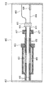
図2は、本実施形態における光トランシーバの、導波路構造を示す図である。この導波路構造を有する光トランシーバは、以下のように作成される。
まず、化合物半導体であるn−InP基板201上に、1.55Q組成i−InGaAsP活性層203を、予め有機金属気相成長法(metal organic chemical vapor deposition:MOCVD)により成長させる。次いでSOA領域の活性層を残してその他の領域を、ドライエッチングとウエットエッチングにより活性層の下まで除去し、MOCVD法の選択成長を利用して、パッシブ領域の1.4Q組成i−InGaAsPコア層203を成長させる。続いて電子線リソグラフィおよびウエットエッチングにより、周期約240nmのグレーティングパタンを1.4Q組成i−InGaAsPコア層203上に形成する。さらにMOCVD法によりSOAの領域、およびグレーティングを含むマッハツェンダ干渉計の導波路領域を含む基板全面にp−InP層205を成長させる。さらにフォトリソグラフィとドライエッチングによりSOA、およびグレーティングを含むマッハツェンダ干渉計の導波路ストライプパタンを形成し、最後にMOCVD法によりFeドープ半絶縁性InP(semi-insulating InP:SI−InP)204によって埋め込み成長させることで、図2に示す導波路構造を作製する。導波路形成プロセス後、SOAとマッハツェンダ干渉計のグレーティング部分とに電流注入用のAu電極をそれぞれ形成する。また、第1のMMIカプラ101とグレーティング109、110との間に位置する導波路103、104の直上に、長さ100μmの屈折率制御用電極115を形成する。最後に劈開により本素子を切り出し、蒸着によりHR/ARコートを形成する。
FIG. 2 is a diagram showing a waveguide structure of the optical transceiver in the present embodiment. An optical transceiver having this waveguide structure is produced as follows.
First, a 1.55Q composition i-InGaAsP
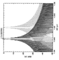
図3は、本実施形態における光トランシーバの、フィルタ動作時の透過特性を示す。2つのSOAにおける電流をOFF状態とし、導波路105から光を入力すると、導波路106からフィルタ選択光が出力される。2つのグレーティング109、110が形成されたアーム導波路103、104に電流注入し、プラズマ効果によりそのコア層の屈折率を0.3%減少させると、約4.5nm、中心波長が変化する。これは、光トランシーバが波長可変フィルタとして動作していることを表す。
FIG. 3 shows the transmission characteristics of the optical transceiver in this embodiment during the filter operation. When the currents in the two SOAs are turned off and light is input from the
さらに、第1のSOA113に電流を100mA程流すと、導波路105からレーザ発振光が出射される。また、グレーティング部分に電流注入すると、フィルタ動作時の場合と同様にグレーティングの反射特性が短波長側にシフトするに伴ってレーザ発振波長が変化する。これは、本光トランシーバが、波長可変レーザとして動作することを示す。さらに、屈折率制御用電極115の一方に電流注入すると、出射されるレーザ発振光が導波路105から導波路106に切り替わる。これは、アーム導波路103、104を伝搬する光の位相がπ変化したためである。この効果はフィルタ動作時の場合にも同様であり、導波路106から出力される選択光を、導波路105から出力されるように切り替えることも可能である。つまりこれは、フィルタ動作時およびレーザ動作時の出力導波路が、電気的に任意選択可能であることを意味し、例えばこの効果により、本光トランシーバの入出力に必要な光ファイバは最少1本で構成することができ、実装コストの削減とシステムの部品点数の削減に寄与することができる。
Further, when a current of about 100 mA is passed through the
本実施形態では、導波路ストライプパタン幅206を1.0μm、SOAの長さを600μm、グレーティングの長さを1500μm、グレーティングの深さDgを50nm、周期を240nmとして光トランシーバを作製した。この各数値は、本光トランシーバの特性を決める重要なパラメータとなる。
In the present embodiment, 1.0 .mu.m waveguide
波長可変光トランシーバを実現するにあたり、下記の条件が満たされることが好ましい。
1)導波路のコア層の高さ及び幅は、光が導波路をシングルモードで伝搬する条件が好ましく、本実施形態では0.1μm〜3.0μmである。
2)SOAの長さは、利得の大きさ、利得帯域幅、および飽和利得特性を決定し、本実施形態では20μm〜2000μmである。
3)グレーティングの長さは、フィルタ動作時の光強度損失、透過帯域幅、およびレーザ発振時の波長選択性能を決定し、本実施形態では50μm〜4000μmである。
4)グレーティングの振幅Dgは、グレーティングの結合係数を決定し、フィルタ動作時の透過帯域幅やレーザ発振時の波長選択性能に影響を与える。本実施形態では0.01μm〜2.0μmである。
5)周期は、光トランシーバの使用波長帯を決定し、本実施形態では中心波長を1.55μmとして、240nmである。
In realizing the wavelength tunable optical transceiver, it is preferable that the following conditions are satisfied.
1) The height and width of the core layer of the waveguide are preferably such that light propagates through the waveguide in a single mode, and in this embodiment, the height and width are 0.1 μm to 3.0 μm.
2) The length of the SOA determines the magnitude of gain, gain bandwidth, and saturation gain characteristics, and is 20 μm to 2000 μm in this embodiment.
3) The length of the grating determines the light intensity loss during the filter operation, the transmission bandwidth, and the wavelength selection performance during laser oscillation, and is 50 μm to 4000 μm in the present embodiment.
4) the amplitude D g of the grating determines the coupling coefficient of the grating, influence the wavelength selection performance in transmission bandwidth and the laser oscillation during the filter operation. In the present embodiment, it is 0.01 μm to 2.0 μm.
5) The period determines the wavelength band used for the optical transceiver, and in this embodiment, the center wavelength is 1.55 μm and is 240 nm.
また、本実施形態では、HRコートを施された端面を反射鏡として機能させて共振器を構成したが、HRコートを施された端面をグレーティングに置き換えてレーザ共振器を構成することも可能である。その場合、両端面にはARコートを施せば良い。また、利得媒質として1.55Q組成i−InGaAsP活性層を用いているが、活性層に多重量子井戸構造、あるいは歪み多重量子井戸構造を用いて利得帯域の拡大を図ることや、TE偏光あるいはTM偏光に利得を片寄らせて利得を増大させることも可能である。さらに、導波路を形成するためにFeドープ半絶縁性InPを用いているが、電流をブロックする他の系、例えば活性層に対し逆向きにInPのp−n接合を形成するp−n埋め込み構造(サイリスタ構造)を用いてもよい。また、光トランシーバを実現する導波路構造を埋め込み構造としているが、埋め込み構造以外の構造、例えばハイメサ構造やリッジ構造としてもよい。 Further, in this embodiment, the resonator is configured by functioning the end surface coated with HR as a reflecting mirror, but it is also possible to configure the laser resonator by replacing the end surface coated with HR with a grating. is there. In that case, AR coating may be applied to both end faces. Further, although a 1.55Q composition i-InGaAsP active layer is used as a gain medium, a gain band can be expanded by using a multiple quantum well structure or a strained multiple quantum well structure for the active layer, TE polarization or TM It is also possible to increase the gain by offsetting the gain to the polarization. In addition, Fe doped semi-insulating InP is used to form the waveguide, but other systems that block current, for example, pn buried that forms InP pn junctions in the opposite direction to the active layer. A structure (thyristor structure) may be used. The waveguide structure for realizing the optical transceiver is a buried structure, but a structure other than the buried structure, for example, a high mesa structure or a ridge structure may be used.
(第2の実施形態)
図4に、本発明の一実施形態による、第2の波長可変光トランシーバ400の構造図を示す。本実施形態ではマッハツェンダ干渉計を用いた構成ではなく、1つのMMIカプラ401を2入力2出力型光結合器として用いた構成となっている。すなわち、第1の実施形態と比較して、グレーティングと端面との間に位置する光結合器が1つ削減され、短共振器化が実現されている。これにより素子の縦モード間隔が広がり、レーザ動作時の発振波長が安定化される。また第1の実施形態では、反射鏡としてHRコートが施された端面を用いていたが、本実施形態では、両端面にARコート412が施され、同構造ではあるが、長さが200μmだけ長いグレーティング402が配置されて、レーザ共振器が構成されている。長さの異なるグレーティングを用いる理由は、共振器を構成するグレーティング間で反射率を異ならせ、レーザ発振光を導波路403、404側に出力させるためである。さらに第1の実施形態と同様に、MMIカプラ401とグレーティング402との間に位置する導波路405、406の直上に、長さ100μmの出力導波路を切り替えるための屈折率制御用電極407が形成され、グレーティング402の直上に、波長を変化させるための屈折率制御用電極411が形成されている。また、導波路404に光検出器(photodiode:PD)408が配置されている。このPD408は、利得媒質として用いているSOAと等しい層構造、導波路構造によって実現することができ、最適な逆バイアスを印加すればよい。
(Second Embodiment)
FIG. 4 shows a structural diagram of a second tunable
フィルタ動作時において、第1の実施形態と同様に波長多重された入力光は、導波路403に入射する。入射した入力光は、MMIカプラ401により導波路405、406に等しく分岐される。等分岐された入力光は、MMIカプラ401の出力導波路に配置されたグレーティング402により選択光のみが反射され、再びMMIカプラ401に入射する。選択光以外の光(非選択光)はグレーティング402を透過し、電流がOFF状態である第1のSOA409および第2のSOA410に入射し、吸収される。反射された選択光は、第1の実施形態と同様に導波路404に入射し、PD408によって光/電気変換が行われる。選択光が導波路404に入射しているときに、PD408に順方向バイアスを印加すると、PD408は利得媒質(SOA)として動作し、選択光を増幅することも可能である。さらに、屈折率制御用電極407に電流を注入し、光の位相をπ変化させると、導波路403に選択光を出力させることも可能である。
During the filter operation, the wavelength-multiplexed input light is incident on the
レーザ動作時には、第1のSOA409に電流を100mA程流すと、導波路403および導波路404からレーザ発振光が出射する。このとき、導波路403および導波路404から出力される光強度は等しいので、導波路404に配置されたPD408に流れる光電流により、導波路403から出力される光強度をモニタすることが可能である。さらに、共振器を構成する2つのグレーティング部分に電流注入すると、フィルタ動作時と同様にグレーティングの反射特性が短波長側にシフトするのに伴って、レーザ発振波長が変化する。これは、本光トランシーバが、波長可変レーザとして動作することを示す。
During laser operation, laser current is emitted from the
(第3の実施形態)
図5に、本発明の一実施形態による、第3の波長可変光トランシーバ500の構造図を示す。
(Third embodiment)
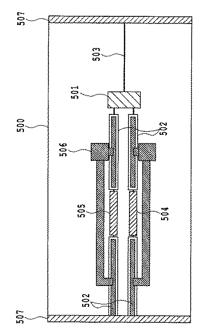
FIG. 5 shows a structural diagram of a third tunable
第2の実施形態における光トランシーバ400は、光結合器として2入力2出力型光結合器を用いた構成となっているが、本実施形態における光トランシーバ500は、1つのMMIカプラ501として1入力2出力型光結合器を用いて構成される。したがって、本実施形態では、入出力導波路は1本のみとなる。
The
符号502はグレーティングを、符号503は導波路を、符号504は第1のSOAを、符号505は第2のSOAを、符号506は波長を変化させるための屈折率制御用電極を、符合507はARコートを表し、それぞれ、第2の実施形態と同様に構成されている。
また、第2の実施形態と同様に、第1の実施形態と比較して、グレーティングと端面との間に位置する光結合器が1つ削減され、短共振器化が実現されている。これにより素子の縦モード間隔が広がり、レーザ動作時の発振波長が安定化される。 Similarly to the second embodiment, one optical coupler positioned between the grating and the end face is reduced as compared with the first embodiment, and a short resonator is realized. Thereby, the longitudinal mode interval of the element is widened, and the oscillation wavelength during laser operation is stabilized.
本実施形態における光トランシーバの作製方法、および導波路構造は、第1の実施形態と同様である。 The manufacturing method of the optical transceiver and the waveguide structure in the present embodiment are the same as those in the first embodiment.
(第4の実施形態)
図6に、本発明の一実施形態による、第4の波長可変光トランシーバ600の構造図を示す。本実施形態における光トランシーバ600は、2入力1出力型光結合器として1つのMMIカプラ601を用いた構成となっている。この構成により、第2の実施形態の場合と同様に、短共振器化によるレーザ発振波長の安定化が可能となる。さらに、屈折率制御用電極602が波長可変用の1つのみであるため、本光トランシーバを制御する電気回路作製の、大幅な低コスト化が可能となる。
(Fourth embodiment)
FIG. 6 shows a structural diagram of a fourth tunable
フィルタ動作時において、第2の実施形態の場合と同様に波長多重された入力光は、ARコート603側の導波路604に入射する。入射した入力光はMMIカプラ601を通過し、MMIカプラ601の出力導波路606に配置されたグレーティング607により選択光のみが反射され、再びMMIカプラ601に入射する。選択光以外の光(非選択光)はグレーティング606を透過し、電流がOFF状態であるSOA608に入射し、HRコート610を施した端面で反射されることなく吸収される。反射された選択光は、導波路604および導波路605から等しく出力される。出力される光強度は等しいので、導波路605に配置されたPD609に流れる光電流により、導波路604から出力される光強度をモニタすることが可能である。さらに、グレーティング部分に電流注入すると、フィルタ動作時と同様にグレーティング607の反射特性が短波長側にシフトする。
During the filter operation, the input light wavelength-multiplexed as in the second embodiment is incident on the
レーザ動作時には、SOA608に電流を100mA程流すと、導波路604および導波路605からレーザ発振光が出射される。このとき、導波路604および導波路605から出力される光強度は等しいので、フィルタ動作時と同様にPD609に流れる光電流により、導波路604から出力される光強度をモニタすることが可能である。
During laser operation, laser current is emitted from the
本実施形態における光トランシーバの作製方法、および導波路構造は、第1の実施形態および第2の実施形態と同様である。 The manufacturing method of the optical transceiver and the waveguide structure in this embodiment are the same as those in the first embodiment and the second embodiment.
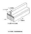
(第5の実施形態)
図7に、本発明の一実施形態による、波長可変光トランシーバのグレーティング構造図を示す。本実施形態では、化合物半導体であるn−InP基板上に、1.55Q組成i−InGaAsP活性層、およびp−InP上部クラッド層を、予めMOCVD法により成長させる。次いでSOA領域を残してその他の領域を、ドライエッチングとウエットエッチングにより活性層の下まで除去し、MOCVD法の選択成長を利用して、パッシブ領域の1.4Q組成i−InGaAsPコア層およびp−InP上部クラッド層を一括成長させる。次にプラズマCVD法により基板にSiO2を堆積させ、電子線リソグラフィとドライエッチングにより、図7(a)に示すSiO2グレーティングパタンを形成する。さらにそれをマスクとして使用し、図7(b)に示す、側壁に1次のグレーティングを持つハイメサ光導波路を作製する。導波路作製行程の最後に、フォトリソグラフィとドライエッチングとにより、図8に示すSOAの導波路構造であるリッジ構造を作製する。
(Fifth embodiment)
FIG. 7 shows a grating structure diagram of a wavelength tunable optical transceiver according to an embodiment of the present invention. In the present embodiment, a 1.55Q composition i-InGaAsP active layer and a p-InP upper cladding layer are grown in advance by MOCVD on an n-InP substrate that is a compound semiconductor. Next, the other regions except the SOA region are removed to the bottom of the active layer by dry etching and wet etching, and the 1.4Q composition i-InGaAsP core layer and the p- The InP upper clad layer is grown at once. Next, SiO 2 is deposited on the substrate by plasma CVD, and an SiO 2 grating pattern shown in FIG. 7A is formed by electron beam lithography and dry etching. Further, using this as a mask, a high mesa optical waveguide having a primary grating on the side wall as shown in FIG. At the end of the waveguide fabrication process, a ridge structure, which is the SOA waveguide structure shown in FIG. 8, is fabricated by photolithography and dry etching.
ハイメサ導波路の側壁にグレーティングが形成された構造を用いたのは、埋め込み型グレーティングでは不可能である、グレーティングの振幅を変調することを可能とし、フィルタの透過特性を所望の特性に合成することが目的である。一般に埋め込み型グレーティングを形成する場合、基板の深さ方向にエッチングし、グレーティングを形成する。しかし上記合成を行う場合には、グレーティングの振幅を変調する、つまりエッチング深さに面内分布をつける必要があり、作製上非常に困難である。そこで、ハイメサ導波路の側壁にグレーティングを形成した構造を用いることにより、電子線リソグラフィの導波路形成パタンを調整し、そのマスクパタンを用いてハイメサ導波路を形成することによって、グレーティングの振幅が変調できるようになる。 Using a structure in which a grating is formed on the side wall of a high-mesa waveguide makes it possible to modulate the amplitude of the grating, which is impossible with an embedded grating, and to combine the transmission characteristics of the filter with the desired characteristics. Is the purpose. In general, when forming an embedded grating, etching is performed in the depth direction of the substrate to form the grating. However, when the above synthesis is performed, it is necessary to modulate the amplitude of the grating, that is, to give an in-plane distribution to the etching depth, which is very difficult in production. Therefore, by using a structure in which a grating is formed on the side wall of the high mesa waveguide, the waveguide formation pattern of electron beam lithography is adjusted, and the high mesa waveguide is formed using the mask pattern, thereby modulating the amplitude of the grating. become able to.
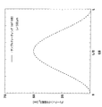
本実施形態では、図7(a)に示すグレーティングの深さDgを、正弦関数(変数が0〜π)の2乗で変調する。これにより、グレーティングの結合係数は、フィルタの中央部で最大になり、かつ周辺部において中央から遠ざかるにしたがって小さくなるように変調される。グレーティングの全長Lに対するグレーティングの振幅Dgの分布を図9に、作製した光トランシーバの透過特性を図10に示す。グレーティングの全長Lは、1500μmである。図10には、グレーティングの振幅を変調しないで均一分布で作製した光トランシーバの透過特性を同時に示している。図10から明らかなように、均一分布ではサイドロープ消光比は8dB程度であるが、グレーティングの結合係数を正弦関数的な分布にすることによって、波長多重光伝送に用いられる波長フィルタに必要な30dB以上のサイドロープ消光比が得られる。さらに、この導波路側壁にグレーティングが形成された構造を採用することにより、歩留まり低下および高コスト化をもたらしていたMOCVD法によるグレーティングを埋め込む工程が、不要となる。 In the present embodiment, the depth D g of the grating shown in FIG. 7 (a), a sine function (variable 0~Pai) modulated by the square of. As a result, the coupling coefficient of the grating is modulated so that it becomes maximum at the center of the filter and becomes smaller as it goes away from the center at the periphery. A grating distribution of amplitudes D g of of the total length L of the grating in Figure 9 shows the transmission characteristic of the optical transceiver manufactured in FIG. The overall length L of the grating is 1500 μm. FIG. 10 simultaneously shows the transmission characteristics of an optical transceiver manufactured with a uniform distribution without modulating the amplitude of the grating. As is clear from FIG. 10, the side rope extinction ratio is about 8 dB in the uniform distribution, but by making the coupling coefficient of the grating a sinusoidal distribution, 30 dB required for the wavelength filter used for wavelength division multiplexing optical transmission. The above side rope extinction ratio can be obtained. Further, by adopting the structure in which the grating is formed on the side wall of the waveguide, the step of embedding the grating by the MOCVD method, which has caused the yield reduction and the cost increase, becomes unnecessary.
本実施形態では、ハイメサ導波路幅を1.0μm、SOAのリッジ導波路幅を2.0μm、SOAの長さを600μm、グレーティングの長さを1500μm、グレーティングの深さDgの最大値を50nm、周期を240nmとして光トランシーバを作製した。この各数値は、本光トランシーバの特性を決める重要なパラメータとなる。波長可変光トランシーバを実現するにあたり、下記の条件が満たされることが好ましい。
1)導波路のコア層の高さ及び幅は、光が導波路をシングルモードで伝搬する条件が好ましく、本実施形態では0.1μm〜3.0μmである。
2)SOAの長さは、利得の大きさ、利得帯域幅、および飽和利得特性に影響を与え、本実施形態では20μm〜2000μmである。
3)グレーティングの長さは、フィルタ動作時の光強度損失、透過帯域幅、およびレーザ発振時の波長選択性能を決定し、本実施形態では50μm〜4000μmである。
4)グレーティングの振幅Dgは、グレーティングの結合係数を決定し、フィルタ動作時の透過帯域幅やレーザ発振時の波長選択性能を決める。本実施形態では0μm〜3.0μmである。
5)周期Λは、光トランシーバの使用波長帯を決定し、本実施形態では中心波長を1.55μmとして、240nmである。
In the present embodiment, the high-mesa waveguide width of 1.0 .mu.m, 2.0 .mu.m of SOA ridge waveguide width, 600 .mu.m and the length of the SOA, 1500 .mu.m length of the grating, 50 nm the maximum grating depth D g The optical transceiver was fabricated with a period of 240 nm. Each numerical value is an important parameter that determines the characteristics of the present optical transceiver. In realizing the wavelength tunable optical transceiver, it is preferable that the following conditions are satisfied.
1) The height and width of the core layer of the waveguide are preferably such that light propagates through the waveguide in a single mode, and in this embodiment, the height and width are 0.1 μm to 3.0 μm.
2) The length of the SOA affects the magnitude of gain, gain bandwidth, and saturation gain characteristics, and is 20 μm to 2000 μm in this embodiment.
3) The length of the grating determines the light intensity loss during the filter operation, the transmission bandwidth, and the wavelength selection performance during laser oscillation, and is 50 μm to 4000 μm in the present embodiment.
4) the amplitude D g of the grating determines the coupling coefficient of the grating determines the transmission bandwidth and wavelength selection performance in the laser oscillation during the filter operation. In this embodiment, it is 0 μm to 3.0 μm.
5) The period Λ determines the wavelength band used for the optical transceiver, and in this embodiment, the center wavelength is 1.55 μm and is 240 nm.
また、本実施形態では、グレーティングの導波路構造をハイメサ構造として作製したが、ハイメサ構造以外の構造、例えば図8に示すリッジ型構造において、リッジの側壁にグレーティングが形成された構造として作製してもよい。 In the present embodiment, the waveguide structure of the grating is manufactured as a high mesa structure. However, in the structure other than the high mesa structure, for example, in the ridge type structure shown in FIG. Also good.
(第6の実施形態)
図11に、本発明の一実施形態による、第5の波長可変光トランシーバ1100の構造を示す。本実施形態における光トランシーバ1100は、第1の実施形態におけるグレーティングおよび屈折率制御用電極が形成されたマッハツェンダ干渉計がちょうど向かい合うように、互いの導波路が接続され、その接続された導波路の間にSOA1101が配置された構成になっている。さらに両端面にはARコート1102が形成されている。
(Sixth embodiment)
FIG. 11 shows the structure of a fifth tunable
本実施形態では、複数の反射ピークを持つ第1のサンプルドグレーティング1103、および第2のサンプルドグレーティング1104が、マッハツェンダ干渉計のアームにそれぞれ形成されている。さらに第1のサンプルドグレーティング1103と第2のサンプルドグレーティング1104との間で、反射ピーク間隔をわずかに異ならせている。そのため出力が得られるのは反射ピークが一致した波長となり、素子全体の反射ピーク間隔は第1のサンプルドグレーティング1103と第2のサンプルドグレーティング1104との最小公倍数となる。さらに第1のサンプルドグレーティング1103と第2のサンプルドグレーティング1104が形成された導波路の屈折率を電流注入によりわずかに変化させると、バーニア目盛りのように一致するピークが大きくシフトし、波長可変域を増大させることが可能となる。 In the present embodiment, a first sampled grating 1103 and a second sampled grating 1104 having a plurality of reflection peaks are respectively formed on the arms of the Mach-Zehnder interferometer. Further, the reflection peak interval is slightly different between the first sampled grating 1103 and the second sampled grating 1104. Therefore, the output is obtained at the wavelength where the reflection peaks coincide, and the reflection peak interval of the entire element is the least common multiple of the first sampled grating 1103 and the second sampled grating 1104. Furthermore, if the refractive index of the waveguide in which the first sampled grating 1103 and the second sampled grating 1104 are formed is slightly changed by current injection, the matching peak like a vernier scale is greatly shifted, and the wavelength is variable. The area can be increased.
フィルタ動作時において、波長多重された入力光は、導波路1105に入射する。入射した入力光はまず、第1のMMIカプラ1107により両アームに等しく分岐される。等分岐された入力光は、アームに配置された第1のサンプルドグレーティング1103により選択光のみが反射され、再び第1のMMIカプラ1107に入射する。選択光以外の光(非選択光)は、第1のサンプルドグレーティング1103を透過する。両アームに形成されたサンプルドグレーティング1103は構造が同じなので、反射光(選択光)および透過光(非選択光)は位相差を保持したまま、それぞれ第2のMMIカプラ1108に入射する。ゆえに選択光は、SOA1101が配置された導波路1111を通過し、さらに後段のマッハツェンダ干渉計に入射する。非選択光は、ARコートが形成された入射端面とは反対側の端面を通過して、素子の外に放出される。
During the filter operation, the wavelength-multiplexed input light enters the
本実施形態では、SOA1101における電流を、フィルタ動作時およびレーザ動作時ともに常にONとし、フィルタ動作時において前段のマッハツェンダ干渉計によって選択された信号光を増幅する。したがって、後段のマッハツェンダ干渉計にさらに入射し、さらにそのマッハツェンダ干渉計によって選択された信号光は、導波路1106に出力される。レーザ動作とフィルタ動作との切り替えを、MMIカプラとサンプルドグレーティングの間に位置するアーム導波路の直上に形成した屈折率制御用電極1112、1113に電流注入することにより行うということが、本実施形態における光トランシーバの最大の特徴である。この構成により、フィルタ動作時にも光信号を利得媒質を用いて増幅することが可能となる。
In the present embodiment, the current in the
レーザ動作時においても、SOA1101における電流をONとし、SOA1101を利得媒質として機能させるということは、フィルタ動作時と同様である。本実施形態では、前段および後段のマッハツェンダ干渉計のアームに形成された屈折率制御用電極1114の一方に電流注入を行い、光の位相をπ変化させることができる。そうすることにより、前段および後段のマッハツェンダ干渉計に形成された第1のサンプルドグレーティング1103と第2のサンプルドグレーティング1104との間で帰還作用が働き、両者によってレーザ発振に不可欠な共振器が構成される。したがって、その状態でSOAの利得が素子のもつ光強度損失を越えると、レーザ発振に至る。レーザ発振光の波長は、両サンプルドグレーティングにおける反射率の積が最も高くなる波長で決まり、導波路1105および導波路1104からレーザ発振光が各々出力される。
Even during the laser operation, the current in the
本実施形態における光トランシーバの作製方法、および導波路構造は、第5の実施形態と同様である。ただし、サンプルドグレーティングは、グレーティングが存在するところと存在しないところが光の伝搬方向に対して周期的に繰り返した構造をとる。この場合のグレーティングの全長Lに対するグレーティングの振幅Dgの分布の一例を、図12に示す。本実施形態では、サイドロープ消光比を向上させる目的でグレーティングの振幅Dgを、グレーティングの中央部で最大、かつ中央から遠ざかるにしたがって振幅が小さくなるように正弦関数(変数は0〜π)の2乗で変調する。 The manufacturing method of the optical transceiver and the waveguide structure in the present embodiment are the same as those in the fifth embodiment. However, the sampled grating has a structure in which the presence and absence of the grating are periodically repeated in the light propagation direction. An example of the distribution of the grating amplitude D g of the total length L of the grating in this case is shown in FIG. 12. In the present embodiment, for the purpose of improving the side rope extinction ratio, the amplitude Dg of the grating is maximized at the central portion of the grating, and the sinusoidal function (variable is 0 to π) so that the amplitude decreases as the distance from the center decreases. Modulate with square.
作製した光トランシーバの、フィルタ動作時の透過特性を図13に示す。このとき、SOAにおいて電流を100mA程注入し、入出力導波路1から光を入力すると、入出力導波路2からフィルタ選択光が出力される。図13には、ピーク間隔がそれぞれ3.2nmと4.0nmであるサンプルドグレーティングが形成された、マッハツェンダ干渉計単体の透過特性も示している。図13から、素子全体のピーク間隔は、サンプルドグレーティング1とサンプルドグレーティング2のピーク間隔の最小公倍数である16nmであることがわかる。さらにサンプルドグレーティング1および2が形成された導波路にそれぞれ適切に電流注入すると、波長1550nmを中心とする可変域16nmのすべての波長が選択可能である。すなわち、電流注入による屈折率変化量の最大値を大きく超える波長可変量が得られる。
FIG. 13 shows the transmission characteristics of the fabricated optical transceiver during filter operation. At this time, when a current of about 100 mA is injected into the SOA and light is input from the input /
レーザ動作時には、SOAに電流を100mA程流し、さらに屈折率制御用電極の一方に電流注入を行い、光の位相をπ変化させると、入出力導波路1および入出力導波路2からレーザ発振光が出射される。この場合に、入出力導波路1および入出力導波路2から出力される光強度は等しいので、入出力導波路2にPDに配置すれば、入出力導波路2を流れる光電流により入出力導波路1から出力される光強度をモニタすることが可能である。さらに、共振器を構成する前段および後段のマッハツェンダ干渉計のグレーティング部分に電流注入すると、フィルタ動作時と同様にグレーティングの反射特性が大きくシフトするに伴って、レーザ発振波長が変化する。これは、本光トランシーバが、広帯域波長可変レーザとしても動作することをあらわす。
During laser operation, if a current of about 100 mA is passed through the SOA, and current is injected into one of the refractive index control electrodes to change the phase of the light by π, the laser oscillation light from the input /
(第7の実施形態)
図14に、本発明の一実施形態による、波長可変光トランシーバのグレーティングの全長Lに対する、グレーティングの振幅Dgの分布を示す。本実施形態における光トランシーバは、第6の実施形態の場合と同様に、グレーティングおよび屈折率制御用電極が形成されたマッハツェンダ干渉計が向かい合うように互いの入出力導波路が接続され、その接続された入出力導波路の間にSOAが配置された構成になっている。さらに両端面にはARコートが形成されている。ただし、レーザ動作時における発振波長の安定化を目的として、グレーティングの振幅Dgを、以下の式で示すSinc関数、Sinc関数の逆数、および正弦関数の2乗の積で変調した。
(Seventh embodiment)
14 shows according to an embodiment of the present invention, of the total length L of the grating of the tunable optical transceiver, the distribution of the amplitude D g of the grating. As in the case of the sixth embodiment, the optical transceiver in this embodiment is connected to the input / output waveguides so that the Mach-Zehnder interferometers on which the grating and the refractive index control electrode are formed face each other. The SOA is arranged between the input / output waveguides. Furthermore, an AR coat is formed on both end faces. However, for the purpose of stabilization of the oscillation wavelength during laser operation, the amplitude D g of the grating was modulated by the square of the product of Sinc function, the inverse of Sinc function, and the sine function shown by the following equation.
Nは反射ピークの本数を表し、本実施形態では5である。Lはグレーティングの全長を表し、本実施形態では1500μmである。Pは反射ピーク間隔を決めるパラメータであり、次式から求まる。 N represents the number of reflection peaks, and is 5 in this embodiment. L represents the total length of the grating, which is 1500 μm in this embodiment. P is a parameter that determines the reflection peak interval, and is obtained from the following equation.
ここで、neffは実効屈折率を表し、本実施形態では3.8である。λBは中心波長を表し、本実施形態では1.55μmである。Δλは反射ピーク間隔を表し、図14では3.2nmである。 Here, n eff represents an effective refractive index and is 3.8 in the present embodiment. λ B represents the center wavelength, which is 1.55 μm in this embodiment. Δλ represents the reflection peak interval, which is 3.2 nm in FIG.
本実施形態における光トランシーバの、フィルタ動作時における透過特性を図15に示す。このとき、SOAにおいて電流を100mA程注入し、入出力導波路1から光を入力すると、入出力導波路2からフィルタ選択光が出力される。図15には、ピーク間隔がそれぞれ3.2nmと4.0nmであるマッハツェンダ干渉計単体の透過特性も示している。図13に示す透過特性を有する光トランシーバでは、サンプルドグレーティング1とサンプルドグレーティング2のピーク間隔の最小公倍数である16nmごとに、周期的な光出力が得られたが、本実施形態における光トランシーバは、上記変調関数により反射ピーク本数が5本のみに制限され、図15に示すように単一透過特性を有する。つまり、第6の実施形態における光トランシーバでは、周期的な波長間隔ごとに透過帯域が現れるため、この透過ピーク間隔がSOAの帯域幅より狭くなると、モードホップによる発振動作の不安定化が問題となる。しかしこの問題は、上記変調関数によって光トランシーバが単一透過特性を得ることにより解決される。
FIG. 15 shows the transmission characteristics of the optical transceiver in this embodiment during the filter operation. At this time, when a current of about 100 mA is injected into the SOA and light is input from the input /
最後に、各実施形態における光トランシーバには、InP系の化合物半導体を用いたが、光ファイバにグレーティングが形成されたファイバブラッググレーティング(fiber bragg grating)、および利得媒質としてエルビウム添加ファイバアンプ(erbium doped fiber amplifier)などを組み合わせても実現できる。さらにGaAs系導波路、Si/SiO2系のシリコン細線導波路、あるいはポリイミドなどで構成される導波路などでも同様に実現できる。 Finally, although an InP-based compound semiconductor is used for the optical transceiver in each embodiment, a fiber bragg grating in which a grating is formed in an optical fiber, and an erbium doped fiber amplifier (erbium doped) as a gain medium It can also be realized by combining a fiber amplifier). Further, a GaAs-based waveguide, a Si / SiO 2 -based silicon fine wire waveguide, or a waveguide made of polyimide or the like can be similarly realized.
また、各実施形態では、半導体導波路への電流注入による屈折率変化を用いたが、電圧、熱、または圧力を導波路に印加することによる屈折率変化を用いても、波長可変動作を得ることができるのは明らかである。 In each embodiment, the refractive index change due to current injection into the semiconductor waveguide is used. However, the wavelength variable operation can be obtained even when the refractive index change is applied by applying voltage, heat, or pressure to the waveguide. Obviously you can.
100 波長可変光トランシーバ
101、102 2入力2出力型MMIカプラ
103、104 アーム導波路
105、106、107、108 導波路
109、110 グレーティング
111 ARコート
112 HRコート
113、114 SOA
115、116 屈折率制御用電極
100 Wavelength
115, 116 Refractive index control electrode
Claims (12)
第1の2入力2出力型光結合器と、
第2の2入力2出力型光結合器と、
前記第1および第2の2入力2出力型光結合器のそれぞれにその両端が接続された2つのアーム導波路と、
前記第1の2入力2出力型光結合器にその一端が接続され、他端が前記光トランシーバのARコートが施された端面に接続された2つの導波路と、
前記第2の2入力2出力型光結合器にその一端が接続され、他端が前記光トランシーバのHRコートが施された端面に接続された2つの導波路と
を用いて構成されたマッハツェンダ干渉計と、
前記2つのアーム導波路に形成されたグレーティングと、
前記マッハツェンダ干渉計のHRコート側の2つの前記導波路に配置された利得媒質と
からなり、
前記利得媒質において利得と吸収とを選択する手段を有すること
を特徴とする光トランシーバ。 An optical transceiver having a laser operation and a filter operation,
A first two-input two-output optical coupler;
A second 2-input 2-output optical coupler;
Two arm waveguides connected at both ends to each of the first and second two-input two-output optical couplers;
Two waveguides having one end connected to the first two-input two-output optical coupler and the other end connected to an end surface of the optical transceiver on which an AR coating is applied;
Mach-Zehnder interference configured using two waveguides having one end connected to the second two-input two-output optical coupler and the other end connected to the end face of the optical transceiver on which the HR coating is applied. Total
A grating formed on the two arm waveguides;
The gain medium disposed in the two waveguides on the HR coat side of the Mach-Zehnder interferometer,
An optical transceiver comprising means for selecting gain and absorption in the gain medium.
1つの2入力2出力型光結合器と、
前記1つの2入力2出力型光結合器にその一端が接続され、他端が前記光トランシーバのARコートが施された端面に接続された4つの導波路と、
前記4つの導波路のうちの2つの導波路に形成されたグレーティングと、
前記グレーティングが形成された前記2つの導波路に配置された利得媒質と、
前記4つの導波路のうちの、前記グレーティングが形成されていない1つの導波路に配置された光検出器と
からなり、
前記利得媒質において利得と吸収とを選択する手段を有すること
を特徴とする光トランシーバ。 An optical transceiver having a laser operation and a filter operation,
One 2-input 2-output optical coupler;
Four waveguides having one end connected to the one two-input two-output optical coupler and the other end connected to an end surface of the optical transceiver on which an AR coating is applied;
A grating formed in two of the four waveguides;
A gain medium disposed in the two waveguides in which the grating is formed;
A photodetector arranged in one of the four waveguides where the grating is not formed;
An optical transceiver comprising means for selecting gain and absorption in the gain medium.
1つの1入力2出力型光結合器と、
前記1つの1入力2出力型光結合器にその一端が接続され、他端が前記光トランシーバのARコートが施された端面に接続された3つの導波路と、
前記3つの導波路のうちの2つの導波路に形成されたグレーティングと、
前記グレーティングが形成された前記2つの導波路に配置された利得媒質と
からなり、
前記利得媒質において利得と吸収とを選択する手段を有すること
を特徴とする光トランシーバ。 An optical transceiver having a laser operation and a filter operation,
One 1-input 2-output optical coupler;
Three waveguides having one end connected to the one-input two-output optical coupler and the other end connected to an end surface of the optical transceiver on which an AR coating is applied;
A grating formed in two of the three waveguides;
A gain medium disposed in the two waveguides in which the grating is formed,
An optical transceiver comprising means for selecting gain and absorption in the gain medium.
1つの2入力1出力型光結合器と、
前記1つの2入力1出力型光結合器にその一端が接続され、他端が前記光トランシーバのARコートが施された端面に接続された2つの導波路と、
前記1つの2入力1出力型光結合器にその一端が接続され、他端が前記光トランシーバのHRコートが施された端面に接続された1つの導波路と、
前記1つの2入力1出力型光結合器のHRコート側の導波路に形成されたグレーティングと、
前記グレーティングが形成された前記1つの導波路に配置された利得媒質と、
前記1つの2入力1出力型光結合器のARコート側の1つの導波路に配置された光検出器と
からなり、
前記利得媒質において利得と吸収とを選択する手段を有すること
を特徴とする光トランシーバ。 An optical transceiver having a laser operation and a filter operation,
One 2-input 1-output optical coupler;
Two waveguides having one end connected to the one two-input one-output optical coupler and the other end connected to an end face of the optical transceiver that has been coated with an AR coat;
One waveguide having one end connected to the one two-input one-output optical coupler and the other end connected to an end face of the optical transceiver on which HR coating is applied;
A grating formed in a waveguide on the HR coat side of the one two-input one-output optical coupler;
A gain medium disposed in the one waveguide in which the grating is formed;
A photodetector arranged in one waveguide on the AR coat side of the one two-input one-output optical coupler;
An optical transceiver comprising means for selecting gain and absorption in the gain medium.
12. The optical transceiver according to claim 1, wherein the refractive index control means changes the refractive index using one or more of a thermo-optic effect, current injection, electric field application, and pressure application. Optical transceiver.
Priority Applications (1)
| Application Number | Priority Date | Filing Date | Title |
|---|---|---|---|
| JP2006073299A JP2007248901A (en) | 2006-03-16 | 2006-03-16 | Optical transceiver |
Applications Claiming Priority (1)
| Application Number | Priority Date | Filing Date | Title |
|---|---|---|---|
| JP2006073299A JP2007248901A (en) | 2006-03-16 | 2006-03-16 | Optical transceiver |
Publications (1)
| Publication Number | Publication Date |
|---|---|
| JP2007248901A true JP2007248901A (en) | 2007-09-27 |
Family
ID=38593257
Family Applications (1)
| Application Number | Title | Priority Date | Filing Date |
|---|---|---|---|
| JP2006073299A Pending JP2007248901A (en) | 2006-03-16 | 2006-03-16 | Optical transceiver |
Country Status (1)
| Country | Link |
|---|---|
| JP (1) | JP2007248901A (en) |
Cited By (2)
| Publication number | Priority date | Publication date | Assignee | Title |
|---|---|---|---|---|
| JP2010050135A (en) * | 2008-08-19 | 2010-03-04 | Nec Corp | Semiconductor optical integrated device and optical communication apparatus |
| CN104949938A (en) * | 2015-06-16 | 2015-09-30 | 电子科技大学 | Mach-Zehnder modulation type resonant cavity sensor based on vernier effect |
-
2006
- 2006-03-16 JP JP2006073299A patent/JP2007248901A/en active Pending
Cited By (2)
| Publication number | Priority date | Publication date | Assignee | Title |
|---|---|---|---|---|
| JP2010050135A (en) * | 2008-08-19 | 2010-03-04 | Nec Corp | Semiconductor optical integrated device and optical communication apparatus |
| CN104949938A (en) * | 2015-06-16 | 2015-09-30 | 电子科技大学 | Mach-Zehnder modulation type resonant cavity sensor based on vernier effect |
Similar Documents
| Publication | Publication Date | Title |
|---|---|---|
| JP6540214B2 (en) | Multi-wavelength laser light source and wavelength multiplex communication system | |
| JP3323725B2 (en) | Polarization modulation laser, driving method thereof, and optical communication system using the same | |
| KR100916311B1 (en) | The wavelength tunable laser diode using double coupled ring resonator | |
| US7158547B2 (en) | Wavelength tunable laser of small size | |
| JP2016178283A (en) | Wavelength variable laser element and laser module | |
| JP3985159B2 (en) | Gain clamp type semiconductor optical amplifier | |
| JP2017098362A (en) | Optical integrated device and optical communication device | |
| JP2017219668A (en) | Wavelength variable light source | |
| JP2017216384A (en) | Tunable laser | |
| JPWO2013145271A1 (en) | Optical element, optical transmitter element, optical receiver element, hybrid laser, optical transmitter | |
| JP4906185B2 (en) | Optical semiconductor device and optical semiconductor device modulation method | |
| JP2008544530A (en) | Integrated monitoring and feedback design of external cavity tunable lasers | |
| JP6425631B2 (en) | Semiconductor laser and optical integrated light source having the same | |
| JP6337960B2 (en) | Optical transceiver module | |
| US20140254617A1 (en) | Tunable laser diode device with amzi-fp filter | |
| JP4648647B2 (en) | Tunable semiconductor laser | |
| US7382817B2 (en) | V-coupled-cavity semiconductor laser | |
| US6693937B2 (en) | Integrated tunable laser | |
| JPWO2008107975A1 (en) | Semiconductor integrated device | |
| JP5001239B2 (en) | Semiconductor tunable laser | |
| JP2018060974A (en) | Semiconductor optical integrated element | |
| JP4022792B2 (en) | Semiconductor optical amplifier | |
| JPH08334796A (en) | Optical wavelength conversion integrating element | |
| JP2007248901A (en) | Optical transceiver | |
| US20050226283A1 (en) | Single-mode semiconductor laser with integrated optical waveguide filter |