JP3870214B2 - Correction circuit - Google Patents
Correction circuit Download PDFInfo
- Publication number
- JP3870214B2 JP3870214B2 JP2005165552A JP2005165552A JP3870214B2 JP 3870214 B2 JP3870214 B2 JP 3870214B2 JP 2005165552 A JP2005165552 A JP 2005165552A JP 2005165552 A JP2005165552 A JP 2005165552A JP 3870214 B2 JP3870214 B2 JP 3870214B2
- Authority
- JP
- Japan
- Prior art keywords
- pixel
- memory
- predetermined
- correction
- screen
- Prior art date
- Legal status (The legal status is an assumption and is not a legal conclusion. Google has not performed a legal analysis and makes no representation as to the accuracy of the status listed.)
- Expired - Fee Related
Links
Images


Classifications
-
- G—PHYSICS
- G09—EDUCATION; CRYPTOGRAPHY; DISPLAY; ADVERTISING; SEALS
- G09G—ARRANGEMENTS OR CIRCUITS FOR CONTROL OF INDICATING DEVICES USING STATIC MEANS TO PRESENT VARIABLE INFORMATION
- G09G3/00—Control arrangements or circuits, of interest only in connection with visual indicators other than cathode-ray tubes
- G09G3/20—Control arrangements or circuits, of interest only in connection with visual indicators other than cathode-ray tubes for presentation of an assembly of a number of characters, e.g. a page, by composing the assembly by combination of individual elements arranged in a matrix no fixed position being assigned to or needed to be assigned to the individual characters or partial characters
- G09G3/22—Control arrangements or circuits, of interest only in connection with visual indicators other than cathode-ray tubes for presentation of an assembly of a number of characters, e.g. a page, by composing the assembly by combination of individual elements arranged in a matrix no fixed position being assigned to or needed to be assigned to the individual characters or partial characters using controlled light sources
-
- G—PHYSICS
- G09—EDUCATION; CRYPTOGRAPHY; DISPLAY; ADVERTISING; SEALS
- G09G—ARRANGEMENTS OR CIRCUITS FOR CONTROL OF INDICATING DEVICES USING STATIC MEANS TO PRESENT VARIABLE INFORMATION
- G09G2320/00—Control of display operating conditions
- G09G2320/02—Improving the quality of display appearance
- G09G2320/0285—Improving the quality of display appearance using tables for spatial correction of display data
-
- G—PHYSICS
- G09—EDUCATION; CRYPTOGRAPHY; DISPLAY; ADVERTISING; SEALS
- G09G—ARRANGEMENTS OR CIRCUITS FOR CONTROL OF INDICATING DEVICES USING STATIC MEANS TO PRESENT VARIABLE INFORMATION
- G09G3/00—Control arrangements or circuits, of interest only in connection with visual indicators other than cathode-ray tubes
- G09G3/20—Control arrangements or circuits, of interest only in connection with visual indicators other than cathode-ray tubes for presentation of an assembly of a number of characters, e.g. a page, by composing the assembly by combination of individual elements arranged in a matrix no fixed position being assigned to or needed to be assigned to the individual characters or partial characters
- G09G3/2007—Display of intermediate tones
- G09G3/2074—Display of intermediate tones using sub-pixels
Landscapes
- Engineering & Computer Science (AREA)
- Physics & Mathematics (AREA)
- Computer Hardware Design (AREA)
- General Physics & Mathematics (AREA)
- Theoretical Computer Science (AREA)
- Control Of Indicators Other Than Cathode Ray Tubes (AREA)
Description
本発明は、画像表示装置の駆動信号を補正する補正回路に関する。 The present invention relates to a correction circuit that corrects a drive signal of an image display device.
特許文献1には、電界放出ディスプレイにおけるスペーサの可視性を制御する方法として、スペーサ近傍の第1領域と、スペーサ非近傍の第2領域に領域を定義し、スペーサを視者に対して見えなくするために、スペーサ近傍の第1領域の複数画素によって発生する光の強度レベルに応じて第1領域に伝送する画素データを修正するという画素データ補正方法が開示されている。
しかしながら、n画素×nラインの複数画素に及ぶ影響範囲を考量し補正するケースにおいては、補正値を求めるために多くのメモリ量が必要となり、コストアップしてしまうものであった。 However, in the case where the range of influence over a plurality of pixels of n pixels × n lines is considered and corrected, a large amount of memory is required to obtain a correction value, resulting in an increase in cost.
そこで、本発明は、補正性能を低下させることなく、少ないメモリ量で補正値を求め、それにより補正回路のコスト低減可能な構成を実現することを目的とする。 In view of the above, an object of the present invention is to obtain a correction value with a small memory amount without degrading the correction performance, thereby realizing a configuration capable of reducing the cost of the correction circuit.
上記目的を達成するために本発明にあっては、以下の構成を採用する。すなわち、
画素信号を補正する補正回路であって、
所定画面の所定画素の近傍に位置する複数の周辺画素に対応する画素信号として順次入力される複数の画素信号に対して間引き処理を行った信号を記憶する第1メモリと、
補正値を前記第1メモリからの出力に基づいて算出する算出回路と、
前記所定画面よりも後の画面において前記所定画素を形成するための画素信号であって前記第1メモリを経由していない画素信号を、前記所定画面に対応する前記補正値で補正できるように前記補正値を出力するタイミングを調整するための第2メモリと、
前記所定画面よりも後の画面において前記所定画素を形成するための前記画素信号であって前記第1メモリを経由していない前記画素信号を、前記所定画面に対応する前記補正値で補正する演算を行う演算回路と、
を有しており、
前記補正値は、前記複数の周辺画素による前記所定画素の表示階調への影響が、補正された画素信号に基づいて画像表示する表示パネルが有する遮蔽部材によって抑制された量に対応する補正を行うための補正値である補正回路である。
In order to achieve the above object, the present invention adopts the following configuration. That is,
A correction circuit for correcting a pixel signal,
A first memory for storing a signal obtained by performing a thinning process on a plurality of pixel signals sequentially input as pixel signals corresponding to a plurality of peripheral pixels located in the vicinity of a predetermined pixel on a predetermined screen;
A calculation circuit that calculates a correction value based on an output from the first memory;
The pixel signal for forming the predetermined pixel on the screen after the predetermined screen and not passing through the first memory can be corrected with the correction value corresponding to the predetermined screen. A second memory for adjusting the timing of outputting the correction value;
Computation for correcting the pixel signal for forming the predetermined pixel on a screen after the predetermined screen but not passing through the first memory with the correction value corresponding to the predetermined screen An arithmetic circuit for performing
Have
The correction value is a correction corresponding to an amount in which the influence of the plurality of peripheral pixels on the display gradation of the predetermined pixel is suppressed by the shielding member included in the display panel that displays an image based on the corrected pixel signal. It is a correction circuit which is a correction value for performing.
また、
画素信号を補正する補正回路であって、
所定画面の所定画素の近傍に位置する複数の周辺画素に対応する画素信号として順次入力される複数の画素信号に対して間引き処理を行った信号を記憶する第1メモリと、
前記複数の周辺画素による前記所定画素の表示階調への影響量を補正するための補正値を前記第1メモリからの出力に基づいて算出する算出回路と、
前記所定画面よりも後の画面において前記所定画素を形成するための画素信号であって前記第1メモリを経由していない画素信号を、前記所定画面に対応する前記補正値で補正できるように前記補正値を出力するタイミングを調整するための第2メモリと、
前記所定画面よりも後の画面において前記所定画素を形成するための前記画素信号であって前記第1メモリを経由していない前記画素信号を、前記所定画面に対応する前記補正値で補正する演算を行う演算回路と、
を有する補正回路である。
Also,
A correction circuit for correcting a pixel signal,
A first memory for storing a signal obtained by performing a thinning process on a plurality of pixel signals sequentially input as pixel signals corresponding to a plurality of peripheral pixels located in the vicinity of a predetermined pixel on a predetermined screen;
A calculation circuit for calculating a correction value for correcting an influence amount on the display gradation of the predetermined pixel by the plurality of peripheral pixels based on an output from the first memory;
The pixel signal for forming the predetermined pixel on the screen after the predetermined screen and not passing through the first memory can be corrected with the correction value corresponding to the predetermined screen. A second memory for adjusting the timing of outputting the correction value;
Computation for correcting the pixel signal for forming the predetermined pixel on a screen after the predetermined screen but not passing through the first memory with the correction value corresponding to the predetermined screen An arithmetic circuit for performing
Is a correction circuit.
本発明によると、補正性能を低下させることなく、少ないメモリ量で補正値を求め、それにより補正回路のコスト低減ができる。 According to the present invention, the correction value can be obtained with a small amount of memory without degrading the correction performance, thereby reducing the cost of the correction circuit.
以下に図面を参照して、この発明の最良な実施形態を例示的に詳しく説明する。ただし、この実施形態に記載されている構成部品の寸法、材質、形状、その相対配置などは、特に特定的な記載がない限りは、この発明の範囲をそれらのみに限定する趣旨のものではない。 Hereinafter, exemplary embodiments of the present invention will be described in detail with reference to the drawings. However, the dimensions, materials, shapes, relative arrangements, and the like of the component parts described in this embodiment are not intended to limit the scope of the present invention only to those unless otherwise specified. .
(テレビジョン装置の実施形態)
まず、図11を用いて本発明が適用されるテレビジョン装置について説明する。図11は、本発明に係るテレビジョン装置のブロック図である。テレビジョン装置は、セットトップボックス(STB)501と、画像表示装置502と、を備える。
(Embodiment of Television Device)
First, a television device to which the present invention is applied will be described with reference to FIG. FIG. 11 is a block diagram of a television apparatus according to the present invention. The television device includes a set top box (STB) 501 and an image display device 502.
セットトップボックス(STB)501は、チューナ503およびI/F部504を有する。チューナ503は、衛星放送や地上波等のテレビ信号、ネットワークを介したデータ放送等を受信し、復号化した映像データをI/F部504に出力する。I/F部504は、映像データを画像表示装置502の表示フォーマットに変換して画像表示装置502に映像データを出力する。
The set top box (STB) 501 includes a
画像表示装置502は、表示パネル20、制御回路505、駆動回路506及び本発明の補正回路(信号処理部)を有する。I/F部504からの映像信号と同期信号にデコードされた映像データ(画素信号)が補正回路に入力される。すなわち、図2の信号処理部10が図11のI/F部504に接続されており、I/F部504からの信号は図2の信号処理部10に入力される。
The image display device 502 includes the
また、画像表示装置502に含まれる制御回路505は、駆動回路506に画像データ及び各種制御信号を出力する。制御回路505は、一例として図2におけるPWMパルス制御部14や駆動電圧制御部15が挙げられる。駆動回路506は、入力された画像データに基づいて、表示パネル20に駆動信号を出力し、表示パネル20上にはテレビ映像が表示されることとなる。駆動回路506は、一例として図2における列配線スイッチ部16や行配線スイッチ部18が挙げられる。表示パネル20は、以下の実施形態ではSEDパネルを例に挙げる。
A
なお、チューナ503とI/F部504は、セットトップボックス(STB)501として画像表示装置502とは別の筐体に収められていてもよいし、また画像表示装置502と同一の筐体に収められていてもよい。
Note that the
(第1の実施形態)
本発明の第1の実施形態について説明する。本発明の画像表示装置は、SED表示装置、FED表示装置、液晶表示装置、プラズマ表示装置、有機EL表示装置などを包含しており、特に、SED表示装置やFED表示装置などの電子線表示装置では、自発光した輝点輝度によって周辺画素でハレーション発光が生じる可能性がある点から本発明が適用される好ましい形態である。
(First embodiment)
A first embodiment of the present invention will be described. The image display device of the present invention includes an SED display device, an FED display device, a liquid crystal display device, a plasma display device, an organic EL display device and the like, and in particular, an electron beam display device such as an SED display device or an FED display device. Then, since the halation light emission may occur in the peripheral pixels due to the brightness of the self-luminous bright spot, this is a preferred form to which the present invention is applied.
更に、プラズマ表示装置においても放電セル間の隔壁がない場合や隔壁構造が画素単位より大きくなった場合などは同様に周辺画素へハレーション(クロストーク)が生じる可能性がある点から本発明が適用される好ましい形態である。 Further, in the plasma display device, when there is no partition between discharge cells, or when the partition structure is larger than a pixel unit, the present invention is applied because there is a possibility that halation (crosstalk) may occur in peripheral pixels. Preferred form.
まず、図2を用いて実施形態の画像表示装置の構成を示す。20は表示パネルである。本実施形態では、薄型の真空容器内に、基板上に多数の電子源、例えば冷陰極素子等の電子放出素子を配列してなるマルチ電子源と、電子の照射により画像を形成する画像形成部材とを対向して備えたSEDパネルを用いた。電子放出素子が行方向配線電極と列方向配線電極により単純マトリクス状に配線されており、列/行電極バイアスにより選択された素子から放出される電子を高圧電圧により加速し、蛍光体に衝突させることで発光を得ている。SEDパネルの構成と製造法については、特開2000-250463号公報に詳
しく開示されている。
First, the configuration of the image display apparatus according to the embodiment will be described with reference to FIG.
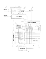
このSEDパネルに映像信号を入力し表示するまでの動作を説明する。信号S1は入力映像信号であり、信号処理部10にて、表示に好適な信号処理が成され、信号S2が表示信号として出力される。図2において信号処理部10の機能については、本実施形態を説明する上での必要最小限の機能ブロックについて記載している。
The operation until the video signal is input and displayed on the SED panel will be described. The signal S1 is an input video signal, signal processing suitable for display is performed in the
信号処理部10内の11は逆γ補正部である。一般的に、入力映像信号S1はCRTディスプレイ装置で表示することを前提として、CRTディスプレイの入力−発光特性に合わせたガンマ変換と呼ばれる0.45乗などの非線形変換が施されて伝送あるいは記録されている。その映像信号を、SED、FED、PDP、LCDなどの入力−発光特性が線形な表示デバイスに表示する場合には、入力信号に対して、2.2乗などの逆ガンマ変換を施す必要がある。また、逆γ補正部11への入力信号S1は各色8〜10ビットで入力されることが多いが、非線形な逆ガンマ変換による低階調部の黒つぶれなどを避ける為に、一般的に12ビット〜14ビットにデータ量を増やした変換がされることが多い。逆γ補正部11の出力データは表示パネルの輝度とデータが線形な系に変換され、本実施形態での特徴部分である補正回路としてのハレーション補正部12に入力する。ハレーション補正部12に関しては以降で詳しく説明する。
ハレーション補正部12からの出力は、SEDにとって最適な映像の表示信号S2として出力される。タイミング制御部13は、入力映像信号S1と共に受け渡された同期信号を元に、各ブロックの動作のための各種タイミング信号を生成し出力する。
The output from the
14はPWMパルス制御部で、水平1周期(行選択期間)毎に表示信号S2を表示パネル20に適応した駆動信号(例では、PWM変調)に変換する。15は駆動電圧制御部で、表示パネル20に配置されている素子を駆動する電圧を制御する。16は列配線スイッチ部で、トランジスタなどのスイッチ手段により構成され、毎水平1周期(行選択期間)ごとに駆動電圧制御部15からの駆動出力をPWMパルス制御部14から出力されるPWMパルス期間だけパネル列電極に印加する。17は行選択制御部で、表示パネル20上の素子を駆動する行選択パルスを発生する。18は行配線スイッチ部で、トランジスタなどのスイッチ手段により構成され、行選択制御部17から出力される行選択パルスに応じた駆動電圧制御部15の駆動出力を表示パネル20に出力する。19は高圧発生部で、表示パネル20に配置されている電子放出素子から放出された電子を蛍光体に衝突させるために加速する加速電圧を発生する。以上により、表示パネル20が駆動されて映像が表示される。
A PWM
次に、本発明の特徴部分であるハレーション補正部12について図面を参照して説明していく。
Next, the
ここで、図1のハレーション補正部12の説明に入る前にハレーション補正とは何かについて以下に説明する。
Here, before the description of the
本発明者は、図3(a)に示すように、リアプレートに形成した電子放出素子と、該電子放出素子と間隔を空けてフェースプレートに配置される発光体(本例では、赤、青、緑の各色の蛍光体)とを用い、電子放出素子から放出される電子ビーム(1次電子)を発光体に照射して発光体を発光させる画像表示装置において色再現性が所望の状態とは異なるという特有の課題が生じることを見出した。具体的な例を挙げると、青の蛍光体にのみ電子を照射して青色の発光を得ようとした場合に、純粋な青ではなく、わずかに他の色(緑と赤)の発光が混ざった発光状態、すなわち、彩度が良くない発光状態になることがわかった。本発明者は研究を重ねた結果、彩度が低下する原因は、電子放出素子が放出する1次電子が、該電子放出素子が対応する発光体に入射することで、対応する発光体が輝点発光するだけでなく、発光体で反射することで近接(隣接も含む)の異なる色の発光領域に反射電子(2次電子)として入射することで周辺の発光体も発光させることによって生じていることを確認した。この反射電子(2次電子)による発光を本明細書ではハレーションと呼んでいる。 As shown in FIG. 3A, the present inventor has an electron-emitting device formed on the rear plate and a light emitter (in this example, red, blue, and the like) disposed on the face plate at a distance from the electron-emitting device. The color reproducibility of the image display device in which the light emitter is irradiated by irradiating the light emitter with an electron beam (primary electrons) emitted from the electron-emitting device. I found that there is a unique problem that is different. As a specific example, when trying to obtain blue light emission by irradiating only the blue phosphor with electrons, the light emission of other colors (green and red) is slightly mixed instead of pure blue. It was found that the light emission state, that is, the light emission state with poor saturation was obtained. As a result of repeated studies by the present inventor, the cause of the decrease in saturation is that primary electrons emitted from the electron-emitting device are incident on the corresponding light-emitting body, so that the corresponding light-emitting body shines. In addition to point light emission, it is caused by light reflected from the light emitters and incident as reflected electrons (secondary electrons) to light emitting regions of different colors in the vicinity (including adjacent ones) to emit light from the surrounding light emitters. I confirmed. In the present specification, light emission by the reflected electrons (secondary electrons) is called halation.
SEDにおいては、図3(b)に示すように、ある蛍光体に電子が照射されるとその画素を中心にハレーションによる円形発光(発光量としての輝度で表現すると輝点を中心とした円柱形に分布)が起きることが分かった。このハレーションの及ぶ円形領域の半径がn画素であれば、補正処理のための画素参照範囲として2n+1タップのフィルタが必要になる。更に、ハレーションの及ぶ領域の半径は、蛍光体が配置されているフェースプレートと電子源が配置されているリアプレートとの間隔、画素サイズなどによって一意に決まることが分かった。したがって、フェースプレートとリアプレートの間隔がわかっていれば、フィルタタップ数は一意に決まる。本実施形態ではn=5であったために、11タップフィルタ、つまり、ハレーションの影響度を考慮する為には、図5に示したように11画素×11ラインのデータ参照を行う必要があることが分かる。 In SED, as shown in FIG. 3 (b), when a certain phosphor is irradiated with electrons, circular emission by halation centering on the pixel (when expressed in luminance as light emission amount, a cylindrical shape centered on a bright spot) Distribution) occurred. If the radius of the circular area where the halation extends is n pixels, a filter of 2n + 1 taps is required as a pixel reference range for correction processing. Furthermore, it was found that the radius of the halation area is uniquely determined by the distance between the face plate on which the phosphor is arranged and the rear plate on which the electron source is arranged, the pixel size, and the like. Therefore, if the distance between the face plate and the rear plate is known, the number of filter taps is uniquely determined. Since n = 5 in this embodiment, it is necessary to refer to data of 11 pixels × 11 lines as shown in FIG. 5 in order to consider the influence of 11 tap filters, that is, halation. I understand.
また、図3では反射電子の反射軌道にスペーサのような遮蔽部材がない場合(スペーサ非近傍)を示しているが、スペーサのような遮蔽部材がある場合(スペーサ近傍)は反射電子(2次電子)が図4(a)に示すようにスペーサにより遮断されてしまうため、ハレーション強度が軽減する。よって、スペーサの最近接の電子放出素子から電子ビーム(1次電子)が放出された場合のハレーションの影響範囲は図4(b)のように半円発光となってしまうことが分かった。 FIG. 3 shows the case where there is no shielding member such as a spacer on the reflection trajectory of the reflected electrons (near the spacer), but when there is a shielding member such as the spacer (near the spacer), the reflected electrons (secondary As shown in FIG. 4A, the electrons are blocked by the spacer, so that the halation intensity is reduced. Therefore, it has been found that the range of influence of halation when an electron beam (primary electron) is emitted from the electron emitting element closest to the spacer is semicircular emission as shown in FIG. 4B.
以上の動作は、1素子からの発光時を例にして説明したハレーションの発生メカニズムである。 The above operation is the halation generation mechanism described by taking light emission from one element as an example.
実際、SEDにはライン方向に複数のスペーサが数ラインおきに実装されており、全面同色点灯をした場合、上述したハレーションによりスペーサ近傍とスペーサ非近傍の異なる2領域間でハレーション量の違いが生じ、スペーサ近傍付近は色純度が変化するスペーサむらという特有の課題が生じてしまうことが確認された。スペーサむらの違いは表示画像の点灯パターンにより異なるが、例えば、全面青を点灯した場合、図8(a)に示したように、青の発光輝度にハレーション輝度が付加され、スペーサ近傍はスペーサからの距離依存で、反射電子の遮断量が段階的に変わるため、10ライン程度の幅の段階的なくさび状の色純度の変化が視認される。 Actually, a plurality of spacers are mounted on the SED every few lines in the line direction, and when the entire surface is lit in the same color, the halation amount differs between two different regions near the spacer and not near the spacer due to the above-mentioned halation. In the vicinity of the spacer, it has been confirmed that a specific problem of unevenness of the spacer in which the color purity changes occurs. The difference in the unevenness of the spacer varies depending on the lighting pattern of the display image. For example, when blue is entirely lit, as shown in FIG. 8A, halation luminance is added to the blue emission luminance. Depending on the distance, the amount of reflected electrons blocked changes stepwise, so that a stepwise wedge-like change in color purity with a width of about 10 lines is visually recognized.
本発明者は鋭意努力の末、以上の問題を改善できる新規な画像表示装置における駆動信号の補正回路を見出した。以下では本発明の具体的な例について図1を用いて説明する。
図1上の元画像データは、逆γ補正部11からの出力であり、各Nビットで入力されるとする。上述したようにハレーションの影響範囲を考慮した補正を行うためには、11×11タップフィルタが必要であり、演算処理を行うためには、最低限11ラインメモリが必要となる。
As a result of diligent efforts, the present inventor has found a drive signal correction circuit in a novel image display apparatus that can improve the above problems. Hereinafter, a specific example of the present invention will be described with reference to FIG.
The original image data in FIG. 1 is output from the inverse
この例で補正に必要なラインメモリ量を見積ると、
「ラインメモリ容量=水平画素数×Nビット×RGB×11ライン」
で表される。
If you estimate the amount of line memory required for correction in this example,
“Line memory capacity = number of horizontal pixels × N bits × RGB × 11 lines”
It is represented by
水平画素数=1920画素、N=14ビットのフルHD、RGB=3、で高階調性の表示を行う場合は、補正用ラインメモリ容量=1920×14×3×11=887Kbitと
膨大な量に膨れ上がることが分かる。このような量の演算用メモリを信号処理用のLSIにそのまま実装することは、大幅にチップコストが上がることは同業者であれば容易に理解できるところである。
When high gradation display is performed with the number of horizontal pixels = 1920 pixels, N = 14 bits full HD, and RGB = 3, the correction line memory capacity = 1920 × 14 × 3 × 11 = 887 Kbit is enormous. You can see that it swells up. It can be easily understood by those skilled in the art that mounting such an amount of arithmetic memory on a signal processing LSI as it is will greatly increase the chip cost.
そこで、本実施形態の特徴部分である上記補正用ラインメモリ容量を削減可能な構成について図1を用いて説明する。 A configuration that can reduce the correction line memory capacity, which is a characteristic part of the present embodiment, will be described with reference to FIG.
間引き処理部1では元データのデータ量を減じて第1のメモリ2に受け渡す処理を行う。元データのデータ量を減じる方法は2通りある。
The thinning
1つ目は、演算用データの参照は、元データのnビットの上位mビット(n>m)とし、m値はハレーション補正の演算精度が低下しない誤差率に収めるように決定することで参照ビット数を削減する方法である。ハレーション補正の場合は、前述した逆γ補正部11の出力がn=12ビット〜14ビットの場合は、m=8ビットまで削減できることが実験で明らかになっている。この理由は、ハレーション量は、参照画素の総点灯量にある一定の微小な係数を掛ける事で算出するため、この微小な係数に依存して参照画素の分解能が決定することによるためである。
First, the reference to the calculation data is the upper m bits (n> m) of the n bits of the original data, and the m value is determined so as to fall within an error rate that does not reduce the calculation accuracy of halation correction. This is a method for reducing the number of bits. In the case of halation correction, it has been experimentally shown that when the output of the inverse
2つ目は、上述したハレーションの影響範囲をRGBサブピクセル単位ではなくピクセル単位として近似する方法である。具体的には、Pixel(m+2ビット)=R(mビット
)+G(mビット)+B(mビット)のように各RGBサブピクセルの点灯量を加算しピクセルの総点灯量として代表させる。ここでいうRGBサブピクセルが最小画素であり、この最小画素が複数、すなわちRGBの3つ集まったものを1画素として扱っている。ただし、1画素の単位の取り方としては、R,G,Bのそれぞれを1画素と扱うこともでき、これに限られるものではない。
The second is a method of approximating the above-mentioned halation influence range not in units of RGB subpixels but in units of pixels. Specifically, the lighting amount of each RGB sub-pixel is added so that Pixel (m + 2 bits) = R (m bits) + G (m bits) + B (m bits) and is represented as the total lighting amount of the pixels. The RGB sub-pixel here is the minimum pixel, and a plurality of minimum pixels, that is, a collection of three RGB, is treated as one pixel. However, as a method of taking a unit of one pixel, each of R, G, and B can be handled as one pixel, and is not limited to this.
この2つの元データを減じる方法によって、上式のNは、N=(m/n)×((m+2)/3m)=(8/14)×(10/24)=0.24となり、887Kbitの24%の
213Kbitまで補正精度を低下させることなく、第1のメモリ2の容量を削減すること
ができる。
By the method of subtracting these two original data, N in the above equation becomes N = (m / n) × ((m + 2) / 3m) = (8/14) × (10/24) = 0.24, which is 887 Kbit. Thus, the capacity of the
間引き処理部1からの出力は11ラインメモリで構成した第1のメモリ2にライン単位で順次書き込まれ、11ライン分のデータが格納された時点で演算参照のために11ラインメモリから同時に11画素×11ラインのデータが読み出されていく。第1のメモリ2は、このように同時読み出しができる構成が望まれるため、SRAM構成でラインメモリを構成することが好適であり、そのためには、ASIC、或いは、FPGA等のLSI内部のRAMを用いることが好ましい。同時に読み出された11画素×11ラインデータは補間部3で減じた分を2n−m倍にする。
The output from the thinning
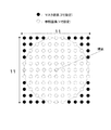
4は選択的加算部で、まず、11画素×11ラインデータを、図5に示した反射電子として影響を及ぼす周辺画素の情報を示すハレーションマスクパターンでマスクする(マスク領域の画素量は0となる。)。
次に、スペーサ近傍の注目画素において、周囲の画素からの反射電子のスペーサにより遮断された分のみを選択的に加算する。注目画素がスペーサ近傍にあるかどうかは、スペーサ位置情報生成部5が、タイミング制御部13より受け取ったタイミング制御信号とスペーサ位置情報を元に生成した注目画素とスペーサとの位置関係を示すSPD値(Spacer
Distance)により判断する。スペーサ近傍の注目画素における遮断された反射電子に対
応する画素は図6のようにSPD値により10パターンあり、遮断量に関係する総点灯量は、SPD値に応じて黒丸で示した画素値を選択し、これらをすべて加算することで求めることができる。スペーサの非近傍に対しては、反射電子のスペーサによる遮断は起きないため、加算結果は0とすればよい。
Next, in the target pixel near the spacer, only the amount blocked by the spacer of the reflected electrons from the surrounding pixels is selectively added. Whether the pixel of interest is in the vicinity of the spacer is determined by the SPD value indicating the positional relationship between the pixel of interest and the spacer generated by the spacer position
Judge by Distance). The pixels corresponding to the blocked backscattered electrons in the pixel of interest near the spacer have 10 patterns according to the SPD value as shown in FIG. 6, and the total lighting amount related to the blocking amount is a pixel value indicated by a black circle according to the SPD value. Select and add all of them. Since the backscattered electrons are not blocked by the spacer in the vicinity of the spacer, the addition result may be zero.
6は係数乗算部であり、加算結果のうち何%が遮断されたハレーション分(抑制量)になるかを示す係数(ハレーションゲイン値)を乗算する。係数は通常0と1の間の値を取り、実際のパネルにおいては1.5%程度の値である。係数乗算部6により算出した補正値は、第2のメモリ7に格納される。
第2のメモリ7の役割は、算出した補正値を、第1のメモリ2を経由していない元画像データの所定の画素位置に対応させるべくタイミング調整をすることであり、本構成では1フレーム遅延を行うため、補正値を格納するフレームバッファとなる。第2のメモリ7はタイミング調整バッファとして機能するので、外付けのDRAMなどの安価なデバイスを用いることが好ましい。
The role of the
1フレーム後に第2のメモリ7から読み出された補正値は、補正演算部8で元画像データに、
「Rout=Rin+補正値,
Gout=Gin+補正値,
Bout=Bin+補正値」
のように加算演算され補正データとして出力する。
The correction value read from the
“Rout = Rin + correction value,
Gout = Gin + correction value,
Bout = Bin + correction value ”
In this way, addition is performed and output as correction data.
以上説明したように、補正精度を落とさずにコスト低減が図れるように、補正を第1のメモリ2と第2のメモリ7のように分離した構成で行う方式を説明した。以上のような方法を用いることで、補正データを1フレーム遅延後に反映させることによる弊害が懸念されたが、実験では視認されず良好な補正結果を得ることができた。この理由は、通常の映像はフレーム間に強い相関性があり、1フレーム遅延での相違は検知できないケースが多いことと、仮に、フレーム相関性が弱い映像(黒背景に白の矩形領域が1フレーム単位で移動する映像など)が来た場合でもハレーションの補正量は前述した通りに輝点の輝度の1.5%程度と小さいため補正誤差としての輝度変化に関して人間の目の検知限界を超えているためであると考えられる。これにより、図8(a)のような補正前にはスペーサ近傍の色純度の段階的な変化は図8(b)に示したようにスペーサ近傍に遮断された反射電子分にハレーションが加算され、画面全体としてスペーサ非近傍と近傍の色純度の違いが低減し、ハレーションによるスペーサむらを補正することができる。
As described above, the method has been described in which the correction is performed in a separate configuration such as the
このように、本発明は、補正値を求める信号経路に元画像データを入れてしまうと、間引き処理を行うために元画像データも間引かれ、良好な画像を得ることができなくなるという問題を解決するためになされたものである。このため、本発明は、元画像データの信号経路と、補正値を求める信号経路とを分け、それに伴ってタイミングの遅延が発生するので第2のメモリによってタイミングをとり、元画像データと補正値との良好な補正演算
を可能とし、良好な画像を得ている。
As described above, according to the present invention, if the original image data is put in the signal path for obtaining the correction value, the original image data is also thinned for performing the thinning process, and a good image cannot be obtained. It was made to solve. Therefore, according to the present invention, the signal path for the original image data and the signal path for obtaining the correction value are separated, and a timing delay is generated accordingly. With this, it is possible to obtain a good image.
なお、本実施形態では、補正値を元画像データに加算する形態を説明した。しかし、これに限られず、補正値をゲインとして記憶しておいて補正値を元画像データに乗算する形態などの他の形態であってもよい。すなわち、全画素に同一の明るさを要求する画像データ(各画素に対応する入力画素データが同一の値を持つ)が入力された場合に、遮蔽部材近傍の明るさが遮蔽部材が存在することによって遮蔽部材の非近傍の明るさよりも小さくなる構成において、遮蔽部材近傍と遮蔽部材非近傍との明るさの差が少なくなるように、遮蔽部材近傍の画素に対応する画素データが遮蔽部材非近傍の画素に対応する画素データに対して相対的に大きくなる補正ができる形態であれば種々の形態を採用することができる。 In the present embodiment, the mode in which the correction value is added to the original image data has been described. However, the present invention is not limited to this, and other forms such as a form in which the correction value is stored as a gain and the correction value is multiplied by the original image data may be used. That is, when image data that requires the same brightness for all pixels (input pixel data corresponding to each pixel has the same value) is input, the brightness of the vicinity of the shielding member is present in the shielding member. The pixel data corresponding to the pixels in the vicinity of the shielding member is not in the vicinity of the shielding member so that the difference in brightness between the vicinity of the shielding member and the vicinity of the shielding member is reduced. Various forms can be adopted as long as the correction is relatively large with respect to the pixel data corresponding to the pixels.
(第2の実施形態)
第1の実施形態では、スペーサ近傍領域においてスペーサにより遮断された反射電子を推定し遮断分のハレーション分(抑制量)を加算することでスペーサむらを補正する例について説明した。本実施形態では、図9(a)に示したように、スペーサ非近傍とスペーサ近傍それぞれにある元々あるハレーション分(影響量)を推定し元画像データから減算することでスペーサむらを含むむらを図9(b)に示したように補正する。本実施形態は、第1の実施形態の構成が同様に適用できることから第1の実施形態との相違点のみ示した形で説明する。
(Second Embodiment)
In the first embodiment, an example has been described in which the backscattered electrons blocked by the spacers in the region near the spacers are estimated, and the unevenness of the spacers is corrected by adding the blocked halation amount (suppression amount). In this embodiment, as shown in FIG. 9A, the original halation amount (influence amount) in each of the non-spacer vicinity and the vicinity of the spacer is estimated and subtracted from the original image data to remove the unevenness including the spacer unevenness. Correction is performed as shown in FIG. In the present embodiment, since the configuration of the first embodiment can be similarly applied, only the differences from the first embodiment will be described.
第1の実施形態との違いは、選択的加算部4の内部処理で、図7のようにSPD値により11パターンあり、SPD値(スペーサの非近傍はSPD=0、スペーサの近傍はSP
D=1〜10)により黒丸で示した画素値を選択し、すべて加算することで、元々あるハ
レーション分を推定する点である。このようにフィルタパターンを構成することによって、スペーサによって影響が遮断されない周辺画素の画素データ(間引きされている)を積算することが可能となっている。また、本実施形態では周辺画素が駆動されることによる所定画素の明るさの増分を補正する構成となっている。このため、1フレーム後に第2のメモリ7から読み出された補正値は、補正演算部8で元画像データに、
「Rout=Rin−補正値,
Gout=Gin−補正値,
Bout=Bin−補正値」
のように減算演算した補正データとして出力する。これ以外は第1の実施形態と同様である。
The difference from the first embodiment is the internal processing of the
The pixel values indicated by black circles are selected according to D = 1 to 10) and all are added to estimate the original halation. By configuring the filter pattern in this way, it is possible to integrate the pixel data (thinned out) of peripheral pixels whose influence is not blocked by the spacer. In the present embodiment, the increase in brightness of a predetermined pixel due to driving of peripheral pixels is corrected. Therefore, the correction value read from the
“Rout = Rin−correction value,
Gout = Gin−correction value,
Bout = Bin−correction value ”
Is output as correction data obtained by the subtraction operation. The rest is the same as in the first embodiment.
したがって、本実施形態においても、図1の補正を第1のメモリと第2のメモリのように分離した構成を第1の実施形態と同様に適用することが可能で、それにより補正精度を落とさずにコスト低減が図れるという第1の実施形態と同様な効果を得ることができる。本実施形態ではスペーサ非近傍におけるハレーションの影響によるむらを補正できる。従って、本実施形態は表示領域において画素間の相互の影響を局所的に異ならしめる遮蔽部材が存在しない構成においても適用可能なものである。本実施形態では、遮蔽部材非近傍のむらを補正すると共に、該補正の程度を遮蔽部材近傍においては調整できるようにすることで遮蔽部材近傍でも適切なむら補正ができるようになっている。ただし、周辺画素の駆動によって表示階調が大きくなる影響を減らすための補正を行うので、元画像データが補正値よりも小さい場合には該補正は制限を受けることになる。元画像データが補正値よりも大きい場合には遮蔽部材非近傍を含めて完全な補正を行うことが可能である。 Therefore, also in the present embodiment, the configuration in which the correction of FIG. 1 is separated as in the first memory and the second memory can be applied in the same manner as in the first embodiment, thereby reducing the correction accuracy. It is possible to obtain the same effect as that of the first embodiment in which cost reduction can be achieved. In this embodiment, unevenness due to halation in the vicinity of the spacer can be corrected. Therefore, the present embodiment can also be applied to a configuration in which there is no shielding member that locally varies the mutual influence between pixels in the display area. In the present embodiment, unevenness in the vicinity of the shielding member is corrected, and the degree of correction can be adjusted in the vicinity of the shielding member, so that appropriate unevenness correction can be performed in the vicinity of the shielding member. However, since correction is performed to reduce the effect of increasing the display gradation by driving peripheral pixels, the correction is limited when the original image data is smaller than the correction value. When the original image data is larger than the correction value, it is possible to perform complete correction including the vicinity of the shielding member.
(第3の実施形態)
第1、第2の実施形態では、間引き処理部1で元画像データを減じる方法について説明したが、いずれの場合も元画像データ11画素×11ラインの全画素を参照する方式であ
った。本実施形態では更なるメモリ容量の削減を行うために、ライン間引き法について図10を用いて説明する。
(Third embodiment)
In the first and second embodiments, the method of reducing the original image data by the thinning
間引き制御部1において、第1の実施形態で説明した方法で元データを減じた後、ライン間引きを行う。具体的には、図10(a)に示したように、奇数ライン(l+1,l+3,l+5,l+7,l+9)のデータのみ第1のメモリ2に飛び越しで書き込む制御を行う。
In the thinning
従って、第1のメモリ2には5ライン分の奇数ラインデータが格納される。次に5ライン分のデータが格納された時点で演算参照のために5ラインメモリから同時に11画素×5ラインのデータが読み出されていく。補間部3では第1の実施形態で減じた分を同様に2n−m倍にすることに加えて、ライン間引きされた偶数ライン(l,l+2,l+4,l+6,l+8,l+10)のデータを推定により補間再生させる処理を行う。
Therefore, odd line data for 5 lines is stored in the
このライン補間方法の一例としては補間すべき画素の上下ラインのオリジナル画素から線形補間で求める方法がある。例えば、(p+2,l+2)の位置にある補間画素値D(p+2,l+2)を求める場合は、D(p+2,l+2)=(D(p+2,l+1)+D(p+2,l+3))/2のように簡易な計算で算出できる。このようなライン補間の方法は、上記の線形補間法に限定するものではなく、補間画素の周囲4×4の範囲を参照したキュービック補間法や最近傍補間法など他の一般的な手法を適用しても良い。 As an example of this line interpolation method, there is a method of obtaining by linear interpolation from original pixels on the upper and lower lines of the pixel to be interpolated. For example, when the interpolated pixel value D (p + 2, l + 2) at the position (p + 2, l + 2) is obtained, D (p + 2, l + 2) = (D (p + 2, l + 1) + D (p + 2, l + 3)) / 2 It can be calculated with simple calculation. Such a line interpolation method is not limited to the linear interpolation method described above, and other general methods such as a cubic interpolation method or a nearest neighbor interpolation method referring to a 4 × 4 range around the interpolation pixel are applied. You may do it.
補間部3の出力は11画素×11ライン分のデータとして選択的加算部4に入力する。それ以後の処理は第1の実施形態と同様になる。
The output of the
また、上記説明のフレーム期間は、奇数ラインのデータを取り込み、偶数ラインを補間したが、次のフレームは、図10(b)に示したように、偶数ラインのデータを取り込み奇数ラインを補間し、以降、フレームごとに間引きパターンを奇数と偶数をトグルするような処理を行うことが好ましい。この理由は補間するラインが常に同じであるよりも参照画素を平準化した方が補間による補正性能が低下しずらくなると考えられるためである。 In the frame period described above, odd line data is captured and even lines are interpolated. In the next frame, even line data is captured and odd lines are interpolated as shown in FIG. 10B. Henceforth, it is preferable to perform a process of toggling between an odd number and an even number as a thinning pattern for each frame. This is because it is considered that correction performance by interpolation is less likely to be reduced when the reference pixels are leveled than when the lines to be interpolated are always the same.
以上のように、ライン間引きで元画像データを減じる方法を行うことで、ラインメモリ容量は第1の実施形態より更に約50%まで削減することが可能になる。 As described above, by performing the method of reducing the original image data by line thinning, the line memory capacity can be further reduced to about 50% compared to the first embodiment.
なお、上記実施形態は、ライン方向の間引きの例を上げたが、画素方向に間引き方法を適用しても良い。また、ライン方向、画素方向ともに間引けば25%まで削減することが可能であることは明らかである。 In the above-described embodiment, an example of thinning in the line direction is given, but a thinning method may be applied in the pixel direction. In addition, it is clear that if the line direction and the pixel direction are thinned out, it can be reduced to 25%.
そして、本実施形態も、図1に示した第1のメモリ1と第2のメモリ7のように分離した構成をとることで実現可能になるものであり、第1、第2の実施形態よりも更なるコスト低減効果を得ることができる。
This embodiment can also be realized by adopting a separate configuration such as the
1 間引き処理部
2 第1のメモリ
3 補間部
4 選択的加算部
5 スペーサ位置情報生成部
6 係数乗算部
7 第2のメモリ
10 信号処理部
11 逆γ補正部
12 ハレーション補正部
13 タイミング制御部
20 表示パネル
DESCRIPTION OF
Claims (10)
所定画面の所定画素の近傍に位置する複数の周辺画素に対応する画素信号として順次入力される複数の画素信号に対して間引き処理を行った信号を記憶する第1メモリと、
補正値を前記第1メモリからの出力に基づいて算出する算出回路と、
前記所定画面よりも後の画面において前記所定画素を形成するための画素信号であって前記第1メモリを経由していない画素信号を、前記所定画面に対応する前記補正値で補正できるように前記補正値を出力するタイミングを調整するための第2メモリと、
前記所定画面よりも後の画面において前記所定画素を形成するための前記画素信号であって前記第1メモリを経由していない前記画素信号を、前記所定画面に対応する前記補正値で補正する演算を行う演算回路と、
を有しており、
前記補正値は、前記複数の周辺画素による前記所定画素の表示階調への影響が、補正された画素信号に基づいて画像表示する表示パネルが有する遮蔽部材によって抑制された量に対応する補正を行うための補正値である補正回路。 A correction circuit for correcting a pixel signal,
A first memory for storing a signal obtained by performing a thinning process on a plurality of pixel signals sequentially input as pixel signals corresponding to a plurality of peripheral pixels located in the vicinity of a predetermined pixel on a predetermined screen;
A calculation circuit that calculates a correction value based on an output from the first memory;
The pixel signal for forming the predetermined pixel in a screen after the predetermined screen and not passing through the first memory can be corrected with the correction value corresponding to the predetermined screen. A second memory for adjusting the timing of outputting the correction value;
Computation for correcting the pixel signal for forming the predetermined pixel on the screen after the predetermined screen but not passing through the first memory with the correction value corresponding to the predetermined screen. An arithmetic circuit for performing
Have
The correction value is a correction corresponding to an amount in which the influence of the plurality of peripheral pixels on the display gradation of the predetermined pixel is suppressed by a shielding member included in a display panel that displays an image based on the corrected pixel signal. A correction circuit which is a correction value for performing.
前記算出回路は、第1メモリからの出力後に間引いた画素を周辺画素から補間して生成し、前記算出を行う請求項1に記載の補正回路。 The thinning process is a thinning process in which a plurality of pixels arranged in a horizontal direction and / or a vertical direction are thinned out for each column.
The correction circuit according to claim 1, wherein the calculation circuit performs the calculation by interpolating and generating pixels thinned out after output from the first memory from surrounding pixels.
前記画素信号であって前記第1メモリを経由していない前記画素信号に、前記補正値を加算演算する請求項1に記載の補正回路。 The arithmetic circuit adds and calculates the correction value to the pixel signal for forming the predetermined pixel in a screen after the predetermined screen and not passing through the first memory. Item 2. The correction circuit according to Item 1.
所定画面の所定画素の近傍に位置する複数の周辺画素に対応する画素信号として順次入力される複数の画素信号に対して間引き処理を行った信号を記憶する第1メモリと、
前記複数の周辺画素による前記所定画素の表示階調への影響を補正するための補正値を前記第1メモリからの出力に基づいて算出する算出回路と、
前記所定画面よりも後の画面において前記所定画素を形成するための画素信号であって前記第1メモリを経由していない画素信号を、前記所定画面に対応する前記補正値で補正できるように前記補正値を出力するタイミングを調整するための第2メモリと、
前記所定画面よりも後の画面において前記所定画素を形成するための前記画素信号であって前記第1メモリを経由していない前記画素信号を、前記所定画面に対応する前記補正値で補正する演算を行う演算回路と、
を有する補正回路。 A correction circuit for correcting a pixel signal,
A first memory for storing a signal obtained by performing a thinning process on a plurality of pixel signals sequentially input as pixel signals corresponding to a plurality of peripheral pixels located in the vicinity of a predetermined pixel on a predetermined screen;
A calculation circuit that calculates a correction value for correcting the influence of the plurality of peripheral pixels on the display gradation of the predetermined pixel based on an output from the first memory;
The pixel signal for forming the predetermined pixel on the screen after the predetermined screen and not passing through the first memory can be corrected with the correction value corresponding to the predetermined screen. A second memory for adjusting the timing of outputting the correction value;
Computation for correcting the pixel signal for forming the predetermined pixel on a screen after the predetermined screen but not passing through the first memory with the correction value corresponding to the predetermined screen An arithmetic circuit for performing
A correction circuit.
前記補正回路で補正された画素信号によって画像表示する表示パネルと、
を備える画像表示装置。 A correction circuit according to any one of claims 1 to 7,
A display panel for displaying an image by the pixel signal corrected by the correction circuit;
An image display device comprising:
発光体と、A light emitter;
スペーサと、A spacer;
電子放出素子を駆動するための画素信号を補正する補正回路と、を有しており、前記電子放出素子から放出される電子が前記発光体に照射されることによる発光で画素を形成する画像表示装置であって、And a correction circuit that corrects a pixel signal for driving the electron-emitting device, and forms an image by forming light emission by irradiating the light-emitting body with electrons emitted from the electron-emitting device. A device,
前記補正回路は、The correction circuit includes:
所定画面の所定画素に対して、前記スペーサとは反対の側の画素に対応する画素信号に対して間引き処理を行った信号を記憶する第1メモリと、A first memory for storing a signal obtained by performing a thinning process on a pixel signal corresponding to a pixel on the opposite side of the spacer with respect to a predetermined pixel of a predetermined screen;
補正値を前記第1メモリからの出力に基づいて算出する算出回路と、A calculation circuit that calculates a correction value based on an output from the first memory;
前記所定画面よりも後の画面において前記所定画素を形成するための画素信号であって前記第1メモリを経由していない画素信号を、前記所定画面に対応する前記補正値で補正できるように前記補正値を出力するタイミングを調整するための第2メモリと、The pixel signal for forming the predetermined pixel on the screen after the predetermined screen and not passing through the first memory can be corrected with the correction value corresponding to the predetermined screen. A second memory for adjusting the timing of outputting the correction value;
前記所定画面よりも後の画面において前記所定画素を形成するための前記画素信号であって前記第1メモリを経由していない前記画素信号を、前記所定画面に対応する前記補正値で補正する演算を行う演算回路と、Computation for correcting the pixel signal for forming the predetermined pixel on a screen after the predetermined screen but not passing through the first memory with the correction value corresponding to the predetermined screen An arithmetic circuit for performing
を有していることを特徴とする画像表示装置。An image display device comprising:
該チューナーで受信した信号に基づく画像表示を行う請求項8もしくは9に記載の画像表示装置と、
を備えるテレビジョン装置。 A tuner for receiving a television signal;
The image display device according to claim 8 or 9, which performs image display based on a signal received by the tuner;
A television apparatus comprising:
Priority Applications (2)
| Application Number | Priority Date | Filing Date | Title |
|---|---|---|---|
| JP2005165552A JP3870214B2 (en) | 2004-06-29 | 2005-06-06 | Correction circuit |
| US11/156,656 US7327506B2 (en) | 2004-06-29 | 2005-06-21 | Correction circuit |
Applications Claiming Priority (2)
| Application Number | Priority Date | Filing Date | Title |
|---|---|---|---|
| JP2004191824 | 2004-06-29 | ||
| JP2005165552A JP3870214B2 (en) | 2004-06-29 | 2005-06-06 | Correction circuit |
Publications (3)
| Publication Number | Publication Date |
|---|---|
| JP2006047987A JP2006047987A (en) | 2006-02-16 |
| JP2006047987A5 JP2006047987A5 (en) | 2006-08-03 |
| JP3870214B2 true JP3870214B2 (en) | 2007-01-17 |
Family
ID=35505316
Family Applications (1)
| Application Number | Title | Priority Date | Filing Date |
|---|---|---|---|
| JP2005165552A Expired - Fee Related JP3870214B2 (en) | 2004-06-29 | 2005-06-06 | Correction circuit |
Country Status (2)
| Country | Link |
|---|---|
| US (1) | US7327506B2 (en) |
| JP (1) | JP3870214B2 (en) |
Cited By (2)
| Publication number | Priority date | Publication date | Assignee | Title |
|---|---|---|---|---|
| US7817115B2 (en) | 2004-12-15 | 2010-10-19 | Canon Kabushiki Kaisha | Image display apparatus |
| US7830339B2 (en) | 2004-12-17 | 2010-11-09 | Canon Kabushiki Kaisha | Image display apparatus |
Families Citing this family (11)
| Publication number | Priority date | Publication date | Assignee | Title |
|---|---|---|---|---|
| JP4352025B2 (en) * | 2004-06-29 | 2009-10-28 | キヤノン株式会社 | Image display device |
| US20060092329A1 (en) * | 2004-10-29 | 2006-05-04 | Canon Kabushiki Kaisha | Image display apparatus and correction apparatus thereof |
| JP3870210B2 (en) * | 2004-12-17 | 2007-01-17 | キヤノン株式会社 | Image display apparatus and television apparatus |
| US8558765B2 (en) * | 2005-11-07 | 2013-10-15 | Global Oled Technology Llc | Method and apparatus for uniformity and brightness correction in an electroluminescent display |
| JP2007142500A (en) * | 2005-11-14 | 2007-06-07 | Pioneer Electronic Corp | Display device, signal processing circuit, program, and display method |
| JP2007199684A (en) * | 2005-12-28 | 2007-08-09 | Canon Inc | Image display apparatus |
| JP2007199683A (en) * | 2005-12-28 | 2007-08-09 | Canon Inc | Image display apparatus |
| JP2007271940A (en) * | 2006-03-31 | 2007-10-18 | Toshiba Corp | Video displaying device and video displaying method |
| JP2009150926A (en) | 2007-12-18 | 2009-07-09 | Canon Inc | Image display apparatus and manufacturing method thereof |
| US8554011B2 (en) * | 2011-06-07 | 2013-10-08 | Microsoft Corporation | Automatic exposure correction of images |
| US8928735B2 (en) * | 2011-06-14 | 2015-01-06 | Microsoft Corporation | Combined lighting, projection, and image capture without video feedback |
Family Cites Families (22)
| Publication number | Priority date | Publication date | Assignee | Title |
|---|---|---|---|---|
| JP3311201B2 (en) * | 1994-06-08 | 2002-08-05 | キヤノン株式会社 | Image forming device |
| JPH1124629A (en) | 1997-07-04 | 1999-01-29 | Mitsubishi Electric Corp | Display device for plasma display panel |
| JP3025251B2 (en) * | 1997-12-27 | 2000-03-27 | キヤノン株式会社 | Image display device and driving method of image display device |
| JP3592070B2 (en) | 1998-02-26 | 2004-11-24 | キヤノン株式会社 | Image forming device |
| JPH11250840A (en) | 1998-02-27 | 1999-09-17 | Canon Inc | Image forming device |
| JP2000056730A (en) * | 1998-06-05 | 2000-02-25 | Canon Inc | Device and method to form image |
| JP3592126B2 (en) | 1999-02-26 | 2004-11-24 | キヤノン株式会社 | Image display device and control method thereof |
| JP2001013482A (en) | 1999-04-28 | 2001-01-19 | Sharp Corp | Matrix display device and plasma address display device |
| US6307327B1 (en) * | 2000-01-26 | 2001-10-23 | Motorola, Inc. | Method for controlling spacer visibility |
| US6842160B2 (en) * | 2000-11-21 | 2005-01-11 | Canon Kabushiki Kaisha | Display apparatus and display method for minimizing decreases in luminance |
| JP3937906B2 (en) | 2001-05-07 | 2007-06-27 | キヤノン株式会社 | Image display device |
| JP2002335444A (en) | 2001-05-08 | 2002-11-22 | Canon Inc | Multi-screen display device, multi-screen display method, recording medium, and program |
| US6712660B2 (en) * | 2001-08-06 | 2004-03-30 | Canon Kabushiki Kaisha | Method and apparatus for adjusting characteristics of electron source, and method for manufacturing electron source |
| JP5022547B2 (en) * | 2001-09-28 | 2012-09-12 | キヤノン株式会社 | Image forming apparatus characteristic adjusting method, image forming apparatus manufacturing method, image forming apparatus, and characteristic adjusting apparatus |
| US6952193B2 (en) * | 2001-12-12 | 2005-10-04 | Canon Kabushiki Kaisha | Image display apparatus and image display methods |
| JP3962728B2 (en) * | 2003-06-20 | 2007-08-22 | キヤノン株式会社 | Image display device |
| US7953819B2 (en) * | 2003-08-22 | 2011-05-31 | Emc Corporation | Multi-protocol sharable virtual storage objects |
| JP4047316B2 (en) * | 2003-09-25 | 2008-02-13 | キヤノン株式会社 | Frame rate conversion device, overtaking prediction method used therefor, display control device, and video reception display device |
| US7825987B2 (en) * | 2003-10-03 | 2010-11-02 | Canon Kabushiki Kaisha | Information processor, TV system, control method and program |
| JP4366182B2 (en) * | 2003-12-09 | 2009-11-18 | キヤノン株式会社 | Broadcast receiving apparatus and method for controlling broadcast receiving apparatus |
| JP4352025B2 (en) * | 2004-06-29 | 2009-10-28 | キヤノン株式会社 | Image display device |
| JP3870210B2 (en) * | 2004-12-17 | 2007-01-17 | キヤノン株式会社 | Image display apparatus and television apparatus |
-
2005
- 2005-06-06 JP JP2005165552A patent/JP3870214B2/en not_active Expired - Fee Related
- 2005-06-21 US US11/156,656 patent/US7327506B2/en not_active Expired - Fee Related
Cited By (2)
| Publication number | Priority date | Publication date | Assignee | Title |
|---|---|---|---|---|
| US7817115B2 (en) | 2004-12-15 | 2010-10-19 | Canon Kabushiki Kaisha | Image display apparatus |
| US7830339B2 (en) | 2004-12-17 | 2010-11-09 | Canon Kabushiki Kaisha | Image display apparatus |
Also Published As
| Publication number | Publication date |
|---|---|
| US20050286062A1 (en) | 2005-12-29 |
| JP2006047987A (en) | 2006-02-16 |
| US7327506B2 (en) | 2008-02-05 |
Similar Documents
| Publication | Publication Date | Title |
|---|---|---|
| US7298094B2 (en) | Image display apparatus | |
| US7046219B2 (en) | Image display apparatus having a circuit for correcting a driving signal that drives electron emitting devices | |
| JP4770619B2 (en) | Display image correction apparatus, image display apparatus, and display image correction method | |
| JP3870214B2 (en) | Correction circuit | |
| US8068070B2 (en) | Image display apparatus | |
| JP2007199683A (en) | Image display apparatus | |
| US20090309814A1 (en) | Image display apparatus and television apparatus | |
| US20100013870A1 (en) | Image display apparatus and correction method of image signal | |
| JP4154422B2 (en) | Image display device | |
| JP4154423B2 (en) | Image display device | |
| US20060012613A1 (en) | Image processing device and image processing method | |
| JP2009150926A (en) | Image display apparatus and manufacturing method thereof | |
| JP2004240186A (en) | Flat panel display device, driving circuit for display, and driving method for display | |
| KR20060028919A (en) | Method of correcting gray-scale data for driving electron emission display panel | |
| WO2012141114A1 (en) | Image display device and image display method | |
| JP4137149B2 (en) | Image display device | |
| JP2006106143A (en) | Device and method for display | |
| JP2006023578A (en) | Flat panel display device and luminance control method for display device | |
| JP2006106145A (en) | Display device |
Legal Events
| Date | Code | Title | Description |
|---|---|---|---|
| A521 | Request for written amendment filed |
Free format text: JAPANESE INTERMEDIATE CODE: A523 Effective date: 20060620 |
|
| A621 | Written request for application examination |
Free format text: JAPANESE INTERMEDIATE CODE: A621 Effective date: 20060620 |
|
| A871 | Explanation of circumstances concerning accelerated examination |
Free format text: JAPANESE INTERMEDIATE CODE: A871 Effective date: 20060620 |
|
| A975 | Report on accelerated examination |
Free format text: JAPANESE INTERMEDIATE CODE: A971005 Effective date: 20060707 |
|
| A977 | Report on retrieval |
Free format text: JAPANESE INTERMEDIATE CODE: A971007 Effective date: 20060926 |
|
| TRDD | Decision of grant or rejection written | ||
| A01 | Written decision to grant a patent or to grant a registration (utility model) |
Free format text: JAPANESE INTERMEDIATE CODE: A01 Effective date: 20061003 |
|
| A61 | First payment of annual fees (during grant procedure) |
Free format text: JAPANESE INTERMEDIATE CODE: A61 Effective date: 20061016 |
|
| R150 | Certificate of patent or registration of utility model |
Free format text: JAPANESE INTERMEDIATE CODE: R150 |
|
| FPAY | Renewal fee payment (event date is renewal date of database) |
Free format text: PAYMENT UNTIL: 20091020 Year of fee payment: 3 |
|
| FPAY | Renewal fee payment (event date is renewal date of database) |
Free format text: PAYMENT UNTIL: 20101020 Year of fee payment: 4 |
|
| FPAY | Renewal fee payment (event date is renewal date of database) |
Free format text: PAYMENT UNTIL: 20101020 Year of fee payment: 4 |
|
| FPAY | Renewal fee payment (event date is renewal date of database) |
Free format text: PAYMENT UNTIL: 20111020 Year of fee payment: 5 |
|
| FPAY | Renewal fee payment (event date is renewal date of database) |
Free format text: PAYMENT UNTIL: 20111020 Year of fee payment: 5 |
|
| FPAY | Renewal fee payment (event date is renewal date of database) |
Free format text: PAYMENT UNTIL: 20121020 Year of fee payment: 6 |
|
| FPAY | Renewal fee payment (event date is renewal date of database) |
Free format text: PAYMENT UNTIL: 20131020 Year of fee payment: 7 |
|
| LAPS | Cancellation because of no payment of annual fees |