JP3868293B2 - Semiconductor integrated circuit - Google Patents
Semiconductor integrated circuit Download PDFInfo
- Publication number
- JP3868293B2 JP3868293B2 JP2001400655A JP2001400655A JP3868293B2 JP 3868293 B2 JP3868293 B2 JP 3868293B2 JP 2001400655 A JP2001400655 A JP 2001400655A JP 2001400655 A JP2001400655 A JP 2001400655A JP 3868293 B2 JP3868293 B2 JP 3868293B2
- Authority
- JP
- Japan
- Prior art keywords
- node
- semiconductor integrated
- logic level
- transistor
- integrated circuit
- Prior art date
- Legal status (The legal status is an assumption and is not a legal conclusion. Google has not performed a legal analysis and makes no representation as to the accuracy of the status listed.)
- Expired - Fee Related
Links
- 239000004065 semiconductor Substances 0.000 title claims description 152
- 230000007423 decrease Effects 0.000 claims description 7
- 238000010586 diagram Methods 0.000 description 24
- 238000011156 evaluation Methods 0.000 description 20
- 230000003068 static effect Effects 0.000 description 12
- 101001124039 Banna virus (strain Indonesia/JKT-6423/1980) Non-structural protein 4 Proteins 0.000 description 3
- 101000933041 His1 virus (isolate Australia/Victoria) Major capsid protein Proteins 0.000 description 3
- 101710192266 Tegument protein VP22 Proteins 0.000 description 3
- 230000007257 malfunction Effects 0.000 description 3
- 238000000034 method Methods 0.000 description 2
- 241001581521 Attila spadiceus Species 0.000 description 1
- 230000000694 effects Effects 0.000 description 1
- 230000005669 field effect Effects 0.000 description 1
- XDDAORKBJWWYJS-UHFFFAOYSA-N glyphosate Chemical compound OC(=O)CNCP(O)(O)=O XDDAORKBJWWYJS-UHFFFAOYSA-N 0.000 description 1
- 229910044991 metal oxide Inorganic materials 0.000 description 1
- 150000004706 metal oxides Chemical class 0.000 description 1
Images
Classifications
-
- H—ELECTRICITY
- H03—ELECTRONIC CIRCUITRY
- H03K—PULSE TECHNIQUE
- H03K19/00—Logic circuits, i.e. having at least two inputs acting on one output; Inverting circuits
- H03K19/02—Logic circuits, i.e. having at least two inputs acting on one output; Inverting circuits using specified components
- H03K19/08—Logic circuits, i.e. having at least two inputs acting on one output; Inverting circuits using specified components using semiconductor devices
- H03K19/094—Logic circuits, i.e. having at least two inputs acting on one output; Inverting circuits using specified components using semiconductor devices using field-effect transistors
- H03K19/096—Synchronous circuits, i.e. using clock signals
- H03K19/0963—Synchronous circuits, i.e. using clock signals using transistors of complementary type
Description
【0001】
【発明の属する技術分野】
本発明は、半導体集積回路に関し、特に、論理回路に関する。
【0002】
【従来の技術】
近年の半導体集積回路においては、プロセスを微細化して、動作の高速化、省面積化、低消費電力化等が実現されてきている。プロセスを微細化し、トランジスタのゲート長が短くなると、トランジスタがオンの状態のときに流れるトランジスタの単位ゲート幅当たりのドレイン電流量が増加するというメリットがある。一方、トランジスタがオフの状態のときに流れるドレイン−ソース間のリーク電流(以下では、サブスレッショルド電流と称する)が増加してしまうという問題がある。微細化に伴うこのサブスレッショルド電流の増加率は、トランジスタがオンの状態のときに流れるドレイン電流量の増加率よりも大きい。
【0003】
図11は、従来のダイナミック型の半導体集積回路の例を示す回路図である。図11の回路は、PMOSトランジスタ2101,2102と、入力回路2120と、出力回路2130とを備えている。入力回路2120は、NMOSトランジスタ2121,2122を備え、出力回路2130は、PMOSトランジスタ2131と、NMOSトランジスタ2132とを備えている。図11の回路は、入力信号VI1及びVI2の論理和を求めて出力する回路である。
【0004】
クロック信号CLKが“L”(低論理レベル)の期間はプリチャージ期間である。この期間において、PMOSトランジスタ2101がオンになって、ノードN211をプリチャージする。入力信号VI1,VI2は、“L”の状態を続ける。
【0005】
クロック信号CLKが“H”(高論理レベル)の期間は評価期間である。この期間において、入力信号VI1及びVI2はアクティブになる。入力信号VI1及びVI2のうちのいずれかが“H”になると、ノードN211はディスチャージされ、出力信号V21は“H”になる。入力信号VI1及びVI2がともに“L”であれば、ノードN211はディスチャージされず、出力信号V21は“L”である。このとき、PMOSトランジスタ2101がオンであって、ノードN211の電位を“H”に保持する。
【0006】
図12は、従来のスタティック型の半導体集積回路の例を示す回路図である。図12の回路は、インバータが2段直列に接続されたバッファ回路として動作する。図12の回路は、PMOSトランジスタ2231と、NMOSトランジスタ2232とを有するインバータと、PMOSトランジスタ2281と、NMOSトランジスタ2282とを有するインバータとを備えている。
【0007】
【発明が解決しようとする課題】
図14のような構成のダイナミック回路において、トランジスタがオフのときに流れるサブスレッショルド電流が、トランジスタがオンのときに流れるドレイン電流に比べて無視できないようになった場合について説明する。
【0008】
評価期間において、入力信号VI1,VI2がともに“L”であるとしても、NMOSトランジスタ2121,2122にはサブスレッショルド電流が流れる。このとき、電源からPMOSトランジスタ2102と、NMOSトランジスタ2121又は2122とを通って、接地線に電流が流れる。このとき、ノードN211の電位は、電源電位VDDよりも電圧Vdだけ低い値となる。
【0009】
ここで、電圧VdがPMOSトランジスタ2131のスレッショルド電圧Vt(トランジスタがオフの状態からオンの状態に切り替わる時の、そのゲート−ソース間の電圧)よりも小さければ、PMOSトランジスタ2131はオフ、NMOSトランジスタ2132がオンとなり、出力信号V21は“L”になる。このときの出力信号V21の電位は、接地電位VSSよりも高い値となる。PMOSトランジスタ2131の抵抗値をR2131、NMOSトランジスタ2132の抵抗値をr2132すると、出力信号V21の電位の接地電位VSSからのシフトVdoは、VDD*r2132/(R2131+r2132)となる。
【0010】
また、電圧VdがPMOSトランジスタ2131のスレッショルド電圧Vtよりも大きければ、このトランジスタがオンになってしまう。PMOSトランジスタ2131と、NMOSトランジスタ2132とがともにオンになるので、出力が不定になる他、これらのトランジスタに大きな貫通電流が流れてしまう。
【0011】
プリチャージ期間においても、NMOSトランジスタ2121,2122にサブスレッショルド電流が流れると、ノードN211の電位は電源電位VDDよりも小さくなるので、同様のことが生じ得る。
【0012】
サブスレッショルド電流は、トランジスタのゲート−ソース間の電圧Vgsに対して指数関数的に増加するという性質があるので、PMOSトランジスタ2131のゲート−ソース間電圧Vgsが電圧Vdである場合には、このトランジスタにはVgs=0のときに比べて大きな電流が流れることになり、出力信号V21の電位のシフトVdoが大きな値となってしまう。
【0013】
このように、サブスレッショルド電流を無視できない場合には、出力信号V21の電位のシフト、すなわち、出力されるDCノイズが無視できない程大きなものとなる。特に、入力信号に含まれていたDCノイズよりも出力信号に含まれるDCノイズの方が大きい場合には、DCノイズが増幅されたことになる。
【0014】
このような現象については、文献Atila Alvandpour et. al. 2001 Symposium on VLSI Circuits Digest of Technical Papers 3-4, "A conditional Keeper Technique for Sub-0.13μ Wide Dynamic Gates"に記述されている。
【0015】
入力信号に含まれるDCノイズを増幅して出力してしまうような回路を複数直列に接続すると、DCノイズがだんだん大きくなって、ついには回路が誤動作してしまう。また、回路がDCノイズを増幅しないような場合であっても、電圧Vdや出力信号V21の電位のシフトVdoが大きな値となると、電源と接地線との間に流れるリーク電流が指数関数的に大きくなるので、トランジスタがオフであるときの消費電力が大きくなってしまうという問題点があった。
【0016】
図15のような構成のスタティック回路においても、トランジスタがオフのときに流れるサブスレッショルド電流が、トランジスタがオンのときに流れるドレイン電流に比べて無視できないようになった場合には、同様の問題がある。
【0017】
すなわち、PMOSトランジスタ2231にサブスレッショルド電流が流れるので、入力信号VIが“H”であっても、ノードN221の電位は接地電位VSSよりも高くなる。このため、出力信号V22の電位は電源電位VDDよりも低い値となる。すなわち、出力信号V22にはDCノイズが含まれる。入力信号に含まれていたDCノイズよりも出力信号に含まれるDCノイズの方が大きい場合には、DCノイズが増幅されたことになる。やはり、入力信号に含まれるDCノイズを増幅して出力してしまうような回路を複数直列に接続すると、回路が誤動作してしまう。
【0018】
本発明は、DCノイズの少ない信号を出力する半導体集積回路を提供することを課題とする。
【0019】
【課題を解決するための手段】
前記課題を解決するため、請求項1の発明が講じた手段は、半導体集積回路として、クロック信号に応じて第1のノードを第1の論理レベルにする第1のトランジスタと、入力信号に応じて前記第1のノードを前記第1の論理レベルとは異なる第2の論理レベルにする入力回路と、前記第1のノードが前記第1の論理レベルとなるときに第2のノードを前記第1の論理レベルになるようにする第2のトランジスタと、前記第1のノードと前記第2のノードとの間に接続され、前記第1のノードが前記第1の論理レベルであるときに抵抗値が大きくなり、前記第2の論理レベルであるときに抵抗値が小さくなる第1の抵抗素子と、前記第2のノードを入力とし、出力ノードを前記第1の論理レベルにするか否かを制御する第1の駆動トランジスタと、前記第1のノードと同一の論理レベルの信号を入力とし、前記出力ノードを前記第2の論理レベルにするか否かを制御する第2の駆動トランジスタとを備えるものである。
【0020】
請求項1の発明によると、第1の抵抗素子を備えているので、第1の駆動トランジスタがオフとなるときに、このトランジスタのゲート−ソース間電圧の絶対値を小さくすることができる。このため、クロックに同期して動作するダイナミック回路において、第1の駆動トランジスタのサブスレッショルド電流を削減することができるので、出力信号に含まれるDCノイズを小さくすることができる。
【0021】
また、請求項2の発明では、請求項1に記載の半導体集積回路において、前記第2のトランジスタは、前記クロック信号に応じて前記第2のノードを前記第1の論理レベルにするものである。
【0022】
また、請求項3の発明は、請求項1に記載の半導体集積回路において、前記第1のノードの論理レベルを反転して出力するインバータを更に備え、前記第2のトランジスタは、前記インバータの出力信号を入力とし、前記第1のノードが前記第1の論理レベルであるときに前記第2のノードを前記第1の論理レベルにするものである。
【0023】
また、請求項4の発明は、請求項1に記載の半導体集積回路において、前記出力ノードを入力とし、前記出力ノードが前記第2の論理レベルであるときに前記第2のノードを前記第1の論理レベルにする第3のトランジスタを更に備えたものである。
【0024】
また、請求項5の発明は、請求項1に記載の半導体集積回路において、前記出力ノードを入力とし、前記出力ノードが前記第2の論理レベルであるときに前記第1のノードを前記第1の論理レベルにする第3のトランジスタを更に備えたものである。
【0025】
また、請求項6の発明は、請求項1に記載の半導体集積回路において、前記第1のノードの論理レベルを反転して出力するインバータと、前記インバータの出力信号を入力とし、前記第1のノードが前記第1の論理レベルであるときにその論理レベルを維持するように動作する第3のトランジスタとを更に備えたものである。
【0026】
また、請求項7の発明は、請求項1に記載の半導体集積回路において、前記第1のノードを入力とし、出力ノードを前記第1の論理レベルにするか否かを制御する第3の駆動トランジスタを更に備えるものである。
【0027】
また、請求項8の発明では、請求項1に記載の半導体集積回路において、前記第1の抵抗素子は、ゲートとドレインとの間が接続されたトランジスタである。
【0028】
また、請求項9の発明は、請求項1に記載の半導体集積回路において、前記第1のノードの論理レベルを反転して出力するインバータと、前記インバータの出力信号を入力とし、前記第1のノードが前記第2の論理レベルであるときに第3のノードを前記第2の論理レベルになるようにする第3のトランジスタと、前記第1のノードと前記第3のノードとの間に接続され、前記第1のノードが前記第1の論理レベルであるときに抵抗値が小さくなり、前記第2の論理レベルであるときに抵抗値が大きくなる第2の抵抗素子とを更に備え、前記第2の駆動トランジスタは、前記第3のノードを入力とするものである。
【0029】
請求項9の発明によると、第2の抵抗素子を備えているので、第2の駆動トランジスタがオフとなるときに、このトランジスタのゲート−ソース間電圧の絶対値を小さくすることができる。このため、第2の駆動トランジスタのサブスレッショルド電流を削減することができるので、出力信号に含まれるDCノイズを小さくすることができる。
【0030】
また、請求項10の発明は、請求項9に記載の半導体集積回路において、前記第1のノードを入力とし、出力ノードを前記第2の論理レベルにするか否かを制御する第3の駆動トランジスタを更に備えるものである。
【0031】
また、請求項11の発明では、請求項9に記載の半導体集積回路において、前記第2の抵抗素子は、ゲートとドレインとの間が接続されたトランジスタである。
【0032】
また、請求項12の発明は、請求項1に記載の半導体集積回路において、前記クロック信号を入力とし、前記入力回路と直列に接続され、前記クロック信号が前記第1の論理レベルであるときに導通する第3のトランジスタを更に備えるものである。
【0033】
また、請求項13の発明は、請求項1に記載の半導体集積回路を複数備え、前記複数の半導体集積回路の前記第1及び第2の駆動トランジスタは、1つの論理回路を構成しているものである。
【0034】
また、請求項14の発明は、半導体集積回路として、入力ノードが第1の論理レベルであるときに第1のノードを前記第1の論理レベルになるようにする第1のトランジスタと、前記入力ノードと前記第1のノードとの間に接続され、前記入力ノードが前記第1の論理レベルであるときに抵抗値が大きくなり、前記第1の論理レベルとは異なる第2の論理レベルであるときに抵抗値が小さくなる第1の抵抗素子と、前記第1のノードを入力とし、出力ノードを前記第1の論理レベルにするか否かを制御する第1の駆動トランジスタと、前記入力ノードと同一の論理レベルの信号を入力とし、前記出力ノードを前記第2の論理レベルにするか否かを制御する第2の駆動トランジスタとを備えるものである。
【0035】
請求項14の発明によると、第1の抵抗素子を備えているので、第1の駆動トランジスタがオフとなるときに、このトランジスタのゲート−ソース間電圧の絶対値を小さくすることができる。このため、第1の駆動トランジスタのサブスレッショルド電流を削減することができるので、出力信号に含まれるDCノイズを小さくすることができる。
【0036】
また、請求項15の発明は、請求項14に記載の半導体集積回路において、前記入力ノードの論理レベルを反転して出力するインバータを更に備え、前記第1のトランジスタは、前記インバータの出力信号を入力とし、前記入力ノードが前記第1の論理レベルであるときに前記第1のノードを前記第1の論理レベルにするものである。
【0037】
また、請求項16の発明は、請求項14に記載の半導体集積回路において、前記入力ノードを入力とし、前記出力ノードを前記第1の論理レベルにするか否かを制御する第3の駆動トランジスタを更に備えるものである。
【0038】
また、請求項17の発明では、請求項14に記載の半導体集積回路において、前記第1の抵抗素子は、ゲートとドレインとの間が接続されたトランジスタである。
【0039】
また、請求項18の発明は、請求項14に記載の半導体集積回路において、前記入力ノードの論理レベルを反転して出力するインバータと、前記インバータの出力信号を入力とし、前記入力ノードが前記第2の論理レベルであるときに第2のノードを前記第2の論理レベルになるようにする第2のトランジスタと、前記入力ノードと前記第2のノードとの間に接続され、前記入力ノードが前記第1の論理レベルであるときに抵抗値が小さくなり、前記第2の論理レベルであるときに抵抗値が大きくなる第2の抵抗素子とを更に備え、前記第2の駆動トランジスタは、前記第2のノードを入力とするものである。
【0040】
また、請求項19の発明は、請求項18に記載の半導体集積回路において、前記入力ノードを入力とし、前記出力ノードを前記第2の論理レベルにするか否かを制御する第3の駆動トランジスタを更に備えるものである。
【0041】
また、請求項20の発明では、請求項18に記載の半導体集積回路において、前記第2の抵抗素子は、ゲートとドレインとの間が接続されたトランジスタである。
【0042】
また、請求項21の発明では、請求項14に記載の半導体集積回路を複数備え、前記複数の半導体集積回路の前記第1及び第2の駆動トランジスタは、1つの論理回路を構成しているものである。
【0043】
また、請求項22の発明は、請求項1〜21のいずれかに記載の半導体集積回路において、前記第1の電位は高論理レベルであり、前記第2の電位は低論理レベルであることを特徴とする。
【0044】
また、請求項23の発明は、請求項1〜21のいずれかに記載の半導体集積回路において、前記第1の電位は低論理レベルであり、前記第2の電位は高論理レベルであることを特徴とする。
【0045】
【発明の実施の形態】
以下、本発明の実施の形態について、図面を参照しながら説明する。
【0046】
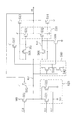
(第1の実施形態)
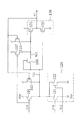
図1は、本発明の第1の実施形態に係る半導体集積回路の回路図である。図1の半導体集積回路は、PMOSトランジスタ(p形MOSFET(metal oxide semiconductor field-effect transistor))101,102,105,107,115と、入力回路120と、出力回路130とを備えている。入力回路120は、NMOSトランジスタ(n形MOSFET)121,122を備えている。出力回路130は、PMOSトランジスタ131と、NMOSトランジスタ132とを備えている。PMOSトランジスタ101,107は、それぞれ第1及び第2のトランジスタとして動作する。PMOSトランジスタ131、及びNMOSトランジスタ132は、それぞれ第1及び第2の駆動トランジスタとして動作する。
【0047】
PMOSトランジスタ101のソースには電源電位VDDが与えられ、ゲートにはクロック信号CLKが与えられている。PMOSトランジスタ101のドレインは、第1のノードN11である。PMOSトランジスタ101は、クロック信号CLKが低論理レベル(以下では、“L”と表記する)のときにオンになり、第1のノードN11を電源電位VDD近傍の電位にプリチャージする。プリチャージされると、ノードN11の電位は高論理レベル(以下では、“H”と表記する)になる。ここでは、高論理レベルが第1の論理レベル、低論理レベルが第2の論理レベルであるとしている。
【0048】
NMOSトランジスタ121のソースには接地電位VSSが与えられ、ゲートには入力信号VI1が与えられている。NMOSトランジスタ122のソースには接地電位VSSが与えられ、ゲートには入力信号VI2が与えられている。NMOSトランジスタ121,122のドレインは、第1のノードN11に接続されている。入力信号VI1,VI2は、クロック信号CLKが“H”のときにのみアクティブ状態になり、クロック信号CLKが“L”のときは“L”に固定される信号である。NMOSトランジスタ121,122は、それぞれ、入力信号VI1,VI2が“H”の時に、第1のノードN11を接地電位VSS近傍の電位(すなわち、“L”)にディスチャージする。すなわち、入力回路120は、OR回路として動作する。
【0049】
PMOSトランジスタ102は、駆動能力(飽和電流量)が小さいPMOSトランジスタであって、そのゲートには図1の回路の出力信号V1、ソースには電源電位VDDが与えられている。PMOSトランジスタ102のドレインは、ノードN11に接続されている。PMOSトランジスタ102は、出力信号V1が“L”の時に、ノードN11を電源電位VDD近傍の電位(すなわち、“H”)にプリチャージする。
【0050】
PMOSトランジスタ102は、NMOSトランジスタ121,122がともにオフであるときに、ノードN11を電源電位VDDの近傍の電位に維持する。一方、NMOSトランジスタ121,122のうちの少なくとも一つがオンになった時に、ノードN11を接地電位VSS近傍の電位に所望の時間内にディスチャージできるようにするため、PMOSトランジスタ102の駆動能力は、NMOSトランジスタ121,122の駆動能力の1/10程度以下に調整してある。
【0051】
PMOSトランジスタ107のソースには電源電位VDDが与えられ、ゲートにはクロック信号CLKが与えられている。PMOSトランジスタ107のドレインは、第2のノードN12となっている。PMOSトランジスタ107は、クロック信号CLKが“L”の時に、ノードN12を電源電位VDD近傍の電位にプリチャージする。第1及び第2のノードN11,N12は、プリチャージラインとも呼ばれる。
【0052】
PMOSトランジスタ105のゲートとドレインとは、ノードN11に接続され、ソースは、PMOSトランジスタ107のドレイン、すなわち、ノードN12に接続されている。ノードN11が接地電位VSS近傍の電位のときは、PMOSトランジスタ105は、オンとなり、ソースとドレインとの間が導通する。ソースとドレインとの間の抵抗が小さくなるので、ノードN12へノードN11の電位が伝えられる。このとき、ノードN12の電位は、ノードN11の電位よりも電圧Vtp1程度高くなる。ここで、電圧Vtp1は、PMOSトランジスタ105のスレッショルド電圧である。ノードN11が電源電位VDD近傍の電位のときは、PMOSトランジスタ105は、オフとなり、ソースとドレインとの間が非導通となる。つまり、ソースとドレインとの間の抵抗が大きくなる。このように、PMOSトランジスタ105は、第1のノードN11と第2のノードN12との間に接続された抵抗素子として動作する。
【0053】
PMOSトランジスタ115は、駆動能力(飽和電流量)が小さいPMOSトランジスタであって、そのゲートには出力信号V1、ソースには電源電位VDDが与えられている。PMOSトランジスタ115のドレインは、ノードN12に接続されている。PMOSトランジスタ115は、出力信号V1が“L”の時に、ノードN12を電源電位VDD近傍の電位にプリチャージする。
【0054】
PMOSトランジスタ115は、PMOSトランジスタ105が非導通であるときに、第2のノードN12を電源電位VDDの近傍の電位に維持する。一方、NMOSトランジスタ121,122のうちの少なくとも一方と、PMOSトランジスタ105とが同時にオンになった時に、ノードN12を接地電位VSS近傍の電位に、所望の時間内にディスチャージできるようにするため、PMOSトランジスタ115の駆動能力は、NMOSトランジスタ121,122及びPMOSトランジスタ105の駆動能力の1/10程度以下に調整してある。
【0055】
PMOSトランジスタ131のソースには電源電位VDDが与えられ、ゲートにはノードが接続されている。PMOSトランジスタ131のドレインにはNMOSトランジスタ132のドレインが接続されている。PMOSトランジスタ131のドレインは、出力ノードとなっていて、出力信号V1を出力している。ノードN12が接地電位VSS近傍の電位の時に、PMOSトランジスタ131は、ソースとドレインとの間が導通し、出力信号V1を“H”にする。
【0056】
NMOSトランジスタ132のソースには接地電位VSSが与えられ、ゲートにはPMOSトランジスタ101のドレイン、すなわち、ノードN11が接続されている。ノードN11が電源電位VDD近傍の電位の時に、NMOSトランジスタ132は、ソースとドレインとの間が導通し、出力信号V1を“L”にする。
【0057】
以下、図1の半導体集積回路の動作について説明する。図1の半導体集積回路は、ダイナミック回路の一種であって、クロック信号CLKが“L”である期間はプリチャージ期間、“H”である期間は評価期間と呼ばれる。図1の半導体集積回路は、評価期間においてアクティブになる入力信号VI1,VI2の論理和を、出力信号V1として出力する。
【0058】
まず、プリチャージ期間における図1の半導体集積回路の動作を詳細に説明する。プリチャージ期間においては、クロック信号CLKが“L”であるので、PMOSトランジスタ101がオンになる。この期間において、入力信号VI1,VI2は、“L”に固定されるので、NMOSトランジスタ121,122はオフになる。すると、ノードN11は電源電位VDD近傍の電位にプリチャージされるので、PMOSトランジスタ105はオフになる。プリチャージ期間においては、PMOSトランジスタ107もオンになるので、ノードN12は電源電位VDD近傍の電位にプリチャージされる。
【0059】
ノードN11とノードN12とが共に電源電位VDD近傍の電位となるので、PMOSトランジスタ131はオフ、NMOSトランジスタ132はオンとなる。したがって、出力信号V1は“L”となる。このとき、PMOSトランジスタ102,115もオンとなる。
【0060】
しかしながら、NMOSトランジスタ121,122及びPMOSトランジスタ105がオフとなっているにもかかわらず、これらのトランジスタのソース−ドレイン間にはサブスレッショルド電流が流れる。このとき流れる電流には、PMOSトランジスタ101,102からNMOSトランジスタ121,122へ流れる電流と、PMOSトランジスタ107,115からPMOSトランジスタ105を経由してNMOSトランジスタ121,122へ流れる電流とがある。このため、プリチャージ期間におけるノードN11,N12のそれぞれの電位VP11,VP12は、いずれも電源電位VDDよりも小さい値となる。
【0061】
このとき、ノードN12の電位VP12は、ノードN11の電位VP11よりも、(VDD−VP11)*R105/(RP+R105)だけ高くなる。PMOSトランジスタ107及び115は、図1のようにソース同士、及びドレイン同士が接続されている。抵抗値RPは、このようにPMOSトランジスタ107及び115が並列に接続された回路の抵抗値であって、これらのトランジスタがともにオンとなっている時の値である。すなわち、PMOSトランジスタ107,115のそれぞれのオン時のソース−ドレイン間抵抗値をr107,r115とすると、RP=r107*r115/(r107+r115)である。抵抗値R105は、NMOSトランジスタ105がオフである時における、そのソース−ドレイン間の抵抗値である。
【0062】
抵抗値R105を、抵抗値RPよりも大きな抵抗値になるようにすることは容易にできるので、PMOSトランジスタ131のゲートの電位を、このゲートを直接ノードN11に接続する場合よりも、電源電位VDDに近い電位にすることができる。したがって、PMOSトランジスタ131のサブスレッショルド電流を削減することができる。
【0063】
一般に、PMOSトランジスタのオフ時のサブスレッショルド電流は、ソース−ゲート間電圧Vgsに対して指数関数的に変化する。すなわち、ドレイン−ソース間電流Ids=Isa*EXP(Vgs/n*Ur)*(1−EXP(−Vgs/Ur))であるので、ゲート電位を電源電位VDDにわずかでも近づければ、効果的にサブスレッショルド電流を削減できる(Ur=kT/q,n=(1+Cd/Cox),k:ボルツマン定数,T:絶対温度,q:電子の電荷,Cd:空乏層容量,Cox:ゲート容量)。
【0064】
言い換えると、PMOSトランジスタ131のゲートを直接ノードN11に接続する場合に比べて、PMOSトランジスタ131のオフ時のソース−ドレイン間の抵抗値R131を高くすることができる。NMOSトランジスタ132のオン時のソース−ドレイン間の抵抗値をr132とすると、出力信号V1の電位はVDD*r132/(R131+r132)であるので、図1の回路によると、出力信号V1の電位をより接地電位VSSに近づけることができる。すなわち、出力信号V1におけるDCノイズを少なくすることができる。
【0065】
次に、評価期間における図1の半導体集積回路の動作を詳細に説明する。評価期間においては、クロック信号CLKが“H”であるので、PMOSトランジスタ101,107がオフになる。プリチャージ期間において出力信号V1は“L”であったので、PMOSトランジスタ102,115はオンであり、ノードN11はPMOSトランジスタ102によって弱くプリチャージされ、ノードN12はPMOSトランジスタ115によって弱くプリチャージされている。
【0066】
評価期間においては、入力信号VI1,VI2がアクティブ状態になる。入力信号VI1,VI2がともに“L”である場合には、NMOSトランジスタ121,122はいずれもオフである。ノードN11は、PMOSトランジスタ102によって弱くプリチャージされているので、電源電位VDD近傍の電位を保つ。ノードN11の電位が高いので、PMOSトランジスタ105はオフとなる。ノードN12は、PMOSトランジスタ115によって弱くプリチャージされているので、電源電位VDD近傍の電位を保つ。
【0067】
ノードN11,N12がいずれも電源電位VDD近傍の電位であるので、PMOSトランジスタ131はオフ、NMOSトランジスタ132はオンとなり、出力信号V1は“L”となる。したがって、PMOS102,115はいずれもオンのままである。
【0068】
しかし、NMOSトランジスタ121,122がオフであるにもかかわらず、これらのトランジスタのドレイン−ソース間にはサブスレッショルド電流が流れる。また、PMOSトランジスタ101,107,105がオフであるにもかかわらず、これらのトランジスタのソース−ドレイン間にはサブスレッショルド電流が流れる。
【0069】
このとき流れる電流には、PMOSトランジスタ101,102からNMOSトランジスタ121,122へ流れる電流と、PMOSトランジスタ107,115からNMOSトランジスタ105を経由してNMOSトランジスタ121,122へ流れる電流とがある。このため、ノードN11,N12のそれぞれの電位VE11,VE12は、いずれも電源電位VDDよりも小さい値となる。
【0070】
このとき、ノードN12の電位VE12は、ノードN11の電位VE11よりも、(VDD−VE11)*R105/(RE1+R105)だけ高くなる。ここで、抵抗値RE1は、図1のようにPMOSトランジスタ107及び115が並列に接続された回路の抵抗値であって、PMOSトランジスタ115のみがオンになっている時の値である。すなわち、PMOSトランジスタ107のオフ時の抵抗値をR107とすると、RE1=R107*r115/(R107+r115)である。
【0071】
抵抗値R105を、抵抗値RE1よりも大きな抵抗値にすることは容易にできるので、PMOSトランジスタ131のゲートの電位を、このゲートを直接ノードN11に接続する場合よりも、電源電位VDDに近い電位にすることができる。したがって、PMOSトランジスタ131のサブスレッショルド電流を削減することができる。
【0072】
言い換えると、PMOSトランジスタ131のゲートを直接ノードN11に接続する場合に比べて、PMOSトランジスタ131のオフ時のソース−ドレイン間の抵抗値R131を高くすることができる。したがって、図1の回路によると、出力信号V1の電位をより接地電位VSSに近づけることができる。すなわち、出力信号V1におけるDCノイズを少なくすることができる。
【0073】
評価期間において入力信号VI1,VI2がともに“H”になった場合には、NMOSトランジスタ121,122はいずれもオンとなる。PMOSトランジスタ102はオンであるが、電流を流す能力が小さいので、ノードN11は、NMOSトランジスタ121,122によって接地電位VSS近傍の電位にディスチャージされる。ノードN11の電位が接地電位VSS近傍の低い電位になるので、PMOSトランジスタ105はオンとなる。PMOSトランジスタ115はオンであるが、電流を流す能力が小さいので、ノードN12はディスチャージされる。ノードN12の電位は、ノードN11の電位よりもPMOSトランジスタ105のスレッショルド電圧Vtp1程度高い電位になる。
【0074】
ノードN11,N12の電位はいずれも“L”であるので、PMOSトランジスタ131がオン、NMOSトランジスタ132がオフとなり、出力信号V1は“H”になる。このため、PMOSトランジスタ102,115がオフになり、ノードN11,N12の電位が更に下がって定常状態になる。PMOSトランジスタ131のゲートの電位がやや高いので、このトランジスタの駆動能力は小さくなるが、特に大きな問題ではない。
【0075】
入力信号VI1,VI2がともに“H”になった場合について説明したが、入力信号VI1,VI2のうちのいずれか一方のみが“H”になった場合についてもほぼ同様であるので、その場合の説明は省略する。
【0076】
以上のように、図1の半導体集積回路は、クロック信号CLKが“L”である期間がプリチャージ期間であり、“H”である期間が評価期間であるダイナミック回路の一種であって、評価期間においてアクティブになる入力信号VI1,VI2の論理和を出力信号V1として出力する。
【0077】
出力ノードを“H”に駆動するPMOSトランジスタ131のゲートは、ノードN11ではなく、ノードN12に接続されている。ノードN11とノードN12との間にはPMOSトランジスタ105が接続され、PMOSトランジスタ105は、ノードN11が電源電位VDD近傍の電位、すなわち、高論理レベル“H”であるときにオフになる(ソース−ドレイン間が高抵抗になる)。入力信号VI1及びVI2が“L”であるときにこれらの信号にDCノイズが重畳すると、NMOSトランジスタ121又は122がオンになって、ノードN11の電位が下がる。このような場合であっても、ノードN12の電位をノードN11の電位よりも高くすることができるので、PMOSトランジスタ131はオフの状態を保つことができる。
【0078】
このように、図1の回路によると、出力信号V1が“L”となる場合に、オフになるPMOSトランジスタ131のサブスレッショルド電流を削減することができるので、出力信号に重畳するDCノイズ、すなわち、所定の論理レベルに対する出力信号のシフトを小さくすることができる。また、入力される信号にDCノイズが含まれている場合においても、DCノイズの少ない信号を出力することができる。したがって、従来のダイナミック回路よりも出力回路におけるリーク電流が少なく、DCノイズに強い半導体集積回路を提供することができる。特に、論理回路を複数段直列に接続するような場合に、図1の半導体集積回路によると、DCノイズの影響を受けて誤動作することが起こりにくくなる。
【0079】
また、図1の回路によると、クロック信号が停止しているときであっても、出力回路のリーク電流を減らすことができるので、待機時における消費電力を抑えることもできる。
【0080】
なお、抵抗素子として、ゲート及びドレインをノードN11に接続し、ソースをノードN12に接続したPMOSトランジスタ105を用いた場合について説明した。同様に、ノードN11の電位が電源電位VDD近傍の電位、すなわち、“H”である時に高抵抗状態となり、このノードの電位が接地電位VSS近傍の電位、すなわち、“L”である時に低抵抗状態になるような素子であれば、PMOSトランジスタ105に代えて他の素子を用いてもよい。
【0081】
また、ノードN11,N12をそれぞれプリチャージするPMOSトランジスタ102及び115のうちのいずれか一方、又は両方を備えないようにしてもよい。
【0082】
(第2の実施形態)
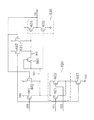
図2は、本発明の第2の実施形態に係る半導体集積回路の回路図である。図2の半導体集積回路は、図1の半導体集積回路において、インバータ240を更に備え、PMOSトランジスタ115を備えないようにしたものである。図2において、PMOSトランジスタ201,202,205,207,231は、それぞれ図1のPMOSトランジスタ101,102,105,107,131と同様のものである。入力回路220及びNMOSトランジスタ232は、それぞれ図1の入力回路120及びNMOSトランジスタ132と同様のものである。また、第1及び第2のノードN21,N22は、それぞれ図1のノードN11,N12に対応している。PMOSトランジスタ205は、抵抗素子として動作する。
【0083】
インバータ240は、PMOSトランジスタ241と、NMOSトランジスタ242とを備えている。PMOSトランジスタ241のソースは電源電位VDDに、ドレインはNMOSトランジスタ242のドレインに、ゲートはノードN21に接続されている。NMOSトランジスタ242のソースは接地電位VSSに、ゲートはノードN21に接続されている。PMOSトランジスタ241のドレインは、インバータ240の出力ノードとなっている。PMOSトランジスタ207のゲートには、クロック信号CLKは入力されず、インバータ240の出力信号が入力されている。
【0084】
次に、プリチャージ期間における図2の半導体集積回路の動作を説明する。プリチャージ期間においては、クロック信号CLKが“L”であるので、PMOSトランジスタ201がオンになる。この期間において、入力信号VI1,VI2は、“L”に固定されるので、NMOSトランジスタ221,222はオフになる。すると、ノードN21は電源電位VDD近傍の電位(すなわち、“H”)にプリチャージされるので、PMOSトランジスタ205はオフになる。
【0085】
ノードN21が“H”のとき、インバータ240の出力信号は“L”であるので、PMOSトランジスタ207はオンになり、ノードN22を電源電位VDD近傍の電位にプリチャージする。
【0086】
ノードN21とノードN22とが共に電源電位VDD近傍の電位となるので、出力信号V2は“L”となる。このとき、PMOSトランジスタ202もオンとなる。このとき流れるサブスレッショルド電流には、PMOSトランジスタ201,202からNMOSトランジスタ221,222へ流れる電流と、PMOSトランジスタ207からPMOSトランジスタ205を経由してNMOSトランジスタ221,222へ流れる電流とがある。このため、プリチャージ期間におけるノードN21,N22のそれぞれの電位VP21,VP22は、いずれも電源電位VDDよりも小さい値となる。
【0087】
このとき、ノードN22の電位VP22は、ノードN21の電位VP21よりも、(VDD−VP21)*R205/(r207+R205)だけ高くなる。ここで、抵抗値r207は、PMOSトランジスタ207がオンであるときのそのソース−ドレイン間の抵抗値であり、抵抗値R205は、NMOSトランジスタ205がオフであるときのそのソース−ドレイン間の抵抗値である。
【0088】
抵抗値R205を、抵抗値r207よりも大きな抵抗値になるようにすることは容易にできるので、PMOSトランジスタ231のゲートの電位を、このゲートを直接ノードN21に接続する場合よりも、電源電位VDDに近い電位にすることができる。したがって、PMOSトランジスタ231のサブスレッショルド電流を削減することができ、このトランジスタのソース−ドレイン間の抵抗値を大きくすることができるので、出力信号V2の電位をより接地電位VSSに近づけることができる。すなわち、図2の回路によると、出力信号V2におけるDCノイズを少なくすることができる。
【0089】
次に、評価期間における図2の半導体集積回路の動作を説明する。評価期間においては、クロック信号CLKが“H”であるので、PMOSトランジスタ201がオフになる。プリチャージ期間において出力信号V2は“L”であったので、PMOSトランジスタ102はオンであり、ノードN11はPMOSトランジスタ102によって弱くプリチャージされている。
【0090】
評価期間においては、入力信号VI1,VI2がアクティブ状態になる。入力信号VI1,VI2がともに“L”である場合には、NMOSトランジスタ221,222はいずれもオフである。ノードN21は、PMOSトランジスタ202によって弱くプリチャージされているので、電源電位VDD近傍の電位を保つ。ノードN21の電位が高いので、PMOSトランジスタ205はオフとなる。ノードN22は、PMOSトランジスタ207によってプリチャージされているので、電源電位VDD近傍の電位を保つ。
【0091】
ノード21,N22がいずれも電源電位VDD近傍の電位であるので、PMOSトランジスタ231はオフ、NMOSトランジスタ232はオンとなり、出力信号V2は“L”となる。したがって、PMOS202はオンのままである。このとき流れるサブスレッショルド電流には、PMOSトランジスタ201,202からNMOSトランジスタ221,222へ流れる電流と、PMOSトランジスタ207からNMOSトランジスタ205を経由してNMOSトランジスタ221,222へ流れる電流とがある。このため、ノードN21,N22のそれぞれの電位VP11,VP12は、いずれも電源電位VDDよりも小さい値となる。
【0092】
このとき、ノードN21,N22の電位は、プリチャージ期間におけるそれぞれの電位VP21,VP22と同様である。したがって、図2の回路によると、出力信号V2におけるDCノイズを少なくすることができる。
【0093】
評価期間において入力信号VI1,VI2がともに“H”になった場合には、NMOSトランジスタ221,222はいずれもオンとなる。PMOSトランジスタ202はオンであるが、電流を流す能力が小さいので、ノードN21は、NMOSトランジスタ221,222によって接地電位VSS近傍の電位(すなわち、“L”)にディスチャージされる。ノードN21の電位が接地電位VSS近傍の低い電位になるので、PMOSトランジスタ205はオンとなる。ノードN21が“L”のとき、PMOSトランジスタ207はオフになるので、、ノードN22はディスチャージされる。そして、ノードN22の電位は、ノードN21の電位よりもPMOSトランジスタ205のスレッショルド電圧Vtp2程度高い電位になる。
【0094】
ノードN21,N22の電位はいずれも“L”であるので、PMOSトランジスタ231がオン、NMOSトランジスタ232がオフとなり、出力信号V2は“H”になる。このため、PMOSトランジスタ202がオフになり、ノードN11の電位が更に下がって定常状態になる。PMOSトランジスタ231のゲートの電位がやや高いので、このトランジスタの駆動能力は小さくなるが、特に大きな問題ではない。
【0095】
入力信号VI1,VI2がともに“H”になった場合について説明したが、入力信号VI1,VI2のうちのいずれか一方のみが“H”になった場合についてもほぼ同様であるので、その場合の説明は省略する。
【0096】
このように、図2の回路によると、出力信号V2を“L”とする場合に、オフになるPMOSトランジスタ231のサブスレッショルド電流を削減することができるので、出力信号に重畳するDCノイズを削減することができる。したがって、従来のダイナミック回路よりも出力回路におけるリーク電流が少なく、DCノイズに強い半導体集積回路を提供することができる。
【0097】
なお、ノードN21をプリチャージするPMOSトランジスタ202を備えないようにしてもよい。
【0098】
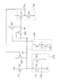
(第3の実施形態)
図3は、本発明の第3の実施形態に係る半導体集積回路の回路図である。図3の半導体集積回路は、図1の半導体集積回路において、NMOSトランジスタ306,308と、インバータ340とを更に備えたものである。図3において、PMOSトランジスタ301,302,305,307,331は、それぞれ図1のPMOSトランジスタ101,102,105,107,131と同様のものである。入力回路320及びNMOSトランジスタ332は、それぞれ図1の入力回路120及びNMOSトランジスタ132と同様のものである。また、第1及び第2のノードN31,N32は、それぞれ図1のノードN11,N12に対応している。PMOSトランジスタ305及びNMOSトランジスタ306は、抵抗素子として動作する。
【0099】
インバータ340は、PMOSトランジスタ341と、NMOSトランジスタ342とを備えており、図2のインバータ240と同様のものである。PMOSトランジスタ341のゲートはノードN31に接続され、ドレインはインバータ340の出力ノードとなっている。
【0100】
NMOSトランジスタ308のソースには接地電位VSSが与えられ、ゲートにはインバータ340の出力信号が入力されている。NMOSトランジスタ308のドレインは、第3のノードN33となっている。NMOSトランジスタ308は、ノードN31が“L”の時に、ノードN33を接地電位VSS近傍の電位にディスチャージする。
【0101】
NMOSトランジスタ306のゲートとドレインとは、ノードN31に接続され、ソースは、NMOSトランジスタ308のドレイン、すなわち、ノードN33に接続されている。ノードN31が電源電位VDD近傍の電位のときは、NMOSトランジスタ306は、オンとなり、ソースとドレインとの間が導通する。ソースとドレインとの間の抵抗が小さくなるので、ノードN33へノードN31の電位が伝えられる。このとき、ノードN33の電位は、ノードN31の電位よりも電圧Vtn3程度低くなる。ここで、電圧Vtn3は、NMOSトランジスタ306のスレッショルド電圧である。ノードN31が接地電位VSS近傍の電位のときは、NMOSトランジスタ306は、オフとなり、ソースとドレインとの間が非導通となる。つまり、ソースとドレインとの間の抵抗が大きくなる。このように、NMOSトランジスタ306は、第1のノードN31と第3のノードN33との間に接続された抵抗素子として動作する。
【0102】
次に、図3の半導体集積回路の動作を、図1の半導体集積回路と異なる点を中心に説明する。プリチャージ期間においては、ノードN31,N32は、図1のノードN11,N12と同様に、いずれも電源電位VDD近傍の電位にプリチャージされる。すると、インバータ340の出力信号は“L”になるので、NMOSトランジスタ308はオフになる。ノードN33の電位が低いとすると、NMOSトランジスタ306はオンになり、ノードN33はノードN31よりも電圧Vtn3程度低い電位にプリチャージされる。
【0103】
評価期間において、入力信号VI1,VI2がともに“L”である場合には、NMOSトランジスタ308,321,322、PMOSトランジスタ301,305,307はオフとなる。これらのトランジスタのソース−ドレイン間にはサブスレッショルド電流が流れるが、図1の場合とほぼ同様に、ノードN31,N32は、プリチャージされた状態を維持する。ノードN33も、ノードN31よりも電圧Vtn3程度低い電位を維持する。
【0104】
評価期間において、入力信号VI1,VI2がともに“H”になった場合には、図1の場合と同様に、ノードN31は、接地電位VSS近傍の電位に、ノードN32は、ノードN31よりもPMOSトランジスタ305のスレッショルド電圧Vtp3程度高い電位にディスチャージされる。ノードN31が“L”になるので、NMOSトランジスタ306がオフになる。また、インバータ340の出力信号は“H”になり、NMOSトランジスタ308がオンになるので、ノードN33はディスチャージされて接地電位VSS程度の電位になる。
【0105】
このとき、PMOSトランジスタ301,302,307,315、NMOSトランジスタ306はオフとなるが、これらのトランジスタのソース−ドレイン間にはサブスレッショルド電流が流れる。このため、ノードN31は接地電位VSSよりも高い電位になる。電流がNMOSトランジスタ306,308を流れるので、ノードN33の電位は、ノードN31の電位VN31よりも、VN31*r308/(r308+R306)だけ低くなる。ここで、R306は、NMOSトランジスタ306がオフであるときのソース−ドレイン間の抵抗値、r308は、NMOSトランジスタ308であるときのソース−ドレイン間の抵抗値である。
【0106】
NMOSトランジスタ306がオフであるときの抵抗値R306を、抵抗値r308よりも大きな抵抗値になるようにすることは容易にできるので、NMOSトランジスタ332のゲートの電位を、このゲートを直接ノードN31に接続する場合よりも、接地電位VSSに近い電位にすることができる。したがって、NMOSトランジスタ332のサブスレッショルド電流を削減することができ、このトランジスタのソース−ドレイン間の抵抗値を大きくすることができるので、出力信号V3の電位をより電源電位VDDに近づけることができる。すなわち、図3の回路によると、出力信号V3におけるDCノイズを少なくすることができる。
【0107】
また、入力信号VI1,VI2のうちの少なくとも一方が“H”であるときに、DCノイズが重畳してその入力信号の電位が下がり、ノードN31の電位が上がっても、ノードN33の電位をノードN31の電位よりも低くすることができるので、NMOSトランジスタ332はオフの状態を保つことができる。
【0108】
このように、図3の回路によると、出力信号V3が“H”となる場合に、オフになるNMOSトランジスタ332のサブスレッショルド電流を削減することができるので、出力信号に重畳するDCノイズ、すなわち、所定の論理レベルに対する出力信号のシフトを小さくすることができる。また、入力される信号にDCノイズが含まれている場合においても、DCノイズの少ない信号を出力することができる。したがって、従来のダイナミック回路よりも出力回路におけるリーク電流が少なく、DCノイズに強い半導体集積回路を提供することができる。
【0109】
なお、抵抗素子として、ゲート及びドレインをノードN31に接続し、ソースをノードN33に接続したNMOSトランジスタ306を用いた場合について説明した。同様に、ノードN31の電位が電源電位VDD近傍の電位、すなわち、“H”である時に低抵抗状態となり、このノードの電位が接地電位VSS近傍の電位、すなわち、“L”である時に高抵抗状態になるような素子を、NMOSトランジスタ306に代えて用いてもよい。
【0110】
また、ノードN32に接続されたトランジスタを図2の回路と同様のものにしてもよい。すなわち、図3において、PMOSトランジスタ307のゲートに、クロック信号CLKに代えてインバータ340の出力信号を与え、PMOSトランジスタ315を備えないようにしてもよい。
【0111】
(第4の実施形態)
図4は、本発明の第4の実施形態に係る半導体集積回路の回路図である。図4の半導体集積回路は、図1の半導体集積回路において、PMOSトランジスタ413を更に備えたものである。図4において、PMOSトランジスタ401,402,405,407,415,431は、それぞれ図1のPMOSトランジスタ101,102,105,107,115,131と同様のものである。入力回路420及びNMOSトランジスタ432は、それぞれ図1の入力回路120及びNMOSトランジスタ132と同様のものである。また、第1及び第2のノードN41,N42は、それぞれ図1のノードN11,N12に対応している。PMOSトランジスタ405は、抵抗素子として動作する。PMOSトランジスタ413は、第3の駆動トランジスタとして動作する。
【0112】
PMOSトランジスタ413のソースには電源電位VDDが与えられ、ドレインは図4の回路の出力ノードであるPMOSトランジスタ431のドレインに接続され、ゲートはノードN41に接続されている。PMOSトランジスタ413は、ノードN41が接地電位VSS近傍の電位(すなわち、“L”)であるときに、図4の回路の出力信号V4を“H”に駆動する。
【0113】
次に、評価期間において、入力信号VI1及びVI2のうちの少なくとも一方が“H”になった場合における図4の半導体集積回路の動作を説明する。この場合には、図1の場合と同様に、ノードN41は接地電位VSS近傍の電位に、ノードN42は、ノードN41よりもPMOSトランジスタ405のスレッショルド電圧Vtp4程度高い電位にディスチャージされる。
【0114】
ノードN42がPMOSトランジスタ405によってディスチャージされるのには時間を要する。また、PMOSトランジスタ413のゲート電位は接地電位VSS近傍の電位まで下がるが、PMOSトランジスタ431のゲート電位は、それよりもPMOSトランジスタ405のスレッショルド電圧Vtp4程度高い電位までしか下がらない。このため、ノードN41が接地電位VSS近傍の電位にディスチャージされると、まず最初にPMOSトランジスタ413がオンになって図4の回路の出力ノードを“H”に駆動し、その後、PMOSトランジスタ431がオンになり、出力ノードを“H”に駆動する。つまり、図4の回路のようにPMOSトランジスタ413を備えることにより、出力信号V4が“H”に変化する際の動作が速くなり、評価期間が開始されてから出力信号が変化するまでの遅延時間を削減することができる。
【0115】
また、図4の回路によると、図1の回路と同様に、PMOSトランジスタ431のサブスレッショルド電流を小さくすることができる。更に、PMOSトランジスタ413,431が並列に接続されているので、これらのトランジスタの駆動能力の和を、PMOSトランジスタ413を備えない場合の駆動トランジスタ(図1のPMOSトランジスタ131等)と同程度にすることができる。例えば、PMOSトランジスタ413,431の大きさを、いずれも図1のPMOSトランジスタ131の1/2にすることができる。したがって、出力ノードを“H”に駆動する駆動トランジスタであるPMOSトランジスタ413,431に流れるリーク電流の和を、従来よりも少なくすることができる。
【0116】
(第5の実施形態)
図5は、本発明の第5の実施形態に係る半導体集積回路の回路図である。図5の半導体集積回路は、図3の半導体集積回路において、PMOSトランジスタ513と、NMOSトランジスタ514とを更に備え、PMOSトランジスタ315を備えないようにしたものである。図5において、PMOSトランジスタ501,502,505,507,531は、それぞれ図3のPMOSトランジスタ301,302,305,307,331と同様のものである。入力回路520、インバータ540、及びNMOSトランジスタ506,508,532は、それぞれ図3の入力回路320、インバータ340、及びNMOSトランジスタ306,308,332と同様のものである。また、第1、第2及び第3のノードN51,N52,及びN53は、それぞれ図3のノードN31,N32,及びN33に対応している。PMOSトランジスタ505及びNMOSトランジスタ506は、抵抗素子として動作する。
【0117】
また、PMOSトランジスタ507のゲートには、クロック信号CLKではなく、インバータ540の出力信号が与えられている。PMOSトランジスタ513の動作等は、図4のPMOSトランジスタ413と同様であるので、その説明を省略する。
【0118】
NMOSトランジスタ514のソースには接地電位VSSが与えられ、ドレインは図5の回路の出力ノードであるPMOSトランジスタ531のドレインに接続され、ゲートはノードN51に接続されている。NMOSトランジスタ514は、ノードN51が電源電位VDD近傍の電位(すなわち、“H”)であるときに、図5の回路の出力信号V5を“L”に駆動する。
【0119】
次に、プリチャージ期間における図5の半導体集積回路の動作を説明する。この場合には、図3の場合と同様に、ノードN51は、電源電位VDD近傍の電位に、ノードN53は、ノードN51よりもNMOSトランジスタ506のスレッショルド電圧Vtn5程度低い電位にプリチャージされる。
【0120】
ノードN53がNMOSトランジスタ506によってプリチャージされるのには時間を要する。また、NMOSトランジスタ514のゲート電位は電源電位VDD近傍の電位まで上がるが、NMOSトランジスタ532のゲート電位は、それよりもNMOSトランジスタ506のスレッショルド電圧Vtn5程度低い電位までしか上がらない。このため、ノードN51が電源電位VDD近傍の電位にプリチャージされると、まず最初にNMOSトランジスタ514がオンになって図5の回路の出力ノードを“L”に駆動し、その後、NMOSトランジスタ532がオンになり、出力ノードを“L”に駆動する。つまり、図5の回路のようにNMOSトランジスタ514を備えることにより、出力信号V5が“L”に変化する際の動作が速くなる。
【0121】
(第6の実施形態)
図6は、本発明の第6の実施形態に係る半導体集積回路の回路図である。図6の半導体集積回路は、図1の半導体集積回路において、入力回路と直列に接続されたNMOSトランジスタ617を更に備えたものである。図6において、PMOSトランジスタ601,602,605,607,615,631は、それぞれ図1のPMOSトランジスタ101,102,105,107,115,131と同様のものである。入力回路620及びNMOSトランジスタ632は、それぞれ図1の入力回路120及びNMOSトランジスタ132と同様のものである。また、第1及び第2のノードN61,N62は、それぞれ図1のノードN11,N12に対応している。PMOSトランジスタ605は、抵抗素子として動作する。
【0122】
NMOSトランジスタ617のドレインには、NMOSトランジスタ621,622のソースが接続されている。NMOSトランジスタ617のソースには接地電位VSSが与えられ、ゲートにはクロック信号CLKが入力されている。NMOSトランジスタ617は、クロック信号CLKが“H”である期間、すなわち、評価期間においてのみ、ソース−ドレイン間が導通する。
【0123】
図1〜図5の半導体集積回路においては、入力信号VI1,VI2は、クロック信号CLKが“H”のときにのみアクティブになり、クロック信号CLKが“L”のときは“L”に固定されるという条件を満たす信号である必要があった。ところが、図6の半導体集積回路によると、NMOSトランジスタ617を備えているので、ノードN61は、クロック信号CLKが“H”である期間においてのみ、ディスチャージされ得る。したがって、入力信号VI1,VI2は、クロック信号CLKが“L”のときは“L”に固定されるという条件を満たす信号である必要がなくなり、入力信号VI1,VI2に対する条件を減らすことができる。
【0124】
(第7の実施形態)
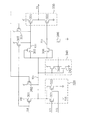
図7は、本発明の第7の実施形態に係る半導体集積回路の回路図である。図7の半導体集積回路は、図1の半導体集積回路において、インバータ740を更に備え、出力回路130を備えないようにした回路を2つ(これらの回路をそれぞれ第1及び第2のダイナミック回路と称する)と、出力回路730とを備えたものである。
【0125】
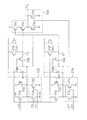
図7において、PMOSトランジスタ701,702,705,707,715は、それぞれ図1のPMOSトランジスタ101,102,105,107,115と同様のものである。入力回路720は、図1の入力回路120と同様のものである。第1及び第2のノードN71,N72は、それぞれ図1のノードN11,N12に対応している。
【0126】
また、PMOSトランジスタ751,752,755,757,765、入力回路770、及びインバータ790は、それぞれPMOSトランジスタ701,702,705,707,715、入力回路720、及びインバータ740と同様のものである。第3及び第4のノードN76,N77は、それぞれ図1のノードN11,N12に対応している。PMOSトランジスタ705,755は、抵抗素子として動作する。
【0127】
インバータ740,790の入力には、それぞれノードN71,N76が接続されている。図1の回路とは異なり、PMOSトランジスタ702,715のゲートには、インバータ740の出力信号が入力されている。PMOSトランジスタ752,765のゲートには、インバータ790の出力信号が入力されている。
【0128】
ノードN71が“H”であるときに、インバータ740の出力信号は“L”になるので、PMOSトランジスタ702はオンになる。つまりこのとき、PMOSトランジスタ702は、ノードN71の論理レベル“H”を維持するように動作する。同様に、ノードN76が“H”であるときに、PMOSトランジスタ752は、ノードN76の論理レベルを維持するように動作する。
【0129】
入力回路720は、NMOSトランジスタ721,722を備え、入力回路770は、NMOSトランジスタ771,772を備えている。NMOSトランジスタ721,722のゲートには、それぞれ入力信号VI1,VI2が入力されている。NMOSトランジスタ771,772のゲートには、それぞれ入力信号VI3,VI4が入力されている。
【0130】
出力回路730は、PMOSトランジスタ731,781と、NMOSトランジスタ732,782とを備えている。第1のダイナミック回路の出力であるノードN71,N72は、それぞれNMOSトランジスタ732、PMOSトランジスタ731のゲートに接続されている。第2のダイナミック回路の出力であるノードN76,N77は、それぞれNMOSトランジスタ782、PMOSトランジスタ781のゲートに接続されている。PMOSトランジスタ781のソースは電源に、ドレインはPMOSトランジスタ731のソースに接続されている。PMOSトランジスタ731のドレインは、NMOSトランジスタ732,782のドレインに接続されている。NMOSトランジスタ732,782のソースは接地されている。PMOSトランジスタ731のドレインは、図7の半導体集積回路の出力ノードとなっている。このように、PMOSトランジスタ731,781と、NMOSトランジスタ732,782とは、1つの論理回路を構成している。
【0131】
ノードN71とN72との論理レベルは等しく、ノードN76とN77との論理レベルは等しいので、出力回路730は、第1のダイナミック回路の出力と第2のダイナミック回路の出力との間のNOR演算の結果を求めて出力していると言える。第1のダイナミック回路は、入力信号VI1とVI2との間のNOR演算の結果を出力し、第2のダイナミック回路は、入力信号VI3とVI4との間のNOR演算の結果を出力する。すなわち、入力信号VI1,VI2,VI3,VI4の論理値をそれぞれA,B,C,Dで表すと、図7の半導体集積回路は、(A NOR B)NOR(C NOR D)=(A OR B)AND(C OR D)を求めて出力する。
【0132】
第1及び第2のダイナミック回路の動作は、図1の半導体集積回路の場合と同様である。すなわち、ノードN71が“H”であるときに、PMOSトランジスタ731のゲートの電位をノードN71よりも高くすることができる。また、ノードN76が“H”であるときに、PMOSトランジスタ781のゲートの電位をノードN76よりも高くすることができる。このため、出力信号V7を“L”とするべきときに、出力信号V7を、PMOSトランジスタ705又は755を備えない場合よりも接地電位VSSに近づけることができる。
【0133】
このように、図7の回路によると、出力信号V7が“L”となる場合に、オフになるPMOSトランジスタ731,781のサブスレッショルド電流を削減することができるので、出力信号に重畳するDCノイズ、すなわち、所定の論理レベルに対する出力信号のシフトを小さくすることができる。したがって、図7のように複雑な出力回路を有する半導体集積回路においても、出力回路におけるリーク電流が少なく、DCノイズに強い半導体集積回路を提供することができる。
【0134】
なお、出力回路730がNOR回路である場合について説明したが、出力回路は、NAND回路等の他の論理回路や、複数の論理回路を組み合わせた回路であってもよい。
【0135】
(第8の実施形態)
図8は、本発明の第8の実施形態に係る半導体集積回路の回路図である。図8の半導体集積回路は、図3の半導体集積回路において、PMOSトランジスタ301,302,315と、入力回路320とを備えないようにした回路に相当する。この回路は、クロック信号を用いないスタティック回路であって、入力信号VIの論理レベルを反転して出力するインバータとして動作する。
【0136】
より具体的には、図8の半導体集積回路は、PMOSトランジスタ805,807と、NMOSトランジスタ806,808と、出力回路830と、インバータ840とを備えている。出力回路830は、PMOSトランジスタ831と、NMOSトランジスタ832とを備え、インバータ840は、PMOSトランジスタ841と、NMOSトランジスタ842とを備えている。
【0137】
図8におけるPMOSトランジスタ805,807,831,841は、それぞれ図3におけるPMOSトランジスタ305,307,331,341と同様のものである。NMOSトランジスタ806,808,832,842は、それぞれNMOSトランジスタ306,308,332,342と同様のものである。図8においては、PMOSトランジスタ805のゲート及びドレイン等は、入力信号VIが直接入力される入力ノードとなっている。第1及び第2のノードN82,N83は、それぞれ図3におけるノードN32,N33に対応している。PMOSトランジスタ805及びNMOSトランジスタ806は、抵抗素子として動作する。PMOSトランジスタ807及びNMOSトランジスタ808は、それぞれ第1及び第2のトランジスタとして動作する。PMOSトランジスタ831及びNMOSトランジスタ832は、それぞれ第1及び第2の駆動トランジスタとして動作する。
【0138】
次に、図8の半導体集積回路の動作について説明する。入力信号VIが“L”である場合には、入力ノードの電位は接地電位VSSの近傍の電位になっている。PMOSトランジスタ805がオンになり、ノードN82の電荷が入力ノードに流れ出すので、ノードN82の電位は、入力ノードの電位よりもPMOSトランジスタ805のスレッショルド電圧Vtp8程度高い電位となる。一方、NMOSトランジスタ806はオフとなる。また、インバータ840の出力ノードは“H”となるので、PMOSトランジスタ807はオフ、NMOSトランジスタ808はオンとなる。このため、ノードN83はNMOSトランジスタ808によってディスチャージされて、接地電位VSS近傍の電位となる。
【0139】
ノードN82,N83の論理レベルはいずれも“L”であるので、PMOSトランジスタ831はオン、NMOSトランジスタ832はオフとなり、出力信号V8は“H”となる。PMOSトランジスタ831のゲートの電位は、入力ノードの電位よりもPMOSトランジスタ805のスレッショルド電圧Vtp8程度高いので、ゲート電位が接地電位VSS近傍の電位のときよりも、PMOSトランジスタ831の駆動能力は小さくなる。
【0140】
ここで、入力ノードが、NMOSトランジスタ回路(図示せず)を介して接地され、PMOSトランジスタ回路(図示せず)を介して電源に接続されているとする。入力信号VIが“L”であるときには、このNMOSトランジスタ回路はオンとなっており、このPMOSトランジスタ回路はオフとなっている。図8の回路の入力ノードと接地線との間におけるこのNMOSトランジスタ回路の抵抗値をrn8、入力ノードと電源との間におけるこのPMOSトランジスタ回路の抵抗値をRp8とし、接地電位VSS=0とすると、入力ノードの電位VINL=VDD*rn8/(Rp8+rn8)となる。
【0141】
このとき、入力ノードからNMOSトランジスタ806,808を経由して接地線に電流が流れる。NMOSトランジスタ806のオフ時のソース−ドレイン間の抵抗値R806、NMOSトランジスタ808のオン時のソース−ドレイン間の抵抗値r808を用いて、ノードN83の電位は、VINL*(r808/(R806+r808))と表される。この電位は、入力ノードの電位VINLよりも、VINL*(R806/(R806+r808))だけ低い。
【0142】
抵抗値R806は、抵抗値r808よりも大きな抵抗値にすることができるので、NMOSトランジスタ832のゲートを直接入力ノードに接続する場合よりも、このトランジスタのゲートの電位を接地電位VSSに近い電位にすることができる。このため、NMOSトランジスタ832のサブスレッショルド電流を削減することができる。すると、NMOSトランジスタ832のソース−ドレイン間の抵抗が大きくなるので、出力信号V8の電位をより電源電位VDDに近い電位にすることができる。すなわち、DCノイズの少ない出力を実現することができる。
【0143】
次に、入力信号VIが“H”である場合の動作について説明する。入力ノードの電位は電源電位VDDの近傍の電位になっている。NMOSトランジスタ806がオンになり、入力ノードからノードN83に電荷が流入するので、ノードN83の電位は、入力ノードの電位よりもNMOSトランジスタ806のスレッショルド電圧Vtn8程度低い電位となる。一方、PMOSトランジスタ805はオフとなる。また、インバータ840の出力ノードは“L”となるので、PMOSトランジスタ807はオン、NMOSトランジスタ808はオフとなる。このため、ノードN82はPMOSトランジスタ807によってチャージされて、電源電位VDD近傍の電位となる。
【0144】
ノードN82,N83の論理レベルはいずれも“H”であるので、PMOSトランジスタ831はオフ、NMOSトランジスタ832はオンとなり、出力信号V8は“L”となる。NMOSトランジスタ832のゲートの電位は、入力ノードの電位よりもNMOSトランジスタ806のスレッショルド電圧Vtn8程度低いので、ゲート電位が電源電位VDD近傍の電位のときよりも、駆動能力が小さくなる。
【0145】
入力信号VIが“L”である場合と同様に、入力ノードが、NMOSトランジスタ回路を介して接地され、PMOSトランジスタ回路を介して電源に接続されているとする。入力信号VIが“H”であるときには、このNMOSトランジスタ回路はオフとなっており、このPMOSトランジスタ回路はオンとなっている。図8の回路の入力ノードと接地線との間におけるこのNMOSトランジスタ回路の抵抗値をRn8、入力ノードと電源との間におけるこのPMOSトランジスタ回路の抵抗値をrp8とし、接地電位VSS=0とすると、入力ノードの電位VINH=VDD*Rn8/(rp8+Rn8)となる。
【0146】
このとき、電源からPMOSトランジスタ807,805を経由して入力ノードに電流が流れる。PMOSトランジスタ805のオフ時のソース−ドレイン間の抵抗値R805、PMOSトランジスタ807のオン時のソース−ドレイン間の抵抗値r807を用いると、ノードN82の電位は、入力ノードの電位VINHよりも、(VDD−VINH)*(R805/(R805+r807))だけ高い。
【0147】
抵抗値R805は、抵抗値r807よりも大きな抵抗値にすることができるので、PMOSトランジスタ831のゲートを直接入力ノードに接続する場合よりも、このトランジスタのゲートの電位を電源電位VDDに近い電位にすることができる。このため、PMOSトランジスタ831のサブスレッショルド電流を削減することができる。すると、PMOSトランジスタ831のソース−ドレイン間の抵抗が大きくなるので、出力信号V8の電位をより接地電位VSSに近い電位にすることができる。すなわち、DCノイズの少ない出力を実現することができる。
【0148】
また、入力信号VIが“H”であるときに、DCノイズが重畳して入力信号VIの電位が下がっても、ノードN82の電位を入力ノードの電位よりも高くすることができるので、PMOSトランジスタ831はオフの状態を保つことができる。また、入力信号VIが“L”であるときに、DCノイズが重畳して入力信号VIの電位が上がっても、ノードN83の電位を入力ノードの電位よりも低くすることができるので、NMOSトランジスタ832はオフの状態を保つことができる。
【0149】
このように、図8の回路によると、出力信号V8が“L”となる場合にオフになるPMOSトランジスタ831、及び出力信号V8が“H”となる場合にオフになるNMOSトランジスタ832のサブスレッショルド電流を削減することができるので、出力信号に重畳するDCノイズ、すなわち、所定の論理レベルに対する出力信号のシフトを小さくすることができる。また、入力される信号にDCノイズが含まれている場合においても、DCノイズの少ない信号を出力することができる。したがって、従来のダイナミック回路よりも出力回路におけるリーク電流が少なく、DCノイズに強い半導体集積回路を提供することができる。
【0150】
なお、図8において、NMOSトランジスタ806及び808を備えず、NMOSトランジスタ832のゲートが入力ノードに接続されるようにしてもよい。この場合は、PMOS831のサブスレッショルド電流を削減することができる。
【0151】
また、図8において、PMOSトランジスタ805及び807を備えず、PMOSトランジスタ831のゲートが入力ノードに接続されるようにしてもよい。この場合は、NMOS832のサブスレッショルド電流を削減することができる。
【0152】
また、抵抗素子として、ゲート及びドレインを入力ノードに接続し、ソースをノードN82に接続したPMOSトランジスタ805を用いた場合について説明した。同様に、入力ノードの電位が電源電位VDD近傍の電位、すなわち、“H”である時に高抵抗状態となり、このノードの電位が接地電位VSS近傍の電位、すなわち、“L”である時に低抵抗状態になるような素子を、PMOSトランジスタ805に代えて用いてもよい。
【0153】
また、抵抗素子として、ゲート及びドレインを入力ノードに接続し、ソースをノードN83に接続したNMOSトランジスタ806を用いた場合について説明した。同様に、入力ノードの電位が電源電位VDD近傍の電位、すなわち、“H”である時に低抵抗状態となり、このノードの電位が接地電位VSS近傍の電位、すなわち、“L”である時に高抵抗状態になるような素子を、NMOSトランジスタ806に代えて用いてもよい。
【0154】
(第9の実施形態)
図8の半導体集積回路は、出力を“H”にする際には、ノードN82をディスチャージするが、PMOS805を経由してディスチャージするので、従来の回路に比べて遅延時間が大きくなってしまう。また、PMOSトランジスタ831のゲートの電位が接地電位VSSよりもPMOSトランジスタ805のスレッショルド電圧Vtp8程度高い電位までしか下がらないので、ゲートの電位が接地電位VSS近傍の電位まで下がる場合に比べて、PMOSトランジスタ831の駆動能力が小さくなってしまう。
【0155】
同様に、図8の半導体集積回路は、出力を“L”にする際には、ノードN83をチャージするが、NMOS806を経由してチャージするので、従来の回路に比べて遅延時間が大きくなってしまう。また、NMOSトランジスタ832のゲートの電位が接地電位VSSよりもNMOSトランジスタ806のスレッショルド電圧Vtn8程度低い電位までしか上がらないので、ゲートの電位が電源電位VDD近傍の電位まで上がる場合に比べて、NMOSトランジスタ832の駆動能力が小さくなってしまう。
【0156】
本実施形態では、このような点を改善した半導体集積回路について説明する。図9は、本発明の第9の実施形態に係る半導体集積回路の回路図である。図9の半導体集積回路は、図8の半導体集積回路において、PMOSトランジスタ913と、NMOSトランジスタ914とを更に備えたものである。
【0157】
図9において、PMOSトランジスタ905,907,931は、それぞれ図8のPMOSトランジスタ805,807,831と同様のものである。NMOSトランジスタ906,908,932及びインバータ940は、それぞれ図8のNMOSトランジスタ806,808,832及びインバータ840と同様のものである。また、第1及び第2のノードN92,N93は、それぞれ図8のノードN82,N83に対応している。PMOSトランジスタ905及びNMOSトランジスタ906は、抵抗素子として動作する。
【0158】
PMOSトランジスタ913のソースには電源電位VDDが与えられ、ドレインは図9の回路の出力ノードであるPMOSトランジスタ931のドレインに接続され、ゲートは入力ノードに接続されている。PMOSトランジスタ913は、入力ノードが接地電位VSS近傍の電位(すなわち、“L”)であるときに、図9の回路の出力信号V9を“H”に駆動する。
【0159】
NMOSトランジスタ914のソースには接地電位VSSが与えられ、ドレインは図9の回路の出力ノードであるPMOSトランジスタ931のドレインに接続され、ゲートは入力ノードに接続されている。NMOSトランジスタ914は、入力ノードが電源電位VDD近傍の電位(すなわち、“H”)であるときに、図9の回路の出力信号V9を“L”に駆動する。
【0160】
次に、図9の半導体集積回路の動作を説明する。入力信号VIが“L”である場合には、入力ノードの電位は接地電位VSSの近傍の電位になっている。図8の場合と同様に、ノードN92は、入力ノードよりもPMOSトランジスタ905のスレッショルド電圧Vtp9程度高い電位にディスチャージされる。
【0161】
ノードN92がPMOSトランジスタ905によってディスチャージされるのには時間を要する。また、PMOSトランジスタ913のゲート電位は接地電位VSS近傍の電位まで下がるが、PMOSトランジスタ931のゲート電位は、それよりもPMOSトランジスタ905のスレッショルド電圧Vtp9程度高い電位までしか下がらない。このため、入力ノードが接地電位VSS近傍の電位にディスチャージされると、まず最初にPMOSトランジスタ913がオンになって図9の回路の出力ノードを“H”に駆動し、その後、PMOSトランジスタ931がオンになり、出力ノードを“H”に駆動する。つまり、図9の回路のようにPMOSトランジスタ913を備えることにより、出力信号V9が“H”に変化する際の動作が速くなり、評価期間が開始されてから出力信号が変化するまでの遅延時間を削減することができる。
【0162】
入力信号VIが“H”である場合には、入力ノードの電位は電源電位VDDの近傍の電位になっている。ノードN93は、入力ノードよりもNMOSトランジスタ906のスレッショルド電圧Vtn9程度低い電位にチャージされる。
【0163】
ノードN93がNMOSトランジスタ906によってチャージされるのには時間を要する。また、NMOSトランジスタ914のゲート電位は電源電位VDD近傍の電位まで上がるが、NMOSトランジスタ932のゲート電位は、それよりもNMOSトランジスタ906のスレッショルド電圧Vtn9程度低い電位までしか上がらない。このため、入力ノードが電源電位VDD近傍の電位にチャージされると、まず最初にNMOSトランジスタ914がオンになって図9の回路の出力ノードを“L”に駆動し、その後、NMOSトランジスタ932がオンになり、出力ノードを“L”に駆動する。つまり、図9の回路のようにNMOSトランジスタ914を備えることにより、出力信号V9が“L”に変化する際の動作が速くなり、評価期間が開始されてから出力信号が変化するまでの遅延時間を削減することができる。
【0164】
なお、インバータ940を備えず、PMOSトランジスタ907及びNMOSトランジスタ908のゲートに出力信号V9を与えるようにしてもよい。
【0165】
(第10の実施形態)
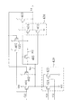
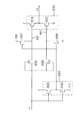
図10は、本発明の第10の実施形態に係る半導体集積回路の回路図である。図10の半導体集積回路は、図8の半導体集積回路において、出力回路830を備えないようにした回路を2つ(これらの回路をそれぞれ第1及び第2のスタティック回路と称する)と、出力回路1030とを備えたものである。
【0166】
図10において、PMOSトランジスタ1005,1007,1031は、それぞれ図8のPMOSトランジスタ805,807,831と同様のものである。NMOSトランジスタ1006,1008,1032は、それぞれ図8のNMOSトランジスタ806,808,832と同様のものである。また、第1及び第2のノードN102,N103は、それぞれ図8のノードN82,N83に対応している。第3及び第4のノードN107,N108は、それぞれ図8のノードN82,N83に対応している。
【0167】
PMOSトランジスタ1055,1057,1081、及びインバータ790は、それぞれPMOSトランジスタ805,807,831、及びインバータ840と同様のものである。NMOSトランジスタ1056,1058,1082は、それぞれ図8のNMOSトランジスタ806,808,832と同様のものである。PMOSトランジスタ1005,1006,1055,1056は、抵抗素子として動作する。
【0168】
出力回路1030は、PMOSトランジスタ1031,1081と、NMOSトランジスタ1032,1082とを備えている。第1のスタティック回路の出力であるノードN102,N103は、それぞれPMOSトランジスタ1031、NMOSトランジスタ1032のゲートに接続されている。第2のスタティック回路の出力であるノードN107,N108は、それぞれPMOSトランジスタ1081、NMOSトランジスタ1082のゲートに接続されている。PMOSトランジスタ1031,1081のソースは電源に、ドレインはNMOSトランジスタ1032のドレインに接続されている。NMOSトランジスタ1032のソースは、NMOSトランジスタ1082のドレインに接続されている。NMOSトランジスタ1082のソースは接地されている。PMOSトランジスタ1031,1081のドレインは、図10の半導体集積回路の出力ノードとなっている。このように、PMOSトランジスタ1031,1081と、NMOSトランジスタ1032,1082とは、1つの論理回路を構成している。
【0169】
第1及び第2のスタティック回路には、それぞれ入力信号VI1,VI2が入力されている。ノードN102とN103との論理レベルは等しく、ノードN107とN108との論理レベルは等しいので、出力回路1030は、第1のスタティック回路の出力と第2のスタティック回路の出力との間のNAND演算の結果を求めて出力していると言える。第1及び第2のスタティック回路は、いずれも入力された信号と同じ論理レベルの信号を出力するので、図10の半導体集積回路は、入力信号VI1,VI2間のNAND演算の結果を出力する。
【0170】
第1及び第2のスタティック回路の動作は、図8の半導体集積回路の場合と同様である。すなわち、入力信号VI1が“H”であるときに、PMOSトランジスタ1031のゲートの電位を、入力信号VI1の電位よりも高く、電源電位VDDに近い電位にすることができる。また、入力信号VI2が“H”であるときに、PMOSトランジスタ1081のゲートの電位を入力信号VI2の電位よりも高くすることができる。このため、出力信号V10を“L”とするべきときに、出力信号V10を、PMOSトランジスタ1005又は1055を備えない場合よりも接地電位VSSに近づけることができる。
【0171】
同様に、入力信号VI1が“L”であるときに、NMOSトランジスタ1032のゲートの電位を、入力信号VI1の電位よりも低く、接地電位VDDに近い電位にすることができる。また、入力信号VI2が“L”であるときに、NMOSトランジスタ1082のゲートの電位を入力信号VI2の電位よりも低くすることができる。このため、出力信号V10を“H”とするべきときに、出力信号V10を、PMOSトランジスタ1005又は1055を備えない場合よりも電源電位VDDに近づけることができる。
【0172】
このように、図10の回路によると、出力信号V10が“L”となる場合に、オフになるPMOSトランジスタ1031,1081のサブスレッショルド電流を削減することができるので、出力信号に重畳するDCノイズ、すなわち、所定の論理レベルに対する出力信号のシフトを小さくすることができる。したがって、図10のように複雑な出力回路を有する半導体集積回路においても、出力回路におけるリーク電流が少なく、DCノイズに強い半導体集積回路を提供することができる。
【0173】
なお、出力回路1030がNAND回路である場合について説明したが、出力回路は、NOR回路等の他の論理回路や、複数の論理回路を組み合わせた回路であってもよい。
【0174】
また、以上の実施形態において、全てのトランジスタの導電型及び信号の論理を逆にしてもよい。すなわち、図1〜図10において、全てのPMOSトランジスタをNMOSトランジスタに、全てのNMOSトランジスタをPMOSトランジスタに変更し、電源電位VDDと接地電位VSSとを入れ換え、全ての信号の論理を逆転した構成にしてもよい。このときには、低論理レベルが第1の論理レベル、高論理レベルが第2の論理レベルであるとする。
【0175】
また、MOSトランジスタに代えて、これ以外のトランジスタ等のデバイスを用いてもよい。
【0176】
また、第1の抵抗素子としてPMOSトランジスタ、第2の抵抗素子としてNMOSトランジスタを用いる場合について説明したが、これには限らない。すなわち、2つの端子間の電位差が大きいときには端子間が低抵抗になり、小さいときには端子間が高抵抗になるような素子であれば、これらの抵抗素子として用いてもよい。
【0177】
また、第1〜第7の実施形態において、入力回路が並列に接続された2つのNMOSトランジスタを備え、2つの入力信号VI1,VI2の論理和に従って第1のノードの電位が変化する場合について説明したが、入力回路の構成はこれ以外の論理演算を実現するものであってもよい。すなわち、入力信号の数が2より多くてもよいし、複数の入力信号の論理積や、異なる論理積の間の論理和等に従って第1のノードの電位が変化するようにしてもよい。
【0178】
【発明の効果】
以上のように、本発明によると、入力される信号にDCノイズが含まれている場合においても、DCノイズの少ない信号を出力する半導体集積回路を得ることができる。したがって、回路を複数直列に接続しても、DCノイズが増幅されて大きくなることがなく、回路が誤動作しないようにすることができる。
【0179】
また、ダイナミック回路において、入力されるクロック信号が停止しているときにも出力回路のリーク電流を減らすことができるので、待機時における回路全体の消費電力を抑えることもできる。
【図面の簡単な説明】
【図1】本発明の第1の実施形態に係る半導体集積回路の回路図である。
【図2】本発明の第2の実施形態に係る半導体集積回路の回路図である。
【図3】本発明の第3の実施形態に係る半導体集積回路の回路図である。
【図4】本発明の第4の実施形態に係る半導体集積回路の回路図である。
【図5】本発明の第5の実施形態に係る半導体集積回路の回路図である。
【図6】本発明の第6の実施形態に係る半導体集積回路の回路図である。
【図7】本発明の第7の実施形態に係る半導体集積回路の回路図である。
【図8】本発明の第8の実施形態に係る半導体集積回路の回路図である。
【図9】本発明の第9の実施形態に係る半導体集積回路の回路図である。
【図10】本発明の第10の実施形態に係る半導体集積回路の回路図である。
【図11】従来のダイナミック型の半導体集積回路の例を示す回路図である。
【図12】従来のスタティック型の半導体集積回路の例を示す回路図である。
【符号の説明】
101,201,301,401,501,601,701,751 PMOSトランジスタ(第1のトランジスタ)
102,202,302,402,502,602,702,752 PMOSトランジスタ(第3のトランジスタ)
105,205,305,405,505,605,705,755,805,905,1005,1055 PMOSトランジスタ(第1の抵抗素子)
306,506,806,906,1006,1056 NMOSトランジスタ(第2の抵抗素子)
107,207,307,407,507,607,707,757 PMOSトランジスタ(第2のトランジスタ)
115,315,415,615,715,765 PMOSトランジスタ(第3のトランジスタ)
120,220,320,420,520,620,720,770 入力回路131,231,331,431,531,631,731,781,831,931,1031,1081 PMOSトランジスタ(第1の駆動トランジスタ)
132,232,332,432,532,632,732,782,832,932,1032,1082 NMOSトランジスタ(第2の駆動トランジスタ)
240,340,540,740,790,840,940,1040,1090 インバータ
308,508 NMOSトランジスタ(第3のトランジスタ)
413,513,913 PMOSトランジスタ(第3の駆動トランジスタ)
514,914 NMOSトランジスタ(第3の駆動トランジスタ)
617 NMOSトランジスタ(第3のトランジスタ)
807,907,1007,1057 PMOSトランジスタ(第1のトランジスタ)
808,908,1008,1058 NMOSトランジスタ(第2のトランジスタ)[0001]
BACKGROUND OF THE INVENTION
The present invention relates to a semiconductor integrated circuit, and more particularly to a logic circuit.
[0002]
[Prior art]
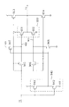
In recent years, semiconductor integrated circuits have been miniaturized to realize high-speed operation, area saving, low power consumption, and the like. When the process is miniaturized and the gate length of the transistor is shortened, there is a merit that the amount of drain current per unit gate width of the transistor flowing when the transistor is on increases. On the other hand, there is a problem in that a drain-source leakage current (hereinafter referred to as a subthreshold current) that flows when the transistor is off increases. The increase rate of the subthreshold current accompanying the miniaturization is larger than the increase rate of the drain current amount that flows when the transistor is in the ON state.
[0003]
FIG. 11 is a circuit diagram showing an example of a conventional dynamic semiconductor integrated circuit. The circuit in FIG. 11 includes
[0004]
A period in which the clock signal CLK is “L” (low logic level) is a precharge period. During this period, the
[0005]
A period in which the clock signal CLK is “H” (high logic level) is an evaluation period. During this period, the input signals VI1 and VI2 are active. When one of the input signals VI1 and VI2 becomes “H”, the node N211 is discharged and the output signal V21 becomes “H”. When the input signals VI1 and VI2 are both “L”, the node N211 is not discharged and the output signal V21 is “L”. At this time, the
[0006]
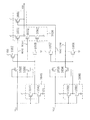
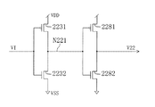
FIG. 12 is a circuit diagram showing an example of a conventional static type semiconductor integrated circuit. The circuit of FIG. 12 operates as a buffer circuit in which inverters are connected in two stages in series. The circuit in FIG. 12 includes an inverter having a
[0007]
[Problems to be solved by the invention]
In the dynamic circuit configured as shown in FIG. 14, a case will be described in which the subthreshold current that flows when the transistor is off cannot be ignored compared to the drain current that flows when the transistor is on.
[0008]
In the evaluation period, even if the input signals VI1 and VI2 are both “L”, the subthreshold current flows through the
[0009]
Here, if the voltage Vd is smaller than the threshold voltage Vt of the PMOS transistor 2131 (the voltage between the gate and the source when the transistor switches from the off state to the on state), the
[0010]
If the voltage Vd is larger than the threshold voltage Vt of the
[0011]
Even in the precharge period, if a subthreshold current flows through the
[0012]
Since the subthreshold current has a property of increasing exponentially with respect to the voltage Vgs between the gate and the source of the transistor, when the gate-source voltage Vgs of the
[0013]
Thus, when the subthreshold current cannot be ignored, the potential shift of the output signal V21, that is, the output DC noise becomes so large that it cannot be ignored. In particular, when the DC noise included in the output signal is larger than the DC noise included in the input signal, the DC noise is amplified.
[0014]
Such a phenomenon is described in the document Atila Alvandpour et. Al. 2001 Symposium on VLSI Circuits Digest of Technical Papers 3-4, “A conditional Keeper Technique for Sub-0.13 μ Wide Dynamic Gates”.
[0015]
If a plurality of circuits that amplify and output the DC noise included in the input signal are connected in series, the DC noise gradually increases and eventually the circuit malfunctions. Even if the circuit does not amplify DC noise, if the voltage Vd or the potential shift Vdo of the output signal V21 becomes a large value, the leakage current flowing between the power supply and the ground line exponentially functions. Since it becomes large, there is a problem that power consumption becomes large when the transistor is off.
[0016]
Even in the static circuit configured as shown in FIG. 15, the same problem occurs when the subthreshold current that flows when the transistor is off cannot be ignored compared to the drain current that flows when the transistor is on. is there.
[0017]
That is, since the subthreshold current flows through the
[0018]
An object of the present invention is to provide a semiconductor integrated circuit that outputs a signal with low DC noise.
[0019]
[Means for Solving the Problems]
In order to solve the above-mentioned problem, the means taken by the invention of claim 1 is a semiconductor integrated circuit, a first transistor for setting a first node to a first logic level according to a clock signal, and a response according to an input signal. An input circuit for setting the first node to a second logic level different from the first logic level, and a second node when the first node becomes the first logic level. A second transistor configured to be at a logic level of 1 and connected between the first node and the second node and having resistance when the first node is at the first logic level Whether or not the first resistance element whose value increases and the resistance value decreases at the second logic level, the second node as an input, and the output node at the first logic level First drive transistor for controlling If, as input said first same logic level signal and a node is the output node that includes a second driving transistor for controlling whether to said second logic level.
[0020]
According to the first aspect of the present invention, since the first resistance element is provided, the absolute value of the gate-source voltage of the transistor can be reduced when the first driving transistor is turned off. For this reason, in the dynamic circuit operating in synchronization with the clock, the subthreshold current of the first drive transistor can be reduced, so that DC noise included in the output signal can be reduced.
[0021]
According to a second aspect of the present invention, in the semiconductor integrated circuit according to the first aspect, the second transistor sets the second node to the first logic level in accordance with the clock signal. .
[0022]
The semiconductor integrated circuit according to claim 1 further includes an inverter that inverts and outputs a logic level of the first node, and the second transistor is an output of the inverter. A signal is input and when the first node is at the first logic level, the second node is at the first logic level.
[0023]
According to a fourth aspect of the present invention, in the semiconductor integrated circuit according to the first aspect, the output node is an input, and the second node is the first logic level when the output node is at the second logic level. A third transistor having a logic level of is further provided.
[0024]
According to a fifth aspect of the present invention, in the semiconductor integrated circuit according to the first aspect, when the output node is an input and the output node is at the second logic level, the first node is the first logic level. A third transistor having a logic level of is further provided.
[0025]
According to a sixth aspect of the present invention, in the semiconductor integrated circuit according to the first aspect, an inverter for inverting and outputting a logic level of the first node, and an output signal of the inverter as inputs, And a third transistor that operates to maintain the logic level when the node is at the first logic level.
[0026]
According to a seventh aspect of the present invention, in the semiconductor integrated circuit according to the first aspect, the third drive for controlling whether or not the first node is an input and the output node is the first logic level. A transistor is further provided.
[0027]
According to an eighth aspect of the present invention, in the semiconductor integrated circuit according to the first aspect, the first resistance element is a transistor having a gate and a drain connected to each other.
[0028]
According to a ninth aspect of the present invention, in the semiconductor integrated circuit according to the first aspect, an inverter for inverting and outputting a logic level of the first node, and an output signal of the inverter as inputs, A third transistor that causes a third node to be at the second logic level when the node is at the second logic level, and connected between the first node and the third node And a second resistance element that decreases in resistance when the first node is at the first logic level and increases in resistance when the first node is at the second logic level, The second driving transistor has the third node as an input.
[0029]
According to the ninth aspect of the invention, since the second resistance element is provided, the absolute value of the gate-source voltage of the transistor can be reduced when the second driving transistor is turned off. For this reason, since the subthreshold current of the second drive transistor can be reduced, the DC noise included in the output signal can be reduced.
[0030]
According to a tenth aspect of the present invention, in the semiconductor integrated circuit according to the ninth aspect, the third drive for controlling whether or not the first node is an input and the output node is the second logic level. A transistor is further provided.
[0031]
According to an eleventh aspect of the present invention, in the semiconductor integrated circuit according to the ninth aspect, the second resistance element is a transistor in which a gate and a drain are connected.
[0032]
According to a twelfth aspect of the present invention, in the semiconductor integrated circuit according to the first aspect, when the clock signal is input and connected in series with the input circuit, the clock signal is at the first logic level. A third transistor that is conductive is further provided.
[0033]
A thirteenth aspect of the invention includes a plurality of the semiconductor integrated circuits according to the first aspect, and the first and second driving transistors of the plurality of semiconductor integrated circuits constitute one logic circuit. It is.
[0034]
According to a fourteenth aspect of the present invention, as a semiconductor integrated circuit, when an input node is at a first logic level, a first transistor that causes the first node to be at the first logic level, and the input A resistance value increases when the input node is at the first logic level, and is a second logic level different from the first logic level. The second logic level is connected between the node and the first node. A first resistance element whose resistance value is sometimes reduced, a first driving transistor for controlling whether or not the first node is an input and an output node is the first logic level, and the input node And a second drive transistor for controlling whether or not the output node is set to the second logic level.
[0035]
According to the fourteenth aspect of the invention, since the first resistance element is provided, the absolute value of the gate-source voltage of the transistor can be reduced when the first driving transistor is turned off. For this reason, since the subthreshold current of the first drive transistor can be reduced, DC noise included in the output signal can be reduced.
[0036]
The invention of claim 15 is the semiconductor integrated circuit according to claim 14, further comprising an inverter that inverts and outputs a logic level of the input node, wherein the first transistor outputs an output signal of the inverter. Input, and when the input node is at the first logic level, the first node is at the first logic level.
[0037]
According to a sixteenth aspect of the present invention, there is provided the semiconductor integrated circuit according to the fourteenth aspect, wherein the input node is an input and the output node is controlled to be the first logic level. Is further provided.
[0038]
According to a seventeenth aspect of the present invention, in the semiconductor integrated circuit according to the fourteenth aspect, the first resistance element is a transistor in which a gate and a drain are connected.
[0039]
Further, an invention according to claim 18 is the semiconductor integrated circuit according to claim 14, wherein an inverter that inverts and outputs a logic level of the input node and an output signal of the inverter are input, and the input node is the first node. A second transistor that causes the second node to be at the second logic level when at a logic level of 2 and connected between the input node and the second node; A second resistance element that decreases in resistance when the first logic level is set and increases in resistance when the second logic level is set; The second node is input.
[0040]
According to a nineteenth aspect of the present invention, there is provided the semiconductor integrated circuit according to the eighteenth aspect, wherein the input node is an input and the output node is controlled to be the second logic level. Is further provided.
[0041]
According to a twentieth aspect of the present invention, in the semiconductor integrated circuit according to the eighteenth aspect, the second resistance element is a transistor having a gate and a drain connected to each other.
[0042]
According to a twenty-first aspect of the present invention, a plurality of the semiconductor integrated circuits according to the fourteenth aspect are provided, and the first and second drive transistors of the plurality of semiconductor integrated circuits constitute one logic circuit. It is.
[0043]
According to a twenty-second aspect of the present invention, in the semiconductor integrated circuit according to any one of the first to twenty-first aspects, the first potential is a high logic level and the second potential is a low logic level. Features.
[0044]
According to a twenty-third aspect of the present invention, in the semiconductor integrated circuit according to any one of the first to twenty-first aspects, the first potential is at a low logic level and the second potential is at a high logic level. Features.
[0045]
DETAILED DESCRIPTION OF THE INVENTION
Hereinafter, embodiments of the present invention will be described with reference to the drawings.
[0046]
(First embodiment)
FIG. 1 is a circuit diagram of a semiconductor integrated circuit according to the first embodiment of the present invention. The semiconductor integrated circuit of FIG. 1 includes PMOS transistors (p-type MOSFETs (metal oxide semiconductor field-effect transistors)) 101, 102, 105, 107, and 115, an
[0047]
The source of the
[0048]
The ground potential VSS is applied to the source of the
[0049]
The
[0050]
The
[0051]
The source of the
[0052]
The gate and drain of the
[0053]
The
[0054]
The
[0055]
The source of the
[0056]
The ground potential VSS is applied to the source of the NMOS transistor 132, and the drain of the
[0057]
The operation of the semiconductor integrated circuit of FIG. 1 will be described below. The semiconductor integrated circuit in FIG. 1 is a kind of dynamic circuit, and a period in which the clock signal CLK is “L” is called a precharge period, and a period in which the clock signal CLK is “H” is called an evaluation period. The semiconductor integrated circuit of FIG. 1 outputs the logical sum of the input signals VI1 and VI2 that become active during the evaluation period as the output signal V1.
[0058]
First, the operation of the semiconductor integrated circuit of FIG. 1 in the precharge period will be described in detail. In the precharge period, since the clock signal CLK is “L”, the
[0059]
Since the node N11 and the node N12 are both near the power supply potential VDD, the
[0060]
However, although the
[0061]
At this time, the potential VP12 of the node N12 is higher than the potential VP11 of the node N11 by (VDD−VP11) * R105 / (RP + R105). As shown in FIG. 1, the
[0062]
Since the resistance value R105 can be easily set to a resistance value larger than the resistance value RP, the potential of the gate of the
[0063]
In general, the subthreshold current when the PMOS transistor is off varies exponentially with respect to the source-gate voltage Vgs. That is, since the drain-source current Ids = Isa * EXP (Vgs / n * Ur) * (1-EXP (−Vgs / Ur)), it is effective if the gate potential is slightly brought close to the power supply potential VDD. The subthreshold current can be reduced (Ur = kT / q, n = (1 + Cd / Cox), k: Boltzmann constant, T: absolute temperature, q: electron charge, Cd: depletion layer capacitance, Cox: gate capacitance).
[0064]
In other words, the resistance value R131 between the source and the drain when the
[0065]
Next, the operation of the semiconductor integrated circuit of FIG. 1 during the evaluation period will be described in detail. In the evaluation period, since the clock signal CLK is “H”, the
[0066]
In the evaluation period, the input signals VI1 and VI2 are in an active state. When the input signals VI1 and VI2 are both “L”, the
[0067]
Since the nodes N11 and N12 are both near the power supply potential VDD, the
[0068]
However, although the
[0069]
The current flowing at this time includes a current flowing from the
[0070]
At this time, the potential VE12 of the node N12 is higher than the potential VE11 of the node N11 by (VDD−VE11) * R105 / (RE1 + R105). Here, the resistance value RE1 is a resistance value of a circuit in which the
[0071]
Since the resistance value R105 can be easily set to a resistance value larger than the resistance value RE1, the potential of the gate of the
[0072]
In other words, the resistance value R131 between the source and the drain when the
[0073]
When the input signals VI1 and VI2 are both “H” during the evaluation period, both the
[0074]
Since the potentials of the nodes N11 and N12 are both “L”, the
[0075]
The case where both of the input signals VI1 and VI2 are “H” has been described. However, since only one of the input signals VI1 and VI2 is “H”, the same is true. Description is omitted.
[0076]
As described above, the semiconductor integrated circuit of FIG. 1 is a kind of dynamic circuit in which the period in which the clock signal CLK is “L” is the precharge period and the period in which the clock signal CLK is “H” is the evaluation period. The logical sum of the input signals VI1 and VI2 that become active during the period is output as the output signal V1.
[0077]
The gate of the
[0078]
As described above, according to the circuit of FIG. 1, when the output signal V1 becomes “L”, the subthreshold current of the
[0079]
Further, according to the circuit of FIG. 1, since the leakage current of the output circuit can be reduced even when the clock signal is stopped, power consumption during standby can be suppressed.
[0080]
Note that the case where the
[0081]
Further, either one or both of the
[0082]
(Second Embodiment)
FIG. 2 is a circuit diagram of a semiconductor integrated circuit according to the second embodiment of the present invention. The semiconductor integrated circuit of FIG. 2 is the same as the semiconductor integrated circuit of FIG. 1 except that it further includes an
[0083]
The
[0084]
Next, the operation of the semiconductor integrated circuit in FIG. 2 during the precharge period will be described. In the precharge period, since the clock signal CLK is “L”, the
[0085]
When the node N21 is “H”, since the output signal of the
[0086]
Since both the node N21 and the node N22 have a potential in the vicinity of the power supply potential VDD, the output signal V2 becomes “L”. At this time, the
[0087]
At this time, the potential VP22 of the node N22 is higher than the potential VP21 of the node N21 by (VDD−VP21) * R205 / (r207 + R205). Here, the resistance value r207 is the resistance value between the source and the drain when the
[0088]
Since the resistance value R205 can be easily set to a resistance value larger than the resistance value r207, the potential of the gate of the
[0089]
Next, the operation of the semiconductor integrated circuit in FIG. 2 during the evaluation period will be described. In the evaluation period, since the clock signal CLK is “H”, the
[0090]
In the evaluation period, the input signals VI1 and VI2 are in an active state. When the input signals VI1 and VI2 are both “L”, the
[0091]
Since the nodes 21 and N22 are both near the power supply potential VDD, the
[0092]
At this time, the potentials of the nodes N21 and N22 are the same as the respective potentials VP21 and VP22 in the precharge period. Therefore, according to the circuit of FIG. 2, DC noise in the output signal V2 can be reduced.
[0093]
When the input signals VI1 and VI2 are both “H” during the evaluation period, the
[0094]
Since the potentials of the nodes N21 and N22 are both “L”, the
[0095]
The case where both of the input signals VI1 and VI2 are “H” has been described. However, since only one of the input signals VI1 and VI2 is “H”, the same is true. Description is omitted.
[0096]
As described above, according to the circuit of FIG. 2, when the output signal V2 is set to “L”, the subthreshold current of the
[0097]
The
[0098]
(Third embodiment)
FIG. 3 is a circuit diagram of a semiconductor integrated circuit according to the third embodiment of the present invention. The semiconductor integrated circuit of FIG. 3 further includes
[0099]
The
[0100]
The ground potential VSS is applied to the source of the
[0101]
The gate and drain of the
[0102]
Next, the operation of the semiconductor integrated circuit of FIG. 3 will be described focusing on differences from the semiconductor integrated circuit of FIG. In the precharge period, the nodes N31 and N32 are both precharged to a potential in the vicinity of the power supply potential VDD, similarly to the nodes N11 and N12 in FIG. Then, since the output signal of the
[0103]
In the evaluation period, when the input signals VI1, VI2 are both “L”, the
[0104]
When both of the input signals VI1 and VI2 become “H” during the evaluation period, the node N31 is at a potential near the ground potential VSS, and the node N32 is more PMOS than the node N31, as in FIG. The
[0105]
At this time, the
[0106]
Since the resistance value R306 when the
[0107]
Further, when at least one of the input signals VI1 and VI2 is “H”, even if DC noise is superimposed and the potential of the input signal is lowered and the potential of the node N31 is raised, the potential of the node N33 is changed to the node. Since the potential can be lower than the potential of N31, the
[0108]
As described above, according to the circuit of FIG. 3, when the output signal V3 becomes “H”, the subthreshold current of the
[0109]
The case where the
[0110]
Further, the transistor connected to the node N32 may be the same as the circuit in FIG. That is, in FIG. 3, the output signal of the
[0111]
(Fourth embodiment)
FIG. 4 is a circuit diagram of a semiconductor integrated circuit according to the fourth embodiment of the present invention. The semiconductor integrated circuit of FIG. 4 further includes a
[0112]
The source of the
[0113]
Next, the operation of the semiconductor integrated circuit of FIG. 4 when at least one of the input signals VI1 and VI2 becomes “H” in the evaluation period will be described. In this case, similarly to the case of FIG. 1, the node N41 is discharged to a potential near the ground potential VSS, and the node N42 is discharged to a potential higher than the node N41 by about the threshold voltage Vtp4.
[0114]
It takes time for the node N42 to be discharged by the
[0115]
Further, according to the circuit of FIG. 4, the subthreshold current of the
[0116]
(Fifth embodiment)
FIG. 5 is a circuit diagram of a semiconductor integrated circuit according to the fifth embodiment of the present invention. The semiconductor integrated circuit of FIG. 5 is the same as the semiconductor integrated circuit of FIG. 3 except that it further includes a
[0117]
Further, the output signal of the
[0118]
The ground potential VSS is applied to the source of the
[0119]
Next, the operation of the semiconductor integrated circuit in FIG. 5 during the precharge period will be described. In this case, similarly to the case of FIG. 3, the node N51 is precharged to a potential near the power supply potential VDD, and the node N53 is precharged to a potential lower than the node N51 by about the threshold voltage Vtn5.
[0120]
It takes time for the node N53 to be precharged by the
[0121]
(Sixth embodiment)
FIG. 6 is a circuit diagram of a semiconductor integrated circuit according to the sixth embodiment of the present invention. The semiconductor integrated circuit of FIG. 6 further includes an
[0122]
The sources of the
[0123]
1 to 5, the input signals VI1 and VI2 are active only when the clock signal CLK is “H”, and are fixed to “L” when the clock signal CLK is “L”. It was necessary to be a signal that satisfies the condition. However, since the semiconductor integrated circuit of FIG. 6 includes the
[0124]
(Seventh embodiment)
FIG. 7 is a circuit diagram of a semiconductor integrated circuit according to the seventh embodiment of the present invention. The semiconductor integrated circuit of FIG. 7 includes two circuits that are further provided with an
[0125]
In FIG. 7,
[0126]
The
[0127]
Nodes N71 and N76 are connected to the inputs of the
[0128]
When the node N71 is “H”, the output signal of the
[0129]
The
[0130]
The
[0131]
Since the logic levels of the nodes N71 and N72 are equal and the logic levels of the nodes N76 and N77 are equal, the
[0132]
The operations of the first and second dynamic circuits are the same as those of the semiconductor integrated circuit of FIG. That is, when the node N71 is “H”, the potential of the gate of the
[0133]
As described above, according to the circuit of FIG. 7, when the output signal V7 becomes “L”, the subthreshold currents of the
[0134]
Although the case where the
[0135]
(Eighth embodiment)
FIG. 8 is a circuit diagram of a semiconductor integrated circuit according to the eighth embodiment of the present invention. The semiconductor integrated circuit of FIG. 8 corresponds to a circuit in which the
[0136]
More specifically, the semiconductor integrated circuit of FIG. 8 includes
[0137]
The
[0138]
Next, the operation of the semiconductor integrated circuit of FIG. 8 will be described. When the input signal VI is “L”, the potential of the input node is near the ground potential VSS. Since the
[0139]
Since the logic levels of the nodes N82 and N83 are both “L”, the
[0140]
Here, it is assumed that the input node is grounded via an NMOS transistor circuit (not shown) and connected to a power source via a PMOS transistor circuit (not shown). When the input signal VI is “L”, the NMOS transistor circuit is on and the PMOS transistor circuit is off. When the resistance value of the NMOS transistor circuit between the input node and the ground line of the circuit of FIG. 8 is rn8, the resistance value of the PMOS transistor circuit between the input node and the power supply is Rp8, and the ground potential VSS = 0. The potential of the input node VINL = VDD * rn8 / (Rp8 + rn8).
[0141]
At this time, a current flows from the input node to the ground line via the
[0142]
Since the resistance value R806 can be larger than the resistance value r808, the potential of the gate of this transistor is closer to the ground potential VSS than when the gate of the
[0143]
Next, the operation when the input signal VI is “H” will be described. The potential of the input node is near the power supply potential VDD. Since the
[0144]
Since the logic levels of the nodes N82 and N83 are both “H”, the
[0145]
As in the case where the input signal VI is “L”, it is assumed that the input node is grounded via the NMOS transistor circuit and connected to the power supply via the PMOS transistor circuit. When the input signal VI is “H”, the NMOS transistor circuit is off and the PMOS transistor circuit is on. The resistance value of the NMOS transistor circuit between the input node and the ground line of the circuit of FIG. 8 is Rn8, the resistance value of the PMOS transistor circuit between the input node and the power supply is rp8, and the ground potential VSS = 0. Therefore, the potential of the input node VINH = VDD * Rn8 / (rp8 + Rn8).
[0146]
At this time, a current flows from the power source to the input node via the
[0147]
Since the resistance value R805 can be larger than the resistance value r807, the potential of the gate of this transistor is closer to the power supply potential VDD than when the gate of the
[0148]
Further, when the input signal VI is “H”, the potential of the node N82 can be made higher than the potential of the input node even if DC noise is superimposed and the potential of the input signal VI is lowered. Therefore, the
[0149]
As described above, according to the circuit of FIG. 8, the sub-threshold of the
[0150]
In FIG. 8, the
[0151]
In FIG. 8, the
[0152]
Further, the case where the
[0153]
Further, the case where the
[0154]
(Ninth embodiment)
The semiconductor integrated circuit of FIG. 8 discharges the node N82 when the output is set to “H”, but discharges it via the
[0155]
Similarly, in the semiconductor integrated circuit of FIG. 8, when the output is set to “L”, the node N83 is charged, but since it is charged via the
[0156]
In the present embodiment, a semiconductor integrated circuit in which such points are improved will be described. FIG. 9 is a circuit diagram of a semiconductor integrated circuit according to the ninth embodiment of the present invention. The semiconductor integrated circuit of FIG. 9 further includes a
[0157]
In FIG. 9,
[0158]
The source of the
[0159]
The ground potential VSS is applied to the source of the
[0160]
Next, the operation of the semiconductor integrated circuit of FIG. 9 will be described. When the input signal VI is “L”, the potential of the input node is near the ground potential VSS. As in the case of FIG. 8, the node N92 is discharged to a potential higher than the input node by about the threshold voltage Vtp9 of the
[0161]
It takes time for the node N92 to be discharged by the
[0162]
When the input signal VI is “H”, the potential of the input node is near the power supply potential VDD. The node N93 is charged to a potential lower than the input node by about the threshold voltage Vtn9 of the
[0163]
It takes time for the node N93 to be charged by the
[0164]
Note that the
[0165]
(Tenth embodiment)
FIG. 10 is a circuit diagram of a semiconductor integrated circuit according to the tenth embodiment of the present invention. The semiconductor integrated circuit of FIG. 10 includes two circuits in which the
[0166]
10,
[0167]
The
[0168]
The
[0169]
Input signals VI1 and VI2 are input to the first and second static circuits, respectively. Since the logic levels of the nodes N102 and N103 are equal and the logic levels of the nodes N107 and N108 are equal, the
[0170]
The operations of the first and second static circuits are the same as those of the semiconductor integrated circuit of FIG. That is, when the input signal VI1 is “H”, the gate potential of the
[0171]
Similarly, when the input signal VI1 is “L”, the potential of the gate of the
[0172]
Thus, according to the circuit of FIG. 10, when the output signal V10 becomes “L”, the subthreshold currents of the
[0173]
Although the case where the
[0174]
In the above embodiment, the conductivity type and signal logic of all transistors may be reversed. That is, in FIG. 1 to FIG. 10, all PMOS transistors are changed to NMOS transistors, all NMOS transistors are changed to PMOS transistors, the power supply potential VDD and the ground potential VSS are replaced, and the logic of all signals is reversed. May be. At this time, it is assumed that the low logic level is the first logic level and the high logic level is the second logic level.
[0175]
Further, instead of the MOS transistor, other devices such as a transistor may be used.
[0176]
Although the case where a PMOS transistor is used as the first resistance element and an NMOS transistor is used as the second resistance element has been described, the present invention is not limited to this. That is, as long as the element has a low resistance between the terminals when the potential difference between the two terminals is large, and a high resistance between the terminals when the potential difference is small, it may be used as these resistance elements.
[0177]
In the first to seventh embodiments, the case where the input circuit includes two NMOS transistors connected in parallel and the potential of the first node changes according to the logical sum of the two input signals VI1 and VI2 will be described. However, the configuration of the input circuit may realize other logical operations. That is, the number of input signals may be more than two, or the potential of the first node may be changed according to the logical product of a plurality of input signals, the logical sum between different logical products, or the like.
[0178]
【The invention's effect】
As described above, according to the present invention, it is possible to obtain a semiconductor integrated circuit that outputs a signal with little DC noise even when the input signal includes DC noise. Therefore, even when a plurality of circuits are connected in series, DC noise is not amplified and increased, and the circuit can be prevented from malfunctioning.
[0179]
Further, in the dynamic circuit, since the leakage current of the output circuit can be reduced even when the input clock signal is stopped, the power consumption of the entire circuit during standby can be suppressed.
[Brief description of the drawings]
FIG. 1 is a circuit diagram of a semiconductor integrated circuit according to a first embodiment of the present invention.
FIG. 2 is a circuit diagram of a semiconductor integrated circuit according to a second embodiment of the present invention.
FIG. 3 is a circuit diagram of a semiconductor integrated circuit according to a third embodiment of the present invention.
FIG. 4 is a circuit diagram of a semiconductor integrated circuit according to a fourth embodiment of the present invention.
FIG. 5 is a circuit diagram of a semiconductor integrated circuit according to a fifth embodiment of the present invention.
FIG. 6 is a circuit diagram of a semiconductor integrated circuit according to a sixth embodiment of the present invention.
FIG. 7 is a circuit diagram of a semiconductor integrated circuit according to a seventh embodiment of the present invention.
FIG. 8 is a circuit diagram of a semiconductor integrated circuit according to an eighth embodiment of the present invention.
FIG. 9 is a circuit diagram of a semiconductor integrated circuit according to a ninth embodiment of the present invention.
FIG. 10 is a circuit diagram of a semiconductor integrated circuit according to a tenth embodiment of the present invention.
FIG. 11 is a circuit diagram showing an example of a conventional dynamic semiconductor integrated circuit.
FIG. 12 is a circuit diagram showing an example of a conventional static type semiconductor integrated circuit.
[Explanation of symbols]
101, 201, 301, 401, 501, 601, 701, 751 PMOS transistor (first transistor)
102, 202, 302, 402, 502, 602, 702, 752 PMOS transistor (third transistor)
105, 205, 305, 405, 505, 605, 705, 755, 805, 905, 1005, 1055 PMOS transistor (first resistance element)
306, 506, 806, 906, 1006, 1056 NMOS transistor (second resistance element)
107, 207, 307, 407, 507, 607, 707, 757 PMOS transistor (second transistor)
115, 315, 415, 615, 715, 765 PMOS transistor (third transistor)
120, 220, 320, 420, 520, 620, 720, 770
132,232,332,432,532,632,732,782,832,932,1032,1082 NMOS transistor (second drive transistor)
240, 340, 540, 740, 790, 840, 940, 1040, 1090 Inverter
308,508 NMOS transistor (third transistor)
413, 513, 913 PMOS transistor (third drive transistor)
514, 914 NMOS transistor (third drive transistor)
617 NMOS transistor (third transistor)
807, 907, 1007, 1057 PMOS transistor (first transistor)
808, 908, 1008, 1058 NMOS transistor (second transistor)
Claims (23)
入力信号に応じて前記第1のノードを前記第1の論理レベルとは異なる第2の論理レベルにする入力回路と、
前記第1のノードが前記第1の論理レベルとなるときに第2のノードを前記第1の論理レベルになるようにする第2のトランジスタと、
前記第1のノードと前記第2のノードとの間に接続され、前記第1のノードが前記第1の論理レベルであるときに抵抗値が大きくなり、前記第2の論理レベルであるときに抵抗値が小さくなる第1の抵抗素子と、
前記第2のノードを入力とし、出力ノードを前記第1の論理レベルにするか否かを制御する第1の駆動トランジスタと、
前記第1のノードと同一の論理レベルの信号を入力とし、前記出力ノードを前記第2の論理レベルにするか否かを制御する第2の駆動トランジスタと
を備えた半導体集積回路。A first transistor that brings a first node to a first logic level in response to a clock signal;
An input circuit for setting the first node to a second logic level different from the first logic level in response to an input signal;
A second transistor that causes a second node to be at the first logic level when the first node is at the first logic level;
When connected between the first node and the second node, the resistance value increases when the first node is at the first logic level, and when the first node is at the second logic level. A first resistance element having a small resistance value;
A first drive transistor that controls whether the second node is an input and an output node is at the first logic level;
A semiconductor integrated circuit comprising: a second drive transistor that receives a signal having the same logic level as that of the first node and controls whether or not the output node is set to the second logic level.
前記第2のトランジスタは、
前記クロック信号に応じて前記第2のノードを前記第1の論理レベルにする
ことを特徴とする半導体集積回路。The semiconductor integrated circuit according to claim 1,
The second transistor is
A semiconductor integrated circuit, wherein the second node is set to the first logic level in accordance with the clock signal.
前記第1のノードの論理レベルを反転して出力するインバータを更に備え、
前記第2のトランジスタは、
前記インバータの出力信号を入力とし、前記第1のノードが前記第1の論理レベルであるときに前記第2のノードを前記第1の論理レベルにする
ことを特徴とする半導体集積回路。The semiconductor integrated circuit according to claim 1,
An inverter that inverts and outputs the logic level of the first node;
The second transistor is
A semiconductor integrated circuit having the output signal of the inverter as an input and setting the second node to the first logic level when the first node is at the first logic level.
前記出力ノードを入力とし、前記出力ノードが前記第2の論理レベルであるときに前記第2のノードを前記第1の論理レベルにする第3のトランジスタを更に備えた
ことを特徴とする半導体集積回路。The semiconductor integrated circuit according to claim 1,
A semiconductor integrated circuit, further comprising: a third transistor having the output node as an input and setting the second node to the first logic level when the output node is at the second logic level. circuit.
前記出力ノードを入力とし、前記出力ノードが前記第2の論理レベルであるときに前記第1のノードを前記第1の論理レベルにする第3のトランジスタを更に備えた
ことを特徴とする半導体集積回路。The semiconductor integrated circuit according to claim 1,
A semiconductor integrated circuit, further comprising: a third transistor having the output node as an input, and setting the first node to the first logic level when the output node is at the second logic level. circuit.
前記第1のノードの論理レベルを反転して出力するインバータと、
前記インバータの出力信号を入力とし、前記第1のノードが前記第1の論理レベルであるときにその論理レベルを維持するように動作する第3のトランジスタとを更に備えた
ことを特徴とする半導体集積回路。The semiconductor integrated circuit according to claim 1,
An inverter that inverts and outputs the logic level of the first node;
And a third transistor that receives an output signal of the inverter and operates to maintain the logic level when the first node is at the first logic level. Integrated circuit.
前記第1のノードを入力とし、出力ノードを前記第1の論理レベルにするか否かを制御する第3の駆動トランジスタを更に備える
ことを特徴とする半導体集積回路。The semiconductor integrated circuit according to claim 1,
3. A semiconductor integrated circuit, further comprising: a third driving transistor that controls whether or not the first node is an input and an output node is the first logic level.
前記第1の抵抗素子は、ゲートとドレインとの間が接続されたトランジスタである
ことを特徴とする半導体集積回路。The semiconductor integrated circuit according to claim 1,
The semiconductor integrated circuit according to claim 1, wherein the first resistance element is a transistor having a gate and a drain connected to each other.
前記第1のノードの論理レベルを反転して出力するインバータと、
前記インバータの出力信号を入力とし、前記第1のノードが前記第2の論理レベルであるときに第3のノードを前記第2の論理レベルになるようにする第3のトランジスタと、
前記第1のノードと前記第3のノードとの間に接続され、前記第1のノードが前記第1の論理レベルであるときに抵抗値が小さくなり、前記第2の論理レベルであるときに抵抗値が大きくなる第2の抵抗素子とを更に備え、
前記第2の駆動トランジスタは、前記第3のノードを入力とする
ことを特徴とする半導体集積回路。The semiconductor integrated circuit according to claim 1,
An inverter that inverts and outputs the logic level of the first node;
A third transistor that takes the output signal of the inverter as an input and causes a third node to be at the second logic level when the first node is at the second logic level;
When connected between the first node and the third node, the resistance value decreases when the first node is the first logic level, and when the first node is the second logic level A second resistance element that increases the resistance value;
2. The semiconductor integrated circuit according to claim 1, wherein the second driving transistor has the third node as an input.
前記第1のノードを入力とし、出力ノードを前記第2の論理レベルにするか否かを制御する第3の駆動トランジスタを更に備える
ことを特徴とする半導体集積回路。The semiconductor integrated circuit according to claim 9, wherein
3. A semiconductor integrated circuit, further comprising: a third driving transistor that controls whether or not the first node is an input and the output node is set to the second logic level.
前記第2の抵抗素子は、ゲートとドレインとの間が接続されたトランジスタである
ことを特徴とする半導体集積回路。The semiconductor integrated circuit according to claim 9, wherein
2. The semiconductor integrated circuit according to claim 1, wherein the second resistance element is a transistor having a gate and a drain connected to each other.
前記クロック信号を入力とし、前記入力回路と直列に接続され、前記クロック信号が前記第1の論理レベルであるときに導通する第3のトランジスタを更に備える
ことを特徴とする半導体集積回路。The semiconductor integrated circuit according to claim 1,
A semiconductor integrated circuit, further comprising a third transistor that receives the clock signal as an input, is connected in series with the input circuit, and is turned on when the clock signal is at the first logic level.
前記複数の半導体集積回路の前記第1及び第2の駆動トランジスタは、1つの論理回路を構成している
ことを特徴とする半導体集積回路。A plurality of the semiconductor integrated circuits according to claim 1,
The semiconductor integrated circuit, wherein the first and second drive transistors of the plurality of semiconductor integrated circuits constitute one logic circuit.
前記入力ノードと前記第1のノードとの間に接続され、前記入力ノードが前記第1の論理レベルであるときに抵抗値が大きくなり、前記第1の論理レベルとは異なる第2の論理レベルであるときに抵抗値が小さくなる第1の抵抗素子と、
前記第1のノードを入力とし、出力ノードを前記第1の論理レベルにするか否かを制御する第1の駆動トランジスタと、
前記入力ノードと同一の論理レベルの信号を入力とし、前記出力ノードを前記第2の論理レベルにするか否かを制御する第2の駆動トランジスタと
を備えた半導体集積回路。A first transistor that causes the first node to be at the first logic level when the input node is at the first logic level;
A second logic level, which is connected between the input node and the first node, increases in resistance when the input node is at the first logic level, and is different from the first logic level. A first resistance element whose resistance value is reduced when
A first drive transistor that controls whether or not the first node is an input and an output node is the first logic level;
A semiconductor integrated circuit comprising: a second drive transistor that receives a signal having the same logic level as that of the input node and controls whether or not the output node is set to the second logic level.
前記入力ノードの論理レベルを反転して出力するインバータを更に備え、
前記第1のトランジスタは、
前記インバータの出力信号を入力とし、前記入力ノードが前記第1の論理レベルであるときに前記第1のノードを前記第1の論理レベルにする
ことを特徴とする半導体集積回路。The semiconductor integrated circuit according to claim 14, wherein
An inverter that inverts and outputs the logic level of the input node;
The first transistor includes:
An output signal of the inverter is input, and the first node is set to the first logic level when the input node is at the first logic level.
前記入力ノードを入力とし、前記出力ノードを前記第1の論理レベルにするか否かを制御する第3の駆動トランジスタを更に備える
ことを特徴とする半導体集積回路。The semiconductor integrated circuit according to claim 14, wherein
A semiconductor integrated circuit, further comprising: a third drive transistor that takes the input node as an input and controls whether the output node is at the first logic level.
前記第1の抵抗素子は、ゲートとドレインとの間が接続されたトランジスタである
ことを特徴とする半導体集積回路。The semiconductor integrated circuit according to claim 14, wherein
The semiconductor integrated circuit according to claim 1, wherein the first resistance element is a transistor having a gate and a drain connected to each other.
前記入力ノードの論理レベルを反転して出力するインバータと、
前記インバータの出力信号を入力とし、前記入力ノードが前記第2の論理レベルであるときに第2のノードを前記第2の論理レベルになるようにする第2のトランジスタと、
前記入力ノードと前記第2のノードとの間に接続され、前記入力ノードが前記第1の論理レベルであるときに抵抗値が小さくなり、前記第2の論理レベルであるときに抵抗値が大きくなる第2の抵抗素子とを更に備え、
前記第2の駆動トランジスタは、前記第2のノードを入力とする
ことを特徴とする半導体集積回路。The semiconductor integrated circuit according to claim 14, wherein
An inverter that inverts and outputs the logic level of the input node;
A second transistor having the output signal of the inverter as an input and causing the second node to be at the second logic level when the input node is at the second logic level;
Connected between the input node and the second node, the resistance value decreases when the input node is at the first logic level, and the resistance value increases when the input node is at the second logic level. A second resistive element comprising:
The semiconductor integrated circuit according to claim 2, wherein the second driving transistor has the second node as an input.
前記入力ノードを入力とし、前記出力ノードを前記第2の論理レベルにするか否かを制御する第3の駆動トランジスタを更に備える
ことを特徴とする半導体集積回路。The semiconductor integrated circuit according to claim 18, wherein
3. A semiconductor integrated circuit, further comprising: a third driving transistor that takes the input node as an input and controls whether or not the output node is at the second logic level.
前記第2の抵抗素子は、ゲートとドレインとの間が接続されたトランジスタである
ことを特徴とする半導体集積回路。The semiconductor integrated circuit according to claim 18, wherein
2. The semiconductor integrated circuit according to claim 1, wherein the second resistance element is a transistor having a gate and a drain connected to each other.
前記複数の半導体集積回路の前記第1及び第2の駆動トランジスタは、1つの論理回路を構成している
ことを特徴とする半導体集積回路。A plurality of semiconductor integrated circuits according to claim 14,
The semiconductor integrated circuit, wherein the first and second drive transistors of the plurality of semiconductor integrated circuits constitute one logic circuit.
前記第1の電位は高論理レベルであり、前記第2の電位は低論理レベルであることを特徴とする半導体集積回路。The semiconductor integrated circuit according to any one of claims 1 to 21,
The semiconductor integrated circuit according to claim 1, wherein the first potential is at a high logic level and the second potential is at a low logic level.
前記第1の電位は低論理レベルであり、前記第2の電位は高論理レベルであることを特徴とする半導体集積回路。The semiconductor integrated circuit according to any one of claims 1 to 21,
The semiconductor integrated circuit according to claim 1, wherein the first potential is at a low logic level and the second potential is at a high logic level.
Priority Applications (3)
| Application Number | Priority Date | Filing Date | Title |
|---|---|---|---|
| JP2001400655A JP3868293B2 (en) | 2001-12-28 | 2001-12-28 | Semiconductor integrated circuit |
| US10/327,046 US6759876B2 (en) | 2001-12-28 | 2002-12-24 | Semiconductor integrated circuit |
| CN02160456.8A CN1216461C (en) | 2001-12-28 | 2002-12-30 | Integrated circuit for semiconductor |
Applications Claiming Priority (1)
| Application Number | Priority Date | Filing Date | Title |
|---|---|---|---|
| JP2001400655A JP3868293B2 (en) | 2001-12-28 | 2001-12-28 | Semiconductor integrated circuit |
Publications (2)
| Publication Number | Publication Date |
|---|---|
| JP2003198359A JP2003198359A (en) | 2003-07-11 |
| JP3868293B2 true JP3868293B2 (en) | 2007-01-17 |
Family
ID=19189649
Family Applications (1)
| Application Number | Title | Priority Date | Filing Date |
|---|---|---|---|
| JP2001400655A Expired - Fee Related JP3868293B2 (en) | 2001-12-28 | 2001-12-28 | Semiconductor integrated circuit |
Country Status (3)
| Country | Link |
|---|---|
| US (1) | US6759876B2 (en) |
| JP (1) | JP3868293B2 (en) |
| CN (1) | CN1216461C (en) |
Families Citing this family (20)
| Publication number | Priority date | Publication date | Assignee | Title |
|---|---|---|---|---|
| US7282957B2 (en) * | 2004-07-27 | 2007-10-16 | Matsushita Electric Industrial Co., Ltd. | Semiconductor integrated circuit |
| JP4424187B2 (en) | 2004-12-09 | 2010-03-03 | ソニー株式会社 | Protective member for disk cartridge and disk cartridge |
| US7248665B2 (en) * | 2005-04-27 | 2007-07-24 | Winbond Electronics Corp. | Prescaler |
| US7429870B2 (en) * | 2006-06-21 | 2008-09-30 | Element Cxi, Llc | Resilient integrated circuit architecture |
| JP4991436B2 (en) | 2007-08-02 | 2012-08-01 | キヤノン株式会社 | Imaging apparatus and imaging system |
| KR101720072B1 (en) | 2009-12-11 | 2017-03-27 | 가부시키가이샤 한도오따이 에네루기 켄큐쇼 | Nonvolatile latch circuit and logic circuit, and semiconductor device using the same |
| KR101874779B1 (en) | 2009-12-25 | 2018-07-06 | 가부시키가이샤 한도오따이 에네루기 켄큐쇼 | Memory device, semiconductor device, and electronic device |
| TWI562142B (en) | 2011-01-05 | 2016-12-11 | Semiconductor Energy Lab Co Ltd | Storage element, storage device, and signal processing circuit |
| JP5859839B2 (en) | 2011-01-14 | 2016-02-16 | 株式会社半導体エネルギー研究所 | Storage element driving method and storage element |
| TWI567735B (en) | 2011-03-31 | 2017-01-21 | 半導體能源研究所股份有限公司 | Memory circuit, memory unit, and signal processing circuit |
| WO2014073374A1 (en) | 2012-11-06 | 2014-05-15 | Semiconductor Energy Laboratory Co., Ltd. | Semiconductor device and driving method thereof |
| KR102112367B1 (en) | 2013-02-12 | 2020-05-18 | 가부시키가이샤 한도오따이 에네루기 켄큐쇼 | Semiconductor device |
| WO2014157019A1 (en) | 2013-03-25 | 2014-10-02 | Semiconductor Energy Laboratory Co., Ltd. | Semiconductor device |
| JP6442321B2 (en) | 2014-03-07 | 2018-12-19 | 株式会社半導体エネルギー研究所 | Semiconductor device, driving method thereof, and electronic apparatus |
| WO2015172354A1 (en) | 2014-05-15 | 2015-11-19 | The Procter & Gamble Company | Dentifrice compositions having improved fluoride ion stability or fluoride uptake |
| WO2015172348A1 (en) | 2014-05-15 | 2015-11-19 | The Procter & Gamble Company | Dentifrice compositions having dental plaque mitigation or improved fluoride uptake |
| CA2945215C (en) | 2014-05-15 | 2019-09-17 | The Procter & Gamble Company | Oral care compositions containing polyethylene glycol for physical stability |
| CN106232087B (en) | 2014-05-15 | 2019-07-12 | 宝洁公司 | With the dentifrice composition for optimizing preservative |
| PL3142628T3 (en) | 2014-05-15 | 2018-11-30 | The Procter & Gamble Company | Oral care compositions containing polyethylene glycol for physical stability |
| JP2019041346A (en) * | 2017-08-29 | 2019-03-14 | セイコーエプソン株式会社 | Transmission circuit, integrated circuit device, and electronic equipment |
Family Cites Families (7)
| Publication number | Priority date | Publication date | Assignee | Title |
|---|---|---|---|---|
| JPH087571A (en) * | 1994-04-20 | 1996-01-12 | Hitachi Ltd | Gate circuit, semiconductor integrated circuit, semiconductor storage circuit and semiconductor integrated circuit device using them, information processing device using them |
| JP3686174B2 (en) | 1996-07-30 | 2005-08-24 | 株式会社ルネサステクノロジ | Semiconductor integrated circuit device |
| US6075386A (en) * | 1997-10-22 | 2000-06-13 | Hewlett-Packard Company | Dynamic logic gate with relaxed timing requirements and output state holding |
| US6346831B1 (en) | 1999-09-28 | 2002-02-12 | Intel Corporation | Noise tolerant wide-fanin domino circuits |
| US6362659B1 (en) * | 2000-03-07 | 2002-03-26 | Honeywell International Inc. | Domino logic family |
| US6486706B2 (en) * | 2000-12-06 | 2002-11-26 | Intel Corporation | Domino logic with low-threshold NMOS pull-up |
| US6424174B1 (en) | 2001-10-17 | 2002-07-23 | International Business Machines Corporation | Low leakage logic gates |
-
2001
- 2001-12-28 JP JP2001400655A patent/JP3868293B2/en not_active Expired - Fee Related
-
2002
- 2002-12-24 US US10/327,046 patent/US6759876B2/en not_active Expired - Fee Related
- 2002-12-30 CN CN02160456.8A patent/CN1216461C/en not_active Expired - Fee Related
Also Published As
| Publication number | Publication date |
|---|---|
| JP2003198359A (en) | 2003-07-11 |
| US6759876B2 (en) | 2004-07-06 |
| CN1216461C (en) | 2005-08-24 |
| US20030122581A1 (en) | 2003-07-03 |
| CN1428935A (en) | 2003-07-09 |
Similar Documents
| Publication | Publication Date | Title |
|---|---|---|
| JP3868293B2 (en) | Semiconductor integrated circuit | |
| US10133550B2 (en) | Ternary digit logic circuit | |
| US6064229A (en) | Voltage translating buffer based on low voltage technology | |
| US6204696B1 (en) | Domino circuits with high performance and high noise immunity | |
| US6137319A (en) | Reference-free single ended clocked sense amplifier circuit | |
| US6271713B1 (en) | Dynamic threshold source follower voltage driver circuit | |
| US6107853A (en) | Sense amplifier based flip-flop | |
| US5073727A (en) | Cmos inverter with noise reduction feedback means | |
| Al-Assadi et al. | Pass-transistor logic design | |
| US6563357B1 (en) | Level converting latch | |
| US6462590B2 (en) | High bandwidth clock buffer | |
| US6111425A (en) | Very low power logic circuit family with enhanced noise immunity | |
| JP2000207887A (en) | Latch type sense amplifier | |
| KR20170043995A (en) | Apparatus for low power high speed integrated clock gating cell | |
| US6259299B1 (en) | CMOS level shift circuit for integrated circuits | |
| KR930018855A (en) | "Transistor Transistor Logic (TTL) -Complementary Metal Oxide Semiconductor (CMOS)" Conversion Input Buffer Circuit with Double Limit for High Dynamic Current and Low Static Current | |
| KR100370233B1 (en) | Input buffer circuit | |
| JPH02188024A (en) | Level shifting circuit | |
| Himu et al. | Modification of Dynamic Logic Circuit Design Technique for Minimizing Leakage Current and Propagation Delay | |
| JPH03192915A (en) | Flip-flop | |
| JP3068752B2 (en) | Semiconductor device | |
| US6597199B1 (en) | Method and circuit for logic output buffer | |
| JP3556533B2 (en) | Level shifter circuit | |
| Bansal et al. | A novel low power keeper technique for pseudo domino logic | |
| JPH05218850A (en) | Logic circuit |
Legal Events
| Date | Code | Title | Description |
|---|---|---|---|
| A621 | Written request for application examination |
Free format text: JAPANESE INTERMEDIATE CODE: A621 Effective date: 20041221 |
|
| A977 | Report on retrieval |
Free format text: JAPANESE INTERMEDIATE CODE: A971007 Effective date: 20060901 |
|
| TRDD | Decision of grant or rejection written | ||
| A01 | Written decision to grant a patent or to grant a registration (utility model) |
Free format text: JAPANESE INTERMEDIATE CODE: A01 Effective date: 20060926 |
|
| A61 | First payment of annual fees (during grant procedure) |
Free format text: JAPANESE INTERMEDIATE CODE: A61 Effective date: 20061010 |
|
| R150 | Certificate of patent or registration of utility model |
Free format text: JAPANESE INTERMEDIATE CODE: R150 |
|
| FPAY | Renewal fee payment (event date is renewal date of database) |
Free format text: PAYMENT UNTIL: 20091020 Year of fee payment: 3 |
|
| FPAY | Renewal fee payment (event date is renewal date of database) |
Free format text: PAYMENT UNTIL: 20101020 Year of fee payment: 4 |
|
| FPAY | Renewal fee payment (event date is renewal date of database) |
Free format text: PAYMENT UNTIL: 20111020 Year of fee payment: 5 |
|
| LAPS | Cancellation because of no payment of annual fees |