JP3864665B2 - SAW resonator - Google Patents
SAW resonator Download PDFInfo
- Publication number
- JP3864665B2 JP3864665B2 JP2000073086A JP2000073086A JP3864665B2 JP 3864665 B2 JP3864665 B2 JP 3864665B2 JP 2000073086 A JP2000073086 A JP 2000073086A JP 2000073086 A JP2000073086 A JP 2000073086A JP 3864665 B2 JP3864665 B2 JP 3864665B2
- Authority
- JP
- Japan
- Prior art keywords
- saw resonator
- interdigital electrode
- electrode
- width
- dimension
- Prior art date
- Legal status (The legal status is an assumption and is not a legal conclusion. Google has not performed a legal analysis and makes no representation as to the accuracy of the status listed.)
- Expired - Fee Related
Links
Images


Description
【0001】
【発明の属する技術分野】
本発明は弾性表面波を利用して構成されるSAW共振子において、素子サイズの小型化に役立つ技術を提供するSAW共振子に関する。
【0002】
【従来の技術】
従来のSAW共振子としては、電気的交流電圧を加えて弾性表面波に変換するすだれ状電極(以降、省略してIDT(Interdigital Transduser)と略記する)を1つと、その両側に一対の反射器からなる構成をもつSAW共振子が一般的である(特開平3−261210号公報)。前記SAW共振子の動作原理については、本発明の詳細な説明において詳しく説明するが、いわゆるエネルギ閉じ込め型SAW共振子(参考文献:エネルギー閉じ込め弾性表面波共振子,信学技法US87−36,pp9−16(1987.9.))と呼ばれるものであり、弾性表面波の伝播方向とこれに直交する幅方向に関しても、振動エネルギの閉じ込め状態が良く比較的共振先鋭度(Q値)が高いため、VHF,UHF帯周波数を利用するSAW発振器に広く使用されるに至っている。
【0003】
この構成を用いて周波数温度特性が優れた、約30度から45度の回転Y板である水晶STカットX伝搬基板にてSAW共振子を構成すると、素子の平面サイズが(x×y)=2mm×2.8mmで、200MHzにおいて20Ω程度の直列等価抵抗R1の特性をもつものが得られている。
【0004】
【発明が解決しようとする課題】
しかし近年小型・低コスト化要求が著しい民生装置に対して、従来の半分以下の幅寸法を有する素子サイズ1mm×2.8mmにおいて、前述の200MHz程度の周波数のSAW共振子を従来と同一R1性能水準を維持して製造することが困難であった。この原因を究明してみると、主たる原因として、周波数に依存して決まる弾性表面波の波長λを基準として幅方向の波長数nが約半分に減少し、SAW共振子における幅方向のエネルギ閉じ込めが不十分となって(図12参照)、素子の幅端部においてエネルギの散逸が発生してQ値の低下が起こり、結果としてR1が増大するためとわかった。図12において、1200はSAW共振子の幅方向Yに関する振動変位V(Y)示し、1201は電極導体パターン、1202は振動変位の端部変位ε、1203はSAW共振子の素子チツプの外形形状(圧電体平板)である。
そこで本発明はこのような問題点を解決するもので、その目的は、水晶STカットのような周波数温度特性が優れ、かつ材料のQ値が優れた基板を用いて、従来に無く小型化をはかりかつ、SAW共振子のQ値が高く、結果として周波数安定度に優れかつC/Nが良いSAW共振子を市場に提供することにある。
【0005】
【課題を解決するための手段】
(1)本発明のSAW共振子は、圧電体平板上に、少なくとも1個のすだれ状電極と、前記すだれ状電極が発生する弾性表面波をその両側において反射するための1対の反射器を前記弾性表面波の伝搬方向(縦方向X)に配置し、前記反射器とすだれ状電極は、前記圧電体平板上に金属の平行導体を周期的に配置して形成し、前記反射器と前記すだれ状電極間の最も近接した平行導体間の距離は、すだれ状電極の1周期長が有するラインLTとスペースSTのうちスペースSTからなり、前記すだれ状電極の平行導体の配列周期長PTを、前記反射器の配列周期長PRより小さい設定となし、前記すだれ状電極の全体が有するトータル反射係数Гを10>Γ>0.8とした周波数上昇エネルギー閉込型であるSAW共振子において、前記弾性表面波の伝搬方向Xに直交する幅方向Yに関して、前記反射器とすだれ状電極を構成する平行導体のX方向幅寸法L(Y)が、幅方向Yの中央位置において細く(寸法LC)、かつ両側において広い寸法LSをとることを特徴とする。
(2)前記(1)において、前記寸法L(Y)が幅方向Yの中央位置に対して対称的に変化する階段状関数にて与えられ、前記反射器及びすだれ状電極がそれぞれnを整数としてn個(n>2)の線幅を持つ平行導体から構成されていることを特徴とする
(3)前記(2)において、前記寸法L(Y)がLc<Lsの関係を持ち、3個の線幅を持つ平行導体から構成されていることを特徴とする。
(4)前記(3)において、前記寸法L(Y)がLc<Lsの関係式に従っており、SAW共振子の横モードである基本波対称モードS0に対して、基本波斜対称モードA0のもつ共振周波数が小さいこと(f(S0)>f(A0))を特徴とする。
(5)前記(4)において、前記寸法LCとLSの関係式がLC/LS=0.6から0.85の範囲であり、すだれ状電極の電極指交差幅の全長WCに対するLCを有する部分の長さWCcの比がWCc/WC=1/3であることを特徴とする。
(6)前記(1)において、前記圧電体平板が水晶であって、30〜45度回転Y板のSTカットであり、かつ前記すだれ状電極の電極指交差幅WCが、弾性表面波の波長をλとして、10λから40λの範囲としたことを特徴とする。
(7)前記(1)において、前記1個のSAW共振子が有するすだれ状電極の対数Mと片側反射器の導体本数Nの和M+Nが150から200の範囲内であることを特徴とする。
【0006】
【発明の実施の形態】
本発明に関して、具体的な実施例を説明する前に理論的な解説を行ない、本発明の理解を助けることにする。
水晶、タンタル酸リチウム、PZT、四ほう酸リチウム等の圧電体材料から平板を切り出して、その表面を鏡面研磨した後、レイリー型、SH型、リーキー型、BGS波等の弾性表面波の位相伝搬方向に対して直交して、例えば金属アルミニウムからなる多数の平行導体の電極指を周期的に配置したIDT(すだれ状電極)を形成し、さらには、その両側に一対の反射器を多数の導体ストリップを平行にかつ周期的に配置して構成し、1ポート型のSAW共振子を形成する。
【0007】
前記のSAW共振子において、前記IDTを構成する際の要点として、正電極と負電極を1対としてM対としたときに、IDTの電極指全体でのトータル反射係数Гを次式(1)の通り定義した上で、10>Г>0.8とすれば、振動エネルギーが共振子の中央に集中した、いわゆるエネルギー閉込型SAW共振子(参考文献:エネルギー閉じ込め弾性表面波共振子,信学技法US87−36,pp9−16(1987.9.))を実現できることが知られている。
【0008】
【数1】
![]()
【0009】
例えば、STカット水晶板で前記アルミニウム導体で形成されたIDTであれば、b=0.255、H/λ=0.03としてM=80対、1個の反射器の導体本数をN=100本とすれば、従来の1ポートSAW共振子を構成できる。このときΓ=2.448程度となる。この構成条件を周波数200MHzの場合に当てはめてみると、前記STカットの弾性表面波速度Vsが3150m/sであるから、λ=3150/200=15.75μm/sとなり、SAW共振子の全長は、λ(M+N)=2835μmとなって、素子サイズの全長が2.8mmの妥当性を説明している。
【0010】
また、前記の200MHzの周波数においてWCが40波長とした場合に、素子の幅サイズyが2mmのとき、R1=20Ω程度、y=1mmではR1が30から60Ωの範囲でばらつく結果となっている。本発明はこの原因を解明し、従来水準のR1値を得る対策を検討する過程で得られたものであるが、解析の手法として、以下に述べる独自の理論的な手段を用いた。
【0011】
これはSAW共振子の幅方向Yに関していわゆる横モードとよばれるモードの振動変位とその共振周波数を算出し、SAW共振子の設計を行ったもので、この内容を順に説明する。前記横モードは、SAW共振子の幅方向(弾性表面波の伝搬方向Xに対してに直交するY軸方向のこと)の長さに依存して存在する固有振動モードであり、前記幅方向の長さとはIDTのもつ電極指交差幅WCを指すことが一般的である。この電極指交差幅WCとは、正極性と負極性の電極指が相互に重なる配置となる幅方向の寸法である。
【0012】
次に、前記のSAW共振子の幅方向(Y軸とする)について、SAW共振子の振動変位を簡便に計算するための方法として、発明者等はすでにこれら横モードを支配する微分方程式を導いて公開している(高木,桃崎,他:”常温に動的及び静的零温度係数をもつKカット水晶SAW共振子”,電気学会 電子回路技術委員会 第25回EMシンポジウム,pp79−80,(1996))。あらためて、この方程式を記述すると式(2)となる。
【0013】
【数2】

【0014】
【数3】
【0015】
【数4】
![]()
【0016】
【数5】
【0017】
【数6】
【0018】
(実施例1)
以下、本発明の実施の形態を図1から順を追って説明する。図1は本発明のSAW共振子の一種に使用される電極パターンを、平面図で表した実施例1である。図1中の各部位の名称は、100は圧電体平板、102はSAW共振子のすだれ状電極の全体、101と103は各々、SAW共振子の反射器1と反射器2である。104と107等は、前記反射器の導体ストリップであり、105と106等はすだれ状電極(IDT)の電極指である。前記104、107は導体ストリップの周期的配列がPR、105,106等は周期的配列PTで形成されており、それらは弾性表面波の伝播方向X軸(109)に直交して、幅方向であるY軸(110)に平行して配置されている。前記PTとPRの関係は、水晶STカットX軸伝播基板(水晶の機械軸Yに垂直なY板を電気軸X回りに、反時計方向に30度から46度回転したカット)を用いた場合には、PR>PTの関係に設定してIDT102から放射される弾性表面波の最大強度となる周波数fTと反射器における反射係数の最大周波数fRをほぼ一致させてSAW共振子の共振先鋭度を向上させることができる。また、前記のPTとPRはアルミニウム等の金属薄膜を膜の存在する領域であるL(ライン)と存在しない領域S(スペース)の和として形成する(PT=LT(ライン)+ST(スペース),PR=LR(ライン)+SR(スペース))。反射器101とIDT102および反射器107とIDT102の導体間距離は、前記STに設定する。さらにまた、反射器101、107とIDT102の正負電極指105と106等は、交差幅の中央部位において前記L=Lcが広く、両側においてL=Lsが細い関係(Lc(111)>Ls(112,113))をもって、全て同一の幅方向Yの長さA1をもって形成する(図1領域108WCc)。
【0019】
さらに説明を補足すると、100の圧電体平板は、水晶、タンタル酸リチウム、四ほう酸リチウム等の圧電性を有する単結晶およびZnO等の圧電性薄膜を形成した基板等からなる。前記の100上に形成された前記SAW共振子を構成するIDT102ならびに反射器101,107等は、アルミニウムおよび金等の導電性を有する金属膜を蒸着、スパッタ等の手段により薄膜形成した後、フォトリソグラフィ技術によりパターン形成して作られる。前記IDTと反射器の電極指群は、利用する弾性表面波(レーリー波及びSH波等)の位相進行方向(長手方向+X)に対して直交して、平行かつ周期的に多数配置される。
【0020】
(実施例2)
次に図2は、本発明のSAW共振子に関する他の一実施例について図1のIDT部位102に限定して図示した電極パターン図である。反射器等の構成は幅方向Yの形状を図2と同一として図1のSAW共振子の構成をとる。図中の各部位の名称は、201と202は給電導体、203と204はIDTの電極指等である。205は弾性表面波の位相伝播方向であるX軸、206は前記X軸に直交して203,204等に平行に位置するY軸である。203,204等の電極指群は幅方向Yに関して3つの領域B21、A22=WCc,B23=B21において、異なる線幅Lをとっている。領域A22においてL=Lc,領域B21,B23においてL=Lsであり、Lc<Lsの関係をとっている例である。
【0021】
(実施例3)
また次に図3は、本発明のSAW共振子に関するさらに他の一実施例について図1のIDT部位102に限定して図示した電極パターン図である。反射器等の構成は幅方向Yの形状を図1と同一として、図1のSAW共振子の構成をとる。図3を見ればわかる通り、nを整数としてn個の線幅 Ln(n=5)を図示したものである。図中の各部位の名称は、301
と302は給電導体、303と304はIDTの電極指等である。305は弾性表面波の位相伝播方向であるX軸、306は前記X軸に直交して303,304等に平行に位置するY軸、307は電極指の配列周期長Ptである。303,304等の電極指群は幅方向Yに関して5つの領域 C1,C2,C3,C4,C5において、各々異なる線幅Li(i=1〜5)をとっている。ただし、C1とC5,C2とC4は同一の線幅を有する。また図3の例は、幅方向Yの中央線幅が広く両側が細い例であるが、逆に中央部位が細く両側が広い場合もあることは容易に考えられる。
【0022】
(実施例4)
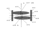
また次に図4は、本発明のSAW共振子に関するさらに他の一実施例について図1のIDT部位102の1対の電極指に限定して図示した電極パターン図である。反射器等の構成は幅方向Yの形状を図2と同一として図1のSAW共振子の構成をとる。図4を見ればわかる通り、連続的にかわる線幅 L(Y)の場合を図示したものである。図中の各部位の名称は、401と402は給電導体、403と404はIDTの電極指等である。405は弾性表面波の位相伝播方向であるX軸、406は前記X軸に直交して403,404等の中心軸(408,409)に平行に位置するY軸である。403,404等の電極指群は幅方向Yに関して、中心軸Xに関して対称関数からなる線幅L(Y)をもつ。407は電極指の中心軸(408,409)間の長さを示し、電極指の周期長Ptを表す。また図4の例は、幅方向Yの中央線幅が広く両側が細い例であるが、逆に中央部位が細く両側が広い場合もあることは容易に考えられる。
【0023】
次に本発明の実施例である図1、図2の特性につき前述の理論計算結果である図5、図6、図7、図8を用いて、実測結果である図9、図10の関係を説明する。
【0024】
まず、図5から説明する。図5は従来の一様な線幅 L(Y)=cnst.をもつSAW共振子において実現する固有モードの変位V(Y)を図示したものである。上から順に501がS0モード、A0(502)モード、S1(503)モード、A1モード(504)、S2(505)モードである。前記固有モードの周波数は、従来の構成であれば前記のS0、A0…の順に増加する。つぎに図6は前記線幅L(Y)が特定の条件を取る場合について、規格化ポテンシャル関数N(Y)の形(611,612,613)と、横モードの変位V(Y)(601,612,613)と、IDTにおける電極指(612,622,623)を図示したものである。
【0025】
まず、601,611,612で表わされる場合は、線幅L(Y)が中央部において細く、両側において広い場合である。この場合の前記関数N(Y)は、前記L(Y)が小さければ自由表面であるN(Y)=0に近く、L(Y)が大きければN(Y)は大きくなる。601の変位V(Y)は、N(Y)の大きな領域により多くの振動エネルギが蓄積されるため端部において振幅が増大する形となる。つぎに中央に配置した602,612,622の条件では、電極指622の線幅L(Y)=一定であり、幅方向変位V(Y)(602)は一様に端部に向かって減少する。またつぎに、変位603,N(Y)が613,623の電極指の条件の場合には、線幅L(Y)は中央部において広く両端部において細い場合である。この条件下では、幅方向変位V(Y)は、前述の602の場合より一層中央部に集中していることがわかる。変位601の例が図2の実施例に相当し、変位603の例が図1の実施例に相当する。変位602の例は従来の構成条件である。
【0026】
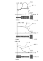
つぎに図7は前述の図5の各横モードが、図6の611で示されるN(Y)の状態を取った場合に示す共振周波数変化である。図6のY軸は5λ分割の目盛りがとられているから、線幅L(Y)が細い領域WCcは、40λの電極指交差幅WCの1/3であり、広い部分は片側40λの1/3である。図7の横軸は前記線幅L(Y)が細い領域のポテンシャルN(Y)が0.6から1.0の範囲で変化した場合である。縦軸は周波数変化率Δf/fを10-6(ppm)単位で表示した。図中の700はS0モードでこれがSAW共振子の主共振の直列共振周波数frに相当する。701はA0モード、702はSAW共振子の反共振周波数faである。703はS1モード、704はA1モード、705はS2モードである。図7から分かるとおりN=0.85にある点PにおいてS0モードとA0モードは交差しており、0.6から0.85の範囲あるいは線幅の関係としてLC/LS=0.6から0.85でにおいては、A0モード周波数f(A0)はS0モード周波数f(S0)より小さくなることがわかる。
【0027】
つぎに図8について説明する。図8は前述の図5の各横モードが、図6の611で示されるN(Y)の状態を取った場合に示す共振周波数変化である。Y軸は5λ分割の目盛りがとられているから、線幅L(Y)が細い領域は、40λの電極指交差幅WCの1/3であり、広い部分は片側40λの1/3である。図8の横軸は前記線幅L(Y)が広い領域のポテンシャルN(Y)が1.0から1.2の範囲あるいは線幅の関係としてLC/LS=1.0から1.2で変化した場合である。縦軸は周波数変化率Δf/fを10-6(ppm)単位で表示した。図中の800はS0モードでこれがSAW共振子の主共振の直列共振周波数frに相当する。801はA0モード、804はSAW共振子の反共振周波数faである。802はS1モード、803はA1モードである。図8から分かるとおり1.04付近にある点Qにおいて804の反共振周波数faとA0モードの周波数f(A0)は交差していることがわかる。
【0028】
つぎに、図7のP点と図8のQ点で製作したSAW共振子の共振特性を図9と図10に示す。図9は図8のQ点に対応するものであり、図10は図7のP点に対応している。
【0029】
まず図9から説明すると、900がS0モードの共振周波数fr(903)であり、901はA0モードの共振である。また、902はS1モードの共振である。904はS0モードの反共振周波数faである。901のA0モードは、反共振周波数faより十分にはなれた約1300ppm上に存在していることがわかる。従って、903のfrと904のfa間には、スプリアスとなる共振が存在しないため、良好な変動のない発振周波数が維持できる。ちなみに本発明のSAW共振子を用いて発振回路を構成した場合の発振周波数について図11を用いて解説する。図11中の1100の破線で囲まれた中はSAW共振子の等価回路であり、等価直列インダクタンスL1、等価直列キャパシタンスC1、等価直列抵抗R1、並列容量C0からなっている。1101で表される破線内は発振回路の増幅側の部分であって、CLは負荷容量、−Rは増幅回路がつくる負性抵抗である。この場合において得られる発振周波数foscは、次式となる。
【0030】
【数7】
![]()
【0031】
つぎに図10は、1000がS0モードの共振周波数fr(1003)であり、1001はA0モードの共振である。また、1002はS1モードの共振である。1004はS0モードの反共振周波数faである。1001のA0モードは、共振振周波数frより下側に約200ppmはなれたて存在していることがわかる。従って、1003のfrと1004のfa間には、スプリアスとなる共振が存在しないため、良好な変動のない発振周波数が維持できる。この関係は、図7のP点以下の規格化ポテンシャル値N(0.85以下0.6の範囲)であれば成り立つことが容易にわかる。
【0032】
以上、本発明のSAW共振子の構成および特性につき説明した。構成例は水晶STカットで示したが、他のカットである16度回転Y板であるLSTカットとか、9.6度回転Y板であるKカットでもよく、さらにまた水晶以外の圧電気材料であっても適合できることをつけくわえる。
【0033】
【発明の効果】
以上述べたように本発明によれば、例えば水晶基板を用いてSAW共振子の小型化をはかるに際して、前記SAW共振子のIDTを構成する電極指の線幅L(Y)に幅方向Yに対して変化する形状とすることにより、幅方向に対する振動エネルギの閉じ込め状態を変化させることにより所望の特性を得たものである。例えば、中央部の線幅LCを両側の線幅LSの関係をLC>LSとすれば、従来品よりエネルギ閉じ込め状態が良好なSAW共振子が得られ、逆に LC<LSとすれば、A0モードスプリアスを直列共振周波数より低下させることができ、スプリアスによって周波数変動が起きないSAW発振器が構成できる。その結果として、小型で良好な水晶SAW発振器を高速通信装置市場に提供でき、今後多大の利点が期待できる。
【図面の簡単な説明】
【図1】 本発明のSAW共振子の一実施例が有する導体パターンを示す平面図。
【図2】 本発明の他のSAW共振子の一実施例が示すIDTの導体パターン図。
【図3】 本発明の他のSAW共振子のIDTの一実施例が示す導体パターン図。
【図4】 本発明のさらに他のSAW共振子のIDTの一実施例が示す導体パターン図。
【図5】 本発明のSAW共振子が有する固有振動モード図。
【図6】 本発明の図1と図2が示す固有振動モード図。
【図7】 本発明の図2が示す特性図。
【図8】 本発明の図1が示す特性図。
【図9】 本発明の図1が示す共振特性図。
【図10】 本発明の図2が示す共振特性図。
【図11】 SAW発振回路の等価回路図。
【図12】 従来のSAW共振子が示す幅方向振動変位図。
【符号の説明】
100 圧電体平板
101 反射器1
102 IDT
103 反射器2
104 導体ストリップ
105,106 電極指[0001]
BACKGROUND OF THE INVENTION
The present invention relates to a SAW resonator that provides a technique useful for reducing the element size in a SAW resonator configured using surface acoustic waves.
[0002]
[Prior art]
As a conventional SAW resonator, there is one interdigital electrode (hereinafter abbreviated as IDT (Interdigital Transduser)) that applies an electrical alternating voltage to convert it into a surface acoustic wave, and a pair of reflectors on both sides thereof. A SAW resonator having a configuration consisting of the following is generally used (Japanese Patent Laid-Open No. 3-261210). The operating principle of the SAW resonator will be described in detail in the detailed description of the present invention. However, the so-called energy confined SAW resonator (reference document: energy confined surface acoustic wave resonator, scientific technique US87-36, pp9-). 16 (1987. 9)), and also in the propagation direction of the surface acoustic wave and the width direction perpendicular thereto, the confinement state of the vibration energy is good and the resonance sharpness (Q value) is relatively high. It has been widely used for SAW oscillators using VHF and UHF band frequencies.
[0003]
When a SAW resonator is configured with a quartz ST-cut X propagation substrate, which is a rotating Y plate of about 30 to 45 degrees with excellent frequency temperature characteristics using this configuration, the planar size of the element is (x × y) = A device having a characteristic of a series equivalent resistance R1 of about 20Ω at 200 MHz at 2 mm × 2.8 mm is obtained.
[0004]
[Problems to be solved by the invention]
However, for consumer devices that have recently been remarkably demanded for miniaturization and low cost, the SAW resonator with the frequency of about 200 MHz is the same as the conventional R1 performance at an element size of 1 mm x 2.8 mm, which is less than half the width of the conventional one. It was difficult to manufacture while maintaining the standard. When this cause is investigated, the main cause is that the number of wavelengths n in the width direction is reduced to about half with respect to the wavelength λ of the surface acoustic wave that depends on the frequency, and the energy confinement in the width direction in the SAW resonator is reduced. Is insufficient (see FIG. 12), and energy dissipation occurs at the width end of the element, resulting in a decrease in the Q value, resulting in an increase in R1. In FIG. 12, 1200 indicates the vibration displacement V (Y) in the width direction Y of the SAW resonator, 1201 indicates the electrode conductor pattern, 1202 indicates the end displacement ε of the vibration displacement, and 1203 indicates the outer shape of the element chip of the SAW resonator. Piezoelectric plate).
Accordingly, the present invention solves such problems, and its purpose is to reduce the size by using a substrate having excellent frequency temperature characteristics, such as quartz ST cut, and having an excellent material Q value. The purpose of the present invention is to provide a SAW resonator that is a scale and has a high Q value of the SAW resonator and, as a result, excellent frequency stability and good C / N.
[0005]
[Means for Solving the Problems]
(1) The SAW resonator of the present invention includes at least one interdigital electrode and a pair of reflectors for reflecting the surface acoustic wave generated by the interdigital electrode on both sides of the piezoelectric plate. The surface acoustic wave is disposed in the propagation direction (longitudinal direction X), and the reflector and the interdigital electrode are formed by periodically disposing metal parallel conductors on the piezoelectric plate, and the reflector and the interdigital transducer The distance between the adjacent parallel conductors between the interdigital electrodes consists of the space LT of the line LT and the space ST which one period length of the interdigital electrodes has, and the arrangement period length PT of the parallel conductors of the interdigital electrodes is defined as: In the SAW resonator which is a frequency rising energy confining type in which the total reflection coefficient Γ of the entire interdigital electrode is set to 10>Γ> 0.8, which is smaller than the arrangement period length PR of the reflector. Elasticity table With respect to the width direction Y perpendicular to the propagation direction X of the surface wave, the X-direction width dimension L (Y) of the parallel conductors constituting the reflector and the interdigital electrode is narrow at the center position in the width direction Y (dimension LC). And it is characterized by taking a wide dimension LS on both sides.
(2) In the above (1), the dimension L (Y) is given by a step-like function that changes symmetrically with respect to the center position in the width direction Y, and the reflector and the interdigital electrode each take n as an integer. (3) In the above (2), the dimension L (Y) has a relationship of Lc <Ls, and 3 (n) (n> 2). It is composed of parallel conductors having a line width.
(4) In the above (3), the dimension L (Y) follows the relational expression of Lc <Ls, and the fundamental wave oblique symmetry mode A0 has the fundamental wave symmetry mode S0 which is the transverse mode of the SAW resonator. The resonance frequency is small (f (S0)> f (A0)).
(5) In the above (4), the relational expression between the dimensions LC and LS is in the range of LC / LS = 0.6 to 0.85, and the portion having LC with respect to the full length WC of the electrode finger crossing width of the interdigital electrode The ratio of the length WCc is WCc / WC = 1/3.
(6) In the above (1), the piezoelectric flat plate is a crystal, is an ST cut of a 30-45 degree rotated Y plate, and the interdigital finger width WC is the wavelength of the surface acoustic wave. Λ is a range of 10λ to 40λ.
(7) In the above (1), the sum M + N of the interdigital number M of the interdigital electrodes and the number of conductors N of the one-side reflectors in the one SAW resonator is in the range of 150 to 200.
[0006]
DETAILED DESCRIPTION OF THE INVENTION
Before describing specific embodiments of the present invention, a theoretical explanation will be given to help understand the present invention.
A flat plate is cut out from a piezoelectric material such as quartz, lithium tantalate, PZT, lithium tetraborate, etc., and its surface is mirror-polished, and then the phase propagation direction of surface acoustic waves such as Rayleigh, SH, leaky, and BGS waves An IDT (interdigital electrode) in which a plurality of parallel conductor electrode fingers made of, for example, metal aluminum is periodically arranged is formed, and a pair of reflectors are provided on both sides of the IDT. Are arranged in parallel and periodically to form a 1-port SAW resonator.
[0007]
In the SAW resonator, when the IDT is constructed, the total reflection coefficient Γ of the entire electrode finger of the IDT is expressed by the following formula (1) when the positive electrode and the negative electrode are M pairs. Then, if 10>Г> 0.8, so-called energy-confined SAW resonator in which vibration energy is concentrated at the center of the resonator (reference: energy confined surface acoustic wave resonator, signal) It is known that the academic technique US87-36, pp9-16 (1987. 9)) can be realized.
[0008]
[Expression 1]
![]()
[0009]
For example, if the IDT is an ST cut quartz plate made of the aluminum conductor, b = 0.255, H / λ = 0.03, M = 80 pairs, and the number of conductors of one reflector is N = 100. With this configuration, a conventional 1-port SAW resonator can be configured. At this time, Γ = 2.448. When this configuration condition is applied to a frequency of 200 MHz, the surface acoustic wave velocity Vs of the ST cut is 3150 m / s, so that λ = 3150/200 = 15.75 μm / s, and the total length of the SAW resonator is Λ (M + N) = 2835 μm, which explains the validity of the total element size of 2.8 mm.
[0010]
In addition, when the WC is 40 wavelengths at the 200 MHz frequency, when the element width size y is 2 mm, R1 is about 20Ω, and when y = 1 mm, R1 varies in the range of 30 to 60Ω. . The present invention was obtained in the process of elucidating the cause and studying measures for obtaining a conventional R1 value. As a method of analysis, the following theoretical method was used.
[0011]
This is a design of a SAW resonator by calculating a vibration displacement and a resonance frequency of a so-called transverse mode in the width direction Y of the SAW resonator, and the contents will be described in order. The transverse mode is a natural vibration mode that exists depending on the length in the width direction of the SAW resonator (the Y-axis direction orthogonal to the propagation direction X of the surface acoustic wave). The length generally refers to the electrode finger crossing width WC of the IDT. The electrode finger crossing width WC is a dimension in the width direction in which the positive and negative electrode fingers overlap each other.
[0012]
Next, as a method for easily calculating the vibration displacement of the SAW resonator in the width direction (Y axis) of the SAW resonator, the inventors have already derived differential equations governing these transverse modes. (Takagi, Momozaki, et al .: “K-cut quartz SAW resonator with dynamic and static zero temperature coefficient at room temperature”, The Institute of Electrical Engineers of Japan, 25th EM Symposium, pp 79-80 (1996)). When this equation is described again, equation (2) is obtained.
[0013]
[Expression 2]
[0014]
[Equation 3]
[0015]
[Expression 4]
![]()
[0016]
[Equation 5]
[0017]
[Formula 6]
[0018]
Example 1
Hereinafter, embodiments of the present invention will be described in order from FIG. FIG. 1 is a plan view showing an electrode pattern used for one type of SAW resonator according to the present invention. In FIG. 1, the names of the respective parts are as follows: 100 is a piezoelectric plate, 102 is the entire interdigital electrode of the SAW resonator, and 101 and 103 are the
[0019]
Further supplementing the description, 100 piezoelectric flat plates are composed of a substrate having a piezoelectric single crystal such as quartz, lithium tantalate, and lithium tetraborate and a piezoelectric thin film such as ZnO. The IDT 102 and the
[0020]
(Example 2)
Next, FIG. 2 is an electrode pattern diagram illustrating another embodiment of the SAW resonator of the present invention limited to the IDT portion 102 of FIG. The configuration of the reflector and the like has the configuration of the SAW resonator of FIG. 1 with the same shape in the width direction Y as that of FIG. In the drawing, 201 and 202 are power supply conductors, 203 and 204 are IDT electrode fingers, and the like.
[0021]
(Example 3)
FIG. 3 is an electrode pattern diagram illustrating another embodiment of the SAW resonator according to the present invention limited to the IDT region 102 of FIG. The configuration of the reflector and the like is the same as the configuration of the SAW resonator in FIG. As can be seen from FIG. 3, n is an integer and n line widths Ln (n = 5) are illustrated. The name of each part in the figure is 301.
And 302 are power supply conductors, and 303 and 304 are IDT electrode fingers. 305 is an X axis which is a phase propagation direction of the surface acoustic wave, 306 is a Y axis which is perpendicular to the X axis and parallel to 303, 304, etc., and 307 is an electrode finger arrangement period length Pt. The electrode fingers such as 303 and 304 have different line widths Li (i = 1 to 5) in the five regions C1, C2, C3, C4, and C5 in the width direction Y. However, C1 and C5, C2 and C4 have the same line width. The example of FIG. 3 is an example in which the center line width in the width direction Y is wide and both sides are narrow, but conversely, the center part may be narrow and both sides may be wide.
[0022]
Example 4
FIG. 4 is an electrode pattern diagram showing still another embodiment relating to the SAW resonator of the present invention limited to a pair of electrode fingers at the IDT portion 102 of FIG. The configuration of the reflector and the like has the configuration of the SAW resonator of FIG. 1 with the same shape in the width direction Y as that of FIG. As can be seen from FIG. 4, the case of a line width L (Y) that changes continuously is illustrated. The names of the parts in the figure are 401 and 402 for power supply conductors, 403 and 404 for IDT electrode fingers, and the like.
[0023]
Next, the relationship between FIG. 9 and FIG. 10 which are actual measurement results using the above-mentioned theoretical calculation results of FIG. 5, FIG. 6, FIG. 7 and FIG. Will be explained.
[0024]
First, FIG. 5 will be described. FIG. 5 illustrates the natural mode displacement V (Y) realized in a conventional SAW resonator having a uniform line width L (Y) = cnst. In order from the top, reference numeral 501 denotes an S0 mode, an A0 (502) mode, an S1 (503) mode, an A1 mode (504), and an S2 (505) mode. The frequency of the eigenmode increases in the order of S0, A0,. Next, FIG. 6 shows the case where the line width L (Y) takes a specific condition, the form (611, 612, 613) of the normalized potential function N (Y), and the displacement V (Y) (601) of the transverse mode. 612, 613) and electrode fingers (612, 622, 623) in the IDT.
[0025]
First, the cases represented by 601, 611, and 612 are cases where the line width L (Y) is narrow at the center and wide at both sides. In this case, the function N (Y) is close to the free surface N (Y) = 0 if L (Y) is small, and N (Y) is large if L (Y) is large. The displacement V (Y) of 601 has a shape in which the amplitude increases at the end portion because more vibration energy is accumulated in a large region of N (Y). Next, under the conditions of 602, 612, and 622 arranged at the center, the line width L (Y) of the electrode finger 622 is constant, and the width direction displacement V (Y) (602) decreases uniformly toward the end. To do. Next, in the case of electrode finger conditions with displacements 603, N (Y) of 613, 623, the line width L (Y) is wide at the center and narrow at both ends. Under this condition, it can be seen that the width-direction displacement V (Y) is more concentrated in the center than in the case of 602 described above. An example of the
[0026]
Next, FIG. 7 shows a change in resonance frequency when each transverse mode in FIG. 5 takes the state of N (Y) indicated by 611 in FIG. Since the Y axis in FIG. 6 is graduated in 5λ divisions, the region WCc with a narrow line width L (Y) is 1/3 of the electrode finger crossing width WC of 40λ, and the wide portion is 1 on one side 40λ. / 3. The horizontal axis in FIG. 7 shows the case where the potential N (Y) in the region where the line width L (Y) is narrow changes in the range of 0.6 to 1.0. The vertical axis represents the frequency change rate Δf / f in units of 10 −6 (ppm). 700 in the figure is the S0 mode, which corresponds to the series resonance frequency fr of the main resonance of the SAW resonator.
[0027]
Next, FIG. 8 will be described. FIG. 8 shows the change in resonance frequency when each transverse mode in FIG. 5 takes the state of N (Y) indicated by 611 in FIG. Since the Y-axis is scaled in 5λ divisions, the region where the line width L (Y) is thin is 1/3 of the electrode finger crossing width WC of 40λ, and the wide portion is 1/3 of 40λ on one side. . The horizontal axis in FIG. 8 indicates that the potential N (Y) in the region where the line width L (Y) is wide is in the range of 1.0 to 1.2, or the relationship of L C / L S = 1.0 to 1. It is a case where it changes by 2. The vertical axis represents the frequency change rate Δf / f in units of 10 −6 (ppm). 800 in the figure is the S0 mode, which corresponds to the series resonance frequency fr of the main resonance of the SAW resonator. 801 is the A0 mode, and 804 is the anti-resonance frequency fa of the SAW resonator.
[0028]
Next, the resonance characteristics of the SAW resonator manufactured at point P in FIG. 7 and point Q in FIG. 8 are shown in FIGS. 9 corresponds to the point Q in FIG. 8, and FIG. 10 corresponds to the point P in FIG.
[0029]
First, referring to FIG. 9, 900 is the resonance frequency fr (903) of the S0 mode, and 901 is the resonance of the A0 mode.
[0030]
[Expression 7]
![]()
[0031]
Next, in FIG. 10, 1000 is the resonance frequency fr (1003) of the S0 mode, and 1001 is the resonance of the A0 mode.
[0032]
The configuration and characteristics of the SAW resonator of the present invention have been described above. The configuration example is shown with a quartz ST-cut, but other cuts such as an LST cut that is a 16-degree rotated Y plate or a K-cut that is a 9.6-degree rotated Y plate may be used. In addition, it can be adapted even if there is.
[0033]
【The invention's effect】
As described above, according to the present invention, for example, when a SAW resonator is miniaturized using a quartz substrate, the line width L (Y) of the electrode fingers constituting the IDT of the SAW resonator is set in the width direction Y. On the other hand, a desired characteristic is obtained by changing the confinement state of vibration energy in the width direction by adopting a shape that changes. For example, if the relationship between the line width L C at the center and the line width L S on both sides is L C > L S , a SAW resonator having a better energy confinement state than the conventional product can be obtained, and conversely L C <L If S , the A0 mode spurious can be lowered below the series resonance frequency, and a SAW oscillator can be configured in which no frequency fluctuation occurs due to the spurious. As a result, a small and good crystal SAW oscillator can be provided to the high-speed communication device market, and a great advantage can be expected in the future.
[Brief description of the drawings]
FIG. 1 is a plan view showing a conductor pattern included in an embodiment of a SAW resonator of the present invention.
FIG. 2 is a conductor pattern diagram of an IDT shown by an embodiment of another SAW resonator of the present invention.
FIG. 3 is a conductor pattern diagram showing an embodiment of an IDT of another SAW resonator according to the present invention.
FIG. 4 is a conductor pattern diagram showing an embodiment of an IDT of still another SAW resonator according to the present invention.
FIG. 5 is a natural mode diagram of the SAW resonator of the present invention.
6 is a natural vibration mode diagram shown in FIGS. 1 and 2 of the present invention. FIG.
FIG. 7 is a characteristic diagram shown in FIG. 2 of the present invention.
FIG. 8 is a characteristic diagram shown in FIG. 1 of the present invention.
FIG. 9 is a resonance characteristic diagram shown in FIG. 1 of the present invention.
FIG. 10 is a resonance characteristic diagram shown in FIG. 2 of the present invention.
FIG. 11 is an equivalent circuit diagram of a SAW oscillation circuit.
FIG. 12 is a vibration displacement diagram in the width direction shown by a conventional SAW resonator.
[Explanation of symbols]
100 Piezoelectric plate 101
102 IDT
103
104
Claims (7)
前記弾性表面波の伝搬方向Xに直交する幅方向Yに関して、前記反射器とすだれ状電極を構成する平行導体のX方向幅寸法L(Y)が、幅方向Yの中央位置において細く(寸法LC)、かつ両側において広い寸法Lsをとることを特徴とするSAW共振子。On the piezoelectric plate, at least one interdigital electrode and a pair of reflectors for reflecting the surface acoustic wave generated by the interdigital electrode on both sides thereof are provided with a propagation direction of the surface acoustic wave (longitudinal direction X The reflector and the interdigital electrode are formed by periodically arranging metal parallel conductors on the piezoelectric plate, and between the nearest parallel conductors between the reflector and the interdigital electrode. Is a space ST of the line LT and the space ST that one period length of the interdigital electrode has, and the arrangement period length PT of the parallel conductors of the interdigital electrode is set smaller than the arrangement period length PR of the reflector. In a SAW resonator that is a frequency rising energy confining type in which the total reflection coefficient Γ of the entire interdigital electrode is 10>Γ> 0.8,
With respect to the width direction Y orthogonal to the propagation direction X of the surface acoustic wave, the X-direction width dimension L (Y) of the parallel conductors constituting the reflector and the interdigital electrode is narrow at the center position in the width direction Y (dimension LC And a wide dimension Ls on both sides.
Priority Applications (1)
| Application Number | Priority Date | Filing Date | Title |
|---|---|---|---|
| JP2000073086A JP3864665B2 (en) | 2000-03-15 | 2000-03-15 | SAW resonator |
Applications Claiming Priority (1)
| Application Number | Priority Date | Filing Date | Title |
|---|---|---|---|
| JP2000073086A JP3864665B2 (en) | 2000-03-15 | 2000-03-15 | SAW resonator |
Publications (3)
| Publication Number | Publication Date |
|---|---|
| JP2001267880A JP2001267880A (en) | 2001-09-28 |
| JP2001267880A5 JP2001267880A5 (en) | 2005-03-03 |
| JP3864665B2 true JP3864665B2 (en) | 2007-01-10 |
Family
ID=18591392
Family Applications (1)
| Application Number | Title | Priority Date | Filing Date |
|---|---|---|---|
| JP2000073086A Expired - Fee Related JP3864665B2 (en) | 2000-03-15 | 2000-03-15 | SAW resonator |
Country Status (1)
| Country | Link |
|---|---|
| JP (1) | JP3864665B2 (en) |
Families Citing this family (10)
| Publication number | Priority date | Publication date | Assignee | Title |
|---|---|---|---|---|
| JP4671820B2 (en) * | 2005-09-09 | 2011-04-20 | 京セラ株式会社 | Surface acoustic wave device |
| JP2008035220A (en) * | 2006-07-28 | 2008-02-14 | Kyocera Corp | Surface acoustic wave device and communication equipment |
| DE102010005596B4 (en) * | 2010-01-25 | 2015-11-05 | Epcos Ag | Electroacoustic transducer with reduced losses due to transversal emission and improved performance by suppression of transverse modes |
| US8803402B2 (en) | 2010-03-04 | 2014-08-12 | Panasonic Corporation | Elastic wave device |
| JP5697751B2 (en) * | 2011-03-25 | 2015-04-08 | スカイワークス・パナソニック フィルターソリューションズ ジャパン株式会社 | Elastic wave device with high-order transverse mode wave suppressed |
| WO2014192756A1 (en) * | 2013-05-29 | 2014-12-04 | 株式会社村田製作所 | Acoustic wave device |
| WO2015007319A1 (en) * | 2013-07-18 | 2015-01-22 | Epcos Ag | Electroacoustic transducer with improved suppression of unwanted modes |
| JP6573836B2 (en) | 2016-01-13 | 2019-09-11 | 太陽誘電株式会社 | Elastic wave resonator, filter, and duplexer |
| WO2018079574A1 (en) * | 2016-10-28 | 2018-05-03 | 京セラ株式会社 | Acoustic wave element |
| CN110114973B (en) * | 2016-12-26 | 2024-04-26 | 株式会社村田制作所 | Elastic wave device |
-
2000
- 2000-03-15 JP JP2000073086A patent/JP3864665B2/en not_active Expired - Fee Related
Also Published As
| Publication number | Publication date |
|---|---|
| JP2001267880A (en) | 2001-09-28 |
Similar Documents
| Publication | Publication Date | Title |
|---|---|---|
| JP5488825B2 (en) | Surface acoustic wave resonator and surface acoustic wave oscillator | |
| EP2224591B1 (en) | Surface acoustic wave resonator and surface acoustic wave oscillator | |
| JP5934464B2 (en) | Surface acoustic wave resonator, surface acoustic wave oscillator, and electronic device | |
| JP5648908B2 (en) | Vibration device, oscillator, and electronic device | |
| JP2012060422A (en) | Surface acoustic wave device, electronic apparatus and sensor device | |
| JP2012060418A (en) | Surface acoustic wave device, electronic apparatus and sensor device | |
| US6774536B2 (en) | Surface acoustic wave device | |
| JP3864665B2 (en) | SAW resonator | |
| JP4059152B2 (en) | Surface acoustic wave resonator | |
| JPH09298446A (en) | Surface acoustic wave device and its design method | |
| JPS632414A (en) | Elastic surface wave resonator | |
| JP4059147B2 (en) | Surface acoustic wave resonator | |
| JP5563378B2 (en) | Elastic wave element | |
| JP3379383B2 (en) | Surface acoustic wave device | |
| US20110037343A1 (en) | Elastic Wave Device | |
| US8471434B2 (en) | Surface acoustic wave device, surface acoustic wave oscillator, and electronic apparatus | |
| JP6288760B2 (en) | Surface acoustic wave device, resonator and oscillation circuit | |
| KR102561687B1 (en) | Transducer structure for source suppression in SAW filter devices | |
| JP2003174351A (en) | Surface acoustic wave device and communication equipment | |
| JP2002111431A (en) | Elastic surface wave apparatus | |
| JP4868124B2 (en) | Surface acoustic wave resonator | |
| JP5750683B2 (en) | Two-terminal-pair surface acoustic wave resonator, surface acoustic wave oscillator and electronic device | |
| JP5737490B2 (en) | Transversal surface acoustic wave device, surface acoustic wave oscillator and electronic equipment | |
| JP3498729B2 (en) | Surface acoustic wave resonator | |
| JP2015084534A (en) | Two-terminal pair surface acoustic wave resonator, surface acoustic wave oscillator, and electronic apparatus |
Legal Events
| Date | Code | Title | Description |
|---|---|---|---|
| A521 | Written amendment |
Free format text: JAPANESE INTERMEDIATE CODE: A523 Effective date: 20040329 |
|
| A621 | Written request for application examination |
Free format text: JAPANESE INTERMEDIATE CODE: A621 Effective date: 20040329 |
|
| A977 | Report on retrieval |
Free format text: JAPANESE INTERMEDIATE CODE: A971007 Effective date: 20051205 |
|
| A131 | Notification of reasons for refusal |
Free format text: JAPANESE INTERMEDIATE CODE: A131 Effective date: 20060314 |
|
| A521 | Written amendment |
Free format text: JAPANESE INTERMEDIATE CODE: A523 Effective date: 20060427 |
|
| TRDD | Decision of grant or rejection written | ||
| A01 | Written decision to grant a patent or to grant a registration (utility model) |
Free format text: JAPANESE INTERMEDIATE CODE: A01 Effective date: 20060912 |
|
| A61 | First payment of annual fees (during grant procedure) |
Free format text: JAPANESE INTERMEDIATE CODE: A61 Effective date: 20060925 |
|
| R150 | Certificate of patent or registration of utility model |
Free format text: JAPANESE INTERMEDIATE CODE: R150 |
|
| FPAY | Renewal fee payment (event date is renewal date of database) |
Free format text: PAYMENT UNTIL: 20101013 Year of fee payment: 4 |
|
| FPAY | Renewal fee payment (event date is renewal date of database) |
Free format text: PAYMENT UNTIL: 20101013 Year of fee payment: 4 |
|
| FPAY | Renewal fee payment (event date is renewal date of database) |
Free format text: PAYMENT UNTIL: 20111013 Year of fee payment: 5 |
|
| FPAY | Renewal fee payment (event date is renewal date of database) |
Free format text: PAYMENT UNTIL: 20121013 Year of fee payment: 6 |
|
| FPAY | Renewal fee payment (event date is renewal date of database) |
Free format text: PAYMENT UNTIL: 20121013 Year of fee payment: 6 |
|
| FPAY | Renewal fee payment (event date is renewal date of database) |
Free format text: PAYMENT UNTIL: 20131013 Year of fee payment: 7 |
|
| S531 | Written request for registration of change of domicile |
Free format text: JAPANESE INTERMEDIATE CODE: R313531 |
|
| R350 | Written notification of registration of transfer |
Free format text: JAPANESE INTERMEDIATE CODE: R350 |
|
| LAPS | Cancellation because of no payment of annual fees |