JP3861356B2 - Oscillator circuit - Google Patents
Oscillator circuit Download PDFInfo
- Publication number
- JP3861356B2 JP3861356B2 JP05499697A JP5499697A JP3861356B2 JP 3861356 B2 JP3861356 B2 JP 3861356B2 JP 05499697 A JP05499697 A JP 05499697A JP 5499697 A JP5499697 A JP 5499697A JP 3861356 B2 JP3861356 B2 JP 3861356B2
- Authority
- JP
- Japan
- Prior art keywords
- circuit
- impedance
- negative
- oscillation
- oscillation circuit
- Prior art date
- Legal status (The legal status is an assumption and is not a legal conclusion. Google has not performed a legal analysis and makes no representation as to the accuracy of the status listed.)
- Expired - Fee Related
Links
Images


Landscapes
- Inductance-Capacitance Distribution Constants And Capacitance-Resistance Oscillators (AREA)
Description
【0001】
【発明の属する技術分野】
本発明は、例えばラジオ受信機、テレビジョン受信機、衛星放送受信機、ビデオレコーダー、移動体通信機等に用いられる制御型発振器に使用して好適な発振回路に関するものである。
【0002】
【従来の技術】
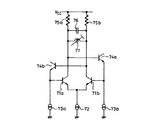
例えばテレビジョン受信機に用いられる制御型の発振回路においては、従来から例えば図7に示すような制御型発振回路が使用されている。すなわち図7は、従来の制御型発振回路の構成を示す。
【0003】
この図7において、トランジスタ71a、71bからなる差動対が設けられ、これらのトランジスタ71a、71bのエミッタが互いに接続されて、この接続中点が電流源72を通じて接地される。またトランジスタ71a、71bのベースがそれぞれ電流源73a、73bを通じて接地される。
【0004】
さらにトランジスタ71a、71bのコレクタが、それぞれエミッタホロアのトランジスタ74a、74bを通じて互いにもう一方のトランジスタ71a、71bのベースに接続される。そしてトランジスタ71a、71bのコレクタがそれぞれ抵抗75a、75bを通じて電源VCCに接続されると共に、これらのコレクタ間にキャパシタンス76とインダクタンス77の並列回路が接続される。
【0005】
従ってこの回路において、キャパシタンス76の値をC、インダクタンス77の値をLとすると、つぎの〔数1〕に示す共振周波数で発振が行われる。
【数1】

【発明が解決しようとする課題】
ところで上述の図7に示す制御型発振回路においては、その発振周波数はキャパシタンス76の値Cとインダクタンス77の値Lによって決定される。ところがこの場合に、インダクタンス77となるコイルは、いわゆるIC(集積回路)内には形成することができない。
【0007】
そこでこのようなコイルはICに外付けされることになるが、このようなコイルをICに外付けした場合には、まず外付けされたコイルからの輻射の問題が生じる。従ってこのような輻射の問題を解決するためには、いわゆるシールドケース等の輻射を遮断する手段を設けなくてはならず、部品コストや設置スペースの増大等の問題が新たに発生することになる。
【0008】
また、発振周波数の調整を行う場合には、上述の回路では外付けのコイル=インダクタンス77の値Lを可変することになるが、このようなコイルの値を可変するためには極めて高い熟練度が必要とされ、その結果として製造コストの上昇を招くことになる。さらに発振周波数の自動調整を考えた場合には、上述の回路でコイルの値の変更は、例えば直流での制御には不適当である。
【0009】
この出願はこのような点に鑑みて成されたものであって、解決しようとする問題点は、従来の制御型発振回路では、コイルをICに外付けするために輻射が発生し、部品コストや設置スペースの増大等の問題が生じると共に、外付けのコイル=インダクタンスの値の調整が困難で、さらに自動調整には不適当であるというものである。
【0010】
【課題を解決するための手段】
このため本発明においては、差動対のエミッタ間に接続されたインピーダンスを、電圧−電流変換回路を通してコレクタ間に電流帰還することにより負のインピーダンス回路を形成し、この負のインピーダンス回路を用いて発振回路を形成するようにしたものであって、これによれば、発振を行うインダクタンスをコイルを用いずに形成することができる。
【0011】
【発明の実施の形態】
以下、本発明について説明するに、まず最初に本発明の発振回路の前提となる負性インピーダンス発生回路について説明する。そこで図3は、前提となる負性インピーダンス発生回路の一例の構成を示す接続図である。
【0012】
この図3において、トランジスタ1a、1bからなる差動対が設けられる。そしてこれらのトランジスタ1a、1bのエミッタ間に、抵抗値R1 の抵抗21a、21bと、容量値C1 /2のコンデンサ22とが対称に設けられたインピーダンスが直列に接続されると共に、これらのエミッタがそれぞれ電流源3a、3bを通じて接地される。
【0013】
また、それぞれ電圧値±V1 の入力信号源4a、4bが、それぞれバッファ回路10を構成するトランジスタ5a、5bのベース−エミッタ間を通じてトランジスタ1a、1bのベースに接続される。また、トランジスタ5a、5bのエミッタがそれぞれ電流源6a、6bを通じて接地される。さらにトランジスタ1a、1bのコレクタが、互いにもう一方のトランジスタ1a、1bのベースに、それぞれトランジスタ5a、5bのベース−エミッタ間を通じて接続される。
【0014】
従ってこの回路において、トランジスタ1a、1bの各ベースには、入力信号源4a、4bからの電圧値±V1 の入力信号がそれぞれトランジスタ5a、5bのバッファ回路10を通じて印加される。そしてこれらの印加電圧±V1 が電流i1 に変換されるように電圧−電流変換回路20が構成されている。なおバッファ回路10は、直流シフト、及びトランジスタ1a、1bのベース方向の入力インピーダンスを上げる役割を兼ねているものである。
【0015】
そこでこの回路において、例えば電圧値+V1 の入力信号源4aから見た入力インピーダンスZ1 は、次の〔数2〕の式で表わされる。
【数2】
従ってこの図3の回路において、等価的に電圧値+V1 の入力信号に対して値−R1 と−C1 が直列に存在していることになる。ここでこの値−R1 、−C1 を並列インピーダンスZP の形で表現すると、この並列インピーダンスZP は、次の〔数3〕の式で表わされる。
【数3】
従ってこの回路において、抵抗21a、21bの値−R1 と、コンデンサ22の値−C1 /2を用いてインダクタンスを形成することができるものである。
【0018】
そこでさらに図4は、図3の負性インピーダンス回路を応用して負性キャパシタンス発生回路を形成した場合の一例の構成を示す。なお以下の説明で、上述の図3の回路と対応する部分には、同一符号を付して重複の説明を省略する。
【0019】
この図4において、負性キャパシタンス発生回路は、上述の図3のトランジスタ1a、1bのコレクタに、それぞれ抵抗値R2 の抵抗23a、23bを対称に接続したものでる。
【0020】
この場合に、キャパシタンス22に流れる電流の値をi1 として、例えば電圧値+V1 の入力信号源4aから見た入力インピーダンスZC は、次の〔数4〕の式で表わされる。
【数4】
そしてこの図4の回路において、R1 =R2 とした場合には、
ZC =−1/SC1
となって、入力インピーダンスZC は負のキャパシタンスのみとなり、負性キャパシタンス発生回路を形成することができる。
【0022】
そこでこの負性キャパシタンス発生回路を、上述のコイルに代えてインダクタンスとして用いることにより、発振回路を形成することができる。
【0023】
すなわち本発明においては、差動対を有し、差動対のエミッタ間にインピーダンスを接続して電圧−電流変換用コンダクタンスを形成し、差動対のコレクタ出力を互いにもう一方のベース入力へ帰還してエミッタ間に接続されたコンダクタンスを負性のインピーダンスとしてコレクタ負荷へ電流帰還することにより、差動対のコレクタ側から見た入力インピーダンスとして負性のインピーダンスを発生する負性インピーダンス発生回路を形成すると共に、差動対のコレクタ間に対称に抵抗とコンデンサによる1次のローパスフィルタを形成するコレクタ負荷を接続し、負性インピーダンス発生回路及びコレクタ負荷による開ループの伝達関数が2次のフィルタ特性を有し、且つその分母の1次の項がマイナスとなる値に各インピーダンスの係数比を定めることにより、コレクタ負荷に帰還される負性のインピーダンスをインダクタンスとして扱うようにしたことを特徴とするものである。
【0024】
以下、図面を参照して本発明を説明するに、図1は本発明による発振回路の一例の構成を示す接続図である。すなわち図1は、図4の負性キャパシタンス発生回路を用いて発振回路を形成した場合の一例の構成を示す。なお以下の説明で、上述の図3、図4の回路と対応する部分には、同一符号を付して重複の説明を省略する。
【0025】
この図1において、本発明の発振回路は、上述の図4の負性キャパシタンス発生回路の差動対を構成するトランジスタ1a、1bのコレクタに接続される抵抗23a、23bの他端を直接に電源VCCに接続すると共に、これらのコレクタ間に容量値C2 /2のキャパシタンス7を接続したものである。またこれらのコレクタから、出力電圧値±VO を取り出す出力端子8a、8bが導出される。
【0026】
さらに図2は、説明のために上述の図1の回路のループを切り、抵抗23a、23bの他端間に入力電圧値±VINの信号源9a、9bを設けた開ループの形で表したものである。
【0027】
そこでこの図2において、入力VIN、出力VO の伝達関数T[S] は、次の〔数5〕の式で表わされる。
【数5】
この〔数5〕に示す伝達関数T[S] において、分母の第2項(2φS)に注目すると、この第2項がマイナスの場合(∴φ<0)に、回路が発振することを示している。すなわちこのことは、〔数5〕に示した伝達関数T[S] を逆ラプラス変換することによって明らかになる。
【0029】
そこで次の〔数6〕は、〔数5〕に示した伝達関数T[S] を逆ラプラス変換した結果の関数VO(t)を示す。
【数6】
ここでこれらの〔数5〕及び〔数6〕において、上述の回路の発振条件は、φ<0、θ2 >0である。
【0031】
そこでφ<0を〔数5〕の式から求めると、次の〔数7〕の式となる。
【数7】
そしてこれらの条件式において、φ<0、C1,C2,R1,R2 は全て正の数であることを考慮すると、次の〔数8〕の式となる。
【数8】
一方、上述の発振条件のθ2 >0について考えると、〔数5〕の式において、ωO 2 =1/C1 C2 R1 R2 、φ=ωO /Qとおくと、〔数5〕の式の分母は次の〔数9〕の式のように表される。
【数9】
そしてこの条件式において、θ2 >0の条件を満たすのは次の〔数10〕の式となる。
【数10】
従って、上述の回路を構成する素子の値C1,C2,R1,R2 及びQが、以上〔数7〕〔数8〕〔数10〕の式を満たすとき、〔数5〕で表した伝達関数T[S] において、分母の1次の項がマイナスとなり、回路が発振するものである。
【0036】
こうしてこの回路において、差動対のエミッタ間に接続されたインピーダンスを、電圧−電流変換回路を通してコレクタ間に電流帰還することにより負のインピーダンス回路を形成し、この負のインピーダンス回路を用いて発振回路を形成するようにしたものであって、これによれば、発振を行うインダクタンスをコイルを用いずに形成することができる。
【0037】
これによって、従来、シリコンを用いたIC(集積回路)では困難とされていた純度の高い発振回路がIC内に作り出せ、高価な外付け部品を必要としなくなる。また、キャリアーの純度があがるため各種検波器に使用した場合、S/N等の性能向上となる。また、発振回路が完全にIC内に取り込まれるため、外部への副射等の問題がなくなる。これらの理由により結果として商品の性能向上、製造コストの削減、基板面積縮小などの利点をもたらすものである。
【0038】
さらに図5及び図6は、本発明の発振回路の応用として、可変周波数発振回路を形成する場合の構成を示す。すなわちこれらの回路においては、上述の負性インピーダンス発生回路と、コレクタ負荷に関連して可変インピーダンス回路を設けて発振周波数を可変とするものである。
【0039】
まず図5の回路においては、負性インピーダンス発生回路とコレクタ負荷との間にバランス型の電流制御回路を設けて可変インピーダンス回路とする。
【0040】
すなわち図5において、負性インピーダンス発生回路を構成するトランジスタ1a、1bのコレクタと、コレクタ負荷(抵抗23a、23b、キャパシタンス7)との間にトランジスタ31a、31b、32a、32bからなるバランス型の電流制御回路30を設ける。そしてこれらのトランジスタ31aと32a、31bと32bのベース間に、制御電圧VC の電圧源33が接続される。
【0041】
従ってこの回路において、制御電圧VC を変化させることによって、回路を流れる信号電流i1 にある係数kを掛けてi2 (=ki1 )に変換させることができる。そしてこの変換によって、コレクタ負荷に付く負性インピーダンスを変化させることができる。
【0042】
そこで、出力電圧VO から見た負性インピーダンスZC は次の〔数11〕の式で表される。
【数11】
従って、この場合の伝達関数TC[S]=VO /VINは、次の〔数12〕の式で表わされる。
【数12】
そしてこの回路において、制御電圧VC を変化させることによって、係数kが変化され、この変化によって発振周波数が変化されるものである。なお、このとき係数kの取り得る範囲は、φ<0、C1,C2,R1,R2 は全て正の数であることを考慮すると、次の〔数13〕の式で表わされる。
【数13】
さらに図6の回路においては、上述のコレクタ負荷(キャパシタンス7)に並列に可変インピーダンス回路を設けるものである。
【0046】
すなわち図6において、負性インピーダンス発生回路を構成するトランジスタ1a、1bのコレクタがそれぞれ抵抗値R3 の抵抗41a、41bを通じてトランジスタ42a、42bのベースとコレクタに接続される。またこれらのトランジスタ42a、42bのエミッタが互いに接続される。そしてこの接続中点が制御電流IC の電流源43を通じて接地される。
【0047】
従ってこの回路において、制御電流IC を変化させることによって、例えば電流IC を大きくするとトランジスタ42a、42bのエミッタ抵抗値が減少し、抵抗値R3 の抵抗41a、41bがキャパシタンス7に並列に付加された値に近付くことになる。これによって可変インピーダンス回路40が形成され、コレクタ負荷に付く負性インピーダンスを変化させることができる。
【0048】
そこで、出力電圧VO から見た負性インピーダンスZD は次の〔数14〕の式で表される。
【数14】
従って、この場合の伝達関数TD[S]=VO /VINは、次の〔数15〕の式で表わされる。
【数15】
そしてこの回路において、制御電流IC を変化させることによって、可変インピーダンス回路40の抵抗値は値R3 から∞まで変化され、この変化によって発振周波数が変化されるものである。
【0051】
なお、このとき抵抗値R3 の取り得る範囲を考えると、条件として上述の〔数15〕で表される伝達関数TD[S]の分母の1次の項がマイナスであることから、C1 R1 +C2 R2 −C1 R2 (1−R1 /R3 )<0である。ここで値C1,C2,R1,R2 は全て正の実数であることから、明らかに0<(1−R1 /R3 )であることが必要条件である。さらにこれを書き換えるとR3 >R1 である。
【0052】
従って抵抗値R3 がR1 <R3 <∞の範囲で変化されされたとき、(1−R1 /R3 )は、0<(1−R1 /R3 )<1の値を取る。よって上述のC1 R1 +C2 R2 −C1 R2 (1−R1 /R3 )<0の条件より、R3 >R1 /(1−R1 /R2 −C2 /C1 )でなくてはいけないことになる。
【0053】
すなわち、R1 <R3 <∞の条件を満たすためには、1>(R1 /R2 −C2 /C1 )>0を満たすことが、C1,C2,R1,R2 の条件であることがわかる。以上をまとめて次の〔数16〕に示す。
【数16】
こうしてこの回路において、上述の負性インピーダンス発生回路と、コレクタ負荷に関連して可変インピーダンス回路を設けることにより、発振周波数を可変とすることができるものである。
【0055】
これによって、従来、シリコンを用いたIC(集積回路)では困難とされていた純度の高い発振回路の発振周波数を電圧コントロールすることが可能となるため、その応用範囲が広がり、PLL回路や、AM復調器、FM復調器、及び周波数コンバートシステム等の幅広い用途への利用が可能であるなど、数多くの利点をもたらすものである。
【0056】
【発明の効果】
以上詳述した本発明によれば、差動対のエミッタ間に接続されたインピーダンスを、電圧−電流変換回路を通してコレクタ間に電流帰還することにより負のインピーダンス回路を形成し、この負のインピーダンス回路を用いて発振回路を形成するようにしたものであって、これによれば、発振を行うインダクタンスをコイルを用いずに形成することができる。
【0057】
これによって、従来、シリコンを用いたIC(集積回路)では困難とされていた純度の高い発振回路がIC内に作り出せ、高価な外付け部品を必要としなくなる。また、キャリアーの純度があがるため各種検波器に使用した場合、S/N等の性能向上となる。また、発振回路が完全にIC内に取り込まれるため、外部への副射等の問題がなくなる。これらの理由により結果として商品の性能向上、製造コストの削減、基板面積縮小などの利点をもたらすものである。
【0058】
また本発明によれば、従来、シリコンを用いたIC(集積回路)では困難とされていた純度の高い発振回路の発振周波数を電圧コントロールすることが可能となるため、その応用範囲が広がり、PLL回路や、AM復調器、FM復調器、及び周波数コンバートシステム等の幅広い用途への利用が可能であるなど、数多くの利点をもたらすものである。
【図面の簡単な説明】
【図1】本発明の適用される発振回路の一例の構成図である。
【図2】その説明のための回路図である。
【図3】本発明の説明のための負性インピーダンス発生回路の一例の構成図である。
【図4】本発明の説明のための負性キャパシタンス発生回路の一例の構成図である。
【図5】本発明の適用される制御型発振回路の一例の構成図である。
【図6】本発明の適用される制御型発振回路の他の例の構成図である。
【図7】従来の制御型発振回路の構成図である。
【符号の説明】
1a,1b 差動対を構成するトランジスタ、21a,21b 抵抗、22 キャパシタンス、23a,23b 抵抗、3a,3b 電流源、5a,5b バッファ回路を構成するトランジスタ、6a,6b 電流源、7 キャパシタンス、8a,8b 出力端子、VCC 電源、20 電圧−電流変換回路[0001]
BACKGROUND OF THE INVENTION
The present invention relates to an oscillation circuit suitable for use in a controlled oscillator used in, for example, a radio receiver, a television receiver, a satellite broadcast receiver, a video recorder, a mobile communication device, and the like.
[0002]
[Prior art]
For example, in a control type oscillation circuit used in a television receiver, for example, a control type oscillation circuit as shown in FIG. 7 is conventionally used. That is, FIG. 7 shows a configuration of a conventional control type oscillation circuit.
[0003]
In FIG. 7, a differential pair composed of
[0004]
Further, the collectors of the
[0005]
Therefore, in this circuit, when the value of the
[Expression 1]
[Problems to be solved by the invention]
Incidentally, in the control type oscillation circuit shown in FIG. 7, the oscillation frequency is determined by the value C of the
[0007]
Therefore, such a coil is externally attached to the IC. However, when such a coil is externally attached to the IC, there is a problem of radiation from the externally attached coil. Therefore, in order to solve such a radiation problem, it is necessary to provide a means for blocking radiation such as a so-called shield case, and new problems such as an increase in parts cost and installation space will occur. .
[0008]
When adjusting the oscillation frequency, the above-described circuit changes the value L of the external coil =
[0009]
This application has been made in view of the above points, and the problem to be solved is that in the conventional control type oscillation circuit, radiation is generated to externally attach the coil to the IC, and the component cost is reduced. In addition, there are problems such as an increase in installation space and the like, and it is difficult to adjust the value of the external coil = inductance, which is inappropriate for automatic adjustment.
[0010]
[Means for Solving the Problems]
For this reason, in the present invention, a negative impedance circuit is formed by feeding back the impedance connected between the emitters of the differential pair between the collectors through the voltage-current conversion circuit, and using this negative impedance circuit. An oscillation circuit is formed, and according to this, an inductance for oscillating can be formed without using a coil.
[0011]
DETAILED DESCRIPTION OF THE INVENTION
Hereinafter, the present invention will be described. First, a negative impedance generation circuit which is a premise of the oscillation circuit of the present invention will be described. Therefore, FIG. 3 is a connection diagram showing a configuration of an example of a negative impedance generating circuit as a premise.
[0012]
In FIG. 3, a differential pair composed of
[0013]
The
[0014]
Accordingly, in this circuit, the input signals of the voltage value ± V 1 from the
[0015]
Therefore, in this circuit, for example, the input impedance Z 1 seen by the input signal source 4a of the voltage value + V 1 is represented by the formula for [Equation 2].
[Expression 2]
Therefore, in the circuit of FIG. 3, the values −R 1 and −C 1 exist equivalently in series with respect to the input signal having the voltage value + V 1 . Wherein the value -R 1, when representing a -C 1 in the form of a parallel impedance Z P, the parallel impedance Z P is represented by the formula for a Formula 3.
[Equation 3]
Therefore, in this circuit, an inductance can be formed by using the value -R 1 of the
[0018]
Therefore, FIG. 4 further shows an example of a configuration in which a negative capacitance generation circuit is formed by applying the negative impedance circuit of FIG. In the following description, parts corresponding to those in the circuit of FIG. 3 described above are denoted by the same reference numerals, and redundant description is omitted.
[0019]
In FIG. 4, negative capacitance generating circuit, the
[0020]
In this case, assuming that the value of the current flowing through the
[Expression 4]
In the circuit of FIG. 4, when R 1 = R 2 ,
Z C = -1 / SC 1
Thus, the input impedance Z C is only negative capacitance, and a negative capacitance generation circuit can be formed.
[0022]
Therefore, an oscillation circuit can be formed by using this negative capacitance generation circuit as an inductance instead of the above-described coil.
[0023]
That is, in the present invention, a differential pair is provided, an impedance is connected between the emitters of the differential pair to form a voltage-current conversion conductance, and the collector outputs of the differential pair are fed back to the other base input. Then, a negative impedance generation circuit that generates a negative impedance as an input impedance viewed from the collector side of the differential pair is formed by feeding back the conductance connected between the emitters as a negative impedance to the collector load. In addition, a collector load that forms a first-order low-pass filter with a resistor and a capacitor is connected symmetrically between the collectors of the differential pair, and the open-loop transfer function by the negative impedance generation circuit and the collector load has a second-order filter characteristic. And the relationship of each impedance to a value in which the first-order term of the denominator is negative. By determining the ratio, it is characterized in that a negative impedance is fed back to the collector load was treated as an inductance.
[0024]
Hereinafter, the present invention will be described with reference to the drawings. FIG. 1 is a connection diagram showing a configuration of an example of an oscillation circuit according to the present invention. That is, FIG. 1 shows an example of a configuration in which an oscillation circuit is formed using the negative capacitance generation circuit of FIG. In the following description, portions corresponding to the circuits in FIGS. 3 and 4 described above are denoted by the same reference numerals, and redundant description is omitted.
[0025]
1, the oscillation circuit of the present invention directly supplies the other ends of
[0026]
Further, FIG. 2 is shown in the form of an open loop in which the circuit of FIG. 1 described above is cut for explanation, and
[0027]
Therefore, in FIG. 2, the transfer function T [S] of the input V IN and the output V O is expressed by the following equation (5).
[Equation 5]
In the transfer function T [S] shown in [ Equation 5], when attention is paid to the second term (2φS) of the denominator, it indicates that the circuit oscillates when the second term is negative (∴φ <0). ing. That is, this becomes clear by inverse Laplace transform of the transfer function T [S] shown in [Equation 5].
[0029]
Therefore, the following [Equation 6] shows a function V O (t) as a result of inverse Laplace transform of the transfer function T [S] shown in [Equation 5].
[Formula 6]
Here, in these [Equation 5] and [Equation 6], the oscillation conditions of the circuit described above are φ <0 and θ 2 > 0.
[0031]
Therefore, if φ <0 is obtained from the formula [5], the following formula 7 is obtained.
[Expression 7]
In these conditional expressions, considering that φ <0 and C 1 , C 2 , R 1 , R 2 are all positive numbers, the following expression (8) is obtained.
[Equation 8]
On the other hand, when θ 2 > 0 in the above-described oscillation condition is considered, in the formula [5], when ω O 2 = 1 / C 1 C 2 R 1 R 2 and φ = ω O / Q, The denominator of the equation [5] is expressed as the following equation [9].
[Equation 9]
In this conditional expression, the following expression (10) satisfies the condition of θ 2 > 0.
[Expression 10]
Therefore, when the values C 1 , C 2 , R 1 , R 2 and Q of the elements constituting the above circuit satisfy the formulas [Equation 7] [Equation 8] [Equation 10], In the transfer function T [S] shown , the first-order term of the denominator becomes negative, and the circuit oscillates.
[0036]
Thus, in this circuit, a negative impedance circuit is formed by feeding back the impedance connected between the emitters of the differential pair between the collectors through the voltage-current conversion circuit, and an oscillation circuit is formed using this negative impedance circuit. According to this, the inductance for oscillating can be formed without using a coil.
[0037]
As a result, a high-purity oscillation circuit, which has conventionally been difficult with an IC (integrated circuit) using silicon, can be produced in the IC, and expensive external parts are not required. In addition, since the purity of the carrier is increased, performance such as S / N is improved when used for various detectors. In addition, since the oscillation circuit is completely taken into the IC, problems such as external secondary emission are eliminated. For these reasons, as a result, advantages such as improved product performance, reduced manufacturing costs, and reduced substrate area are brought about.
[0038]
Further, FIGS. 5 and 6 show a configuration in the case of forming a variable frequency oscillation circuit as an application of the oscillation circuit of the present invention. That is, in these circuits, the above-described negative impedance generation circuit and a variable impedance circuit are provided in association with the collector load to make the oscillation frequency variable.
[0039]
First, in the circuit of FIG. 5, a balanced current control circuit is provided between the negative impedance generation circuit and the collector load to form a variable impedance circuit.
[0040]
That is, in FIG. 5, a balanced current consisting of
[0041]
Therefore, in this circuit, by changing the control voltage V C , the signal current i 1 flowing through the circuit can be multiplied by a certain coefficient k to be converted into i 2 (= ki 1 ). By this conversion, the negative impedance applied to the collector load can be changed.
[0042]
Therefore, the negative impedance Z C viewed from the output voltage V O is expressed by the following equation (11).
[Expression 11]
Accordingly, the transfer function T C [S] = V O / V IN in this case is expressed by the following equation (Equation 12).
[Expression 12]
In this circuit, the coefficient k is changed by changing the control voltage V C, and the oscillation frequency is changed by this change. At this time, the possible range of the coefficient k is expressed by the following equation (13) considering that φ <0 and C 1 , C 2 , R 1 and R 2 are all positive numbers. .
[Formula 13]
Furthermore, in the circuit of FIG. 6, a variable impedance circuit is provided in parallel with the collector load (capacitance 7) described above.
[0046]
That is, in FIG. 6, the
[0047]
Therefore, in this circuit, for example, when the current I C is increased by changing the control current I C , the emitter resistance values of the
[0048]
Therefore, the negative impedance Z D viewed from the output voltage V O is expressed by the following equation (14).
[Expression 14]
Accordingly, the transfer function T D [S] = V O / V IN in this case is expressed by the following equation (15).
[Expression 15]
And in this circuit, by changing the control current I C, the resistance value of the
[0051]
Considering the possible range of the resistance value R 3 at this time, since the first-order term of the denominator of the transfer function T D [S] expressed by the above [Formula 15] is negative as a condition, C 1 R 1 + C 2 R 2 -C 1 R 2 (1-
[0052]
Therefore, when the resistance value R 3 is changed in the range of R 1 <R 3 <∞, (1-R 1 / R 3 ) takes a value of 0 <(1-R 1 / R 3 ) <1. . Therefore, R 3 > R 1 / (1-R 1 / R 2 -C 2 / C from the above-mentioned condition of C 1 R 1 + C 2 R 2 -C 1 R 2 (1-R 1 / R 3 ) <0. 1 ) It must be.
[0053]
That is, in order to satisfy the condition of R 1 <R 3 <∞, satisfying 1> (R 1 / R 2 −C 2 / C 1 )> 0 satisfies C 1, C 2, R 1, R 2. It turns out that it is the conditions of. The above is summarized in the following [Equation 16].
[Expression 16]
Thus, in this circuit, the oscillation frequency can be made variable by providing the above-described negative impedance generation circuit and the variable impedance circuit in relation to the collector load.
[0055]
As a result, it is possible to control the oscillation frequency of a high-purity oscillation circuit, which has heretofore been difficult with an IC (integrated circuit) using silicon, so that the application range is expanded, and a PLL circuit, AM It offers many advantages such as being usable in a wide range of applications such as a demodulator, FM demodulator, and frequency conversion system.
[0056]
【The invention's effect】
According to the present invention described in detail above, the negative impedance circuit is formed by feeding back the impedance connected between the emitters of the differential pair between the collectors through the voltage-current conversion circuit. Thus, an oscillation circuit is formed using this, and according to this, an inductance for oscillating can be formed without using a coil.
[0057]
As a result, a high-purity oscillation circuit, which has conventionally been difficult with an IC (integrated circuit) using silicon, can be produced in the IC, and expensive external parts are not required. In addition, since the purity of the carrier is increased, performance such as S / N is improved when used for various detectors. In addition, since the oscillation circuit is completely taken into the IC, problems such as external secondary emission are eliminated. For these reasons, as a result, advantages such as improved product performance, reduced manufacturing costs, and reduced substrate area are brought about.
[0058]
Further, according to the present invention, it is possible to control the voltage of the oscillation frequency of a high-purity oscillation circuit, which has conventionally been difficult with an IC (integrated circuit) using silicon. It provides many advantages such as being usable in a wide range of applications such as circuits, AM demodulator, FM demodulator, and frequency conversion system.
[Brief description of the drawings]
FIG. 1 is a configuration diagram of an example of an oscillation circuit to which the present invention is applied.
FIG. 2 is a circuit diagram for explanation.
FIG. 3 is a configuration diagram of an example of a negative impedance generation circuit for explaining the present invention.
FIG. 4 is a configuration diagram of an example of a negative capacitance generation circuit for explaining the present invention.
FIG. 5 is a configuration diagram of an example of a controlled oscillation circuit to which the present invention is applied.
FIG. 6 is a configuration diagram of another example of a control type oscillation circuit to which the present invention is applied.
FIG. 7 is a configuration diagram of a conventional controlled oscillation circuit.
[Explanation of symbols]
1a, 1b Transistors constituting a differential pair, 21a, 21b resistors, 22 capacitances, 23a, 23b resistors, 3a, 3b current sources, 5a, 5b Transistors constituting buffer circuits, 6a, 6b Current sources, 7 capacitances, 8a , 8b Output terminal, V CC power supply, 20 Voltage-current conversion circuit
Claims (5)
上記差動対のエミッタ間にインピーダンスを接続して電圧−電流変換用コンダクタンスを形成し、
上記差動対のコレクタ出力を互いにもう一方のベース入力へ帰還して上記エミッタ間に接続されたコンダクタンスを負性のインピーダンスとしてコレクタ負荷へ電流帰還することにより、
上記差動対のコレクタ側から見た入力インピーダンスとして負性のインピーダンスを発生する負性インピーダンス発生回路を形成すると共に、
上記差動対のコレクタ間に対称に抵抗とコンデンサによる1次のローパスフィルタを形成するコレクタ負荷を接続し、
上記負性インピーダンス発生回路及びコレクタ負荷による開ループの伝達関数が2次のフィルタ特性を有し、且つその分母の1次の項がマイナスとなる値に各インピーダンスの係数比を定めることにより、
上記コレクタ負荷に帰還される上記負性のインピーダンスをインダクタンスとして扱うようにした
ことを特徴とする発振回路。Having a differential pair,
An impedance is connected between the emitters of the differential pair to form a conductance for voltage-current conversion,
By feeding back the collector output of the differential pair to the other base input and feeding back the current connected to the collector load as a negative impedance of the conductance connected between the emitters,
While forming a negative impedance generation circuit that generates a negative impedance as an input impedance viewed from the collector side of the differential pair,
A collector load that forms a first-order low-pass filter with a resistor and a capacitor is connected symmetrically between the collectors of the differential pair,
By determining the coefficient ratio of each impedance to a value in which the open loop transfer function by the negative impedance generation circuit and the collector load has a second-order filter characteristic and the first-order term of the denominator is negative,
An oscillation circuit characterized in that the negative impedance fed back to the collector load is treated as an inductance .
上記負性インピーダンス発生回路を負性キャパシタンス発生回路とする
ことを特徴とする発振回路。The oscillation circuit according to claim 1,
An oscillation circuit, wherein the negative impedance generation circuit is a negative capacitance generation circuit.
上記コレクタ負荷に関連して可変インピーダンス回路を設けて発振周波数を可変とした
ことを特徴とする発振回路。The oscillation circuit according to claim 1,
Oscillating circuit, characterized in that it has a variable oscillation frequency in relation to the upper Symbol collector load providing a variable impedance circuit.
上記負性インピーダンス発生回路とコレクタ負荷との間にバランス型の電流制御回路を設けて上記可変インピーダンス回路とした
ことを特徴とする発振回路。The oscillation circuit according to claim 3, wherein
An oscillation circuit characterized in that a balanced current control circuit is provided between the negative impedance generation circuit and a collector load to form the variable impedance circuit.
上記コレクタ負荷に並列に上記可変インピーダンス回路を設ける
ことを特徴とする発振回路。The oscillation circuit according to claim 3, wherein
An oscillation circuit comprising the variable impedance circuit in parallel with the collector load.
Priority Applications (1)
| Application Number | Priority Date | Filing Date | Title |
|---|---|---|---|
| JP05499697A JP3861356B2 (en) | 1997-03-10 | 1997-03-10 | Oscillator circuit |
Applications Claiming Priority (1)
| Application Number | Priority Date | Filing Date | Title |
|---|---|---|---|
| JP05499697A JP3861356B2 (en) | 1997-03-10 | 1997-03-10 | Oscillator circuit |
Publications (2)
| Publication Number | Publication Date |
|---|---|
| JPH10256830A JPH10256830A (en) | 1998-09-25 |
| JP3861356B2 true JP3861356B2 (en) | 2006-12-20 |
Family
ID=12986280
Family Applications (1)
| Application Number | Title | Priority Date | Filing Date |
|---|---|---|---|
| JP05499697A Expired - Fee Related JP3861356B2 (en) | 1997-03-10 | 1997-03-10 | Oscillator circuit |
Country Status (1)
| Country | Link |
|---|---|
| JP (1) | JP3861356B2 (en) |
Families Citing this family (5)
| Publication number | Priority date | Publication date | Assignee | Title |
|---|---|---|---|---|
| JP4945856B2 (en) * | 2001-05-28 | 2012-06-06 | ソニー株式会社 | Oscillator circuit |
| JP4713939B2 (en) | 2005-05-19 | 2011-06-29 | ルネサスエレクトロニクス株式会社 | Voltage controlled oscillator and wireless communication device using the same |
| FR2905042B1 (en) | 2006-08-17 | 2008-12-12 | St Microelectronics Sa | INTEGRATED ELECTRONIC CIRCUIT HAVING A TUNABLE RESONATOR |
| FR2905041A1 (en) | 2006-08-17 | 2008-02-22 | St Microelectronics Sa | Negative capacitance circuit for forming voltage controlled oscillator, has two branches connected between two reference potentials, and linearizing resistor parallely connected between two emitter electrodes of bipolar transistors |
| US8228120B2 (en) * | 2009-05-29 | 2012-07-24 | Intersil Americas Inc. | Negative capacitance synthesis for use with differential circuits |
-
1997
- 1997-03-10 JP JP05499697A patent/JP3861356B2/en not_active Expired - Fee Related
Also Published As
| Publication number | Publication date |
|---|---|
| JPH10256830A (en) | 1998-09-25 |
Similar Documents
| Publication | Publication Date | Title |
|---|---|---|
| CN1069463C (en) | Voltage controlled oscillator | |
| CN101904096A (en) | Variable inductor | |
| US6380816B1 (en) | Oscillator and voltage controlled oscillator | |
| US5192884A (en) | Active filter having reduced capacitor area but maintaining filter characteristics | |
| JP3921362B2 (en) | Temperature compensated crystal oscillator | |
| WO2002031961A1 (en) | Voltage controlled oscillator having a phase noise reduction device | |
| JP3861356B2 (en) | Oscillator circuit | |
| US6747499B2 (en) | Tunable quadrature phase shifter using an all-pass circuit | |
| US4990872A (en) | Variable reactance circuit producing negative to positive varying reactance | |
| AU2249597A (en) | Bridge-stabilized oscillator circuit and method | |
| KR940007972B1 (en) | Variable frequency oscillator | |
| JP2004526356A (en) | LC controllable oscillator, quadrature oscillator, and communication device | |
| KR19990008229A (en) | Frequency dependent resistors | |
| US5559479A (en) | Voltage control oscillator variable capacitance diode biasing circuit | |
| US7109814B2 (en) | Piezoelectric oscillator | |
| US20020158678A1 (en) | Tunable quadrature phase shifter | |
| US6124763A (en) | Oscillator with two outputs in quadrature | |
| US6683508B1 (en) | System and method of increasing a self-resonant frequency of a tuning circuit and an oscillator employing the same | |
| US5136254A (en) | FM demodulator circuit whose demodulation output is decreased in distortion | |
| JPH0563438A (en) | Voltage control oscillator | |
| JP3700338B2 (en) | 90 degree phase shifter | |
| JPH0319506A (en) | Crystal oscillation circuit | |
| JP2576193B2 (en) | Oscillation circuit | |
| EP0755115A1 (en) | Active low pass filter | |
| JPS6238323Y2 (en) |
Legal Events
| Date | Code | Title | Description |
|---|---|---|---|
| A977 | Report on retrieval |
Free format text: JAPANESE INTERMEDIATE CODE: A971007 Effective date: 20060113 |
|
| A131 | Notification of reasons for refusal |
Free format text: JAPANESE INTERMEDIATE CODE: A131 Effective date: 20060228 |
|
| A521 | Written amendment |
Free format text: JAPANESE INTERMEDIATE CODE: A523 Effective date: 20060403 |
|
| TRDD | Decision of grant or rejection written | ||
| A01 | Written decision to grant a patent or to grant a registration (utility model) |
Free format text: JAPANESE INTERMEDIATE CODE: A01 Effective date: 20060905 |
|
| A61 | First payment of annual fees (during grant procedure) |
Free format text: JAPANESE INTERMEDIATE CODE: A61 Effective date: 20060918 |
|
| LAPS | Cancellation because of no payment of annual fees |