JP3858523B2 - Objective lens - Google Patents
Objective lens Download PDFInfo
- Publication number
- JP3858523B2 JP3858523B2 JP21172599A JP21172599A JP3858523B2 JP 3858523 B2 JP3858523 B2 JP 3858523B2 JP 21172599 A JP21172599 A JP 21172599A JP 21172599 A JP21172599 A JP 21172599A JP 3858523 B2 JP3858523 B2 JP 3858523B2
- Authority
- JP
- Japan
- Prior art keywords
- region
- objective lens
- dvd
- light
- reproduction
- Prior art date
- Legal status (The legal status is an assumption and is not a legal conclusion. Google has not performed a legal analysis and makes no representation as to the accuracy of the status listed.)
- Expired - Lifetime
Links
Images


Classifications
-
- G—PHYSICS
- G11—INFORMATION STORAGE
- G11B—INFORMATION STORAGE BASED ON RELATIVE MOVEMENT BETWEEN RECORD CARRIER AND TRANSDUCER
- G11B7/00—Recording or reproducing by optical means, e.g. recording using a thermal beam of optical radiation by modifying optical properties or the physical structure, reproducing using an optical beam at lower power by sensing optical properties; Record carriers therefor
- G11B7/12—Heads, e.g. forming of the optical beam spot or modulation of the optical beam
- G11B7/135—Means for guiding the beam from the source to the record carrier or from the record carrier to the detector
- G11B7/1392—Means for controlling the beam wavefront, e.g. for correction of aberration
-
- G—PHYSICS
- G11—INFORMATION STORAGE
- G11B—INFORMATION STORAGE BASED ON RELATIVE MOVEMENT BETWEEN RECORD CARRIER AND TRANSDUCER
- G11B7/00—Recording or reproducing by optical means, e.g. recording using a thermal beam of optical radiation by modifying optical properties or the physical structure, reproducing using an optical beam at lower power by sensing optical properties; Record carriers therefor
- G11B7/12—Heads, e.g. forming of the optical beam spot or modulation of the optical beam
- G11B7/135—Means for guiding the beam from the source to the record carrier or from the record carrier to the detector
- G11B7/1372—Lenses
- G11B7/1374—Objective lenses
-
- G—PHYSICS
- G11—INFORMATION STORAGE
- G11B—INFORMATION STORAGE BASED ON RELATIVE MOVEMENT BETWEEN RECORD CARRIER AND TRANSDUCER
- G11B7/00—Recording or reproducing by optical means, e.g. recording using a thermal beam of optical radiation by modifying optical properties or the physical structure, reproducing using an optical beam at lower power by sensing optical properties; Record carriers therefor
- G11B2007/0003—Recording, reproducing or erasing systems characterised by the structure or type of the carrier
- G11B2007/0006—Recording, reproducing or erasing systems characterised by the structure or type of the carrier adapted for scanning different types of carrier, e.g. CD & DVD
Landscapes
- Physics & Mathematics (AREA)
- Optics & Photonics (AREA)
- Optical Head (AREA)
Description
【0001】
【発明の属する技術分野】
本発明は、対物レンズに係り、特に基板厚さの異なる光ディスクの互換再生に関する。
【0002】
【従来の技術】
近年、光ディスクは高密度化の一途をたどり、民生用再生専用光ディスクである0.65GBのCD−ROMに対して4.7GBのDVD−ROMが発売されている。ところがDVDとCDでは基板の厚さが異なり、DVDでは0.6mm、CDでは1.2mmである。このような違いは、記録密度の向上の目的で対物レンズの集光力の指標であるレンズの集光角度のsin値、すなわち開口数(NA)を、DVDでは、CDの0.45より大きい0.6としたため、ディスク傾きなどによる収差の発生を抑えたことによる。DVDドライブ装置においてはCDの再生が必須と考えられ、このようなディスク基板厚さの違いは対物レンズの対応基板厚の選択において問題となる。
【0003】
まずこの対応基板厚の意味について説明する。光ディスクでは通常、ほこりなどにより記録情報の再生ができなくなることを防ぐため、記録面をつけたポリカーボネートなどの透明基板の裏側から基板越しに記録膜面に光を集光して再生している。このようにすると例えば基板厚さ0.6mmのDVDの場合、基板の表面での光スポットは0.5mm程度になり、0.1mm以下程度の大きさのほこりであれば読み取りにあまり影響を及ぼさない。これにより光ディスクでは磁気ディスクと異なり、ユーザが自分でディスクを交換して再生することができている。ところがこのように基板越しに光を集光する場合、対物レンズはその基板厚さに合わせた形状とする必要がある。例えば理想的に集光されている光束中に、ある厚さを持った透明基板を挿入すると、基板に対して垂直に入射する光線と、斜めに入射する光線では、当然ながら後者の方が基板中の光路が長くなる。このような光路差が収差と呼ばれていて、光が絞れなくなる原因となる。ところがこのような収差は、あらかじめ挿入される基板の厚さがわかっていれば、レンズの形状によって補償することが可能である。したがって光ディスク装置の光ヘッドでは、通常再生する光ディスクの基板厚を特定して、それに対応した対物レンズを用いる。以上のように対応基板厚とは、ある対物レンズによる集光光束中に挿入して収差を生じることなく、光を理想的に集光できる基板の厚さである。
【0004】
このように通常の個々の光ディスク用対物レンズには対応基板厚が決まっているため、DVDとCDとの互換再生において問題となっていた。
【0005】
これに対して例えば特開平6−124477号では、液晶を用いてCD再生においては開口を制限して収差の大きい周辺部を遮光することにより、DVD用レンズによるCD再生における基板厚誤差による収差を低減していた。基板厚誤差によって生じる収差は球面収差と呼ばれ、NAの4乗に比例して増大する。したがって開口によりNAを小さくすると収差も低減する。一方、DVD再生では遮光しないように開口の有り無しをきりかえて用いる。ここで本従来例はDVD用の再生波長である650nmによりCDを再生することを意図している。つまり従来のCDに用いられていた波長780nmよりも波長が短かい。集光スポット径は波長をλとするとλ/NAに比例するため、波長が短いと必要なNAも小さくできる。したがって結果的にCD再生を650nmで行なうことで開口のNAを0.45より小さくでき、これによって従来例では必要な収差低減効果を得ていた。ところが従来例には、CDと互換性があり、最近普及の著しい書き込み可能なCD−R(CD−Recordable)の再生には対応できないという問題点がある。というのはCD−Rは記録膜に780nmでのみ十分な反射率を有する色素媒体を用いており、DVD再生波長650nmでは反射率が低下し、信号再生ができないからである。CD−Rを再生するには780nmの光源を別途、光ヘッドに搭載する必要がある。このとき波長は従来のCDと同じになるため制限開口のNAは従来の0.45以上にする必要があり、十分な収差の低減効果が得られなくなる。
【0006】
また他の従来例として特開平9−237431号では、輪帯状領域の光を遮蔽する方法が述べられている。ここではDVD用レンズでCDを再生するときに収差が大きく変化し始める輪帯領域の光を遮蔽することにより、CD再生の光スポットを直接劣化させる領域のみ除去する方法である。というのは収差が非常に大きく、波面の傾きが大きい領域の光線は波面の垂直方向に進行するため、焦点の位置から大きくはずれて散逸し、実質スポット性能に影響を及ぼさないからである。 DVD再生においては輪帯状の遮光領域より内側と外側の光は実質上収差なく集光される。このとき輪帯状遮蔽領域の光はDVD再生でも遮光されるが、その領域を許容範囲に狭くすることにより、液晶のような素子を用いることなく、実質上同等の効果を得ることができる。ところが逆に実質上開口を制限するのと等価であるため、これも780nmによるCD−R再生には対応できないという問題点がある。
【0007】
またさらに従来の他の技術が、特開平8−55363号に記載されている。ここでは基板厚さの異なる2種類の光ディスクを異なる波長の光源でそれぞれ再生し、2つの半導体レーザのレンズからの距離を変えることで対物レンズに入射する光の発散または収束の状態をずらし、これによって基板厚さずれによる球面収差を補償する方法が述べられている。この方法を用いればCD再生に780nm、DVD再生に650nmの半導体レーザを用いて、1つの対物レンズでDVDとCDの互換再生ができ、合わせてCD−Rの再生も可能である。ところがこのように2つの光源の位置を異ならせると、半導体レーザと対物レンズとの相対的な位置ずれの許容範囲が狭くなることが知られている。というのは対物レンズの設計において、入射光の入射角がずれてもコマ収差が急激に発生しない条件として正弦条件とよばれる条件が存在するが、これは特定の物像間距離でのみ成立し、2種類の物像間距離の両立は不可能であるからである。すなわち例えば波長650nmの半導体レーザの配置で正弦条件を満たすと、780nmの半導体レーザの配置ではこれを満たすことができない。この場合たとえばディスクが偏心して回転していると、トラッキング制御のときに対物レンズがそれに追随して移動することになり、半導体レーザとの相対位置がずれて急激に収差が発生してしまう。
【0008】
従来のさらに他の技術は、例えば本発明者らによる特開平10−255305号に記載されている。ここでは図1に示すように、対物レンズ1の対応基板厚が内側領域11で0.76mm、外側領域12で0.6mmのレンズに、輪帯溝状の凹部で形成された輪帯位相シフタ13が作られている。輪帯位相シフト領域の対応基板厚は内側領域と同じ0.76mmとなっている。ここではCDとDVDの対応基板厚の両立のため、レンズの光軸に近い中央部分の領域のみ対応基板厚を、DVDにおける0.6mmからややCDの1.2mmに近づけた0.76mmにしてCD再生において中心領域で発生する収差を低減し、さらに残留する収差を低減し、基板厚誤差でDVD再生において発生する収差をも低減するため、輪帯位相シフタ13を用いている。なお、この対物レンズは650nmの光も、780nmの光も平行光として対物レンズに入射させることを想定しており、上記の従来例にあるような対物レンズずれによってどちらかの波長の光が急激に増大することがないという利点がある。
【0009】
図2は従来例におけるDVD再生時とCD再生時の波面収差の計算値である。ここで波面収差とは光源である半導体レーザから、対物レンズまでの光路長の誤差をレンズの有効光束(瞳)における光線位置について表したものである。ただし図2においては収差が±0.5λを越える範囲は実質的に等しい位相値である±0.5λの範囲に折りたたんで表示している。輪帯位相シフタの位相シフト量はCD再生において−1.76λとしている。ここで負の位相シフトは光路長が短くなることを意味し、段差が凹であることを示す。するとCDでは実質、この小数点以下の位相シフト量が±0.5λの範囲となるように2を加算した0.24λの正の位相シフトが加わることになる。一方DVD再生では屈折率が波長780nmで1.583、650nmで1.586として、−1.76/(1.583−1)×780/650×(1.586−1)=−2.12λとなる。これについても位相シフト量が±0.5λの範囲となるように2を加算すると−0.12λとなり、図2に示すような負の位相シフトが加わることになる。このような効果はそれぞれの波長で要求される位相シフトの符号が決まっているため、輪帯位相シフタが凹の場合と凸の場合で等価でない。たとえば凸の位相シフタで上記とほぼ同等の位相シフト量を実現するためには、CDの位相シフト量を+3.24λとして、3.24/(1.583−1)×780/650×(1.586−1)=3.91λとなり位相シフト量が±0.5λの範囲となるように4を減算して−0.09λとなる。ところがこのように整数部を含めた位相シフトの絶対値が大きくなると、段差が深くなり加工が難しくなるばかりか、温度変動による波長ずれなどによる位相シフト量の誤差がほぼ整数部に比例して増大する。したがってここでは段差は凹とするのが望ましい。以上のようにして図2のように得られた波面収差については、マレシャルの基準によれば光スポットが良好に集光されるには、例えばRMS値が0.07λ(λは光波長)以下であることが必要である。これに対してDVD再生においてはRMS波面収差0.02λとなり良好な性能を有している。CD再生においては、波面収差が周辺部分で非常に大きくなっているものの、設計上有効なNAの範囲においては上記基準を満たしている。周辺部の収差の大きい光は波面の傾斜が非常に大きいため容易に散逸し、実質的に中心部分のみによる光スポットへの影響はない。このようにしてDVD、CD、CD−R再生において、互換再生が実現できた。
【0010】
【発明が解決しようとする課題】
輪帯位相シフタを対物レンズに一体成形する上記従来例においては、CD−Rの再生のみに対応し、CD−R記録装置では収差の低減が十分でないという問題点があった。というのはCD−R記録装置ではCDの記録情報ピットと同等の記録マークを高精度に記録するため、再生のNAより大きいNA0.5の対物レンズを用いているからである。上記従来例はCD−Rについても再生しか考慮していないため、波長780nmでNA0.45のCD−ROM光ピックアップと同等の光スポットしか形成できない。したがってNA0.5の範囲においては収差が増大して、CD−R記録に対応できない。
【0011】
上記問題点に鑑み、本発明において解決すべき課題は、DVD再生とCD−R記録を両立する対物レンズを実現することである。
【0012】
【課題を解決するための手段】
上記課題を解決するため、少なくとも2面の屈折面を有する上記従来例における対物レンズにおいて、2面の少なくとも一方に、レンズの光軸付近の円形領域が段差を持って突出させる。すなわち輪帯陥没領域である輪帯位相シフタとシフト方向が反転した円形突出領域である円形位相シフタを付加する。このようにすると図2における中心領域の波面収差の凹凸を軽減し、RMS波面収差を低減でき、CD再生における有効光束を拡張し、CD−R記録に必要な光スポット性能を実現できる。
【0013】
またこのとき、上記従来例において述べたように、少なくともこの円形突出領域は、最適基板厚をDVD基板厚0.6mmより、CD基板厚1.2mmに近い基板厚さとしておく。すなわちこの領域のみについて言えば、基板厚が0.6mmの光ディスクを再生する場合よりも、基板厚が0.6mmより厚い光ディスクを再生するときの方が収差が小さくなる。また同時に輪帯陥没領域より外側の領域においては、DVDに対して最適なように、対応基板厚を0.6mmとしておく。すなわち基板厚が0.6mmの光ディスクを再生するときが最も収差の小さい形状とする。
【0014】
さらに具体的には、全有効光束径に対する上記円形突出領域への入射光束径比をR1、前記輪帯陥没領域の内径にかかる光束径比をR2、前記輪帯陥没領域の外径にかかる光束径比をR3とするとき、
0.22≦R1≦0.35、0.40≦ R2≦0.50、0.75≦R3≦0.82、R1≦ R2≦ R3
を満たすようにすると効果がある。
【0015】
またこのような対物レンズにおいて少なくとも内側の円形突出領域におけるもっとも収差の小さくなる基板厚さが0.74mm以上0.85mm以下となるようにすると、より効果が大きい。
【0016】
またこのような対物レンズを、少なくとも2つの波長の半導体レーザ、およびレンズやプリズム、ミラー、光検出器などと一体として光ヘッドを構成することにより、初めてDVD再生とCD−R記録の両立が可能な光ヘッドとなる。
【0017】
さらにこのような2波長の光源を搭載した光ヘッドに用いる対物レンズにおいて、上記円形突出領域、および輪帯陥没領域における段差によって生じる光路長差がそれぞれφ1およびφ2、2つの波長のうち長い波長、すなわちCD再生波長をλ1とするとき、1.67λ1≦φ1≦1.87λ1、−1.87λ1≦φ2≦−1.67λ1
を満たすようにすると効果がある。
【0018】
このとき同時に2つの波長のうち短い波長、すなわちDVD再生波長をλ2とするとき、2.00λ2≦φ1≦2.24λ2、−2.24λ2≦φ2≦−2.00λ2を満たすようになる。
【0019】
またこれらの段差を有する対物レンズと、少なくとも2つの波長の半導体レーザ、およびレンズやプリズム、ミラー、光検出器などと一体として光ヘッドを構成することにより、初めてDVD再生とCD−R記録の両立が可能な光ヘッドとなる。
【0020】
またこのような光ヘッドを、少なくとも2種類の基板厚さの光ディスクをともに再生または記録再生できるような機構、および制御回路、などを一体として光ディスク装置を形成することにより初めてDVD再生とCD−R記録の両立が可能な光ディスク装置となる。
【0021】
【発明の実施の形態】
以下、図を用いて本発明の実施の形態を説明する。
【0022】
図3は本発明による対物レンズ3の概略形状を示す図である。ここでは図1に示した対物レンズと同様にして輪帯陥没領域である輪帯位相シフタ31を含む中心領域の最適基板厚をd1とし、それよりも外側の領域の最適基板厚をd2としている。d2についてはDVD、CD、CD−Rの互換再生のためには0.6mmとすればよい。DVD再生、およびCD再生におけるこの基板厚誤差による収差を、少ない位相シフトの絶対値でともに低減するため、輪帯陥没領域である輪帯位相シフタ31は前記従来例と同様、凹状の溝で構成されている。さらに本発明においては、輪帯陥没領域である輪帯位相シフタ31の内側に凸状の円形突出領域である円形位相シフタ32が付加されている。これによりCD再生、DVD再生における収差をさらに低減することをねらっている。
【0023】
図4はCD再生時における有効NAに対して、DVDでの再生波面収差許容値を変えて、前記従来例において述べた輪帯位相シフタを用いた方法と、今回の新しい形状における設計での規格化中心強度を示したグラフである。CDの再生波長は0.785μm、DVDの再生波長は0.655μm、DVD再生NAは0.6、基板厚はCD1.2mm、DVD0.6mmである。また最適化にあたっては円形突出領域と輪帯陥没領域での位相差の絶対値は等しく、円形突出領域では正(光路長増)、輪帯陥没領域では負の位相シフト(光路長減)を与え、最適基板厚の変化の境界は輪帯陥没領域の外径と一致させている。ここで規格化中心強度とは前記従来例、特開平10−255305において述べたように、有効NAの範囲内に入射する一様な強度の総光量に対して集光スポットの中心強度の比を示しており、いわゆるストレール強度に全NAに対する有効NAの比の2乗をかけたものである。ストレール強度はRMS波面収差をWrms、波長をλとするとき、1−(2πWrms/λ)2に相当し、収差の許容範囲の基準であるマレシャルの基準では、ストレール強度0.8以上、すなわちWrms ≒0.07λ以下が必要であると言われている。しかしながら収差がある場合に最適な制限開口のNAを決めるには、単なるストレール強度では評価指標としては適切でない。なぜならストレール強度はNAを固定したときの収差の評価基準であって、この場合のようにNAの異なる光スポットの良否は評価できないからである。NAが大きいほど、収差がない場合の光スポットは小さくなるので、ベースとなる光スポットは小さくなるが、収差はNAが大きいほど大きくなるのでスポットの劣化はより顕著になる。したがって収差とNAのバランスで最適なNAがあるはずであり、その評価指標としてここでは上記の規格化中心強度を用いている。たとえばNA0.6で無収差の規格化中心強度は1、無収差のCD−R記録用光スポットは、NA0.5で無収差であるからその規格化中心強度は(0.5/0.6)2=0.694である。CD−R記録用光スポットでマレシャル基準の収差がある場合にはこの0.8倍であり、0.556となる。したがって収差がある光スポットでは規格化中心強度が0.556以上である必要がある。図4においてはこの無収差のCD−R記録スポットのレベルを太い実線で、マレシャル基準を破線で示している。設計値の曲線は大きく2組あり、1組はピークにおいても破線を越えないのに対して、もう1組はNA0.48から0.53位の範囲において破線を越えている。前者が従来設計による値であり、後者が本発明による新しい設計法による計算結果である。それぞれ複数の曲線があるのは、DVD再生において許容するRMS収差の値を変えたものであり、それぞれ上から0.029λ、0.025λ、0.021λである。この程度の値はマレシャル基準に比べて十分小さく、設計上の残存収差としても許容できる。また当然ながらDVDの許容収差値が大きいほどCD再生スポットの品質が向上し、規格化中心強度が大きくなる。このように本発明においてはCD用光スポットの有効NAを約0.51にすれば、CD−R記録用光スポットのマレシャル基準を上まわる光スポットが実現できることがわかる。
【0024】
図5は図4の新しい形状の設計における、内側円形突出領域、輪帯陥没領域内径、輪帯陥没領域外径の設計値を示したものであり、縦軸はNA値で領域境界を示している。それぞれ図4におけるDVD再生での異なる許容収差値での設計値を重ねて表示している。これによれば領域境界位置はDVD再生での許容収差値にはほどんど依存していないことがわかる。マレシャル条件以上の範囲となるこれらの値は、内側円形突出領域はNA値で約0.14〜約0.20、輪帯陥没内側は約0.25〜約0.29、輪帯陥没外径は約0.45〜約0.49の範囲となっている。NA0.42以下で輪帯陥没内径と外径が一致しているのは、輪帯陥没領域が存在しない方が規格化中心強度が高いことを示しており、その場合の数値は有効NAと一致した値を表示している。
【0025】
図6は図4の本発明での設計における、輪帯陥没部の位相シフト量を示している。なお、すでに述べたように円形突出領域での位相シフト量は輪帯陥没領域と絶対値を等しく、符号を反転させている。これによれば位相シフト量はDVD再生時の許容収差量によって異なり、0.021λから0.029λの範囲においては、位相シフト量はCD再生波長0.785μmをλとして約−1.81〜約−1.74λの範囲でマレシャル条件を上回る。
【0026】
図7は図4の本発明での設計における、内側領域の最適基板厚を示している。ここですでに述べたように最適基板厚変化の境界は輪帯陥没領域の外径に一致させている。これによれば内側最適基板厚はDVD再生時の許容収差量によって異なり、0.021λから0.029λの範囲においては、約0.85〜0.74mmの範囲であることがわかる。DVDの許容収差が大きいほどCDに適した形状が許容されるため、内側最適基板厚は1.2mmに近づいている。またCD再生の有効NAが小さいほど、CD用の領域が狭くなるため、内側基板厚は1.2mmに近い値が許容される方向となっている。
【0027】
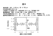
図8は図4におけるDVD波面収差許容値0.029λのときのおそらく最も規格化中心強度の高い結果を探索した設計例における波面収差形状である。このときCDの有効NAは0.509であった。図2に比べて段差部が増えているものの、CDにおける収差の低い領域が拡大していることがわかる。このとき内側最適基板厚は0.81mm、CDにおける位相シフト量は円形突出領域の位相シフタで1.781λ、輪帯陥没領域の位相シフタで−1.781λ、DVDにおける位相シフト量は円形突出領域の位相シフタで2.134λ、輪帯陥没領域の位相シフタで−2.134λである。これらは小数点以下が±0.5λ以下になるように整数部に2を加算または減算すると、円形突出領域の位相シフタで−0.219λ、輪帯陥没領域の位相シフタで0.219λ、DVDにおける位相シフト量は円形突出領域の位相シフタで0.134λ、輪帯陥没領域の位相シフタで−0.134λである。グラフでは実質的にこの値が位相シフトに作用している。また境界部のNAは円形突出領域の位相シフタ外縁部が0.182、輪帯陥没領域の位相シフタ内径部が0.275、輪帯陥没領域の位相シフタ外縁部が0.475、CD−R記録NAが0.509である。
【0028】
図9はDVDの波面収差を図8の実施例よりやや改善させることを意図し、図4でのDVD許容波面収差0.025λのときのCD再生での規格化中心強度の最大値を探索した結果得られた設計例における波面収差形状である。このとき内側最適基板厚は0.78mm、CDにおける位相シフト量は円形突出領域の位相シフタで1.78λ、輪帯陥没領域の位相シフタで−1.78λ、DVDにおける位相シフト量は円形突出領域の位相シフタで2.133λ、輪帯陥没領域の位相シフタで−2.133λである。これらは小数点以下が±0.5λ以下になるように整数部に2を加算または減算すると、円形突出領域の位相シフタで−0.22λ、輪帯陥没領域の位相シフタで0.22λ、DVDにおける位相シフト量は円形突出領域の位相シフタで0.133λ、輪帯陥没領域の位相シフタで−0.133λである。また境界部のNAは円形突出領域の位相シフタ外縁部が0.183、輪帯陥没領域の位相シフタ内径部が0.272、輪帯陥没領域の位相シフタ外縁部が0.475、CD−R記録NAが0.51である。
【0029】
図10にCD−R記録用の従来の光ヘッドにおけるディスク面上スポットプロファイルの計算結果を示す。ここで同じプロファイルに対して、左は鳥瞰図、右は等高線図である。なおここでは波長785nm、NA0.5、入射光のレンズエッジにおける強度(リム強度)は図中x側で0.76、y側で0.15として強度分布はガウス分布を仮定している。また等高線図の下の数値はスポット径とサイドローブ強度であり、WHXはx方向の半値全幅、WHYはy方向の半値全幅、WEXはx方向の1/e^2の全幅、WEYはy方向の1/e^2の全幅、SDXはx方向のサイドローブ強度の中心強度比、SDYはy方向のサイドローブ中心強度比である。スポット径の単位はすべてμmである。
【0030】
図11に、これに比較して例えば図8で示した波面収差形状を与える本発明による対物レンズのCD−R記録用スポットプロファイルを示す。ここでは集光のNAは0.6であり、収差の大きい周辺部分の光も合わせて計算している。リム強度は図10に対してNAの大きい分、低減している。これによればスポット径は若干増大しているものの、誤差は1%程度であってほとんどばらつきの範囲内であると考えられる。
【0031】
図12は同様にして、通常のDVD専用のレンズを用いて、波長655nmでDVDを再生するときの光スポットプロファイルの計算結果である。このとき対物レンズへの入射光の強度分布は、やはりガウス分布を仮定し、リム強度はx方向で0.57、y方向で0.49である。
【0032】
これに対して図13が図8に波面収差形状を示した本発明による対物レンズを用いて、波長655nmでDVDを再生するときの光スポットプロファイルの計算結果である。入射光の条件は図8と同一である。これについてはスポット径、サイドローブ強度ともほとんど図12と同等の光スポットが得られていることがわかる。
【0033】
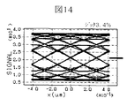
図14は図10に示した通常のCD−R用対物レンズによる光スポットを用いて、CD−ROMを再生した場合の再生信号アイパターンを計算したものである。これはCD−ROMのランダムなコードパターンについて、再生信号を再生クロックに同期させて重ねたもので、ちょうどオシロスコープにおいて再生信号の立ち上がりをトリガーとして同期をとって表示した信号に相当する。信号品質の評価指標は中央部の格子の交差部の幅であり、クロックとの時間方向のずれの標準偏差として表したジッタを格子の幅(検出窓幅)で規格化してパーセント表示した値を用いる。図14ではこの値が3.4%であった。ただし計算においては、隣接トラックのクロストーク、および最大反射光量に対して約1%のスライスレベルの変動を仮定している。通常、NA0.45のCD−ROM用光ヘッドの再生信号ジッタは理想状態で6〜7%程度と考えられ、CD−R記録対応によりNAが0.5に増大した効果が表れていることがわかる。
【0034】
図15は図14と同様の計算を、図11に示した本発明による対物レンズによる光スポットを用いて行なったものである。ジッタは4.3%とやや増大しているが、NAが増大したことによる効果と比べれば十分無視できる。ただしここでは検出光はNA0.6の範囲をすべて受光することを前提としている。
【0035】
図16は図15と同様の計算を、検出光束のうち、収差が小さい中心部分のみ受光することを前提として、行なったものである。実際の光ヘッドにおいては周辺部分の光は、収差が急激に増大するため波面の傾斜が大きく、散逸して受光領域をはずれて受光されないと考えられる。このような影響を考慮しても、ジッタの値としてはほとんど変化がなく、本発明の対物レンズにおいては、特に開口を制限する液晶などのフィルタは不要であることがわかる。
【0036】
図17は図12に示した通常のDVD用対物レンズを用いた光スポットにより、DVD−ROMを再生した場合の再生信号アイパターンの計算結果である。
CDに比べて光スポットの縮小効果以上に密度を増大させている影響から、ジッタはCDに比べて明らかに大きい。ジッタの計算値はこのとき7.6%であった。
【0037】
図18は図13に示した本発明による対物レンズを用いた光スポットにより、 DVD−ROMを再生した場合の再生信号アイパターンの計算結果である。図17のDVD専用レンズに比べてアイパターンにはほとんど変化がなく、ジッタもわずかに増大しているのみであり、ほとんど影響は現れていないことがわかる。
【0038】
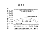
図19は図8、図9に示した設計例において、内側円形突出領域のみのNA値を変化させたときのCDでの規格化中心強度の変化を計算したものである。たとえばマレシャル条件までのマージンが半分になるまで劣化するずれを許容範囲と仮定すると、許容範囲はNA値で約±0.04であることがわかる。
【0039】
図20は図19と同様に、内側円形突出領域のみのNA値を変化させたとき、DVDの再生波面収差を計算した結果である。マレシャル条件が0.07λであることを考慮すれば、図19におけるCDの規格化中心強度の劣化に比べ、ずれに対する許容範囲が広く、上記±0.03のずれによりほとんど影響がないことがわかる。
【0040】
図21は図8、図9に示した設計例において、輪帯陥没領域内径のみのNA値を変化させたときのCDでの規格化中心強度の変化を計算したものである。たとえばマレシャル条件までのマージンが半分になるまで劣化するずれを許容範囲と仮定すると、許容範囲はNA値で約±0.03であることがわかる。
【0041】
図22は図21と同様に、輪帯陥没領域内径のみのNA値を変化させたとき、DVDの再生波面収差を計算した結果である。マレシャル条件が0.07λであることを考慮すれば、図19におけるCDの規格化中心強度の劣化に比べ、ずれに対する許容範囲が広く、上記±0.03のずれによりほとんど影響がないことがわかる。
【0042】
図23は図8、図9に示した設計例において、輪帯陥没領域外径のみのNA値を変化させたときのCDでの規格化中心強度の変化を計算したものである。たとえばマレシャル条件までのマージンが半分になるまで劣化するずれを許容範囲と仮定すると、許容範囲はNA値で約±0.02であることがわかる。
【0043】
図24は図23と同様に、輪帯陥没領域外径のみのNA値を変化させたとき、DVDの再生波面収差を計算した結果である。輪帯陥没領域外径については、円形突出領域径、輪帯陥没領域内径のずれの影響と異なり、輪帯陥没領域外径大きいほど収差は大きく、輪帯陥没領域外径が小さいほど小さくなっている。これは輪帯陥没領域外径が本実施例での設計においては最適基板厚変化の境界と一致させているためである。つまり輪帯陥没領域外径が大きいとそれだけCDに最適な基板厚に近づけた領域が広くなるので、DVDの収差は大きくなる。しかしこれによれば上記に述べた±0.02のずれに対しても波面収差は0.04λ以下であり、問題はないことがわかる。
【0044】
図25は図8、図9に示した設計例において、円形突出領域の位相シフト誤差に対する、CD−R用光スポットの規格化中心強度を示す。たとえばマレシャル条件までのマージンが半分になるまで劣化するずれを許容範囲と仮定すると、円形突出領域の位相シフトずれの許容誤差は約±0.1λであることがわかる。
【0045】
図26は図25と同様に、円形突出領域の位相シフトを変化させたとき、 DVDの再生波面収差を計算した結果である。これについても上記の±0.1λのずれに対して、DVDのRMS波面収差の劣化は0.01λ程度であり、ほとんど問題ないことがわかる。
【0046】
図27は図8、図9に示した設計例において、輪帯陥没領域の位相シフト誤差に対する、CD−R用光スポットの規格化中心強度を示す。たとえばマレシャル条件までのマージンが半分になるまで劣化するずれを許容範囲と仮定すると、輪帯陥没領域の位相シフトずれの許容誤差は円形突出領域と同様に約±0.1λであることがわかる。
【0047】
図28は図27と同様に、輪帯陥没領域の位相シフトを変化させたとき、 DVDの再生波面収差を計算した結果である。これについても上記の±0.1λのずれに対して、DVDのRMS波面収差の劣化は0.01λ程度であり、ほとんど問題ないことがわかる。
【0048】
また円形突出領域と輪帯陥没領域で位相差の絶対値を等しく、符号を反転させることを設計上仮定したものの、図25、26、27、28からわかるように、それぞれ単独の位相ずれを与えても、ほぼ設計形状で最適な値となっていたことがわかる。
【0049】
図29は図8、図9に示した設計例において、内側最適基板厚を変えたときのCD−R用光スポットの規格化中心強度を示す。たとえばマレシャル条件までのマージンが半分になるまで劣化するずれを許容範囲と仮定すると、−0.05mmであることがわかる。基板厚が厚くなる方向については、よりCDの最適基板厚に近づく方向であるので、規格化中心強度はかえって大きくなる。
【0050】
図30は図29と同様にして内側最適基板厚を変えたときの、DVD再生スポットのRMS波面収差の計算結果である。これについては図29と逆に基板厚が厚くなるとDVDの最適基板厚0.6mmからの差が大きくなる方向であるため、厚くなる方向で収差が大きくなっている。厚さが薄くなるとDVDの最適基板厚に近づくため、収差は小さくなる。これによればたとえばDVDのRMS波面収差を0.04λ程度を許容値とすれば+0.05mmであることがわかる。
【0051】
図29、図30より内側最適基板厚の許容誤差は±0.05mm程度であることがわかる。
【0052】
以上の最適形状の範囲、および誤差について図31にまとめる。図4、5、6、7に示したCDの有効NAに対する最適形状範囲の下限と上限を表の左側に示す。ここで下限、上限はCDでマレシャル条件を満たす有効NAの下限、および上限での設計値を示す。また図19から30に示した各パラメタの誤差の範囲を次の欄に示した。誤差はすでに述べたように、およそCD−R用光スポットのマレシャル基準までのマージンが半分に減少する範囲を示しており、DVDのRMS波面収差の増大はこの範囲でほぼ問題ないことを確認している。これらを合成したときの下限と上限を次の複合範囲の欄に示した。合成にあたってはこれらの広い方の範囲を選んでいる。したがって本発明が効果を発揮するためにとりうる各パラメタの範囲はこれらの範囲であることがわかる。
【0053】
また図32は図8、図9に示した設計例において、CD用の光の波長を変えたときのCD−R用光スポットの規格化中心強度を示す。これによればたとえばマレシャル条件までのマージンが半分になるまで劣化するずれを許容範囲と仮定すると、本実施例の設計仕様値である785nmからのずれが±15nm程度であることがわかる。これは通常の半導体レーザの仕様値に比べてほぼ十分な範囲である。
【0054】
図33はDVDの再生波長を変えたときの、DVDの再生波面収差を示している。これによればたとえばDVDでの許容波面収差を0.04λとすれば、本実施例の設計仕様値である655nmからのずれが±15nm程度であることがわかる。これは上記と同様に通常の半導体レーザの仕様値に比べてほぼ十分な範囲である。
【0055】
図34は図8に示した設計仕様に対するレンズの実形状の実施例である。設計にあたっては松居吉哉「レンズ設計法」(共立出版、1989年、初版第7刷)にもとづき、まずDVDの仕様に合わせて基板厚0.6mmに対して3次の球面収差と画角に対する3次のコマ収差が同時に0となるように第1面の周辺領域形状および第2面の曲率、非球面係数、肉厚を決めた。このときにはまだCD再生や、位相シフタの影響は何ら考慮しない。次に図8に示した波面収差形状において、位相シフタの寄与を除いた部分が得られるように第1面の内側領域の形状を、やはりまだ位相シフタの影響はのぞいて設計する。最適基板厚が変化する境界における輪帯陥没領域の位相シフト以外の位相、および境界の内外での近軸焦点位置の違いを満たす条件のもとに、図8の仕様の内側最適基板厚の平行平板を挿入したときに、上記と同様にして3次の球面収差が0となるように、第1面内側突出領域の曲率と非球面係数、肉厚を決めた。さらのこの形状に対して、図8に示した位相シフタを対物レンズの屈折率の値を考慮して段差の深さに換算し、指定された半径位置に設置する。このとき光線の進行方向を考慮して周辺部は段差の深さまたは方向を若干補正する。つまりレンズの光軸に対して平行に入射する入射光線も、光軸から離れた位置に入射する光線では第1面において斜めに屈折するため、そのような斜めの光線に対して所望の位相シフトを加えるためには実際上、光線の屈折方向にそって位相シフトを加えることが必要である。また本実施例においては第1面の内側領域の形状の計算においてコマ収差の影響を考慮していない。これを考慮するためには実際上、第2面にも内側領域を設ければよい。非球面対物レンズでは一般的に、球面収差と画角に対するコマ収差を同時に0とするには第1面、第2面の両面を非球面とすることが必要であり、内側最適基板厚において内側でも画角に対する3次のコマ収差係数を0とするにはやはり2面の専用の非球面が必要であることは必然である。したがって画角に対するコマ収差が問題となる場合には、両面で内側と外側で形状の異なるレンズとすればよい。図34では図中に示した第ν面の面形状式において、第1面外側(第1A面)、第1面内側(第1B面)、第2面の、曲率r1A、r1B、r2、4次の非球面係数b1A、b1B、b2、第1A面と第2面の近軸での面間隔d1A、第2A面と第2面の近軸での面間隔d1B、段差部の位相シフト以外の面不連続g、位相シフトs1、s2、位相シフトの境界半径R1、R2、R3、レンズの有効口径R、NA、などの計算結果を示している。
【0056】
図35は本発明による対物レンズを用いた光ヘッドの実施例である。波長650nmのDVD用半導体レーザ351からの光はビームスプリッタ352により反射されて、コリメートレンズ353により平行光とされ、反射ミラー354により反射され、本発明による対物レンズ355により、基板厚さ0.6mmのDVDディスク356の記録膜面に集光される。一方、波長780nmのCD用半導体レーザ357からの光は、まず3ビーム方式によるトラッキング信号を得るために設置された回折格子358を透過し、ハーフミラー359の表面で反射され、ビームスプリッタ352を透過し、コリメートレンズにより平行光とされ、反射ミラー354を反射し、本発明による対物レンズ355により基板厚さ1.2mmのCDディスク3510の記録膜面に集光される。回折格子によるサブスポットは0次光に対してディスク半径方向に1/2トラックずれて配置されるように回折格子の光軸まわりの回転角度を調整しておく。なおCDのトラッキングはプッシュプル方式と呼ばれるトラッキングも規格上可能であり、これのみを用いる場合には回折格子は不要となる。なお反射ミラー354は図では便宜上、上方に反射する配置としているが、実際には紙面に垂直な方向に反射させるのが光ヘッドの配置上望ましい。このとき基板厚さの違いにより、記録膜面の位置はDVDディスク356とCDディスク3510で、基板厚差×(基板屈折率−1)だけ光軸方向にずれている。基板屈折率は約1.58であるから、これは約0.35mmである。したがって対物レンズの表面からディスク基板表面までの距離、すなわちワーキングディスタンスは0.25mmずれている。DVDおよびCDディスクを反射した光は同じ光路を戻り、まず対物レンズ355で再び平行光とされ、反射ミラー354を反射し、コリメートレンズ353で収束光となり、ビームスプリッタ352、ハーフミラー359を透過して光検出器3511に集光される。ここでハーフミラー359は平行平板で形成されており、収束光が透過する場合、非点収差を発生する。この非点収差を非点収差焦点ずれ検出方式に利用して、焦点ずれ信号を検出する。そのため光検出器3511の受光面は4分割された光検出領域を持ち、これらの演算により、焦点ずれ信号のみならず、トラッキング誤差信号も検出し、これらのスポット位置制御信号を、対物レンズ355を搭載した対物レンズアクチュエータ3512の駆動信号とすることで、焦点位置制御を行なう。ここでビームスプリッタ352は光利用効率の点では、ダイクロイック偏光ビームスプリッタであることが望ましい。すなわち半導体レーザ351からの650nmの光はビームスプリッタ352に入射するにあたってS偏光となるように配置し、ほぼ100%反射させる。そして図中に示していないが、コリメートレンズ353から対物レンズ355の間にλ/4板を挿入しておき、ディスクに集光される光を円偏光となるようにする。すると反射光が再びλ/4板を透過したとき入射時と直交する偏光方向の直線偏光、すなわちS偏光となってビームスプリッタ352に入射する。するとS偏光はほぼ100%透過して、光検出器3511に集光されることになる。一方波長780nmのCD用半導体レーザからの光は、ビームスプリッタを透過させないといけないため、780nmの光では透過率をなるべく100%に近づけるようにする。また780nmについては反射光もやはり透過させる必要があるため、ビームスプリッタ352は780nmでは偏光方向によらず透過率が100%に近いことが望ましい。なお以上のような2つの半導体レーザの配置は必ずしも固定したものではない。光利用効率の設計上、半導体レーザ351の位置の方が効率が高く、CD−Rの記録のために780nmの波長の方でより光利用効率を高くする必要がある場合、半導体レーザ351を780nmとすることも有効である。ただしこのとき回折格子358は半導体レーザ351とビームスプリッタ352の間に挿入する必要がある。また逆に波長650nmでもDVD−RAMなどの記録を行なう必要があり、CD−R記録よりも高い光利用効率が必要な場合には本実施例で説明したように半導体レーザ351を650nmとするのが有効である。
【0057】
また本発明における対物レンズでは、780nmの光も650nmの光も対物レンズに平行光束として入射することを想定している。このため反射光は2つの波長でほとんど同一の光路を戻るため、本実施例に示すように1つの光検出器3510での検出が可能となる。従来例において述べたように対物レンズに入射する光束の収束、発散の状態を2つの波長で異ならせることで対物レンズで発生する球面収差を用いて基板厚誤差による球面収差を補償する方法では、当然ながら反射光束の光路が2つの波長で異なることになる。したがってこのような従来の方法では光検出器を1つにすることができないので、製造コストの点でも不利となる。
【0058】
ただし本発明は必ずしも2つの波長がともに平行光である必要もまたない。すなわち2つの波長の対物レンズへの入射光の収束、発散状態を、半導体レーザと対物レンズの相対的な位置ずれの許容範囲を満たす範囲内でずらし、多少この効果によって基板厚ずれによる球面収差の補償効果を満たした上で、本発明による対物レンズでさらに残りの球面収差を補償すればよい。このような設計はまた十分可能である。
【0059】
図36は光検出器361における検出信号から再生信号(RF信号)、焦点ずれ信号(AF信号)、トラッキング誤差信号(TR信号)を得る方式について説明する図である。焦点ずれ検出方式としては非点収差法による信号、トラッキング信号は、プッシュプル方式によるトラッキング誤差信号(PP信号)、位相差検出方式によるトラッキング信号(DPD信号)、3ビーム方式によるトラッキング誤差信号(3ビーム信号)の3種類の信号を検出する実施例を示している。検出器361には4分割受光領域362、サブスポット用検出領域363、364がある。各受光領域からの光は電流電圧変換アンプ365で電圧に変換され、抵抗366をへて差動アンプ367に入力され、各種信号演算に用いる。
【0060】
RF信号はメインスポット368の総光量を出力しており、演算は4分割検出領域362の各出力をすべて加算するように演算を行なっている。
【0061】
AF信号は非点収差焦点ずれ検出方式による実施例を示しており、メインスポット368を受光する4分割検出領域362の対角方向の2領域を加算し、それぞれ2組の加算結果の差を演算する構成となっている。非点収差検出方式は検出光束に非点収差を与えて、焦点の前後で直交する直線状の焦線を生じることを用いて検出する方式である。
【0062】
PP信号は記録可能な光ディスクにおいて主に用いられる検出方式であり、ディスク上に周期的に作られた案内溝による回折光どうしの干渉強度が、集光スポットと案内溝との相対的な位置ずれによりアンバランスを生じることを用いて検出する方法である。具体的にはDVD−RAMディスクや、光磁気ディスク、CD−Rなどが該当する。また先に述べたように、規格上CDのトラッキングに対しても用いられることが規定されている。信号の演算はメインスポット368を受光する4分割検出領域の半径方向の分割線で分割されるそれぞれの2領域ごとの出力を加算し、その差を演算してトラッキング誤差信号とする。ここで検出器上の分布は非点収差により、非点収差付加の前の分布から、90°回転している。
【0063】
DPD信号はDVD―ROMディスクで用いられている方法であり、ディスク上の光スポットが情報トラックからずれている場合、検出光束上でディスク半径方向と接線方向で分割される4領域の対角方向の2領域ごとの情報ピットによる検出光量変化に生じる時間遅れを検出する方法である。規格上、現状はDVD−ROM、記録後のDVD−Rでしか規定されていないが、原理的にはCDでも検出可能である。信号の演算はメインスポット368を受光する4分割光検出領域の対角方向でない、2組の2領域ごとの出力の位相差を位相差検出回路3611、3612で検出して電圧として出力し、これらの差の演算を行なうことによりトラッキング信号とする。
【0064】
3ビーム信号は現状CDで広く用いられている方法であり、すでに述べたように回折格子により2つのサブスポットをディスク上にメインスポットの半径方向両側に1/2トラックずれて配置させ、メインスポットが情報トラックからずれているときに2つのサブスポットの検出光量に生じるアンバランスを検出する方法である。信号の演算は、2つのサブスポット369、3610の受光領域363、364の出力の差を演算することにより得られる。
【0065】
図37に本発明による光ヘッドを光ディスク装置に用いた場合の実施例を示す。
【0066】
光ディスク装置3700は、光ヘッド3701と、制御回路、及び、モータなどの機構系から構成されている。光ヘッド3701からの電気的な入出力はフレキシブル基板3702、3703を介して行われる。本実施例においては半導体レーザ3704、3705の駆動をフレキシブル基板3702、光検出器3706の入出力をフレキシブル基板3703によって行っている。
【0067】
半導体レーザ3704、3705はユーザデータ3707をストアしたバッファメモリ3708のディジタル情報に応じて生成された、記録波形発生回路3709からの記録波形によりレーザ駆動回路3710で、その明滅を制御する。
【0068】
光検出器3706による電流出力は信号演算回路3711によって電流電圧変換され、増幅され、本発明の演算方法によって演算され、焦点ずれ誤差信号、トラッキング誤差信号、ヘッド位置制御信号を生成する。前記2つの誤差信号は対物レンズアクチュエータ3712にフィードバックされ、集光スポットが光ディスク3713の記録膜面の情報トラックの上に常にあるように閉ループ制御される。他方、ヘッド位置制御信号はディスクのアドレス情報ピットから、RF信号によって検出され、光ヘッド3701を再生トラックの近傍にほぼ配置させるよう、ヘッド移動機構3714に入力される。こちらの制御はディジタル情報記録用の光磁気ディスクの場合にはやはり通常、閉ループ制御されるが、CD、DVD、MDなどにおいては開ループ制御させることが多い。
【0069】
信号演算回路3711において得られたRF信号は信号処理回路3715においてイコライザ処理、2値化、復号処理されディジタル情報を再生する。出力情報はバッファメモリ3708にストアされる。
【0070】
光ディスク3713はスピンドルモータ3716で回転されており、スピンドルモータ駆動回路3717によってその回転が制御されている。さらにこれらすべての制御回路はコントローラ3718で制御されている。
【0071】
本実施例においては、記録可能な光ディスクを例としたが、CD−ROMや、DVD−ROMなど再生専用光ディスクにおいても、記録制御系が不要となるだけでそれ以外はほぼ同様の構成で光ディスク装置を実現できる。
【0072】
本発明による光ヘッドを用いることで、光ディスク3713としてDVD再生、CD再生、DVD−RAM記録再生、CD−R記録再生が可能な光ディスク装置を実現できる。
【0073】
【発明の効果】
本発明により、CD再生、CD−R記録再生、DVD−ROM再生、DVD−RAM記録再生が可能な対物レンズが実現できる。
【図面の簡単な説明】
【図1】 DVD/CD−R互換レンズ従来例を示す図。
【図2】 DVD/CD−R互換レンズ従来例における波面収差を示す図。
【図3】 本発明による対物レンズの概略形状を示す図。
【図4】 従来設計と本発明のCDスポット規格化中心強度の比較を示す図。
【図5】 本発明における内側円形突出領域、輪帯陥没領域内径、輪帯陥没領域外径の設計値を示す図。
【図6】 本発明における輪帯陥没領域の位相シフト量の設計値を示す図。
【図7】 本発明における内側領域の最適基板厚の設計値を示す図。
【図8】 本発明による対物レンズの波面収差形状例を示す図。
【図9】 本発明による第2の対物レンズの波面収差形状例を示す図。
【図10】 通常のCD−R記録スポットプロファイルの計算結果を示す図。
【図11】 図8の波面収差形状を与える本発明の対物レンズによるCD−R記録用スポットプロファイルの計算結果を示す図。
【図12】 通常のDVD専用対物レンズによるDVD再生光スポットプロファイルの計算結果を示す図。
【図13】 図8の波面収差形状を与える本発明の対物レンズによるDVD再生用スポットプロファイルの計算結果を示す図。
【図14】 図10に示した通常のCD−R用対物レンズによる光スポットによるCD−ROM再生信号アイパターン計算結果を示す図。
【図15】 図11に示した本発明による対物レンズによる光スポットによるCD−ROM再生信号アイパターン計算結果(検出NA0.6)を示す図。
【図16】 図11に示した本発明による対物レンズによる光スポットによるCD−ROM再生信号アイパターン計算結果(検出NA0.5)を示す図。
【図17】 図12に示した通常のDVD用対物レンズを用いた光スポットによるDVD−ROM再生信号アイパターン計算結果を示す図。
【図18】 図13に示した本発明による対物レンズを用いた光スポットによるDVD−ROM再生信号アイパターン計算結果を示す図。
【図19】 図8、図9に示した設計例における内側円形突出領域NA値に対するCD−R用スポット規格化中心強度を示す図。
【図20】 図8、図9に示した設計例における内側円形突出領域NA値に対するDVD再生RMS波面収差を示す図。
【図21】 図8、図9に示した設計例における輪帯陥没領域内径NA値に対するCD−R用スポット規格化中心強度を示す図。
【図22】 図8、図9に示した設計例における輪帯陥没領域内径NA値に対するDVD再生RMS波面収差を示す図。
【図23】 図8、図9に示した設計例における輪帯陥没領域外径NA値に対するCD−R用スポット規格化中心強度を示す図。
【図24】 図8、図9に示した設計例における輪帯陥没領域外径NA値に対するDVD再生RMS波面収差を示す図。
【図25】 図8、図9に示した設計例における円形突出位相シフト領域の位相シフト誤差に対するCD−R用光スポット規格化中心強度を示す図。
【図26】 図8、図9に示した設計例における円形突出領域の位相シフト誤差に対するDVD再生RMS波面収差を示す図。
【図27】 図8、図9に示した設計例における輪帯陥没領域の位相シフト誤差に対するCD−R用光スポット規格化中心強度を示す図。
【図28】 図8、図9に示した設計例における輪帯陥没領域の位相シフト誤差に対するDVD再生RMS波面収差を示す図。
【図29】 図8、図9に示した設計例における内側最適基板厚誤差に対するCD−R用光スポット規格化中心強度を示す図。
【図30】 図8、図9に示した設計例における内側最適基板厚誤差に対するDVD再生RMS波面収差を示す図。
【図31】 最適形状の範囲と誤差をまとめた表。
【図32】 図8、図9に示した設計例におけるCD−R用波長誤差に対するCD−R用光スポット規格化中心強度を示す図。
【図33】 図8、図9に示した設計例におけるDVD用波長誤差に対するDVD再生RMS波面収差を示す図。
【図34】 図8に示した設計仕様に対するレンズの実形状を示す図。
【図35】 本発明による対物レンズを用いた光ヘッドを示す図。
【図36】 光検出器からの信号演算方法を説明する図。
【図37】 本発明による対物レンズを用いた光ヘッドを搭載した光ディスク装置の実施例。
【符号の説明】
1…DVD/CD−R再生互換対物レンズ、12…外側領域、13…輪帯位相シフタ、14…エッジ部分、3…本発明によるDVD/CD−R記録互換対物レンズ、31…輪帯陥 没領域、32…円形突出領域、351… DVD用半導体レーザ、352…ビームスプリッタ、353…コリメートレンズ、354…反射ミラー、355…本発明による対物レンズ、356…DVDディスク、357…CD用半導体レーザ、358…回折格子、359…ハーフミラー、3510…CDディスク、3511…光検出器、3512…対物レンズアクチュエータ、361…光検出器、362…4分割受光領域、363、364…サブスポット用検出領域、365…電流電圧変換アンプ、366…抵抗、367…差動アンプ、368…メインスポット、369、3610…サブスポット、3611、3612…位相差検出回路、3700…光ディスク装置、3701…光ヘッド、3702、3703…フレキシブル基板、3704、3705…半導体レーザ、3706…光検出器、3707…ユーザデータ、3708…バッファメモリ、3709…記録波形発生回路、3710…レーザ駆動回路、3711…信号演算回路、3712…対物レンズアクチュエータ、3713…光ディスク、3714…ヘッド移動機構、3715…信号処理回路、3716…スピンドルモータ、3717…スピンドルモータ駆動回路、3718…コントローラ。[0001]
BACKGROUND OF THE INVENTION
The present invention,versusIn particular, the present invention relates to compatible reproduction of optical disks having different substrate thicknesses.
[0002]
[Prior art]
In recent years, the density of optical disks has been increasing, and 4.7 GB DVD-ROMs have been put on the market as compared to 0.65 GB CD-ROMs that are consumer-use reproduction-only optical disks. However, the thickness of the substrate differs between DVD and CD, which is 0.6 mm for DVD and 1.2 mm for CD. Such a difference is that, for the purpose of improving the recording density, the sin value of the lens condensing angle which is an index of the condensing power of the objective lens, that is, the numerical aperture (NA) is larger than 0.45 of CD in DVD. This is because the occurrence of aberration due to disc tilt or the like was suppressed because of 0.6. In a DVD drive device, it is considered essential to reproduce a CD, and such a difference in disc substrate thickness causes a problem in selecting a corresponding substrate thickness of the objective lens.
[0003]
First, the meaning of the corresponding substrate thickness will be described. In an optical disk, in order to prevent recording information from being reproduced due to dust or the like, usually, light is condensed and reproduced from the back side of a transparent substrate such as polycarbonate having a recording surface to the recording film surface through the substrate. In this way, for example, in the case of a DVD with a substrate thickness of 0.6 mm, the light spot on the surface of the substrate is about 0.5 mm, and if the dust is about 0.1 mm or less, the reading will be greatly affected. Absent. As a result, unlike the magnetic disk, the user can replace the disk by himself and play it. However, when the light is collected through the substrate in this way, the objective lens needs to be shaped according to the thickness of the substrate. For example, when a transparent substrate having a certain thickness is inserted into an ideally condensed light beam, the latter is naturally the latter for light incident perpendicularly to the substrate and light incident obliquely. The light path inside becomes longer. Such an optical path difference is called an aberration, which causes the light to be unable to be focused. However, such aberration can be compensated by the shape of the lens if the thickness of the substrate to be inserted is known in advance. Therefore, in the optical head of the optical disc apparatus, the substrate thickness of the optical disc to be normally reproduced is specified, and an objective lens corresponding to the substrate thickness is used. As described above, the corresponding substrate thickness is a thickness of a substrate that can ideally collect light without causing aberration by being inserted into a condensed light beam by a certain objective lens.
[0004]
As described above, since the corresponding substrate thickness is determined for each normal objective lens for an optical disk, there has been a problem in compatible reproduction between DVD and CD.
[0005]
On the other hand, for example, in Japanese Patent Laid-Open No. 6-124477, liquid crystal is used to limit the aperture in CD reproduction and to shield the peripheral part having large aberration, so that the aberration due to the substrate thickness error in CD reproduction by the DVD lens can be prevented. It was reduced. The aberration caused by the substrate thickness error is called spherical aberration and increases in proportion to the fourth power of NA. Therefore, when the NA is reduced by the aperture, the aberration is also reduced. On the other hand, in DVD reproduction, the presence or absence of an opening is used repeatedly so as not to block light. Here, this conventional example is intended to reproduce a CD at a reproduction wavelength of 650 nm for DVD. That is, the wavelength is shorter than the wavelength 780 nm used for the conventional CD. If the wavelength of the focused spot is λ, it is proportional to λ / NA. Therefore, if the wavelength is short, the required NA can be reduced. Therefore, as a result, the CD reproduction is performed at 650 nm, so that the NA of the aperture can be made smaller than 0.45, thereby obtaining the necessary aberration reduction effect in the conventional example. However, the conventional example has a problem that it is compatible with a CD and cannot cope with a writable CD-R (CD-Recordable) that has been widely spread recently. This is because CD-R uses a dye medium having a sufficient reflectance only at 780 nm for the recording film, and the reflectance decreases at a DVD reproduction wavelength of 650 nm, and signal reproduction is impossible. In order to reproduce the CD-R, it is necessary to separately mount a light source of 780 nm on the optical head. At this time, since the wavelength is the same as that of the conventional CD, the NA of the limiting aperture needs to be 0.45 or more of the conventional aperture, and a sufficient aberration reduction effect cannot be obtained.
[0006]
As another conventional example, Japanese Patent Application Laid-Open No. 9-237431 describes a method of shielding light in an annular region. This is a method of removing only the region that directly deteriorates the light spot of the CD reproduction by shielding the light in the annular zone where the aberration starts to change greatly when the CD is reproduced by the DVD lens. This is because the light beam in the region where the aberration is very large and the wavefront inclination is large travels in the direction perpendicular to the wavefront, so that it largely dissipates from the focal position and does not affect the spot performance. In DVD reproduction, light inside and outside the ring-shaped light shielding region is condensed with substantially no aberration. At this time, the light in the annular shield region is shielded even during DVD reproduction, but by making the region narrow to an allowable range, substantially the same effect can be obtained without using an element such as liquid crystal. However, on the contrary, since it is substantially equivalent to restricting the opening, this also has a problem that it cannot cope with CD-R reproduction by 780 nm.
[0007]
Still another conventional technique is described in JP-A-8-55363. Here, two types of optical disks with different substrate thicknesses are reproduced with light sources of different wavelengths, and the distance from the two semiconductor laser lenses is changed to shift the state of divergence or convergence of the light incident on the objective lens. ByBaseA method for compensating for spherical aberration due to thickness deviation is described. If this method is used, a 780 nm semiconductor laser is used for CD playback and a 650 nm semiconductor laser is used for DVD playback, so that DVD and CD can be played back with a single objective lens, and CD-R playback is also possible. However, it is known that if the positions of the two light sources are made different in this way, the allowable range of relative positional deviation between the semiconductor laser and the objective lens is narrowed. This is because in the design of an objective lens, there is a condition called a sine condition as a condition that coma aberration does not suddenly occur even if the incident angle of the incident light is deviated, but this is true only at a specific distance between object images. This is because it is impossible to achieve the distance between the two types of object images. That is, for example, if the sine condition is satisfied in the arrangement of the semiconductor laser having the wavelength of 650 nm, the arrangement of the semiconductor laser having the wavelength of 780 nm cannot satisfy this condition. In this case, for example, if the disk is decentered and rotated, the objective lens will follow and move during tracking control, and the relative position with respect to the semiconductor laser will shift and abrupt aberrations will occur.
[0008]
Still another conventional technique is described in, for example, Japanese Patent Laid-Open No. 10-255305 by the present inventors. Here, as shown in FIG. 1, an annular phase shifter formed of a concave groove-shaped concave portion on a lens having a corresponding substrate thickness of 0.76 mm in the
[0009]
FIG. 2 shows calculated values of wavefront aberration during DVD reproduction and CD reproduction in the conventional example. Here, the wavefront aberration represents an error in the optical path length from the semiconductor laser as the light source to the objective lens with respect to the light ray position in the effective luminous flux (pupil) of the lens. However, in FIG. 2, the range in which the aberration exceeds ± 0.5λ is displayed by being folded into the range of ± 0.5λ, which is a substantially equal phase value. The phase shift amount of the annular phase shifter is set to -1.76λ in the CD reproduction. Here, the negative phase shift means that the optical path length is shortened, and indicates that the step is concave. Then, in CD, a positive phase shift of 0.24λ obtained by adding 2 so that the phase shift amount after the decimal point is in the range of ± 0.5λ is added. On the other hand, in DVD reproduction, the refractive index is 1.583 at a wavelength of 780 nm, 1.586 at 650 nm, and -1.76 / (1.583-1) × 780/650 × (1.586-1) = − 2.12λ It becomes. Also in this case, when 2 is added so that the phase shift amount is in the range of ± 0.5λ, −0.12λ is obtained, and a negative phase shift as shown in FIG. 2 is added. Such an effect is not equivalent when the annular phase shifter is concave or convex because the sign of the phase shift required for each wavelength is determined. For example, in order to realize a phase shift amount substantially equal to the above with a convex phase shifter, assuming that the CD phase shift amount is + 3.24λ, 3.24 / (1.583-1) × 780/650 × (1 .586-1) = 3.91λ, and 4 is subtracted to be −0.09λ so that the phase shift amount is in the range of ± 0.5λ. However, when the absolute value of the phase shift including the integer part becomes large in this way, the level difference becomes deep and processing becomes difficult, and the error of the phase shift amount due to wavelength shift due to temperature fluctuation increases in proportion to the integer part. To do. Therefore, it is desirable that the step is concave here. With respect to the wavefront aberration obtained as shown in FIG. 2 as described above, for example, an RMS value is 0.07λ or less (λ is a light wavelength) or less in order for a light spot to be favorably focused according to the Marechal criterion. It is necessary to be. On the other hand, in the DVD reproduction, the RMS wavefront aberration is 0.02λ, and the performance is good. In CD reproduction, the wavefront aberration is very large in the peripheral portion, but the above criteria are satisfied in the range of NA effective in design. Light having a large aberration at the peripheral portion is easily dissipated because the wavefront has a very large inclination, and there is substantially no influence on the light spot only by the central portion. In this way, compatible playback was realized in DVD, CD, and CD-R playback.
[0010]
[Problems to be solved by the invention]
In the above conventional example in which the annular phase shifter is integrally formed with the objective lens, there is a problem that only the reproduction of CD-R is supported, and the CD-R recording apparatus does not sufficiently reduce the aberration. This is because the CD-R recording apparatus uses an objective lens with an NA of 0.5, which is larger than the reproduction NA, in order to record a recording mark equivalent to the recording information pit of the CD with high accuracy. Since the above conventional example only considers reproduction with respect to the CD-R, only a light spot equivalent to a CD-ROM optical pickup having a wavelength of 780 nm and NA of 0.45 can be formed. Accordingly, the aberration increases in the range of NA 0.5, and it cannot cope with CD-R recording.
[0011]
In view of the above problems, the problem to be solved in the present invention is an objective lens that achieves both DVD reproduction and CD-R recording.TheIs to realize.
[0012]
[Means for Solving the Problems]
In order to solve the above-mentioned problem, in the objective lens according to the conventional example having at least two refracting surfaces, a circular region near the optical axis of the lens protrudes with a step on at least one of the two surfaces. IeIt is an annular depression areaInverted phase shifter and shift directionCircular protruding areaAdd a circular phase shifter. In this manner, the unevenness of the wavefront aberration in the central region in FIG. 2 can be reduced, the RMS wavefront aberration can be reduced, the effective light beam in CD reproduction can be expanded, and the light spot performance necessary for CD-R recording can be realized.
[0013]
At this time, as described in the conventional example, at least the circular shapeProtrusionIn the region, the optimum substrate thickness is set to a substrate thickness closer to the CD substrate thickness of 1.2 mm than the DVD substrate thickness of 0.6 mm. That is, in this region alone, aberrations are smaller when reproducing an optical disc with a substrate thickness greater than 0.6 mm than when reproducing an optical disc with a substrate thickness of 0.6 mm. Also at the same timeSinkingIn the region outside the region, the corresponding substrate thickness is set to 0.6 mm so as to be optimal for the DVD. That is, when reproducing an optical disk having a substrate thickness of 0.6 mm, the shape with the smallest aberration is used.
[0014]
More specifically, the circular shape for the total effective light beam diameter.ProtrusionThe incident light beam diameter ratio to the region is R1, and the ring zoneSinkingThe luminous flux diameter ratio applied to the inner diameter of the region is R2, and the annular zoneSinkingWhen the light beam diameter ratio over the outer diameter of the region is R3,
0.22 ≦ R1 ≦ 0.35, 0.40 ≦ R2 ≦ 0.50, 0.75 ≦ R3 ≦ 0.82, R1 ≦ R2 ≦ R3
It is effective to satisfy.
[0015]
In such an objective lens, at least the inner circleProtrusionIf the substrate thickness with the smallest aberration in the region is 0.74 mm or more and 0.85 mm or less, the effect is greater.
[0016]
In addition, by combining such an objective lens with a semiconductor laser of at least two wavelengths and a lens, prism, mirror, photodetector, etc., an optical head can be constructed for the first time to achieve both DVD playback and CD-R recording. It becomes a simple optical head.
[0017]
Furthermore, in the objective lens used for the optical head equipped with such a two-wavelength light source,ProtrusionArea, and ring zoneSinkingThe optical path length differences caused by the step in the region are φ1 and φ2, respectively, and when the longer wavelength of the two wavelengths, that is, the CD reproduction wavelength is λ1, 1.67λ1 ≦ φ1 ≦ 1.87λ1, −1.87λ1 ≦ φ2 ≦ − 1.67λ1
It is effective to satisfy.
[0018]
At this time, when the shorter wavelength of the two wavelengths, that is, the DVD reproduction wavelength is λ2, 2.00λ2 ≦ φ1 ≦ 2.24λ2 and −2.24λ2 ≦ φ2 ≦ −2.00λ2 are satisfied.
[0019]
Also, DVD playback and CD-R recording are made compatible for the first time by configuring an optical head integrally with an objective lens having these steps, a semiconductor laser of at least two wavelengths, and a lens, prism, mirror, photodetector, etc. It becomes an optical head capable of.
[0020]
In addition, such an optical head can be used for DVD reproduction and CD-R for the first time by forming an optical disk apparatus integrally with a mechanism and a control circuit that can reproduce or record / reproduce optical disks having at least two kinds of substrate thicknesses together. An optical disc apparatus capable of both recording is obtained.
[0021]
DETAILED DESCRIPTION OF THE INVENTION
Hereinafter, embodiments of the present invention will be described with reference to the drawings.
[0022]
FIG. 3 is a diagram showing a schematic shape of the
[0023]
Fig. 4 shows the method of using the annular phase shifter described in the above-mentioned conventional example by changing the reproduction wavefront aberration tolerance for DVD with respect to the effective NA at the time of CD reproduction, and the design standard for this new shape It is the graph which showed the conversion center intensity | strength. The CD reproduction wavelength is 0.785 μm, the DVD reproduction wavelength is 0.655 μm, the DVD reproduction NA is 0.6, the substrate thickness is CD 1.2 mm, and DVD 0.6 mm. For optimization, circularProtrusionArea and ring zoneSinkingThe absolute value of the phase difference in the region is equal and circularProtrusionPositive in area (increased optical path length), zonal zoneSinkingIn the region, a negative phase shift (optical path length reduction) is given, and the boundary of the change in the optimum substrate thickness is the annular zoneSinking areaIt matches the outer diameter. Here, the normalized center intensity is the ratio of the center intensity of the focused spot to the total light quantity of uniform intensity incident within the effective NA range, as described in the conventional example, Japanese Patent Laid-Open No. 10-255305. In this figure, the so-called Strehl strength is multiplied by the square of the ratio of effective NA to total NA. The Strehl intensity is 1− (2πWrms / λ) where RMS wavefront aberration is Wrms and wavelength is λ.2It is said that the Strehl intensity of 0.8 or more, that is, Wrms ≈ 0.07λ or less is necessary in the Marechal standard, which is the standard of the allowable range of aberration. However, in order to determine the optimum limiting aperture NA in the presence of aberration, mere Strehl intensity is not appropriate as an evaluation index. This is because the Strehl intensity is an evaluation criterion for aberrations when the NA is fixed, and the quality of light spots with different NAs cannot be evaluated as in this case. The larger the NA, the smaller the light spot when there is no aberration, so the light spot as a base becomes smaller. However, the larger the NA, the larger the aberration, so the spot deterioration becomes more remarkable. Accordingly, there should be an optimum NA in terms of the balance between aberration and NA, and the above normalized central intensity is used here as an evaluation index. For example, the normalized center intensity with no aberration at NA 0.6 is 1 and the light spot for CD-R recording with no aberration is NA 0.5 with no aberration, so the normalized center intensity is (0.5 / 0.6). )2= 0.694. When there is a Marechal reference aberration in the light spot for CD-R recording, this is 0.8 times, which is 0.556. Therefore, the normalized center intensity needs to be 0.556 or more for a light spot with aberration. In FIG. 4, the level of this aberration-free CD-R recording spot is indicated by a thick solid line, and the marshal reference is indicated by a broken line. There are two large sets of design value curves. One set does not exceed the broken line even at the peak, while the other set exceeds the broken line in the range of NA 0.48 to 0.53. The former is a value according to the conventional design, and the latter is a calculation result by the new design method according to the present invention. Each of the plurality of curves has different RMS aberration values allowed for DVD reproduction, and are 0.029λ, 0.025λ, and 0.021λ, respectively, from the top. This value is sufficiently smaller than the Marechal standard, and is acceptable as a design residual aberration. Of course, the larger the allowable aberration value of the DVD, the higher the quality of the CD reproduction spot and the greater the standardized center strength. As described above, in the present invention, it is understood that when the effective NA of the CD light spot is about 0.51, a light spot exceeding the Marshall standard of the CD-R recording light spot can be realized.
[0024]
FIG. 5 shows the inner circle in the new shape design of FIG.ProtrusionArea, ring zoneSinkingArea inner diameter, ring zoneSinkingThe design value of the region outer diameter is shown, and the vertical axis represents the region boundary with the NA value. In FIG. 4, design values with different allowable aberration values in DVD reproduction in FIG. According to this, it can be seen that the region boundary position hardly depends on the allowable aberration value in DVD reproduction. These values that are above the Marechal condition areProtrusionThe area is about 0.14 to about 0.20 in NA value.SinkingInside is about 0.25 to about 0.29, ring zoneSinkingThe outer diameter is in the range of about 0.45 to about 0.49. Ring zone with NA 0.42 or lessSinkingThe inner and outer diameters are the sameSinking areaIn the case where no exists, the normalized center strength is high, and the numerical value in this case is a value that matches the effective NA.
[0025]
FIG. 6 shows an annular zone in the design of the present invention shown in FIG.SinkingThe phase shift amount of the part is shown. In addition, as already mentioned, circularProtrusionPhase shift in regionamountIs a ringSinking areaAnd the absolute value are equal and the sign is inverted. According to this, the phase shift amount varies depending on the allowable aberration amount at the time of DVD reproduction, and in the range of 0.021λ to 0.029λ, the phase shift amount is about −1.81 to about −1.81 to about λ with a CD reproduction wavelength of 0.785 μm. It exceeds the Marechal condition in the range of -1.74λ.
[0026]
FIG. 7 shows the optimum substrate thickness for the inner region in the design of the present invention of FIG. As already mentioned here, the boundary of the optimum substrate thickness change is the annular zone.Sinking areaThe outer diameter is matched. According to this, it can be seen that the inner optimum substrate thickness varies depending on the allowable aberration amount during DVD reproduction, and is in the range of about 0.85 to 0.74 mm in the range of 0.021λ to 0.029λ. As the allowable aberration of DVD is larger, the shape suitable for CD is allowed, so that the inner optimum substrate thickness is closer to 1.2 mm. Further, the smaller the effective NA for CD reproduction, the narrower the area for CD, so that the inner substrate thickness is allowed to be a value close to 1.2 mm.
[0027]
FIG. 8 is a wavefront aberration shape in a design example in which a result with the highest normalized center intensity is searched when the DVD wavefront aberration allowable value is 0.029λ in FIG. At this time, the effective NA of the CD was 0.509. It can be seen that although the stepped portion is increased as compared with FIG. 2, the low aberration region in the CD is enlarged. At this time, the inner optimal substrate thickness is 0.81 mm, and the phase shift amount in CD is circular.Of the protruding areaWith phase shifter 1.781λ, ring zoneOf the depressed areaPhase shifter is -1.781λ, DVD phase shift is circularOf the protruding area2.134λ with a phase shifterOf the depressed areaThe phase shifter is -2.134λ. These are circular when 2 is added or subtracted to the integer part so that the decimal part is ± 0.5λ or less.Of the protruding areaPhase shifter -0.219λ, ring zoneOf the depressed areaPhase shifter is 0.219λ, DVD phase shift is circularOf the protruding areaPhase shifter 0.134λ, ring zoneOf the depressed areaThe phase shifter is -0.134λ. In the graph, this value substantially affects the phase shift. The boundary NA is circular.Of the protruding area0.182 phase shifter outer edge, ring zoneOf the depressed areaPhase shifter inner diameter is 0.275, ring zoneOf the depressed areaThe outer edge of the phase shifter is 0.475, and the CD-R recording NA is 0.509.
[0028]
FIG. 9 is intended to slightly improve the wavefront aberration of the DVD from the embodiment of FIG. 8, and the maximum value of the normalized central intensity in the CD reproduction when the DVD allowable wavefront aberration is 0.025λ in FIG. It is a wavefront aberration shape in the design example obtained as a result. At this time, the inner optimum substrate thickness is 0.78 mm, and the phase shift amount in CD is circular.Of the protruding area1.78λ with phase shifter, ring zoneOf the depressed areaThe phase shifter is -1.78λ, and the phase shift amount in DVD is circular.Of the protruding area2.133λ with a phase shifterOf the depressed areaThe phase shifter is -2.133λ. These are circular when 2 is added or subtracted to the integer part so that the decimal part is ± 0.5λ or less.Of the protruding areaPhase shifter -0.22λ, ring zoneOf the depressed areaPhase shifter is 0.22λ, DVD phase shift is circularOf the protruding areaPhase shifter with 0.133λ, ring zoneOf the depressed areaThe phase shifter is -0.133λ. The boundary NA is circular.Of the protruding area0.183 phase shifter outer edge, ring zoneOf the depressed areaPhase shifter inner diameter is 0.272, ring zoneOf the depressed areaThe outer edge of the phase shifter is 0.475, and the CD-R recording NA is 0.51.
[0029]
FIG. 10 shows the calculation result of the spot profile on the disk surface in the conventional optical head for CD-R recording. Here, for the same profile, the left is a bird's eye view and the right is a contour map. Here, it is assumed that the intensity distribution at the lens edge of the wavelength 785 nm, NA 0.5, and incident light (rim intensity) is 0.76 on the x side and 0.15 on the y side, and the intensity distribution is a Gaussian distribution. The numerical values below the contour map are the spot diameter and the side lobe intensity, WHX is the full width at half maximum in the x direction, WHY is the full width at half maximum in the y direction, WEX is the full width at 1 / e ^ 2 in the x direction, and WEY is in the y direction. 1 / e ^ 2, SDX is the center intensity ratio of the side lobe intensity in the x direction, and SDY is the side lobe center intensity ratio in the y direction. The unit of spot diameter is all μm.
[0030]
FIG. 11 shows a spot profile for CD-R recording of the objective lens according to the present invention which gives the wavefront aberration shape shown in FIG. Here, the NA of the light collection is 0.6, and the light in the peripheral portion with large aberration is also calculated. The rim strength is reduced as the NA increases with respect to FIG. According to this, although the spot diameter is slightly increased, the error is about 1%, which is considered to be almost within the range of variation.
[0031]
Similarly, FIG. 12 shows the calculation result of the light spot profile when a DVD is reproduced at a wavelength of 655 nm using a normal DVD lens. At this time, the intensity distribution of the incident light to the objective lens is assumed to be Gaussian distribution, and the rim intensity is 0.57 in the x direction and 0.49 in the y direction.
[0032]
On the other hand, FIG. 13 shows a calculation result of a light spot profile when a DVD is reproduced at a wavelength of 655 nm using the objective lens according to the present invention whose wavefront aberration shape is shown in FIG. The conditions of incident light are the same as in FIG. In this regard, it can be seen that a light spot almost equal to that in FIG. 12 is obtained for both the spot diameter and the side lobe intensity.
[0033]
FIG. 14 shows a reproduction signal eye pattern when a CD-ROM is reproduced using a light spot by the normal objective lens for CD-R shown in FIG. This is a CD-ROM random code pattern in which the reproduction signal is superimposed in synchronization with the reproduction clock, and corresponds to a signal displayed in synchronization with the rise of the reproduction signal as a trigger on the oscilloscope. The signal quality evaluation index is the width of the intersection of the central grid. The jitter expressed as the standard deviation of the time deviation from the clock is normalized by the grid width (detection window width) and expressed as a percentage. Use. In FIG. 14, this value was 3.4%. However, the calculation assumes a crosstalk of adjacent tracks and a slice level variation of about 1% with respect to the maximum reflected light amount. Normally, the reproduction signal jitter of an optical head for CD-ROM with NA of 0.45 is considered to be about 6 to 7% in an ideal state, and the effect that the NA is increased to 0.5 by the support for CD-R recording appears. Recognize.
[0034]
FIG. 15 shows the same calculation as that in FIG. 14, using the light spot by the objective lens according to the present invention shown in FIG. Although the jitter is slightly increased to 4.3%, it can be sufficiently ignored as compared with the effect of increasing the NA. However, here, it is assumed that the detection light is received in the entire range of NA 0.6.
[0035]
FIG. 16 shows the same calculation as that in FIG. 15 on the assumption that only the central part of the detected light beam having a small aberration is received. In an actual optical head, it is considered that the light in the peripheral portion has a large inclination of the wavefront due to abrupt increase in aberration, and is dissipated away from the light receiving region. Even if such influence is taken into consideration, it can be seen that there is almost no change in the jitter value, and in the objective lens of the present invention, a filter such as a liquid crystal for limiting the aperture is unnecessary.
[0036]
FIG. 17 is a calculation result of a reproduction signal eye pattern when a DVD-ROM is reproduced by a light spot using the normal DVD objective lens shown in FIG.
Jitter is clearly larger than CD due to the effect of increasing the density more than the effect of reducing the light spot compared to CD. At this time, the calculated value of jitter was 7.6%.
[0037]
FIG. 18 is a calculation result of a reproduction signal eye pattern when a DVD-ROM is reproduced by a light spot using the objective lens according to the present invention shown in FIG. It can be seen that there is almost no change in the eye pattern as compared with the DVD-only lens in FIG.
[0038]
FIG. 19 shows an inner circular shape in the design example shown in FIGS.ProtrusionThis is a calculation of the change in normalized center intensity in CD when the NA value of only the region is changed. For example, assuming that the deviation that deteriorates until the margin to the Marechal condition is halved is the allowable range, the allowable range is about ± 0.04 in NA value.
[0039]
FIG. 20 is similar to FIG.ProtrusionThis is a result of calculating the reproduction wavefront aberration of the DVD when the NA value of only the region is changed. Considering that the Marshall condition is 0.07λ, it can be seen that the tolerance for the deviation is wider than the deterioration of the standardized center strength of CD in FIG. .
[0040]
FIG. 21 shows an annular zone in the design example shown in FIGS.SinkingThis is a calculation of a change in normalized center intensity with CD when the NA value of only the inner diameter of the region is changed. For example, assuming that the deviation that deteriorates until the margin to the Marechal condition is halved is the allowable range, the allowable range is about ± 0.03 in NA value.
[0041]
22 is similar to FIG.SinkingThis is a result of calculating the reproduction wavefront aberration of the DVD when the NA value of only the inner diameter of the region is changed. Considering that the Marshall condition is 0.07λ, it can be seen that the tolerance for the deviation is wider than the deterioration of the standardized center strength of CD in FIG. .
[0042]
FIG. 23 shows an annular zone in the design example shown in FIGS.SinkingThis is a calculation of a change in normalized center strength in CD when the NA value of only the outer diameter of the region is changed. For example, assuming that the deviation that deteriorates until the margin to the Marechal condition is halved is the allowable range, the allowable range is about ± 0.02.
[0043]
24 is similar to FIG.SinkingThis is a result of calculating the reproduction wavefront aberration of the DVD when the NA value of only the outer diameter of the region is changed. AnnulusSinking areaFor outer diameter, circularProtrusionArea diameter, ring zoneSinking areaUnlike the influence of the deviation of the inner diameter,Sinking areaThe larger the outer diameter, the greater the aberration,Sinking areaThe smaller the outer diameter, the smaller. This is a ringSinking areaThis is because the outer diameter matches the boundary of the optimum substrate thickness change in the design of this embodiment. In other wordsSinking areaThe larger the outer diameter, the larger the area close to the optimum substrate thickness for CD, so the aberration of DVD increases. However, according to this, the wavefront aberration is 0.04λ or less with respect to the deviation of ± 0.02 described above, and it can be seen that there is no problem.
[0044]
FIG. 25 shows a circular shape in the design example shown in FIGS.ProtrusionThe normalized center intensity of the light spot for CD-R with respect to the phase shift error of the region is shown. For example, assuming that the deviation that deteriorates until the margin to the Marechal condition is halved is an allowable range,ProtrusionIt can be seen that the allowable error of the phase shift deviation of the region is about ± 0.1λ.
[0045]
26 is circular as in FIG.ProtrusionThis is a result of calculating the reproduction wavefront aberration of the DVD when the phase shift of the region is changed. In this case as well, with respect to the deviation of ± 0.1λ, the deterioration of the RMS wavefront aberration of the DVD is about 0.01λ, and it can be seen that there is almost no problem.
[0046]
FIG. 27 shows an annular zone in the design example shown in FIGS.SinkingThe normalized center intensity of the light spot for CD-R with respect to the phase shift error of the region is shown. For example, assuming a deviation that deteriorates until the margin to the Marechal condition is halved,SinkingThe tolerance of phase shift in the region is circularProtrusionIt can be seen that it is about ± 0.1λ as in the region.
[0047]
FIG. 28 is similar to FIG.SinkingThis is a result of calculating the reproduction wavefront aberration of the DVD when the phase shift of the region is changed. In this case as well, with respect to the deviation of ± 0.1λ, the deterioration of the RMS wavefront aberration of the DVD is about 0.01λ, and it can be seen that there is almost no problem.
[0048]
Also roundProtrusionArea and ring zoneSinkingAlthough it is assumed in the design that the absolute value of the phase difference is equal in the region and the sign is reversed, as shown in FIGS. 25, 26, 27, and 28, even if a single phase shift is given, it is almost optimal in the design shape. It can be seen that it was a negative value.
[0049]
FIG. 29 shows the normalized center intensity of the light spot for CD-R when the inner optimum substrate thickness is changed in the design examples shown in FIGS. For example, when it is assumed that a deviation that deteriorates until the margin to the Marechal condition becomes half, it is −0.05 mm. The direction in which the substrate thickness is increased is closer to the optimum substrate thickness of the CD, and therefore the normalized center strength is increased.
[0050]
FIG. 30 shows the calculation result of the RMS wavefront aberration of the DVD playback spot when the inner optimum substrate thickness is changed in the same manner as FIG. Contrary to FIG. 29, when the substrate thickness is increased, the difference from the optimum substrate thickness of 0.6 mm for DVD is increased, so that the aberration is increased in the increasing direction. As the thickness is reduced, the aberration becomes smaller because the optimum substrate thickness of the DVD is approached. According to this, it can be seen that, for example, if the RMS wavefront aberration of DVD is an allowable value of about 0.04λ, it is +0.05 mm.
[0051]
29 and 30, it can be seen that the tolerance of the inner optimum substrate thickness is about ± 0.05 mm.
[0052]
The above optimum shape range and errors are summarized in FIG. The lower and upper limits of the optimum shape range for the effective NA of the CD shown in FIGS. 4, 5, 6, and 7 are shown on the left side of the table. Here, the lower limit and the upper limit indicate design values at the lower limit and the upper limit of the effective NA satisfying the Marshallal condition in CD. The range of error of each parameter shown in FIGS. 19 to 30 is shown in the next column. As described above, the error indicates a range in which the margin to the Marshall standard of the CD-R light spot is reduced by half, and it is confirmed that the increase in the RMS wavefront aberration of the DVD is almost no problem in this range. ing. The lower limit and upper limit when these are synthesized are shown in the next composite range column. The wider range is selected for synthesis. Therefore, it can be seen that the range of each parameter that can be taken for the present invention to be effective is within these ranges.
[0053]
FIG. 32 shows the normalized center intensity of the light spot for CD-R when the wavelength of the light for CD is changed in the design examples shown in FIGS. According to this, for example, assuming that a deviation that deteriorates until the margin to the Marechal condition becomes half is an allowable range, the deviation from the design specification value of 785 nm of this embodiment is about ± 15 nm. This is a substantially sufficient range compared to the specification value of a normal semiconductor laser.
[0054]
FIG. 33 shows the reproduction wavefront aberration of the DVD when the reproduction wavelength of the DVD is changed. According to this, for example, if the allowable wavefront aberration for DVD is 0.04λ, the deviation from the design specification value of 655 nm of this embodiment is about ± 15 nm. Similar to the above, this is an almost sufficient range compared to the specification value of a normal semiconductor laser.
[0055]
FIG. 34 shows an example of the actual shape of the lens for the design specification shown in FIG. In designing, based on Yoshiya Matsui's “Lens Design Method” (Kyoritsu Shuppan, 1989, first edition, 7th edition), first of all, 3rd order spherical aberration and field angle for 0.6mm substrate thickness according to DVD specifications. The peripheral area shape of the first surface, the curvature of the second surface, the aspheric coefficient, and the wall thickness were determined so that the next coma aberration would be zero at the same time. At this time, the effects of the CD reproduction and the phase shifter are not considered at all. Next, in the wavefront aberration shape shown in FIG. 8, the shape of the inner region of the first surface is designed with the influence of the phase shifter still being removed so that a portion excluding the contribution of the phase shifter can be obtained. Annulus at the boundary where the optimum substrate thickness variesSinking areaOther than phase shift ofPhaseWhen the parallel flat plate having the optimum inner substrate thickness of the specification shown in FIG. 8 is inserted under the condition satisfying the difference in the paraxial focal position between the inside and outside of the boundary, the third-order spherical aberration is zero as described above. So that the inside of the first surfaceProtrusionThe curvature, aspheric coefficient, and thickness of the area were determined. Further, for this shape, the phase shifter shown in FIG. 8 is converted into the depth of the step in consideration of the value of the refractive index of the objective lens, and installed at the designated radial position. At this time, in consideration of the traveling direction of the light beam, the peripheral portion slightly corrects the depth or direction of the step. In other words, an incident ray incident in parallel to the optical axis of the lens is also refracted obliquely on the first surface by a ray incident at a position away from the optical axis. In practice, it is necessary to add a phase shift along the direction of light refraction. In this embodiment, the influence of coma aberration is not considered in the calculation of the shape of the inner region of the first surface. In order to take this into consideration, an inner region may be provided on the second surface in practice. In general, an aspherical objective lens requires both the first surface and the second surface to be aspherical so that the spherical aberration and the coma with respect to the angle of view can be simultaneously reduced to zero, and the inner optimal substrate thickness is the inner surface. However, in order to make the third-order coma aberration coefficient with respect to the angle of view zero, it is inevitable that two dedicated aspheric surfaces are necessary. Therefore, when coma aberration with respect to the angle of view becomes a problem, lenses having different shapes on the inner side and the outer side may be used. In FIG. 34, the curvatures r1A, r1B, r2, 4 of the first surface outer side (first A surface), the first surface inner side (first B surface), and the second surface in the surface shape formula of the νth surface shown in FIG. Other than the following aspheric coefficients b1A, b1B, b2, the surface spacing d1A between the first A surface and the second surface in the paraxial direction, the surface spacing d1B between the second A surface and the second surface in the paraxial direction, and the phase shift of the step portion The calculation results of the surface discontinuity g, phase shifts s1, s2, phase shift boundary radii R1, R2, R3, lens effective aperture R, NA, and the like are shown.
[0056]
FIG. 35 shows an embodiment of an optical head using an objective lens according to the present invention. The light from the
[0057]
In the objective lens according to the present invention, it is assumed that both 780 nm light and 650 nm light are incident on the objective lens as parallel light beams. For this reason, since the reflected light returns almost the same optical path at two wavelengths, detection by one
[0058]
However, the present invention does not necessarily require that the two wavelengths are parallel light. That is, the states of convergence and divergence of incident light on the objective lens of two wavelengths are shifted within a range that satisfies the allowable range of relative displacement between the semiconductor laser and the objective lens. The remaining spherical aberration may be compensated for with the objective lens according to the present invention after satisfying the compensation effect. Such a design is also possible enough.
[0059]
FIG. 36 is a diagram for explaining a method of obtaining a reproduction signal (RF signal), a defocus signal (AF signal), and a tracking error signal (TR signal) from the detection signal in the
[0060]
The RF signal outputs the total light amount of the
[0061]
The AF signal shows an embodiment based on an astigmatism defocus detection method. Two diagonal areas of the
[0062]
The PP signal is a detection method mainly used for recordable optical discs. The interference intensity between the diffracted beams by the guide grooves periodically formed on the disc is a relative displacement between the focused spot and the guide grooves. This is a method of detecting using imbalance. Specifically, a DVD-RAM disk, a magneto-optical disk, a CD-R, and the like are applicable. Further, as described above, the standard also specifies that it can be used for CD tracking. The signal is calculated by adding the outputs of the two regions divided by the dividing line in the radial direction of the four-divided detection region that receives the
[0063]
The DPD signal is a method used in a DVD-ROM disc. When the light spot on the disc is deviated from the information track, the diagonal direction of the four areas divided on the detected light beam in the radial and tangential directions of the disc This is a method for detecting a time delay caused by a change in the detected light amount due to the information pits for each of the two areas. Although the current standard is only defined for DVD-ROM and DVD-R after recording, in principle, it can also be detected by CD. The calculation of the signal is not in the diagonal direction of the quadrant photodetection region that receives the
[0064]
The 3-beam signal is a method that is widely used in the current CD, and as described above, two sub-spots are arranged on the disk by being shifted by 1/2 track on both sides in the radial direction of the main spot by the diffraction grating. Is a method of detecting an imbalance occurring in the detected light amounts of the two sub-spots when deviating from the information track. The signal is calculated by calculating the difference between the outputs of the
[0065]
FIG. 37 shows an embodiment in which the optical head according to the present invention is used in an optical disk apparatus.
[0066]
The
[0067]
The
[0068]
The current output from the
[0069]
The RF signal obtained in the
[0070]
The
[0071]
In this embodiment, a recordable optical disk is used as an example. However, in a read-only optical disk such as a CD-ROM or DVD-ROM, an optical disk apparatus having substantially the same configuration except that a recording control system is not required. Can be realized.
[0072]
By using the optical head according to the present invention, an optical disc apparatus capable of performing DVD reproduction, CD reproduction, DVD-RAM recording / reproduction, and CD-R recording / reproduction as the
[0073]
【The invention's effect】
According to the present invention, an objective lens capable of CD playback, CD-R recording / playback, DVD-ROM playback, DVD-RAM recording / playback is provided.Isrealizable.
[Brief description of the drawings]
FIG. 1 is a diagram showing a conventional example of a DVD / CD-R compatible lens.
FIG. 2 is a diagram showing wavefront aberration in a conventional DVD / CD-R compatible lens.
FIG. 3 is a diagram showing a schematic shape of an objective lens according to the present invention.
FIG. 4 is a diagram showing a comparison between a conventional design and a CD spot standardized center intensity according to the present invention.
FIG. 5: Inner circle in the present inventionProtrusionArea, ring zoneSinkingArea inner diameter, ring zoneSinkingThe figure which shows the design value of an area | region outer diameter.
FIG. 6 Ring zone in the present inventionSinking areaThe figure which shows the design value of the amount of phase shift of.
FIG. 7 is a view showing a design value of an optimum substrate thickness in an inner region in the present invention.
FIG. 8 is a diagram showing a wavefront aberration shape example of the objective lens according to the present invention.
FIG. 9 is a diagram showing a wavefront aberration shape example of a second objective lens according to the present invention.
FIG. 10 is a view showing a calculation result of a normal CD-R recording spot profile.
FIG. 11 is a diagram showing a calculation result of a spot profile for CD-R recording by the objective lens of the present invention that gives the wavefront aberration shape of FIG. 8;
FIG. 12 is a diagram showing a calculation result of a DVD reproduction light spot profile using a normal DVD objective lens.
FIG. 13 is a diagram showing a calculation result of a spot profile for DVD reproduction by the objective lens of the present invention that gives the wavefront aberration shape of FIG. 8;
14 is a diagram showing a CD-ROM reproduction signal eye pattern calculation result by a light spot by the normal CD-R objective lens shown in FIG. 10;
FIG. 15 is a view showing a CD-ROM reproduction signal eye pattern calculation result (detection NA 0.6) by a light spot by the objective lens according to the present invention shown in FIG. 11;
16 is a diagram showing a CD-ROM reproduction signal eye pattern calculation result (detection NA 0.5) by a light spot by the objective lens according to the present invention shown in FIG. 11;
17 is a diagram showing a DVD-ROM reproduction signal eye pattern calculation result by a light spot using the normal DVD objective lens shown in FIG. 12;
18 is a diagram showing a DVD-ROM reproduction signal eye pattern calculation result by a light spot using the objective lens according to the present invention shown in FIG. 13;
19 is an inner circle in the design example shown in FIGS. 8 and 9. FIG.ProtrusionThe figure which shows the spot normalization center intensity | strength for CD-R with respect to area | region NA value.
20 is an inner circle in the design example shown in FIGS. 8 and 9. FIG.ProtrusionThe figure which shows DVD reproduction | regeneration RMS wavefront aberration with respect to area | region NA value.
21 is an annular zone in the design example shown in FIGS. 8 and 9. FIG.SinkingThe figure which shows the spot normalization center intensity | strength for CD-R with respect to area | region inside diameter NA value.
22 is an annular zone in the design example shown in FIGS. 8 and 9. FIG.SinkingThe figure which shows DVD reproduction | regeneration RMS wavefront aberration with respect to area | region inner diameter NA value.
23 is a ring zone in the design example shown in FIGS. 8 and 9. FIG.SinkingThe figure which shows the spot normalization center intensity | strength for CD-R with respect to area | region outer diameter NA value.
24 is an annular zone in the design example shown in FIGS. 8 and 9. FIG.SinkingThe figure which shows DVD reproduction | regeneration RMS wavefront aberration with respect to area | region outer diameter NA value.
25 is a circle in the design example shown in FIGS. 8 and 9. FIG.ProtrusionThe figure which shows the optical spot normalization center intensity | strength for CD-R with respect to the phase shift error of a phase shift area | region.
26 is a circle in the design example shown in FIGS. 8 and 9. FIG.ProtrusionThe figure which shows DVD reproduction | regeneration RMS wavefront aberration with respect to the phase shift error of an area | region.
27 is a ring zone in the design example shown in FIGS. 8 and 9. FIG.SinkingThe figure which shows the optical spot normalization center intensity | strength for CD-R with respect to the phase shift error of an area | region.
28 is an annular zone in the design example shown in FIGS. 8 and 9. FIG.SinkingThe figure which shows DVD reproduction | regeneration RMS wavefront aberration with respect to the phase shift error of an area | region.
FIG. 29 is a diagram showing a CD-R optical spot standardized center intensity with respect to an inner optimum substrate thickness error in the design examples shown in FIGS. 8 and 9;
30 is a diagram showing a DVD reproduction RMS wavefront aberration with respect to an inner optimum substrate thickness error in the design examples shown in FIGS. 8 and 9. FIG.
FIG. 31 is a table summarizing the range and error of the optimum shape.
32 is a diagram showing the CD-R light spot normalized center intensity with respect to the CD-R wavelength error in the design examples shown in FIGS. 8 and 9. FIG.
33 is a diagram showing a DVD reproduction RMS wavefront aberration with respect to a DVD wavelength error in the design example shown in FIGS. 8 and 9. FIG.
34 is a diagram showing the actual shape of the lens with respect to the design specification shown in FIG.
FIG. 35 is a diagram showing an optical head using an objective lens according to the present invention.
FIG. 36 is a diagram illustrating a method for calculating a signal from a photodetector.
FIG. 37 shows an embodiment of an optical disc apparatus equipped with an optical head using an objective lens according to the present invention.
[Explanation of symbols]
DESCRIPTION OF
Claims (7)
複数種類の半導体レーザからの異なる波長の光を
それぞれ異なる厚みの透明基板ごしに集光する対物レンズにおいて、
入射面が、
前記半導体レーザの何れの波長の光に対しても位相差を生じさせる複数の段差によって、
光軸から順に、
光軸を含む円形突出領域と、
輪帯領域と、
唯一の輪帯陥没領域と、
を有する
厚い基板に対応する内側領域と、
内側領域よりも薄い基板に対応する外側領域とを、
有するように、
同心円状に、区画されており、
前記外側領域と、前記内側領域とにおいて、
それぞれ、互いに異なる非球面形状の輪帯を有することを特徴とする対物レンズ。
In an objective lens that focuses light of different wavelengths from multiple types of semiconductor lasers on transparent substrates of different thicknesses,
The incident surface is
By a plurality of steps that cause a phase difference for light of any wavelength of the semiconductor laser,
In order from the optical axis,
A circular protruding area including the optical axis;
The annular zone,
The only zone of depression,
An inner region corresponding to a thick substrate having
An outer region corresponding to a substrate thinner than the inner region,
As you have
Concentric, compartmentalized,
In the outer region and the inner region,
An objective lens having an annular surface with different aspheric surfaces.
Priority Applications (2)
| Application Number | Priority Date | Filing Date | Title |
|---|---|---|---|
| JP21172599A JP3858523B2 (en) | 1999-07-27 | 1999-07-27 | Objective lens |
| US09/614,191 US6717906B1 (en) | 1999-07-27 | 2000-07-11 | Optical disk apparatus to perform either reproduction or reproduction/recording of each of at least two kinds of optical disks having different substrate thicknesses |
Applications Claiming Priority (1)
| Application Number | Priority Date | Filing Date | Title |
|---|---|---|---|
| JP21172599A JP3858523B2 (en) | 1999-07-27 | 1999-07-27 | Objective lens |
Related Child Applications (1)
| Application Number | Title | Priority Date | Filing Date |
|---|---|---|---|
| JP2006207372A Division JP4176117B2 (en) | 2006-07-31 | 2006-07-31 | Objective lens |
Publications (3)
| Publication Number | Publication Date |
|---|---|
| JP2001042103A JP2001042103A (en) | 2001-02-16 |
| JP2001042103A5 JP2001042103A5 (en) | 2006-06-01 |
| JP3858523B2 true JP3858523B2 (en) | 2006-12-13 |
Family
ID=16610578
Family Applications (1)
| Application Number | Title | Priority Date | Filing Date |
|---|---|---|---|
| JP21172599A Expired - Lifetime JP3858523B2 (en) | 1999-07-27 | 1999-07-27 | Objective lens |
Country Status (2)
| Country | Link |
|---|---|
| US (1) | US6717906B1 (en) |
| JP (1) | JP3858523B2 (en) |
Families Citing this family (8)
| Publication number | Priority date | Publication date | Assignee | Title |
|---|---|---|---|---|
| JP4903300B2 (en) * | 2000-07-31 | 2012-03-28 | 旭硝子株式会社 | Optical device |
| JP2002230818A (en) * | 2001-02-02 | 2002-08-16 | Sankyo Seiki Mfg Co Ltd | Optical head device |
| WO2002082437A1 (en) * | 2001-04-05 | 2002-10-17 | Koninklijke Philips Electronics N.V. | Optical scanning device |
| WO2002086577A1 (en) * | 2001-04-17 | 2002-10-31 | Matsushita Electric Industrial Co., Ltd. | Objective lens, optical head apparatus, optical information recording/reproducing apparatus |
| JP2003173561A (en) * | 2001-09-27 | 2003-06-20 | Matsushita Electric Ind Co Ltd | Optical disk device |
| CN1685407B (en) | 2002-09-30 | 2010-11-03 | 柯尼卡美能达控股株式会社 | Objective optical element and optical pickup device |
| JP2005129198A (en) * | 2003-09-30 | 2005-05-19 | Pentax Corp | Objective lens |
| JP5613593B2 (en) * | 2011-03-02 | 2014-10-29 | 日立マクセル株式会社 | Objective lens and optical pickup device |
Family Cites Families (7)
| Publication number | Priority date | Publication date | Assignee | Title |
|---|---|---|---|---|
| JP3048768B2 (en) | 1992-10-08 | 2000-06-05 | 三洋電機株式会社 | Optical head |
| JP3240846B2 (en) | 1994-08-12 | 2001-12-25 | 松下電器産業株式会社 | Light head |
| KR100230253B1 (en) | 1996-02-14 | 1999-11-15 | 윤종용 | Object lens device and manufacturing method thereof and optical pickup using it |
| US6222812B1 (en) * | 1996-08-29 | 2001-04-24 | Samsung Electronics Co., Ltd. | Optical pickup using an optical phase plate |
| JP3484038B2 (en) | 1997-03-13 | 2004-01-06 | 株式会社日立製作所 | Objective lens and optical head using the same |
| EP1884944B1 (en) * | 1997-03-13 | 2014-08-27 | Hitachi Maxell, Ltd. | Compatible objective lens |
| JP3827860B2 (en) * | 1998-03-31 | 2006-09-27 | パイオニア株式会社 | Objective lens and optical pickup device |
-
1999
- 1999-07-27 JP JP21172599A patent/JP3858523B2/en not_active Expired - Lifetime
-
2000
- 2000-07-11 US US09/614,191 patent/US6717906B1/en not_active Expired - Fee Related
Also Published As
| Publication number | Publication date |
|---|---|
| US6717906B1 (en) | 2004-04-06 |
| JP2001042103A (en) | 2001-02-16 |
Similar Documents
| Publication | Publication Date | Title |
|---|---|---|
| US7542382B2 (en) | Optical pick-up head, optical information apparatus, and optical information reproducing method | |
| US7095687B2 (en) | Optical pickup device that corrects the spot shape of reflected light beams | |
| JP4595184B2 (en) | Optical pickup device and objective lens | |
| JP3575017B2 (en) | Recording / reproducing apparatus and method | |
| JP3858523B2 (en) | Objective lens | |
| JP4163154B2 (en) | Optical pickup capable of reducing focus offset and optical recording and / or reproducing apparatus employing the same | |
| US20070041287A1 (en) | Optical pickup apparatus capable of detecting and compensating for spherical aberration caused by thickness variation of recording layer | |
| US6781771B2 (en) | Objective lens for optical recording medium and optical pickup device using it | |
| JPWO2007123112A1 (en) | Optical pickup device, optical element, optical information recording / reproducing apparatus, and optical element design method | |
| JP4098989B2 (en) | Objective lens for optical head | |
| JP4807258B2 (en) | Objective lens and optical pickup device | |
| JP2006127721A (en) | Objective lens, optical pickup apparatus, and coupling lens | |
| JP4775610B2 (en) | Objective lens and optical pickup device | |
| JP4176117B2 (en) | Objective lens | |
| US7298687B2 (en) | Optical recording media objective lens and optical pickup device using it | |
| JP4133139B2 (en) | Optical pickup | |
| US8493831B2 (en) | Compatible optical pickup and optical recording and/or reproducing apparatus employing the same | |
| JP4366813B2 (en) | Optical pickup device and coupling lens for optical pickup device | |
| JP4279485B2 (en) | Objective lens and optical pickup device | |
| JP2004281008A (en) | Optical pickup device | |
| JP2001229567A (en) | Objective lens and optical pickup device | |
| JP5170587B2 (en) | Objective optical element of optical pickup device, optical pickup device, and optical information recording / reproducing device | |
| US7283451B2 (en) | Objective lens, optical head apparatus, optical information recording/reproducing apparatus | |
| US20080198708A1 (en) | Optical pick-up and disc apparatus having the same | |
| JP5229657B2 (en) | Objective lens for optical pickup device, optical pickup device and optical information recording / reproducing device |
Legal Events
| Date | Code | Title | Description |
|---|---|---|---|
| A521 | Written amendment |
Free format text: JAPANESE INTERMEDIATE CODE: A523 Effective date: 20060405 |
|
| A871 | Explanation of circumstances concerning accelerated examination |
Free format text: JAPANESE INTERMEDIATE CODE: A871 Effective date: 20060405 |
|
| RD01 | Notification of change of attorney |
Free format text: JAPANESE INTERMEDIATE CODE: A7421 Effective date: 20060405 |
|
| A131 | Notification of reasons for refusal |
Free format text: JAPANESE INTERMEDIATE CODE: A131 Effective date: 20060613 |
|
| A975 | Report on accelerated examination |
Free format text: JAPANESE INTERMEDIATE CODE: A971005 Effective date: 20060606 |
|
| A521 | Written amendment |
Free format text: JAPANESE INTERMEDIATE CODE: A523 Effective date: 20060731 |
|
| TRDD | Decision of grant or rejection written | ||
| A01 | Written decision to grant a patent or to grant a registration (utility model) |
Free format text: JAPANESE INTERMEDIATE CODE: A01 Effective date: 20060829 |
|
| A61 | First payment of annual fees (during grant procedure) |
Free format text: JAPANESE INTERMEDIATE CODE: A61 Effective date: 20060911 |
|
| R151 | Written notification of patent or utility model registration |
Ref document number: 3858523 Country of ref document: JP Free format text: JAPANESE INTERMEDIATE CODE: R151 |
|
| FPAY | Renewal fee payment (event date is renewal date of database) |
Free format text: PAYMENT UNTIL: 20090929 Year of fee payment: 3 |
|
| S111 | Request for change of ownership or part of ownership |
Free format text: JAPANESE INTERMEDIATE CODE: R313113 |
|
| FPAY | Renewal fee payment (event date is renewal date of database) |
Free format text: PAYMENT UNTIL: 20090929 Year of fee payment: 3 |
|
| R350 | Written notification of registration of transfer |
Free format text: JAPANESE INTERMEDIATE CODE: R350 |
|
| FPAY | Renewal fee payment (event date is renewal date of database) |
Free format text: PAYMENT UNTIL: 20100929 Year of fee payment: 4 |
|
| FPAY | Renewal fee payment (event date is renewal date of database) |
Free format text: PAYMENT UNTIL: 20100929 Year of fee payment: 4 |
|
| FPAY | Renewal fee payment (event date is renewal date of database) |
Free format text: PAYMENT UNTIL: 20100929 Year of fee payment: 4 |
|
| FPAY | Renewal fee payment (event date is renewal date of database) |
Free format text: PAYMENT UNTIL: 20110929 Year of fee payment: 5 |
|
| R250 | Receipt of annual fees |
Free format text: JAPANESE INTERMEDIATE CODE: R250 |
|
| FPAY | Renewal fee payment (event date is renewal date of database) |
Free format text: PAYMENT UNTIL: 20110929 Year of fee payment: 5 |
|
| FPAY | Renewal fee payment (event date is renewal date of database) |
Free format text: PAYMENT UNTIL: 20120929 Year of fee payment: 6 |
|
| R250 | Receipt of annual fees |
Free format text: JAPANESE INTERMEDIATE CODE: R250 |
|
| FPAY | Renewal fee payment (event date is renewal date of database) |
Free format text: PAYMENT UNTIL: 20120929 Year of fee payment: 6 |
|
| FPAY | Renewal fee payment (event date is renewal date of database) |
Free format text: PAYMENT UNTIL: 20120929 Year of fee payment: 6 |
|
| FPAY | Renewal fee payment (event date is renewal date of database) |
Free format text: PAYMENT UNTIL: 20130929 Year of fee payment: 7 |
|
| R250 | Receipt of annual fees |
Free format text: JAPANESE INTERMEDIATE CODE: R250 |
|
| R250 | Receipt of annual fees |
Free format text: JAPANESE INTERMEDIATE CODE: R250 |
|
| R250 | Receipt of annual fees |
Free format text: JAPANESE INTERMEDIATE CODE: R250 |
|
| R250 | Receipt of annual fees |
Free format text: JAPANESE INTERMEDIATE CODE: R250 |
|
| R250 | Receipt of annual fees |
Free format text: JAPANESE INTERMEDIATE CODE: R250 |
|
| R250 | Receipt of annual fees |
Free format text: JAPANESE INTERMEDIATE CODE: R250 |
|
| S111 | Request for change of ownership or part of ownership |
Free format text: JAPANESE INTERMEDIATE CODE: R313111 |
|
| R350 | Written notification of registration of transfer |
Free format text: JAPANESE INTERMEDIATE CODE: R350 |
|
| R250 | Receipt of annual fees |
Free format text: JAPANESE INTERMEDIATE CODE: R250 |
|
| EXPY | Cancellation because of completion of term |