JP3854796B2 - Image forming apparatus - Google Patents
Image forming apparatus Download PDFInfo
- Publication number
- JP3854796B2 JP3854796B2 JP2000348144A JP2000348144A JP3854796B2 JP 3854796 B2 JP3854796 B2 JP 3854796B2 JP 2000348144 A JP2000348144 A JP 2000348144A JP 2000348144 A JP2000348144 A JP 2000348144A JP 3854796 B2 JP3854796 B2 JP 3854796B2
- Authority
- JP
- Japan
- Prior art keywords
- image forming
- toner
- forming apparatus
- charging
- fine powder
- Prior art date
- Legal status (The legal status is an assumption and is not a legal conclusion. Google has not performed a legal analysis and makes no representation as to the accuracy of the status listed.)
- Expired - Fee Related
Links
Images


Landscapes
- Photoreceptors In Electrophotography (AREA)
- Dry Development In Electrophotography (AREA)
- Electrostatic Charge, Transfer And Separation In Electrography (AREA)
- Developing Agents For Electrophotography (AREA)
Description
【0001】
【発明の属する技術分野】
本発明は、アモルファスシリコン電子写真感光体と接触帯電手段と球形トナーを用いた画像形成装置及び画像形成方法に関する。
【0002】
【従来の技術】
従来、画像形成装置、例えば普通紙複写機、レーザープリンター、LEDプリンター、液晶プリンター等に用いられる感光体への帯電装置はコロナ帯電器を使うのが一般的であり、広く使われている。コロナ帯電器は直径50〜100μm程度の金属ワイヤーに5〜10kV程度の高電圧を印加し、雰囲気を電離することで対向物を帯電するものである。
【0003】
コロナ帯電器は、その構造上、コロナ放電にともない、オゾンを大量に発生してしまう。このため、繰り返し使用によりオゾンやコロナ生成物が感光体表面に付着し、この影響で感光体の表面が湿度に敏感となり水分を吸着し易くなる。これが高温、高湿環境下で感光体表面の電荷の横流れの原因となり、画像流れといわれる画像品質低下を引き起こす欠点を有している。特にアモルファスシリコンを用いた電子写真感光体(以下、「a−Si感光体」と呼ぶ)は表面硬度が高く、耐刷枚数が多い反面、表面が削れにくいため、一度付着したコロナ生成物が取り除きにくく影響が大きい。
【0004】
また、コロナ帯電器の別の問題点としては、感光体の膜厚ムラや抵抗の分布の影響を受けやすく、このため表面電位にムラが発生し、その結果、画像上の濃度ムラを引き起こす場合があった。
【0005】
このような画像品質の問題点を解決すべく、各種の帯電装置が提案されている。
特開昭63−208878号公報等に記載されているような接触帯電装置は、電圧を印加した帯電部材を被帯電体に当接させて感光体表面を所用の電位に帯電するものである。これらは、コロナ帯電装置に比べ、被帯電体面に所望の電位を得るのに必要とされる印加電圧の低電圧化が可能なため、電源の簡素化が図れること、帯電過程で発生するオゾン量がゼロ乃至極微量であるため、オゾン生成物による画像流れの発生が低減できる、という特徴がある。また、接触帯電装置では感光体の表面電位は印加電圧に応じてほぼ均一に帯電されるため、画像濃度ムラがほとんどないなどの長所を有している。
【0006】
一連の接触帯電部材のさまざまな改善といった進み方の中で、特開平10−307454号公報等では、導電性と弾性を有した帯電部材の表面に導電性微粉体を担持するように構成された帯電部材を感光体に接触させて帯電を付与する機構の新方式が提案されている。
【0007】
更に高画質化の試みはトナーの改良からも行われている。すなわち、従来の粉砕トナーに代わって重合トナーが用いられるようになりつつある。重合トナーは、形状がほぼ均一な球状であり、粒径のばらつきも少ないことから流動性に優れ、また、粒子表面への着色剤等の露出等が生ぜず、均一な摩擦帯電性を有するために高画質化に有利となる。また、ワックスを内包化することができ、良好な定着性,耐オフセット性が得られる。このため、高画質機において徐々に採用が広がりつつある。
【0008】
また、近年、画像形成装置の小型化にも注目が集まっている。画像形成装置では、一般に潜像をトナーで現像して可視像とし、紙等の転写材にトナー画像を転写した後、転写材上に転写されずに感光体上に残ったトナー粒子はクリーニング工程により感光体上より除去される。しかし、このクリーニング工程については、従来ブレードクリーニング、ファーブラシクリーニング、ローラークリーニング等が用いられていたが、装置面からみると、かかるクリーニング装置を具備するために装置が必然的に大きくなり装置のコンパクト化のネックになっていた。
【0009】
更には、エコロジーの観点より、クリーニング工程から出る廃トナーは好ましくなく、また、トナーの有効活用という意味からも廃トナーの出ないシステムが望まれていた。
【0010】
これらの要請に応える一つの手段として、現像兼クリーニングまたはクリーナーレスと呼ばれる技術を用いた画像形成装置が提案されている。クリーナーレス画像形成装置とは、従来のクリーニング装置をなくし、電子写真感光体表面に残留した転写残トナーを現像手段において回収し、同時に現像も行うものである。この技術を用いれば、クリーナー部分のスペースを省略することが出来、画像形成装置のコンパクト化に貢献できる。また、廃トナーが出ないことから環境に優しく、トナーの利用効率が上がるというメリットがある。
【0011】
以上のように、接触帯電装置によるボケ・ムラのない均一な潜像形成と、重合トナーによる忠実な顕像形成や、クリーナーレスによる小型化、エコロジーの特徴を組み合わせることにより、更なる高機能の画像形成装置の開発がなされつつある。
【0012】
【発明が解決しようとする課題】
ところで、上記のような電圧印加式の接触帯電装置を電子写真感光体の帯電手段として利用した場合、次のような問題がある。
【0013】
接触帯電装置では、マクロに見たときの帯電電位均一性は良好であるものの、ミクロに見た場合、その構成上、帯電部材などが接触した跡(掃きムラ)が現れる場合があり、帯電装置と電子写真感光体を均一に接触させるために、帯電装置と感光体の相対速度を高めて摺擦量を多くする必要がある。この摺擦の影響として、微少ではあるものの感光体の表面を削る作用がある。この摩耗量はわずかではあるが、a−Si感光体は元々長寿命であるため、この微少な削れ量も長期に渡ると多大な影響を与える場合があった。従って、感光体表面の削れ量を減らしながら、いかに接触性を向上させるかという課題があった。
【0014】
また、帯電ムラ以外の課題としては、接触帯電装置の劣化の問題がある。例えば弾性帯電部材式接触帯電器の場合には帯電部材が摩耗したり、変形したりする問題がある。このような劣化が発生すると、帯電不良が発生したり、画像劣化が発生するため、接触帯電装置の長寿命化という課題があった。
【0015】
また、クリーナーレス構成の画像形成装置においては、いかに現像器で転写残トナーを回収するかという課題がある。このため、従来のクリーナーありの画像形成装置に比べてどうしても画像カブリが悪化しがちであり、もう一段の改善が求められていた。
【0016】
このクリーナーレス画像形成装置における画像カブリの問題は複写プロセスが高速になるほど厳しくなる傾向があり、近年の高速化の要求に対応可能な画像形成装置が求められていた。
【0017】
本発明は、上記のごとき問題点を克服したa−Si感光体を用いた高画質の画像形成装置及び画像形成方法を提供することを目的とする。
すなわち本発明は、コロナ放電によるオゾン生成物の発生がなく、廃トナーなどを排出せず、クリーナーレスの構成においても画像カブリなどの弊害がなく、a−Si感光体が均一に帯電され、a−Si感光体の摩耗がなく接触帯電装置の寿命も長く、トナーの利用効率が高くエコロジーで、最小のメンテナンスコストで長期間安定して稼働し、ムラがなく、ハーフトーン画像において掃きムラやガサツキのない鮮明な画像が得られ、さまざまな環境下において画像ボケや画像流れのない高品質の画像が得られる画像形成装置及び画像形成方法を提供することを目的とする。
【0018】
【課題を解決するための手段】
本発明は、少なくとも導電性基体、該導電性基体上に形成される光導電層及び表面層を有する電子写真感光体と、該電子写真感光体を帯電させる帯電手段と、像露光を行うことにより該電子写真感光体上に静電潜像を形成する潜像形成手段と、該静電潜像を該電子写真感光体上でトナーによって可視化しトナー像を形成する現像手段と、該トナー像を転写材に転写する転写手段とを有する画像形成装置において、電子写真感光体の表面層は、少なくとも水素を含有する非単結晶炭素膜から成り、かつ、表面の10μm×10μmの範囲における算術平均粗さ(Ra)が0乃至100nmであり、帯電手段は、導電性微粉体と、この導電性微粉体を表面に担持する帯電部材とを有し、該導電性微粉体が該電子写真感光体と当接部を形成し、該帯電部材に電圧を印加することによって該電子写真感光体を帯電させる帯電手段であり、該トナーは、少なくとも結着樹脂及び磁性体を含有するトナー粒子と、無機微粉体とを含み、平均円形度が0.950乃至1.000である磁性トナーであって、79.6kA/m下において飽和磁化が乃至50Am2/kgであることを特徴とする画像形成装置を提供する。
【0019】
また、本発明は、少なくとも導電性基体、該導電性基体上に形成される光導電層及び表面層を有する電子写真感光体と、該電子写真感光体を帯電させる帯電手段と、像露光を行うことにより該電子写真感光体上に静電潜像を形成する潜像形成手段と、該静電潜像を該電子写真感光体上でトナーによって可視化する現像手段と、該トナー像を転写材に転写する転写手段とを用いる画像形成方法において、電子写真感光体の表面層は、少なくとも水素を含有する非単結晶炭素膜から成り、かつ表面の10μm×10μmの範囲における算術平均粗さ(Ra)が0乃至100nmであり、帯電手段は、導電性微粉体と、この導電性微粉体を表面に担持する帯電部材とを有し、該導電性微粉体が該電子写真感光体と当接部を形成し、該帯電部材に電圧を印加することによって該電子写真感光体を帯電させる帯電手段であり、トナーには、少なくとも結着樹脂及び磁性体を含有するトナー粒子と、無機微粉体とを含み、平均円形度が0.950乃至1.000である磁性トナーであって、79.6kA/m下において飽和磁化が10乃至50Am2/kgであるトナーを用いることを特徴とする画像形成方法を提供する。
【0020】
本発明者らは、a−Si感光体を用いた画像形成装置において、高機能化の検討を鋭意行ってきた。その結果、a−Si感光体をコロナ帯電器によって帯電した場合に問題となる画像流れや帯電ムラをなくすためには接触帯電方式の帯電器を使用し、かつ、鮮明な画像を形成するために重合トナーを用いることが有効であるとの結論に至った。
【0021】
しかし、接触帯電装置では掃きムラと呼ばれる、ローラー帯電部材などが接触した跡が画像上に現れることがあるため、帯電部材とa−Si感光体との相対速度をかなり上げて摺擦を行う必要がある。この場合、硬度の高いa−Si感光体といえども、長期に渡る使用においては感光体の表面が削れてしまう場合があった。
【0022】
これらの問題に対して、a−Si感光体の最適化を鋭意検討した結果、a−Si感光体の表面を構成する材料として、少なくとも水素を含有し、炭素を主体とする非単結晶材料、いわゆる水素化アモルファスカーボン(以下、「a−C:H」と記す)を用いることが効果的であることを見いだした。a−C:H膜は硬度が従来の材料よりも遙かに高いため、帯電部材によって摺擦されても従来よりも長寿命を達成できることが判明した。更に、表面形状について削れ量との相関を調べた結果、表面の粗さは平滑なほうが耐摩耗性がアップすることが判明した。より詳しくは、算術平均粗さRaを100nm以下にすることで実用上、充分な耐摩耗性が得られることが判明した。
【0023】
また、a−C:H膜には表面の潤滑性が向上するという別の利点も見られた。すなわち、接触帯電器の帯電部材として用いられる弾性ローラーなどの接触子のヘタリが減少するため、接触帯電器の劣化の低減という副次的効果があることが判明した。
【0024】
一方、本発明者らは複写機のコンパクト化、廃トナーレス、トナー利用効率アップのために、クリーナーをなくした構成とした画像形成装置における画像カブリの問題に対しても検討を行った。その結果、クリーナーレスにおいては、球形トナー、例えば重合トナーが適していることが分かった。これは、重合トナーが表面に均一に電荷が分布した状態で帯電するという性質を有し、また、形状が球形であるために、感光体との鏡映力、ファンデルワールス力が共に小さくためと考えられる。その結果、感光体との付着力が小さくなり、転写残トナーが少なくなると共に、現像器でのトナー回収効果も大きくなるので、クリーナーレス、現像兼クリーニングが容易となるのである。
【0025】
しかし、重合トナーを用いたとしても、高速なプロセス条件において画像カブリを完全になくすことは困難であった。そこで更に重合トナーに最適な電子写真感光体の表面の検討を行った。その結果、感光体の表面をa−C:H膜に置き換えることによりかなり画像カブリが低減されることが判明した。これはa−C:Hという材料の表面自由エネルギーが低く、撥水性が高いことが関係しているものと考えられる。しかし、a−C:H表面層を用いても、あらゆる環境下で完全に画像カブリをなくすにはもう一段の工夫が必要であった。
【0026】
本発明者らは更に表面性の検討を進めた。その結果、感光体表面の算術平均粗さRaを100nm以下の凹凸の少ない面に調整することで、さまざまな環境下においても画像カブリが劇的に改善されることが判明した。この詳細については現時点で不明であるが、感光体表面の凹凸が少なくなることによって重合トナーとの接触面積が更に減少し、現像器でのトナー回収性が向上したのではないかと考えている。
【0027】
以上述べてきたように、本発明は接触帯電装置、重合トナー、表面層がa−C:Hからなる感光体という3者を組み合わせることによって初めて、環境に左右されない、長寿命、高画質のクリーナーレス画像形成装置を可能としたものである。
【0028】
【発明の実施の形態】
以下に図面を用いて本発明の実施の形態を具体的に説明する。
【0029】
「本発明に用いられるa−Si感光体(電子写真感光体)」
図1に本発明に用いられる電子写真感光体の一例を示す。
本例の電子写真感光体は、例えばAl、ステンレス等の導電性材料からなる導電性基体101上に、光導電層102および表面層103を順次積層したものである。本発明においては光導電層102の材料としてa−Si、表面層の材料としてa−C:Hが用いられる。光導電層102には、さらに表面層103との界面に必要に応じてアモルファス炭化珪素、アモルファス窒化珪素、アモルファス酸化珪素などからなるバッファ層105を設けてもよい。
【0030】
また、光導電層102と導電性基体101の間には、導電性基体101からのキャリアの注入を阻止すると共に、光導電層102の密着性を改善する下部阻止層104をさらに設けてもよい。尚、バッファ層105、下部阻止層104には3B族元素、5B族元素といったドーパントを選択して含有させることにより、正帯電、負帯電といった帯電極性の制御も可能となる。
【0031】
更に本発明に用いられる光導電層102は少なくともシリコン原子を含む非晶質材料で構成された不図示の電荷発生層と、電荷輸送層に機能を分離した機能分離型感光体としたものであってもよい。この電子写真感光体では、光を照射すると主として電荷発生層で光キャリアーが生成され、電荷輸送層を通って導電性基体101に至る。
【0032】
導電性基体101の形状は電子写真感光体の駆動方式などに応じた所望のものとしてよい。基体材質としては上記Alやステンレスの如き導電性材料が一般的であるが、例えば各種のプラスチックやセラミックス等、特には導電性を有しないものにこれら導電性材料を蒸着するなどして導電性を付与したものも用いることができる。
【0033】
「本発明に用いられるa−C:H表面層」
本発明に用いられる表面層103は、少なくとも水素を含有する非単結晶質の炭素から成る。ここで言う非単結晶炭素とは、黒鉛(グラファイト)とダイヤモンドとの中間的な性質を持つアモルファス状の炭素を主に表しているが、微結晶や多結晶を部分的に含んでいても良い。この表面層103は自由表面を有し、主に長期間の使用における摩耗や傷の防止、カブリの低減といった本発明の目的を達成するために設けられる。
【0034】
表面層103は、後述する光導電層等と同様に、圧力調整可能な密閉系内に原料ガスを導入し、系内で放電を発生させて原料ガスを分解し、基体上に層を製膜する方法、例えば原料ガスとして常温常圧でガス状の炭化水素を用いたプラズマCVD法や、スパッタリング法、イオンプレーティング法等によって作製可能であるが、後述するプラズマCVD法を用いて作製した膜は透明度、硬度共に高く、感光体の表面層として用いるには好ましい。
【0035】
また、表面層103を作製する際のプラズマCVD法に用いる放電周波数としては如何なる周波数も用いることが出来、工業的にはRF周波数帯と呼ばれる1MHz以上、50MHz未満、代表的には13.56MHzの高周波や、VHF周波数帯と呼ばれる50MHz以上、450MHz以下、代表的には105MHzの高周波を好適に用いることが出来る。
【0036】
本発明において炭素供給用ガスとなり得る物質(炭化水素系ガス)としては、CH4、C2H6、C3H8、C4H10等のガス状態の、またはガス化し得る炭化水素が有効に使用されるものとして挙げられ、更に層作製時の取り扱い易さ、炭素供給効率の良さ等の点でCH4、C2H6が好ましいものとして挙げられる。また、これらの炭素供給用の原料ガスを必要に応じてH2、He、Ar、Ne等のガスにより希釈して使用してもよい。
【0037】
a−C:Hからなる表面層103は、表面の10μm×10μmの範囲における算術平均粗さ(Ra)が0nm以上100nm以下に、より好ましくは5nm以上80nm以下に調整される。表面層103の算術平均粗さが100nmよりも大きいと、表面層の平滑性が失われ、十分な耐摩耗性を発揮できない場合がある。
【0038】
本発明でいうところの10μm×10μmの範囲における算術平均粗さRaは、JIS規格B0601に定義されている算術平均粗さRaを3次元に拡張したものである。「基準面から指定面までの偏差の絶対値を平均した値」と表現でき、次式で与えられる。
【0039】
算術平均粗さを求めようとする面の形状を
【数1】
![]()
【数2】

【数3】
【0040】
本発明において、具体的な算術平均粗さRaの求め方としては、原子間力顕微鏡(AFM)[Quesant社製Q−Scope250(Version3.181)]を用い、視野の範囲を10μm×10μmとして測定した三次元形状から計算された値が用いられる。
【0041】
尚、JIS規格B0601に定義されている算術平均粗さRaと、本発明における10μm×10μmの範囲における算術平均粗さRaとは、値的にはほぼ同一の結果が得られるが、10μm×10μmの範囲における算術平均粗さRaのほうが安定した結果を得ることができるというメリットがある。
【0042】
算術平均粗さRaを制御する方法は、フッ素含有ガス、水素ガス、または酸素ガスを用いてプラズマ放電を立て、表面層103をエッチングすることによって制御することが可能である。プラズマ放電の条件は、各種装置毎に最適条件は異なるため、一概に限定することは出来ないが、一般にプラズマを励起する高周波電力の変化、エッチングガスの種類の変更、基板温度の制御や基板へのバイアス電圧の印加の度合い等を適宜調整することで行うことができる。
【0043】
また、その他の方法としては、後述するa−Si感光体表面研磨装置を用いて、表面を研磨しても制御可能である。
【0044】
a−C:Hからなる表面層103は、少なくとも水素を含有する非単結晶炭素膜であれば良く、多少の不純物が含有されても、同様の効果を得ることができる。例えば、表面層103にSi、N、O、P、B等の不純物が含有されたとしても、不純物の含有量が表面層中の全元素に対して10%以下程度であれば本発明の効果は充分に得られる。
【0045】
表面層103中には水素原子が含有される。水素原子を含有させることで効果的に膜中の構造欠陥が補償され、局在準位密度が低減するため、膜の透明性が改善され、表面層中では好ましくない不要の光吸収が抑えられることによって光感度が改善する。また、膜中の水素原子の存在が固体潤滑性に重要な役割を果たしているといわれている。
【0046】
a−C:H表面層の膜中に含まれる水素原子の含有量は、H/(C+H)(該炭素膜全量に対する水素原子の含有量)で41原子%〜60原子%、更に好適には45原子%〜50原子%が適している。水素量が41原子%未満であると光学的バンドギャップが狭くなり、感度の面で適さなくなることがある。また、60原子%を越えると硬度が低下し、削れが発生し易くなる。
【0047】
本発明において、感光体の表面層に含有される水素原子の含有量を測定する方法としては、以下のような方法が挙げられる。
表面層製膜時に鏡面研磨したSiウェハー上に、製膜時と同じ製造条件で1μm堆積し、サンプルを作製する。このサンプルを赤外分光光度計により赤外吸収スペクトルを測定し、水素量を測定する場合は、2920cm-1付近に現れるC−Hnの吸収ピークの面積と膜厚から膜中の水素量を求めることが出来る。
【0048】
表面層に含有される水素原子の量を制御するには、例えば、感光体を製造する際の導電性基体の温度、水素原子を含有させるために使用される原料物質の反応容器内へ導入する量、放電電力等を制御すれば良い。
【0049】
表面層103の光学的バンドギャップは、一般には1.2eV〜2.2eV(1.92×10⁻¹⁹J〜3.5×10⁻¹⁹J)程度の値であれば好適に用いることができ、感度の点からは1.6eV(2.6×10⁻¹⁹J)以上とすることが更に望ましい。表面層の屈折率は1.6〜2.8程度であれば好適に用いられる。
【0050】
表面層103中には必要に応じてハロゲン原子が含まれていても良い。ハロゲン原子供給用ガスとなり得る物質としては、たとえばF2、BrF、ClF、ClF3、BrF3、BrF5、IF3、IF7等のハロゲン間化合物を挙げることができる。更にCF4、CHF3、C2F6、ClF3、CHClF2、F2、C3F8、C4F10等のフッ素含有ガスが好適に用いられる。
【0051】
表面層103の膜厚は5nmから1000nm、好ましくは10nmから200nmである。5nmより薄くなると機械的強度に問題が出ることがある。1000nm以上になると光感度の点で問題が発生することがある。
【0052】
表面層103の膜厚は、干渉式膜厚計を用いることによって測定することができる。このような測定により表面層が所望の層厚に製膜されたかを確認することができる。
【0053】
また、表面層103の製膜条件としての基板温度は、室温から400℃までに調整されるが、あまり基板温度が高過ぎるとバンドギャップが低下して透明度が低下するため低めの温度設定が好ましい。
【0054】
さらに本発明においては、表面層103には必要に応じて伝導性を制御する原子を含有させてもよい。表面層103に含有される伝導性を制御する原子としては、半導体分野における、いわゆる不純物を挙げることができ、p型伝導特性を与える周期律表第3B族に属する原子、またはn型伝導特性を与える周期律表第5B族に属する原子を用いることができる。本発明において表面層103中に含有される伝導性を制御する原子の含有量としては、所望にしたがって適宜決定されるが、好ましくは10〜1×10⁴原子ppm、より好適には50〜5×10³原子ppm、最適には1×10²〜1×10³原子ppmとされるのが望ましい。
【0055】
表面層103の製膜条件としての高周波電力については、出来るだけ電力の高い方が原料ガスの分解を充分に進める上では好ましく、具体的には原料ガス1mL/min(normal)に対して5W以上が好ましいが、あまり高くなると異常放電が発生してしまい、電子写真感光体の特性を劣化させるので、異常放電が発生しない程度の電力に抑える必要がある。
【0056】
表面層103の製膜条件としての放電空間の圧力については、通常のRF(代表的には13.56MHz)電力を用いる場合には、一般に13.3Pa〜1333Pa、中でも特に133Pa以下の範囲で作製した場合に良好な膜が得られる。VHF帯(代表的には50〜450MHz)を用いる場合には、一般に13.3mPa〜13.3Pa程度に保たれるが、可能な限り低い圧力が望ましい。放電空間の圧力が上記範囲から外れると、良好な性状の表面層を製膜することができなかったり、製膜コストの無用な向上を招くことがある。
【0057】
「本発明に用いられるa−Si光導電層」
本発明に用いられる光導電層102は、シリコン原子を主体とした非単結晶質の膜、いわゆるa−Siであれば好適に用いることができ、水素及びハロゲンのいずれかを含むa−Siであることがより好ましい。a−Si膜は、プラズマCVD法、スパッタリング法、イオンプレーティング法等によって作製可能であるが、プラズマCVD法を用いて作製した膜は特に高品質の膜が得られるため好ましい。プラズマCVD法の励起周波数としては、いかなる周波数の高周波電力、VHF電力、またはマイクロ波によるグロー放電プラズマでも好適に使用でき、このグロー放電プラズマによりシリコン原子を含んだ原料ガスを分解して作製する。
【0058】
光導電層102の原料としては、SiH4、Si2H6、Si3H8、Si4H10等のガス状態の、またはガス化し得る水素化珪素(シラン類)が用いられ、このような原料ガスを高周波電力によって分解することによって光導電層102を作製することが可能である。このとき、導電性基体の温度は、150℃〜450℃程度の温度に保つことが、作製される光導電層の特性上好ましい。これは基体表面での表面反応を促進させ、充分に構造緩和をさせるためである。
【0059】
また、これらのガスに更にH2またはハロゲン原子を含むガスを所望量混合して層形成することも特性向上の上で好ましい。ハロゲン原子供給用の原料ガスとして有効なのは、弗素ガス(F2)、BrF、ClF、ClF3、BrF3、BrF5、IF3、IF等のハロゲン間化合物を挙げることができる。ハロゲン原子を含む珪素化合物、いわゆるハロゲン原子で置換されたシラン誘導体も原料ガスとして有効であり、このようなシラン誘導体としては、具体的には、たとえばSiF4、Si2F6等の弗化珪素が好ましいものとして挙げることができる。また、これらのハロゲン原子供給用の原料ガスを必要に応じてH2、He、Ar、Ne等のガスにより希釈して使用してもよい。
【0060】
光導電層102の層厚としては特に限定はなく、1μm〜100μmまで複写機本体が要求する帯電能、感度に応じて適宜設定されるが、通常は帯電能、感度の点から10μm以上、工業的生産性の観点からは50μm以下が望ましい。更に、特性を向上させる為に光導電層102を複数の層構成にしても良い。例えばよりバンドギャップの狭い層を表面側に、よりバンドギャップの広い層を基板側に配置することで光感度や帯電特性を同時に向上させることができる。特に、半導体レーザーの様に、比較的長波長であって且つ波長ばらつきのほとんどない光源に対しては、こうした層構成の工夫によって画期的な効果が現れる。
【0061】
本発明に用いられるa−Si感光体には、少なくとも水素及びハロゲンのいずれかを含み、シリコンを主体とし、炭素、酸素、窒素から選ばれる少なくとも一つ以上の原子を更に含有する非単結晶材料からなるバッファ層を設けることができる。本発明においては、バッファ層は必ずしも設ける必要はなく、画像形成条件等に応じて必要に応じて設けると良い。
【0062】
必要に応じて設けられるバッファ層105は、a−Si(H、X)をベースとし、C、N、Oから選ばれた一つ以上の元素を含有した材料で構成され、より好ましくはa−Si光導電層とa−C:H表面層の中間の組成であるa−SiC(H、X)で形成されることが好ましい。この場合、光導電層102から表面層103に向かってバッファ層105の組成を連続的に変化させる事も可能であり、干渉防止等に効果的である。また、このバッファ層105に3B族元素、5B族元素などのドーパントを含有させることにより伝導型を制御し、表面からの帯電キャリアの注入を阻止する上部阻止能を持たせることも可能である。
【0063】
本発明において、窒素または酸素供給用ガスとなり得る物質としては、NH3、NO、N2O、NO2、O2、CO、CO2、N2等のガス状態の、またはガス化し得る化合物が有効に使用されるものとして挙げられる。
【0064】
また、本発明に用いられるa−Si感光体には、上記以外の層として下部阻止層を設けることができる。下部阻止層104を設ける場合には、一般的にa−Si(H、X)をベースとし、3B族元素、5B族元素などのドーパントを含有させることにより伝導型を制御し、導電性基体からのキャリアの注入阻止能を持たせることが可能である。この場合、必要に応じて、C、N、Oから選ばれる少なくとも1つ以上の元素を含有させることで応力を調整し、感光層の密着性向上の機能を持たせることもできる。
【0065】
「本発明に用いられるa−Si感光体を作製するための製膜装置」
図2は、高周波電源を用いたRFプラズマCVD法による感光体の堆積装置の一例を模式的に示した図である。
この装置は大別すると、製膜炉2110を有する堆積装置2100、原料ガス供給装置2200、製膜炉2110内を減圧する為の排気装置(図示せず)から構成されている。堆積装置2100中の製膜炉2110内にはアースに接続された導電性基体2112、導電性基体加熱用ヒーター2113、原料ガス導入管2114が設置され、更に高周波マッチングボックス2115を介して高周波電源2120が接続されている。
【0066】
原料ガス供給装置2200は、SiH4、H2、CH4、NO、B2H6、CF4等の原料ガスボンベ2221〜2226とバルブ2231〜2236、圧力調整器2261〜2266、流入バルブ2241〜2246、流出バルブ2251〜2256及びマスフローコントローラー2211〜2216等から構成され、各原料ガスを封入したボンベは補助バルブ2260を介して製膜炉2110内の原料ガス導入管2114に接続されている。
【0067】
導電性基体2112は導電性受け台2123の上に設置されることによってアースに接続される。
【0068】
以下、図2の装置を用いた感光体の作製方法の手順の一例について説明する。製膜炉2110内に導電性基体2112を設置し、不図示の排気装置(例えば真空ポンプ)により製膜炉2110内を排気する。続いて導電性基体加熱用ヒーター2113により導電性基体2112の温度を150℃〜450℃の所望の温度に制御する。次いで、感光体形成用の原料ガスを製膜炉2110内に流入させる。原料ガスの導入は、ガスボンベのバルブ2231〜2236、製膜炉のリークバルブ2117が閉じられている事を確認し、又、流入バルブ2241〜2246、流出バルブ2251〜2256、補助バルブ2260が開かれている事を確認し、メインバルブ2118を開いて製膜炉2110及びガス供給配管2116を排気する。
【0069】
その後、真空計2119の読みが0.67mPaになった時点で補助バルブ2260、流出バルブ2251〜2256を閉じる。その後原料ガスボンベ2221〜2226より各ガスをバルブ2231〜2236を開いて導入し圧力調整器2261〜2266により各ガス圧を0.2MPaに調整する。
【0070】
次に流入バルブ2241〜2246を徐々に開けて各ガスをマスフローコントローラー2211〜2216内に導入する。
以上の手順によって製膜準備を完了した後、導電性基体2112上に、まず光導電層の形成を行う。
【0071】
即ち、導電性基体2112が所望の温度になったところで、各流出バルブ2251〜2256のうちの必要なものと補助バルブ2260とを徐々に開き、各原料ガスボンベ2221〜2226から所望の原料ガスを原料ガス導入管2114を介して製膜炉2110内に導入する。次に、各マスフローコントローラー2211〜2216によって、各原料ガスが所望の流量になる様に調整する。
【0072】
その際、製膜炉2110内が13.3Pa〜1330Paの所望の圧力になる様に、真空計2119を見ながらメインバルブ2118の開口を調整する。内圧が安定したところで、高周波電源2120を所望の電力に設定し、例えば、周波数1MHz〜50MHz、例えば13.56MHzの高周波電力を高周波マッチングボックス2115を通じてカソード電極2111に供給し、高周波グロー放電を生起させる。この放電エネルギーによって製膜炉2110内に導入させた各原料ガスが分解され、導電性基体2112上に所望のシリコン原子を主成分とする光導電層が堆積する。所望の膜厚の形成が行われた後、高周波電力の供給を止め、各流出バルブ2251〜2256を閉じて製膜炉2110への各原料ガスの流入を止め、光導電層の形成を終える。光導電層の組成や膜厚の制御等については公知の技術を使用することができる。
【0073】
次に、表面層の製膜を行う。表面層の製膜は、原料ガスにCH4、C2H6などの炭化水素ガス、必要に応じてH2など希釈ガスを用いる以外は基本的に光導電層の製膜に準じる。
【0074】
表面層まで製膜の終わったa−Si感光体は、引き続いてフッ素含有ガスによるエッチングを行い、算術平均粗さRaを100nm以下になるように調整される。算術平均粗さを減少させる場合には高周波電力は低めにすると効果的である。また、エッチング以外の方法として、表面研磨装置を用い、感光体表面を研磨することにより算術平均粗さRaを100nm以下になるように調整しても良い。
以上で、本発明に用いられる感光体が作製される。
【0075】
図3は、VHF電源を用いたVHFプラズマCVD法による感光体の堆積装置の一例を模式的に示した図である。
この装置は図2に示した堆積装置2100を図3の堆積装置3100に置き換えることで構成される。
【0076】
堆積装置3100は、製膜炉3110と、導電性基体3112を支持しかつ加熱する導電性基体加熱用ヒーター3113と、製膜炉3110内を排気するための排気口3121と、製膜炉3110内に支持される導電性基体3112に対向して配設されVHF電力を印加して導電性基体3112との間にプラズマを発生させるカソード電極3111と、カソード電極3111にVHF電力を供給する高周波マッチングボックス3115と、導電性基体加熱用ヒーター3113に支持された導電性基体3112を回転させるための回転モーター3120とを有している。排気口3121には真空ポンプ等が接続されており、先に説明した堆積装置2100と同様の構成となっている。また、製膜炉3110には不図示の原料ガス導入管が設けられており、この原料ガス導入管には先に説明した原料ガス供給装置2200が接続されている。
【0077】
VHFプラズマCVD法によるこの装置での堆積膜の形成は、基本的にRFプラズマCVD法の場合と同様に行うことができる。但し、印加する高周波電力は50MHz〜450MHz、例えば周波数105MHzのVHF電源により行い、圧力は13.3mPa〜13.3Pa程度と、RFプラズマCVD法よりも低めに保たれる。本装置においては導電性基体3112により取り囲まれた放電領域3130において、導入された原料ガスは、放電エネルギーにより励起されて解離し、導電性基体3112上に所定の堆積膜が形成される。この時、層形成の均一化を図るため導電性基体3112を回転モーター3120によって、所望の回転速度で回転させる。このようにして各層を形成したのちの算術平均粗さの調整等については、前述したように行うことができ、ここではその説明を省略する。
【0078】
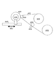
「本発明に用いられるa−Si感光体の算術平均粗さを調整する表面研磨装置」図4において、400はa−Si感光体、420は弾性支持機構、具体的には空気圧ホルダーで、本実施の形態ではブリジストン社製空気圧式ホルダー(商品名:エアーピック、型番:PO45TCA*820)を用いる。430は弾性支持機構420に対向して配置される加圧弾性ローラ、431は表面に研磨面を有し、加圧弾性ローラ430によって研磨面がa−Si感光体400に押圧される研磨テープ、432は研磨テープ431を加圧弾性ローラ430に送り出す送り出しロール、433は加圧弾性ローラ430から研磨テープ431を巻き取る巻き取りロール、434、435は研磨テープ431の移動を調整するための定量送り出しロール、キャプスタンローラである。弾性支持機構420は、基部440上に固定されており、基部440は位置調整手段441によって、弾性支持機構420と加圧弾性ローラ430との距離を自在に調整できる構成とされている。
【0079】
431の研磨テープは通常ラッピングテープと呼ばれるものが好ましく、表面に砥粒を担持する構成とされている。砥粒としてはSiC、Al2O3、Fe2O3などが好適に用いられる。ここでは、富士フィルム社製ラッピングテープLT−C2000を用いる。加圧弾性ローラ430は、ネオプレンゴム、シリコンゴムなど、適度な弾性を示す材質からなり、JISゴム硬度20〜80であり、JISゴム硬度30〜40が更に好適である。また形状は中央部の直径が両端部より太いものが好ましく、直径差が0〜0.6mm、更には0.2〜0.4mmが好適である。回転するa−Si感光体400に対して該ローラ430を0.5kg〜2.0kgに加圧(押圧)しながら、ラッピングテープを送りa−Si感光体400表面の研磨を行う。
【0080】
このように本発明に用いられるa−Si感光体の算術平均粗さは、前述したエッチングによる方法や、上記のような研磨装置による方法が好適に用いられるが、感光体の表面の算術平均粗さは、AFM(原子間力顕微鏡)、例えば、Quesant社製 Q−Scope250を用いて、測定、計算をすることができる。
【0081】
「本発明に用いられる接触帯電装置」
本発明に用いられる帯電手段は、導電性微粉体と、この導電性微粉体を表面に担持する帯電部材とを有し、該導電性微粉体がa−Si感光体と当接部を形成し、該帯電部材に電圧を印加することによってa−Si感光体を帯電させる接触式の帯電手段である。
【0082】
前記帯電部材は、a−Si感光体の表面に導電性微粉体を当接させることのできるように導電性微粉体を表面に担持することのできる導電性の部材であれば特に限定されず、好ましくは非磁性である芯金と、この芯金の周囲に設けられる樹脂製部材とによって構成される公知の形態を用いることができる。
【0083】
帯電部材は、多孔体表面を有する弾性体によって構成されることが、導電性微粉体を表面に担持する上で好ましい。また、帯電部材は、アスカーC硬度が50度以下のローラー部材であることが好ましく、より好ましくは25度以上50度以下である。硬度が低すぎると形状が安定しないために被帯電体との接触性が悪くなり、更に、帯電部材と感光体との当接部に導電性微粉体を介在させることでローラ部材表層を削り或いは傷つけ、安定した帯電性が得られないことがある。また、硬度が高すぎると被帯電体との間に帯電当接部を確保できないだけでなく、被帯電体表面へのミクロな接触性が悪くなることがある。
【0084】
また、弾性部材は、体積固有抵抗は1×10³Ω・cm以上1×10⁸Ω・cm以下のローラー部材であることが好ましい。帯電部材の体積固有抵抗が1×10³Ω・cmよりも小さいと、被帯電体にピンホールなどの欠陥部位が存在した場合に電圧のリークが発生することがあり、帯電部材の体積固有抵抗が1×10⁸Ω・cmよりも大きいと、被帯電体を十分に帯電することができない場合がある。
【0085】
上記のような帯電部材は、従来より知られている種々の樹脂化合物によって形成することができる。このような樹脂化合物としては、例えば、天然ゴム(加硫処理等)、エチレンプロピレンゴム(EPDM)、スチレンブタジエンゴム(SBR)、シリコーンゴム、ウレタンゴム、イソプレンゴム(IR)、ブチルゴム(BR)、ニトリルブタジエンゴム(NBR)、クロロプレンゴム(CR)等のゴム化合物や、ポリオレフィン系熱可塑性エラストマー、ウレタン系熱可塑性エラストマー、ポリスチレン系熱可塑性エラストマー、フッ素ゴム系熱可塑性エラストマー、ポリエステル系熱可塑性エラストマー、ポリアミド系熱可塑性エラストマー、ポリブタジエン系熱可塑性エラストマー、エチレン酢酸ビニル系熱可塑性エラストマー、ポリ塩化ビニル系熱可塑性エラストマー及び塩素化ポリエチレン系熱可塑性エラストマー等の熱可塑性エラストマー等を例示することができる。これらの材料は、単独または二種類以上を混合しても良く、共重合体であっても良い。
【0086】
これらの樹脂化合物によって形成される帯電部材には、例えば導電性粒子を部材中に分散させること等により、適切な導電性を与えることができる。このような導電性粒子としては、例えば、カーボンブラック、導電性金属酸化物、アルカリ金属塩及びアンモニウム塩等を例示することができる。
【0087】
また、上記のような樹脂化合物によって帯電部材を形成する場合で、帯電部材を多孔体表面の弾性体とする場合では、公知の技術を利用することができ、このような手段としては、例えば、弾性部材の発泡成形等を例示することができる。また、帯電部材の硬度は、上記の発泡成形や、軟化油、可塑剤等の添加等の公知技術を利用して調整することができる。
【0088】
帯電部材の硬度は、高分子計器(株)製のAsker−Cゴム硬度計を用いて測定することができる。より詳しくは、本硬度計により、帯電部材の任意の五点におけるゴム硬度を測定し、その五点の平均値をもって、帯電部材の硬度とする。
【0089】
帯電部材の体積固有抵抗は、例えば抵抗測定装置(三菱化学(株)製絶縁抵抗計Hiresta−UP)を用いて測定することができる。より詳しくは、帯電部材材料自体を2mm厚に膜成形し、23℃、55%の環境で10Vの電圧を1分間印加して導電性の測定を行う。測定に際しては、帯電部材を形成するのと同一の弾性組成物を塗料化し、そのクリア塗料をアルミシート上にコーティングし、上記の条件で帯電部材の導電性を測定する。
【0090】
前記導電性微粉体は、抵抗が1×10⁹Ω・cm以下であることが好ましい。導電性微粉体の抵抗が1×10⁹Ω・cmよりも大きいと、導電性微粉体を帯電部材と電子写真感光体との当接部またはその近傍の帯電領域に介在させ、接触帯電部材の導電性微粉体を介しての電子写真感光体への緻密な接触性を維持させても、良好な帯電性を得るための帯電促進効果が得られないことがある。また、導電性微粉体の抵抗が1×10⁻¹Ω・cm以上であることが、該微粉体が帯電し非画像部に現像され帯電を促進するために好ましい。
【0091】
また、導電性微粉体は、体積平均粒子径が0.5〜10μmであることが好ましい。導電性微粉体の平均粒子径が0.5μmよりも小さいと、現像性の低下を防ぐために導電性微粉体のトナー全体に対する含有量を小さく設定しなければならない場合があり、この観点から、導電性微粉体の平均粒子径は好ましくは0.8μm以上、更に好ましくは1.1μm以上が良い。また、導電性微粉体の平均粒子径が10μmよりも大きいと、帯電部材から脱落した導電性微粉体は静電潜像を書き込む露光光を遮光または拡散し、静電潜像の欠陥を生じ画像品位を低下させる場合がある。
【0092】
また、導電性微粉体は、透明、白色または淡色の導電性微粉体であることが、転写材上に転写される導電性微粉体がカブリとして目立たないため好ましく良い。また、潜像形成工程における露光光の妨げとならない意味でも導電性微粉体は、透明、白色または淡色の導電性微粉体であることがよく、より好ましくは、導電性微粉体の露光光に対する透過率が30%以上であることが良い。
【0093】
上記導電性微粉体の材料としては、例えばカーボンブラック、グラファイトなどの炭素微粉末;銅、金、銀、アルミニウム、ニッケルなどの金属微粉末;酸化亜鉛、酸化チタン、酸化すず、酸化アルミニウム、酸化インジウム、酸化珪素、酸化マグネシウム、酸化バリウム、酸化モリブデン、酸化鉄、酸化タングステンなどの金属酸化物;硫化モリブデン、硫化カドミウム、チタン酸カリなどの金属化合物、またはこれらの複合酸化物などが必要に応じて粒度及び粒度分布を調整することで使用できる。これらの中でも酸化亜鉛、酸化すず、酸化チタン等の無機酸化物微粒子が特に好ましい。
【0094】
また、導電性無機酸化物の抵抗値を制御する等の目的で、アンチモン、アルミニウムなどの元素をドープした金属酸化物、導電性材料を表面に有する微粒子なども使用できる。このような微粒子としては、例えば酸化スズ・アンチモンで表面処理された酸化チタン微粒子、アンチモンでドープされた酸化第二スズ微粒子、または酸化第二スズ微粒子などを例示することができる。
【0095】
導電性微粉体の抵抗は、例えば錠剤法によって測定することができる。錠剤法による測定では、まずセルに導電性微粉体を充填し、充填された導電性微粉体に接するよう上下に電極を配し、電極間に電圧を印加し、その時流れる電流量から導電性微粉体の抵抗を算出することができる。なお、この場合の測定条件としては、温度23℃、湿度65%の環境中で、充填された導電性微粉体と電極との接触面積は2cm2、導電性微粉体の充填厚みは1mm、上部電極にかける加重は10kg、印加電圧は100Vである。
【0096】
本発明における導電性微粉体の体積平均粒径及び粒度分布は、コールター社製、LS−230型レーザ回折式粒度分布測定装置にリキッドモジュールを取付けて0.04〜2000μmの測定範囲で測定することにより実施できる。測定方法としては、純水10mLに微量の界面活性剤を添加し、これに導電性微粉体の試料10mgを加え、超音波分散機(超音波ホモジナイザー)にて10分間分散した後、測定時間90秒、測定回数1回で測定する方法が挙げられる。
【0097】
本発明に用いられる帯電手段は、前述した帯電部材及び導電性微粉体の他にも、導電性微粉体を収容し、帯電部材表面に導電性微粉体を供給する導電性微粉体補給手段を更に有することができる。このような補給手段としては、例えば帯電部材に面して開口する容器体等を挙げることができる。またこの容器体内には収容されている導電性微粉体を撹拌、搬送するための撹拌搬送手段(例えば回転翼やコンベア等)を設けても良い。
【0098】
前述したような帯電手段は、当接部において、帯電部材の表面がa−Si感光体の表面に対して相対的速度差を有して移動しながらa−Si感光体を帯電することが、感光体を均一に帯電する上で好ましい。さらに帯電手段は前記当接部において、帯電部材とa−Si感光体とが互いに逆方向に移動しつつa−Si感光体を帯電することが、同様の理由からより一層好ましい。
以下、本発明に用いられる帯電手段について、その一例を図示し説明する。
【0099】
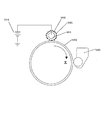
図5は、接触帯電器として粒子を介在させた弾性ローラーを用いた場合の画像形成装置の模式図である。粒子を介在させた弾性ローラー帯電器は、導電部材からなる芯金501の上に、スポンジローラーなどの多孔体表面を有し、かつ導電性を有する弾性体である帯電部材502を設け、さらにその表面に導電性を有する導電性微粉体505を付着させた帯電手段である。この帯電手段は、弾性体の帯電部材502と感光体503の間に導電性微粉体505が介在することにより、接触状態を向上させ、帯電電荷の注入性を改善した帯電装置である。
【0100】
芯金501には電圧印加手段504が接続され、直流電圧Vdcが芯金501を経由し、帯電部材502に印加されて、感光体503の表面との接触部位の間に介在した導電性微粉体505を介して感光体503へ電荷を直接注入し、均一に帯電させる。粒子を介在させた弾性ローラー帯電器は感光体503の回転方向Xに対して適宜な相対速度で回転、移動する。弾性ローラー帯電器は感光体503に対して振動していても良い。
【0101】
なお、この模式図では、クリーナーレスの画像形成装置を示している。帯電、露光により形成された潜像は、現像器506で顕像化され、不図示の転写手段で転写材に転写される。その際に感光体上に残留した転写残トナーは導電性微粉体505を介在させた弾性ローラー帯電器で帯電された後、現像器506に再び到達し、そこで現像器506内からの新規の現像剤による現像と、感光体上を搬送されてきた転写残トナーの回収が同時に行われる。この模式図では、帯電部材502と感光体503の間に介在する導電性微粉体505はトナーに外添され、感光体503表面に残留した導電性微粉体505が帯電器に到達し、導電性微粉体505の帯電器への補給が行われる形態を示している。
【0102】
図6は図5と同様の帯電装置に、更に導電性微粉体605を供給する導電性微粉体補給手段607を帯電部材602上部に設けている。その他の構成については、図5の帯電装置と同様である。
【0103】
「本発明に用いられるトナー」
本発明に用いられるトナーは、平均円形度が0.950乃至1.000であり、より好ましくは0.950乃至0.995である。このような平均円形度のトナーは、感光体との接触面積が小さく、鏡像力やファンデルワールス力等に起因するトナーの感光体への付着力が低下すると考えられており、優れた転写性と優れた離型性を示し、高画質の画像形成を達成することができ、かつ現像兼クリーニング方式において、感光体と現像器との間におけるトナーの円滑な授受を達成することができる。また、上記平均円形度のトナーは、表面にエッジ部がほとんどないことから、感光体表面を引っ掻くことによる感光体削れを防止するのに好適である。本発明に用いられるトナーの平均円形度が0.950よりも小さいと、上記のような効果が十分に得られないことがある。
【0104】
また、本発明に用いられるトナーは、79.6kA/m(1000エルステッド)における飽和磁化が10Am2/kg(emu/g)以上50Am2/kg以下である。現像器内におけるトナーの搬送は、一般に磁界発生手段を内包する回転自在な非磁性円筒(現像スリーブ)によって担持搬送されるが、上記飽和磁化のトナーは、現像器内での良好な搬送性と撹拌性、感光体へのトナーの供給にあたり現像スリーブ表面で穂立ちを形成するトナーの飛散防止、及び感光体からの良好な回収性を達成することができる。
【0105】
本発明に用いられるトナーの上記飽和磁化が10Am2/kgよりも小さいと、上記の効果が十分に得られず、現像器内におけるトナーの搬送が不十分であったり、また、カブリ、画像濃度ムラ、及び転写残トナーの回収不良に起因する画像不良等を生じることがある。上記飽和磁化が50Am2/kgよりも大きいと、トナーの磁気凝集によってトナーの流動性が低下し、また、転写性が低下することによる転写性の低下、及び転写残トナーの増加を生じることがある。
【0106】
なお、本発明において、トナーの飽和磁化を磁場79.6kA/mで規定するが、画像形成装置に磁性トナーが適用される場合、磁性トナーに作用する磁場は、画像形成装置外への磁場の漏洩を大きくしないため、または磁場発生源のコストを低く抑えるために、市販されている多くの画像形成装置において数十から百数十kA/mとされている。そこで、本発明では、画像形成装置内で実際に磁性トナーに作用する磁場の代表的な値として磁場79.6kA/m(1000エルステッド)を選択し、磁場79.6kA/mにおけるトナーの飽和磁化を規定した。
【0107】
本発明に用いられるトナーは、少なくとも結着樹脂と磁性体とを含有するトナー粒子と、無機微粉体とを有するトナーであり、かつ上記条件を満たすトナーであれば特に限定されない。また、本発明に用いられるトナーは、結着樹脂及び磁性体の他にも、良好な物性を示す他の好ましい材料や、製造過程において好適に利用される他の材料をさらに使用することができる。
【0108】
本発明に用いられるトナーは、上記条件を満足するものであれば特にその製造方法は限定されず、従来より知られている種々の製造方法を利用することができる。このようなトナーの製造方法としては、例えば、粉砕法や重合法等を例示することができる。
【0109】
上記トナー粒子を粉砕法で製造する場合では、公知の方法を用いることができ、例えば結着樹脂、磁性体、及び離型剤、可塑剤、荷電制御剤、着色剤等、トナーとして必要な成分及びその他の添加剤等をヘンシェルミキサー、ボールミル等の混合器により十分に混合し、加熱ロール、ニーダー、エクストルーダの如き熱混練機を用いて熔融混練して樹脂類をお互いに相熔せしめ、磁性体等の他のトナー材料を分散または溶解せしめ、冷却固化、粉砕後、分級し、必要に応じて表面処理を行うことによりトナー粒子を得ることが出来る。分級及び表面処理の順序はどちらが先でもよい。分級工程においては生産効率上、多分割分級機を用いることが好ましい。
【0110】
粉砕工程は、機械衝撃式、ジェット式等の公知の粉砕装置を用いた方法により行うことができる。本発明に係わる特定の円形度を有するトナー粒子を得るためには、さらに熱をかけて粉砕したり、または補助的に機械的衝撃を加える処理をすることが好ましい。また、微粉砕(必要に応じて分級)されたトナー粒子を熱水中に分散させる湯浴法、熱気流中を通過させる方法などを用いても良い。
【0111】
機械的衝撃力を加える手段としては、例えば川崎重工社製のクリプトロンシステムやターボ工業社製のターボミル等の機械衝撃式粉砕機を用いる方法、また、ホソカワミクロン社製のメカノフージョンシステムや奈良機械製作所製のハイブリダイゼーションシステム等の装置のように、高速回転する羽根によりトナー粒子をケーシングの内側に遠心力により押しつけ、圧縮力、摩擦力等の力によりトナー粒子に機械的衝撃力を加える方法が挙げられる。
【0112】
機械的衝撃法を用いる場合においては、処理温度をトナー粒子のガラス転移点Tg付近の温度(Tg±10℃)を加える熱機械的衝撃が、凝集防止、生産性の観点から好ましい。さらに好ましくは、トナー粒子のガラス転移点Tg±5℃の範囲の温度で行うことが、転写効率を向上させるのに特に有効である。
【0113】
上記トナー粒子は、上述した粉砕法によっても製造することができるが、この粉砕法で得られるトナー粒子は一般に不定形のものであり、本発明に用いられるトナーの必須要件である平均円形度が0.950以上という物性という好ましい物性を得るためには機械的・熱的または何らかの特殊な処理を行うことが必要となる。そこで、本発明においては、トナーを懸濁重合法によって製造することがより好ましい。上記トナー粒子を重合法で製造する場合では、公知の方法を用いることができ、例えば重合性単量体、磁性体、及び離型剤、可塑剤、荷電制御剤、架橋剤、着色剤等、トナーとして必要な成分及びその他の添加剤、例えば重合反応で生成する重合体の粘度を低下させるために入れる有機溶媒、高分子重合体、分散剤等を適宜加えて、ホモジナイザー、ボールミル、コロイドミル、超音波分散機等の分散機に依って均一に溶解または分散せしめた単量体系を、分散安定剤を含有する水系媒体中に懸濁し、その状態で重合させることにより得ることができる。
【0114】
懸濁時においては、高速撹拌機もしくは超音波分散機のような高速分散機を使用して一気に所望のトナー粒子のサイズとする方が、得られるトナー粒子の粒径がシャープになる。重合開始剤添加の時期としては、単量体系の重合前における任意の段階で添加することができ、重合性単量体中に他の添加剤を添加する時同時に加えても良いし、水系媒体中に懸濁する直前に混合しても良い。又、造粒直後、重合反応を開始する前に重合性単量体または溶媒に溶解した重合開始剤を加える事も出来る。単量体系の重合によって造粒がなされた後は、通常の攪拌機を用いて、粒子状態が維持され、かつ粒子の浮遊・沈降が防止される程度の撹拌を行えば良い。
【0115】
本発明の画像形成方法に関わる重合トナーを製造する場合には、分散安定剤として公知の界面活性剤や有機・無機分散剤が使用でき、中でも無機分散剤が有害な超微粉を生じ難く、その立体障害性により分散安定性を得ているので反応温度を変化させても安定性が崩れ難く、洗浄も容易でトナーに悪影響を与え難いので、好ましく使用できる。
【0116】
前記重合工程においては、重合温度は40℃以上、一般には50〜90℃の温度に設定して重合を行う。この温度範囲で重合を行うと、内部に封じられるべき離型剤やワックスの類が、相分離により析出して内包化がより完全となる。残存する重合性単量体を消費するために、重合反応終期ならば、反応温度を90〜150℃にまで上げることは可能である。
【0117】
さらにまた、本発明に用いられるトナーは、単量体には可溶で得られる重合体が不溶な水系有機溶剤を用い直接トナーを生成する分散重合方法又は水溶性極性重合開始剤存在下で直接重合しトナーを生成するソープフリー重合方法に代表される乳化重合方法等を用いトナーを製造する方法、乳化重合で得られたポリマー粒子等を会合凝集させる方法でも製造が可能である。
【0118】
上記のような重合トナー粒子は重合終了後、公知の方法によって濾過、洗浄、乾燥を行い、無機微粉体を混合し表面に付着させることで、トナーを得ることができる。また、製造工程に分級工程を入れ、粗粉や微粉をカットすることも、本発明の望ましい形態の一つである。また、分級工程によれば、所定の粒径に分類されたトナー粒子を混合することによって、所望の粒度分布を有するトナー粒子を調製することもできる。
【0119】
上記トナー粒子には、従来より知られている種々の結着樹脂が用いられる。このような結着樹脂としては、例えば、ポリスチレン、ポリビニルトルエンなどのスチレン及びその置換体の単重合体;スチレン−プロピレン共重合体、スチレン−ビニルトルエン共重合体、スチレン−ビニルナフタリン共重合体、スチレン−アクリル酸メチル共重合体、スチレン−アクリル酸エチル共重合体、スチレン−アクリル酸ブチル共重合体、スチレン−アクリル酸オクチル共重合体、スチレン−アクリル酸ジメチルアミノエチル共重合体、スチレン−メタアクリル酸メチル共重合体、スチレン−メタアクリル酸エチル共重合体、スチレン−メタアクリル酸ブチル共重合体、スチレン−メタクリル酸ジメチルアミノエチル共重合体、スチレン−ビニルメチルエーテル共重合体、スチレン−ビニルエチルエーテル共重合体、スチレン−ビニルメチルケトン共重合体、スチレン−ブタジエン共重合体、スチレン−イソプレン共重合体、スチレン−マレイン酸共重合体、スチレン−マレイン酸エステル共重合体などのスチレン系共重合体;ポリメチルメタクリレート、ポリブチルメタクリレート、ポリ酢酸ビニル、ポリエチレン、ポリプロピレン、ポリビニルブチラール、シリコン樹脂、ポリエステル樹脂、ポリアミド樹脂、エポキシ樹脂、ポリアクリル酸樹脂、ロジン、変性ロジン、テルペン樹脂、フェノール樹脂、脂肪族または脂環族炭化水素樹脂、芳香族系石油樹脂等を例示することができ、これらを一種または二種以上を用いることができる。
【0120】
また、上記トナー粒子には、従来より知られている種々の磁性体が用いられる。このような磁性体としては、例えば、四三酸化鉄、γ−酸化鉄等、酸化鉄等を主成分とするものを例示することができ、これらを一種または二種以上を用いることができる。磁性体には、さらにリン、コバルト、ニッケル、銅、マグネシウム、マンガン、アルミニウム、珪素等の他の元素を含んでも良い。これら磁性体は、窒素吸着法によるBET比表面積が好ましくは2〜30m2/g、特に好ましくは3〜28m2/gであり、更にモース硬度が5〜7のものが好ましい。磁性体は、前述したトナーの飽和磁化を満たすように、その種類や配合量について、適切に選択することが好ましい。
【0121】
上記磁性体は、疎水化処理されていることが好ましく、疎水化処理には、水系媒体中で加水分解しながら磁性体の表面に結合するシランカップリング剤やチタンカップリング剤等のカップリング剤が好適に用いられる。この中でもシランカップリング剤が好ましく、このようなシランカップリング剤としては、例えば、ビニルトリメトキシシラン、ビニルトリエトキシシラン、γ−メタクリルオキシプロピルトリメトキシシラン、ビニルトリアセトキシシラン、メチルトリメトキシシラン、メチルトリエトキシシラン、イソブチルトリメトキシシラン、ジメチルジメトキシシラン、ジメチルジエトキシシラン、トリメチルメトキシシラン、ヒドロキシプロピリトリメトキシシラン、フェニルトリメトキシシラン、n−ヘキサデシルトリメトキシシラン、n−オクタデシルトリメトキシシラン等を例示することができ、これらを一種または二種以上を用いることができる。
【0122】
また、上記トナー粒子には、従来より知られている種々のワックス類を離型剤または可塑剤として用いることができる。このようなワックスとしては、例えば、パラフィンワックス、マイクロクリスタリンワックス、ペトロラクタム等の石油系ワックス及びその誘導体、モンタンワックス及びその誘導体、フィッシャートロプシュ法による炭化水素ワックス及びその誘導体、ポリエチレンに代表されるポリオレフィンワックス及びその誘導体、カルナバワックス、キャンデリラワックス等天然ワックス及びその誘導体などで、誘導体には酸化物や、ビニル系モノマーとのブロック共重合物、グラフト変性物を含む。さらには、高級脂肪族アルコール、ステアリン酸、パルミチン酸等の脂肪酸、またはその化合物、酸アミドワックス、エステルワックス、ケトン、硬化ヒマシ油及びその誘導体、植物系ワックス、動物性ワックス等を例示することができ、これらを一種または二種以上を用いることができる。
【0123】
上記ワックスは、示差熱分析における吸熱ピークが比較的低温にあると可塑性が発揮され、低温定着性に優れるトナーが製造され、示差熱分析における吸熱ピークが比較的高い温度にあると離型性が発揮され、画像耐久性に優れるトナーが製造される。従って使用するワックス類の種類及び配合量の選択については、これらの特性を考慮して適切に選択することが望まれる。
【0124】
また、上記トナー粒子には、従来より知られている種々の着色剤が用いられる。このような着色剤としては、磁性または非磁性無機化合物、公知の染料及び顔料等、より具体的には、例えば、コバルト、ニッケルなどの強磁性金属粒子、またはこれらにクロム、マンガン、銅、亜鉛、アルミニウム、希土類元素などを加えた合金、ヘマタイトなどの粒子、チタンブラック、ニグロシン染料/顔料、カーボンブラック、フタロシアニン等を例示することができ、これらを一種または二種以上用いることができる。これらの着色剤もまた、磁性粉体と同様に表面を疎水処理して用いても良い。
【0125】
また、上記トナー粒子には、従来より知られている種々の荷電制御剤が用いられる。このような荷電制御剤としては、例えば、ネガ系荷電制御剤としてサリチル酸、アルキルサリチル酸、ジアルキルサリチル酸、ナフトエ酸、ダイカルボン酸の如き芳香族カルボン酸の金属化合物、アゾ染料あるいはアゾ顔料の金属塩または金属錯体、スルホン酸またはカルボン酸基を側鎖に持つ高分子型化合物、ホウ素化合物、尿素化合物、ケイ素化合物、カリックスアレーン等をネガ系荷電制御剤として例示することができ、これらを一種または二種以上用いることができる。また、荷電制御剤としては、例えば、四級アンモニウム塩、該四級アンモニウム塩を側鎖に有する高分子型化合物、グアニジン化合物、ニグロシン系化合物、イミダゾール化合物等をポジ系荷電制御剤として例示することができ。これらを一種または二種以上用いることができる。
【0126】
前記重合性単量体としては、従来より知られている種々の重合性単量体を使用することができ、例えば、スチレン、o−メチルスチレン、m−メチルスチレン、p−メチルスチレン、p−メトキシスチレン、p−エチルスチレン等のスチレン系単量体、アクリル酸メチル、アクリル酸エチル、アクリル酸n−ブチル、アクリル酸イソブチル、アクリル酸n−プロピル、アクリル酸n−オクチル、アクリル酸ドデシル、アクリル酸2−エチルヘキシル、アクリル酸ステアリル、アクリル酸2−クロルエチル、アクリル酸フェニル等のアクリル酸エステル類、メタクリル酸メチル、メタクリル酸エチル、メタクリル酸n−プロピル、メタクリル酸n−ブチル、メタクリル酸イソブチル、メタクリル酸n−オクチル、メタクリル酸ドデシル、メタクリル酸2−エチルヘキシル、メタクリル酸ステアリル、メタクリル酸フェニル、メタクリル酸ジメチルアミノエチル、メタクリル酸ジエチルアミノエチル等のメタクリル酸エステル類、その他のアクリロニトリル、メタクリロニトリル、アクリルアミド等の単量体を例示することができ、これらの一種または二種以上を用いることができる。上述の単量体の中でも、スチレンまたはスチレン誘導体を少なくとも含むように上記単量体を使用することが、得られる磁性トナーの現像特性及び耐久性の点から好ましい。
【0127】
重合法でトナー粒子を製造する場合では、重合性単量体に比して極性の高い樹脂化合物を単量体中に含ませることが好ましい。このような樹脂化合物を混合することにより、磁性体やワックス類等の内包化が強くなり、耐オフセット性、耐ブロッキング性、低温安定性等が向上する。このような樹脂化合物としては、例えば、アミノ基やカルボン酸基、水酸基等の親水基を有する重合体やポリエステル樹脂等を例示することができ、これらを一種または二種以上用いることができる。
【0128】
また、前記重合開始剤としては、従来より知られている種々の重合開始剤を使用することができ、例えば、2,2'−アゾビス−(2,4−ジメチルバレロニトリル)、2,2'−アゾビスイソブチロニトリル、1,1'−アゾビス(シクロヘキサン−1−カルボニトリル)、2,2'−アゾビス−4−メトキシ−2,4−ジメチルバレロニトリル、アゾビスイソブチロニトリル等のアゾ系またはジアゾ系重合開始剤、ベンゾイルパーオキサイド、メチルエチルケトンパーオキサイド、ジイソプロピルパーオキシカーボネート、クメンヒドロパーオキサイド、2,4−ジクロロベンゾイルパーオキサイド、ラウロイルパーオキサイド、t−ブチルパーオキシ−2−エチルヘキサノエート等の過酸化物系重合開始剤等を例示することができ、これらを一種または二種以上用いることができる。
【0129】
また、前記架橋剤としては、主として二個以上の重合可能な二重結合を有する化合物で従来より知られている種々の架橋剤を使用することができ、例えば、ジビニルベンゼン、ジビニルナフタレン等のような芳香族ジビニル化合物;例えばエチレングリコールジアクリレート、エチレングリコールジメタクリレート、1,3−ブタンジオールジメタクリレート等のような二重結合を二個有するカルボン酸エステル;ジビニルアニリン、ジビニルエーテル、ジビニルスルフィド、ジビニルスルホン等のジビニル化合物;及び三個以上のビニル基を有する化合物等を例示することができ、これらを一種または二種以上用いることができる。
【0130】
また、前記分散安定剤として、従来より知られている種々の界面活性剤、有機分散剤、無機分散剤等の分散安定剤を使用することができる。
上記界面活性剤としては、例えば、ドデシルベンゼン硫酸ナトリウム、テトラデシル硫酸ナトリウム、ペンタデシル硫酸ナトリウム、オクチル硫酸ナトリウム、オレイン酸ナトリウム、ラウリル酸ナトリウム、ステアリン酸ナトリウム、ステアリン酸カリウム等を例示することができ、これらを一種または二種以上用いることができる。
【0131】
上記有機分散剤としては、例えば、ポリビニルアルコール、ゼラチン、メチルセルロース、メチルヒドロキシプロピルセルロール、エチルセルロース、カルボキシメチルセルロースのナトリウム塩、ポリアクリル酸及びその塩、デンプン等を例示することができ、これらを一種または二種以上用いることができる。
【0132】
上記無機分散剤としては、例えば、燐酸カルシウム、燐酸マグネシウム、燐酸アルミニウム、燐酸亜鉛等の燐酸多価金属塩、炭酸カルシウム、炭酸マグネシウム等の炭酸塩、メタ硅酸カルシウム、硫酸カルシウム、硫酸バリウム等の無機塩、水酸化カルシウム、水酸化マグネシウム、水酸化アルミニウム、シリカ、ベントナイト、アルミナ等の無機酸化物等を例示することができ、これらを一種または二種以上用いることができる。
【0133】
本発明のトナーは、前述のように製造されたトナー粒子に少なくとも無機微粉体を外添することにより構成される。この無機微粉体は、トナー粒子の流動性や帯電性を向上させることを目的として添加される。
【0134】
上記無機微粉体は、従来より知られている種々の無機微粉体を使用することができる。このような無機微粉体としては、例えば、シリカ、アルミナ、チタニアなどを例示することができ、これらを一種または二種以上用いることができる。より詳しくは、例えば、ケイ酸微粉体としてはケイ素ハロゲン化物の蒸気相酸化により生成されたいわゆる乾式法又はヒュームドシリカと称される乾式シリカ、及び水ガラス等から製造されるいわゆる湿式シリカの両者が使用可能であるが、表面及びシリカ微粉体の内部にあるシラノール基が少なく、またNa2O、SO3 2-等の製造残滓の少ない乾式シリカの方が好ましい。また乾式シリカにおいては、製造工程において例えば、塩化アルミニウム、塩化チタン等他の金属ハロゲン化合物をケイ素ハロゲン化合物と共に用いることによって、シリカと他の金属酸化物の複合微粉体(複酸化物)を得ることも可能であり、前記無機微粉体はそれらも包含するものである。
【0135】
また、上記無機微粉体は、トナー全量に対して総量で0.1〜3.0質量%配合されることが好ましい。無機微粉体の配合量が0.1質量%よりも小さいと、無機微粉体の外添による効果(トナーの流動性や帯電性の向上等)が十分に発揮されないことがある。また、無機微粉体の配合量が3.0質量%よりも大きいと、定着性が悪くなることがある。
【0136】
また、上記無機微粉体は、表面が疎水化処理されていることが好ましい。このような疎水化処理に使用される処理剤としては公知の処理剤を使用することができ、特に限定されないが、例えば、シランカップリング剤やチタンカップリング剤等のカップリング剤による疎水化処理を例示することができる。
【0137】
また、上記無機微粉体は、シリコーンオイルで疎水化処理されていることがより好ましい。このような疎水化処理に使用されるシリコーンオイルとしては、例えば、ジメチルシリコーンオイル、メチルフェニルシリコーンオイル、α−メチルスチレン変性シリコーンオイル、クロルフェニルシリコーンオイル、フッ素変性シリコーンオイル等を例示することができ、これらを一種または二種以上用いることができる。
【0138】
本発明に用いられるトナーの平均円形度は、粒子の形状を定量的に表現する簡便な方法として用いたものであり、本発明では東亜医用電子製フロー式粒子像分析装置「FPIA−1000」を用いて測定を行い、3μm以上の円相当径の粒子群について測定された各粒子の円形度(Ci)を下式(1)によりそれぞれ求め、さらに下式(2)で示すように測定された全粒子の円形度の総和を全粒子数(m)で除した値を平均円形度(Ca)と定義する。
【0139】
【数4】
なお、本発明で用いている測定装置である「FPIA−1000」は、各粒子の円形度を算出後、平均円形度の算出に当たって、粒子を得られた円形度によって、円形度0.40〜1.00を61分割したクラスに分け、分割点の中心値と頻度を用いて平均円形度の算出を行う算出法を用いている。しかしながら、この算出法で算出される平均円形度の値と、上述した各粒子の円形度を直接用いる算出式によって算出される平均円形度の値との誤差は、非常に少なく、実質的には無視出来る程度のものであり、本発明においては、算出時間の短絡化や算出演算式の簡略化の如きデータの取り扱い上の理由で、上述した各粒子の円形度を直接用いる算出式の概念を利用し、一部変更したこのような算出法を用いても良い。
【0141】
具体的な測定方法としては、界面活性剤を約0.1mg溶解している水10mLに現像剤約5mgを分散させて分散液を調整し、超音波(20kHz、50W)を分散液に5分間照射し、分散液濃度を5000〜2万個/μLとして、前記装置により測定を行い、3μm以上の円相当径の粒子群の平均円形度を求める。
【0142】
本発明における平均円形度とは、現像剤の凹凸の度合いの指標であり、現像剤が完全な球形の場合1.000を示し、現像剤の表面形状が複雑になるほど平均円形度は小さな値となる。
【0143】
なお、本測定において3μm以上の円相当径の粒子群についてのみ円形度を測定する理由は、3μm未満の円相当径の粒子群にはトナー粒子とは独立して存在する外部添加剤の粒子群も多数含まれるため、その影響によりトナー粒子群についての円形度が正確に見積もれないからである。
【0144】
本発明において磁性トナーの磁化の強さは、振動型磁力計VSM P−1−10(東英工業社製)を用いて、25℃の室温にて外部磁場79.6kA/mで測定した。
【0145】
「本発明の画像形成装置及び画像形成方法」
本発明の画像形成装置は、前述したa−Si感光体及び帯電手段と、像露光を行うことによりa−Si感光体上に静電潜像を形成する潜像形成手段と、静電潜像をa−Si感光体上で前記トナーによって可視化する現像手段と、可視化像を転写材に転写する転写手段とを有する。
【0146】
前記潜像形成手段は、特に限定されず、従来より知られている種々の潜像形成手段を用いることができる。このような潜像形成手段としては、例えば、レーザー光を利用するものや、LEDを利用するもの等を例示することができる。
【0147】
前記現像手段は、a−Si感光体に前記トナーを供給することのできる現像手段であれば良く、公知の現像手段を用いることができる。現像手段は、a−Si感光体へのトナーの供給のみならず、可視化像を転写材上に転写した後にa−Si感光体上に残留したトナーを回収するクリーニング手段を兼ねる現像手段であると、独立したクリーニング手段を画像形成装置に設ける必要がないことから、画像形成装置の小型化を達成することができる。また、クリーニング手段を兼ねる現像手段であると、トナーの再利用が達成されることから、エコロジーの観点からも好ましい。
【0148】
クリーニング手段を兼ねる現像手段は、現像手段とa−Si感光体との対向部である現像部における電位差を利用してトナーを授受する構成とすることにより実現できる。このような現像手段としては、例えば、トナーを収容する現像容器と、現像容器の開口部に回転自在に設けられ内部に磁界発生手段を有する非磁性かつ導電性の現像スリーブと、現像スリーブ上に担持されるトナーの層圧を規制する現像ブレードと、現像スリーブに現像バイアスを印加する電源とを有する現像手段を例示することができる。
【0149】
また、本発明に用いられる現像手段は、上記のようにクリーニング手段を兼ねるだけでなく、前記導電性微粉体の供給手段としての機能を兼ねることができる。すなわち、現像手段に導電性微粉体とトナーとを収容し、導電性微粉体がトナーの表面に付着している状態にする。そして、a−Si感光体へのトナーの供給に伴い導電性微粉体をa−Si感光体に供給する。
【0150】
a−Si感光体に供給されたトナー及び導電性微粉体は、転写手段との対向部である転写ニップ部に搬送されるが、転写ニップ部ではトナーのみが転写材へ移行し、導電性微粉体はa−Si感光体上に残留する。従って、導電性微粉体はそのまま感光体によって帯電手段まで搬送され、前述した帯電部材の表面に担持される。このように、現像手段に導電性微粉体とトナーとをともに収容することにより、導電性微粉体の供給手段を兼ねる現像手段とすることができる。
【0151】
前記転写手段は、静電潜像に対向してa−Si感光体上に付着したトナーを転写材に転写することのできる転写手段であれば特に限定されず、公知の転写手段を用いることができる。このような転写手段としては、例えば、転写バイアスを印加することにより、現像に供されたトナーを静電的にa−Si感光体上から転写材上へ移行させる転写手段等を例示することができる。
【0152】
本発明の画像形成方法は、前述したa−Si感光体を前記帯電手段により接触帯電し、帯電されたa−Si感光体上に静電潜像を形成し、前記トナーによって該静電潜像を可視化することを特徴とする画像形成方法である。本発明の画像形成方法は、上記のような帯電工程及び現像工程が行われる方法であれば良く、その後の転写工程や定着工程等については特に限定されず、公知の技術を利用することができる。
以下、本発明の画像形成装置及び画像形成方法について、その一例を図示し説明する。
【0153】
図7は本発明の画像形成装置及び画像プロセスの一例を示す概略図であって、電子写真感光体701は最表面の算術平均粗さRaが100nm以下のa−C:H表面層を有するa−Si感光体であり、矢印方向Xに回転する。電子写真感光体701の周辺には、本発明によるところの導電性微粉体を表面に付着させた弾性ローラー帯電器702、静電潜像形成部位703、現像器704、転写紙供給系705、転写ローラー706、クリーニングローラー707、搬送系708、除電光源709等が配設されている。
【0154】
以下、さらに具体的に画像形成プロセスを説明すると、電子写真感光体701はマイナスのDC電圧を印加した粒子を介在させた弾性ローラー帯電器702により一様に帯電される。これに、スキャナーで読み込んだ画像情報やコンピューターから入力された画像情報によって駆動される半導体レーザー710から発されたレーザー光がポリゴンミラー713で反射し、レンズユニット717のレンズ718によって結像され、ミラー716を経由し、電子写真感光体701上に導かれて投影され、静電潜像が形成される。この潜像に現像器704からネガ極性トナーが供給されてトナー像が形成される。
【0155】
一方、転写紙供給系705を通って、レジストローラー722によって先端タイミングを調整され、電子写真感光体701方向に供給される転写材Pは高電圧を印加した転写ローラー706と電子写真感光体701の間隙において背面から、トナーとは逆極性の電界を与えられ、これによって電子写真感光体表面のトナー像は転写材Pに転写する。次いで、転写材Pは転写搬送系708を通って定着装置724に至り、トナー像が定着されて装置外に搬出される。
【0156】
電子写真感光体701上に残留するトナーは弾性ローラー帯電器702を経由した後、現像器704によって回収される。残留する静電潜像は除電光源709によって消去される。
【0157】
【実施例】
以下、実施例により本発明の効果を具体的に説明する。なお、本発明はこれらの実施例に限定されるものではない。また、本実施例で「部」とは質量部である。
【0158】
<実施例1>
図2に示すRFプラズマCVD法によるa−Si感光体の製造装置を用い、鏡面加工を施したアルミニウムシリンダー上に、表1に示す条件で電荷注入阻止層、光導電層、バッファ層を積層した。さらにその上に表2の作製条件でa−C:Hからなる表面層を積層することでマイナス帯電で用いられる感光体を合計6本作製した。なお、RFの周波数は13.56MHzを用いた。
同時に、表2の作製条件によって表面層のサンプルをSiウェハー上に製膜し、赤外分光光度計により赤外吸収スペクトルを測定した。そして2920cm-1付近に現れるC−Hnの吸収ピークの面積と膜厚から膜中水素量を求めた。その結果、炭素膜全量に対する水素量[H/(C+H)]は45原子%であった。
こうして得られた感光体に対して、図4に示した表面研磨装置を用いて、算術平均粗さRaを5nm〜100nmに変化させた。
【0159】
【表1】
【表2】
次に、次の手順で重合トナー(1)を作製した。
イオン交換水709gに0.1M−Na3PO4水溶液451gを投入し60℃に加温した後、1.0M−CaCl2水溶液67.7gを徐々に添加してCa3(PO4)2を含む水系媒体を得た。
【0162】
スチレン 80部
n−ブチルアクリレート 20部
不飽和ポリエステル樹脂 2部
飽和ポリエステル樹脂 3部
負荷電性制御剤(モノアゾ染料系のFe化合物) 1部
表面処理疎水化磁性体 90部
上記処方をアトライター(三井三池化工機(株))を用いて均一に分散混合した。この単量体組成物を60℃に加温し、そこにベヘニン酸ベヘニルを主体とするエステルワックス(DSCにおける吸熱ピークの極大値72℃)6部を添加混合溶解し、これに重合開始剤2,2'−アゾビス(2,4−ジメチルバレロニトリル)[t1/2=140分,60℃条件下]5gを溶解した。
【0163】
前記水系媒体中に上記重合性単量体系を投入し、60℃、N2雰囲気下においてTK式ホモミキサー(特殊機化工業(株))にて10,000rpmで15分間撹拌し、造粒した。その後パドル撹拌翼で撹拌しつつ、60℃で6時間反応させた。その後液温を80℃とし、更に4時間撹拌を続けた。反応終了後、80℃で更に2時間蒸留を行い、その後、懸濁液を冷却し、塩酸を加えてCa3(PO4)2を溶解し、濾過,水洗,乾燥して重量平均粒径6.5μmのトナー粒子を得た。
【0164】
このトナー粒子100部と、一次粒径8nmのシリカにヘキサメチルジシラザンで表面を処理し処理後のBET値が250m2/gの疎水性シリカ微粉体1.2部、及び酸化亜鉛微粉体2部とをヘンシェルミキサー(三井三池化工機(株))で混合して、重合トナー(1)を調製した。
【0165】
得られた現像剤の平均円形度は0.983、磁場79.6kA/mにおける磁化の強さは、28Am2/kgであった。
【0166】
ここで使用した酸化亜鉛微粉体は、一次粒子径0.1〜0.3μmの酸化亜鉛一次粒子を圧力により造粒し、得られた粒子を風力分級して得られたもので、体積平均粒径が1.5μm、粒度分布における0.5μm以下が35体積%、5μm以上が0個数%の微粒子(抵抗1500Ω・cm、透過率35%)である。この酸化亜鉛微粉体は、走査型電子顕微鏡にて3000倍及び3万倍で観察したところ、0.1〜0.3μmの酸化亜鉛一次粒子と1〜4μmの凝集体からなっていた。
【0167】
以上の手順で作製したa−Si感光体、重合トナー(1)を図5に示した粒子を介在させた弾性ローラー帯電器を用いた図7の画像形成装置にセットした。
【0168】
帯電部材502は直径6mm、長さ264mmのSUSローラーを芯金とし、芯金上にウレタン樹脂、導電性粒子としてのカーボンブラック、硫化剤、発泡剤を処方した中抵抗の発泡ウレタン層をローラ状に形成し、さらに切削研磨し形状及び表面性を整え、可撓性部材として直径12mm、長さ234mmの帯電ローラーを作製した。得られた帯電ローラーは、抵抗が105Ω・cmであり、硬度は、アスカーC硬度で30度であった。
【0169】
この画像形成装置においては、導電性微粉体は重合トナー(1)に添加されており、感光体503表面に残留した導電性微粉体505が帯電部材502に達し、供給されるようになっている。プロセススピードは400mm/s、感光体と弾性ローラー帯電器の相対速度は逆方向200%とした。
【0170】
評価は以下の手順に従って、削れ量、画像カブリ、画像のガサツキ、ハーフトーンムラ、画像流れについて行った。
【0171】
(削れ量)
A4紙を用いて10万枚通紙耐久を行った。この際、耐久前後の表面層の膜厚を干渉式膜厚計で測定し、その削れ量を測定した。そして、次の基準を設けて4段階に評価した。
◎... 測定誤差内で削れ量は検出されず、非常に良好
○... 削れ量は5%以下であり、良好
△... 削れ量は5%を越えたが、実用上、問題のないレベル
×... 顕著な削れが発生した
【0172】
(画像カブリ評価方法)
左半分がベタ黒、右半分がベタ白の原稿を用意し、ベタ黒部をコピーした直後にベタ白部をコピーすることで画像カブリの発生しやすい状況を作り出した。次に「REFLECTMETER MODEL TC−6DS」(東京電色社製)により複写画像の白地部分の白色度と転写紙の白色度を測定し、その差から、カブリ濃度(%)を算出し、画像カブリを評価した。フィルターには、グリーンフィルターを用いた。
◎... 非常に良好(1.0%未満)
○... 良好(1.0%以上乃至2.0%未満)
△... 実用上問題なし(2.0%以上乃至3.0%未満)
×... やや難あり(3.0%以上)
【0173】
(画像のガサツキ)
人物画像のサンプルチャートをコピーし、得られた複写画像を目視、10倍ルーペで点検した。そして、次の基準を設けて4段階に評価した。
◎... 10倍のルーペで観察してもガサツキはなく、非常に良好
○... 10倍のルーペで僅かにガサツキが観察されるが、目視では見えず、良好
△... 目視でかすかにガサツキが見られる部分もあるが、実用上、問題ないレベル
×... 目視で顕著にガサツキが見られる
【0174】
(ハーフトーンムラ)
ハーフトーンチャートをコピーし、この画像の画像濃度を感光体の軸方向に5点測定し、評価した。但し、画像濃度の測定は、画像濃度計(Macbeth RD914)を用いて測定した。評価基準は次の通りである。
◎... 濃度のばらつきが10%未満で非常に良好
○... 濃度のばらつきが10%以上、15%未満で良好
△... 濃度のばらつきが15%以上、20%未満
×... 濃度のばらつきが20%以上
【0175】
(画像流れ)
A4コピー用紙10万枚の耐久後、環境条件を35℃/85%に変更し、一昼夜放置し、次の朝一番に画像出しを行い画像流れの評価を行った。但し、この際、感光体を加熱する加温手段は使用せず、室温に保持した状態で行った。
【0176】
画像は白地に全面文字よりなるキヤノン製テストチャート(部品番号:FY9−9058)を使用し、得られたコピー画像を観察し、画像上の細線がぼけていないか評価した。但しこの時画像上でむらがある時は、全画像領域で評価し一番悪い部分の結果を示した。
◎... ルーペで観察しても画像流れは全く見られず、非常に良好
○... ルーペで観察すると分かる程度の滲みはあるが、文字の判読には全く支障がなく良好
△... 画像流れが発生し、一部の文字に滲みが見られるが、実用上問題なし
×... 画像流れがひどく、一部の文字が判別できない
【0177】
<比較例1>
図2に示すRFプラズマCVD法によるa−Si感光体の製造装置を用い、鏡面加工を施したアルミニウムシリンダー上に、表1に示す条件で電荷注入阻止層、光導電層、バッファ層を積層した。さらにその上に表2の作製条件でa−C:Hからなる表面層を積層することで感光体を合計2本作製した。なお、RFの周波数は13.56MHzを用いた。
こうして得られた感光体に対して、図4に示した表面研磨装置を用いて、算術平均粗さRaを120nm、140nmに制御した。
その他の条件は実施例1と同様とし、同様の評価を行った。
【0178】
<比較例2>
図2に示すRFプラズマCVD法によるa−Si感光体の製造装置を用い、鏡面加工を施したアルミニウムシリンダー上に、表1に示す条件で電荷注入阻止層、光導電層、バッファ層を積層した。さらにその上に表3の作製条件でa−SiCからなる表面層を積層することで感光体を作製した。なお、RFの周波数は13.56MHzを用いた。
同時に、表3の作製条件によって表面層のサンプルをSiウェハー上に製膜し、赤外分光光度計により赤外吸収スペクトルを測定した。そして2920cm-1付近に現れるC−Hnの吸収ピークの面積と膜厚から求めた膜中水素量と、2000cm-1付近に現れるSi−Hnの吸収ピークの面積と膜厚から求めた膜中水素量を合計することで膜中水素量を求めた。その結果、炭素膜全量に対する水素量[H/(C+H)]は42原子%であった。
こうして得られた感光体に対して、図4に示した表面研磨装置を用いて、算術平均粗さRaを20nmに制御した。
その他の条件は実施例1と同様とし、同様の評価を行った。
【0179】
【表3】
実施例1、比較例1、比較例2の結果をまとめて表4に示す。表4の結果からa−C:H表面層からなる感光体と接触帯電、重合トナーを組み合わせた場合、算術平均粗さRaを100nm以下にすることで非常に良好な結果が得られることが分かる。
【0181】
【表4】
<実施例2>
図2に示すRFプラズマCVD法によるa−Si感光体の製造装置を用い、鏡面加工を施したアルミニウムシリンダー上に、表1に示す条件で電荷注入阻止層、光導電層、バッファ層を積層した。さらにその上に表2の作製条件でa−C:Hからなる表面層を積層することで感光体を作製した。
こうして得られた感光体に対して、表5に示した条件で表面をエッチングし、算術平均粗さRaを50nmに制御した。なお、感光体の製造、エッチングともにRFの周波数は13.56MHzを用いた。
【0183】
【表5】
次に、次の手順で重合トナー(2)を作製した。
まず、重合トナー(1)と同様の手法により重量平均粒径6.4μmのトナー粒子を得た。
このトナー粒子100部と、一次粒径12nmのシリカにヘキサメチルジシラザン処理した後シリコーンオイルで処理し、処理後のBET値が140m2/gの疎水性シリカ微粉体1.2部、及び酸化亜鉛微粉体2部とをヘンシェルミキサー(三井三池化工機(株))で混合して、重合トナー(2)を調製した。
【0185】
以上の手順で作製したa−Si感光体、重合トナー(2)を、実施例1と同様の図5に示した粒子を介在させた弾性ローラー帯電器を用いた図7の画像形成装置にセットした。
プロセススピードは400mm/s、感光体とスポンジローラー帯電器の相対速度は逆方向220%とした。
【0186】
評価は実施例1と同様の手順によって行った。さらに、本発明では、A4通紙10万枚の耐久前後で弾性ローラー帯電部材の外径を測定し、摩耗量を調べた。評価基準は次の通りとした。
◎...外径の減少率が2%未満で非常に良好
○...外径の減少率が2%以上、5%未満で良好
△...外径の減少率が5%以上、10%未満で実用上問題なし
×...外径の減少率が10%以上
【0187】
<比較例3>
図2に示すRFプラズマCVD法によるアモルファスシリコン感光体の製造装置を用い、鏡面加工を施したアルミニウムシリンダー上に、表1に示す条件で電荷注入阻止層、光導電層、バッファ層を積層した。さらにその上に表3の作製条件でa−SiCからなる表面層を積層することで感光体を作製した。
こうして得られた感光体に対して、表5に示した条件で表面をエッチングし、算術平均粗さRaを50nmに制御した。なお、感光体の製造、エッチングともにRFの周波数は13.56MHzを用いた。
こうして得られた感光体を、実施例3と同様の構成の画像形成装置にセットし、同様の条件で評価を行った。
【0188】
実施例2、比較例3の結果をまとめて表6に示す。表6の結果からa−C:H表面層からなる感光体と接触帯電を組み合わせた場合、弾性ローラーの摩耗が抑えられる効果があることが分かる。
【0189】
【表6】
<実施例3>
図3に示すVHFプラズマCVD法によるa−Si感光体の製造装置を用い、鏡面加工を施したアルミニウムシリンダー上に、表7に示す条件で電荷注入阻止層、光導電層、バッファ層、表面層を積層した。
同時に、実施例1と同様の方法で表面層の水素含有量を求めた。その結果、炭素膜全量に対する水素量[H/(C+H)]は58原子%であった。
【0191】
【表7】
こうして得られた感光体に対して、表8に示した条件で表面をエッチングし、算術平均粗さRaを30nmに制御した。なお、感光体の製造、エッチングともにVHFの周波数は105MHzを用いた。
【0193】
【表8】
こうして得られた感光体を、図6に示した構成の粒子を介在させた弾性ローラー帯電器を用いた図7の画像形成装置にセットし、重合トナー(1)と組み合わせて実施例1と同様の評価を行った。図6の画像形成装置では導電性微粉体605はスポンジローラー602上部に設けられた補給装置607によって供給される仕組みとなっている。
【0195】
評価結果を表9に示す。表9の結果から、VHFにより作製したa−C:H表面層を有するa−Si感光体を用いても、また、導電性微粉体が補給装置によって供給される画像形成装置においても、本発明は同様に効果が得られることが判明した。
【0196】
【表9】
【発明の効果】
本発明によれば、少なくとも水素を含有する非単結晶炭素膜から成り、かつ、表面の10μm×10μmの範囲における算術平均粗さ(Ra)が0乃至100nmの範囲である表面層と、光導電層とを導電性基体上に形成した電子写真感光体を用い、導電性微粉体と、この導電性微粉体を表面に担持する帯電部材とを有する帯電手段によって、該導電性微粉体が該電子写真感光体と当接部を形成し、該帯電部材に電圧を印加することによって該電子写真感光体を帯電し、静電潜像を可視化するにあたり、少なくとも結着樹脂及び磁性体を含有するトナー粒子と、無機微粉体とを含み、平均円形度が0.950乃至1.000である磁性トナーであって、79.6kA/m下における飽和磁化が10乃至50Am2/kgである磁性トナーを用いる構成としたことから、画像流れが発生せず、画像カブリが少なく、きわめて鮮明な画像が安定して得られ、廃トナーレスで、感光体削れの発生しない、長寿命の画像形成装置及び画像形成方法を提供することができる。
【図面の簡単な説明】
【図1】本発明の画像形成装置に用いられる電子写真感光体の一例を示す模式的断面図である。
【図2】本発明の電子写真感光体を形成するための堆積装置の一例を示す模式的断面図である。
【図3】本発明の電子写真感光体を形成するための堆積装置の他例を示す模式的断面図である。
【図4】本発明の電子写真感光体の算術平均粗さを調整するための表面研磨装置の一例を示す図である。
【図5】本発明の画像形成装置に用いられる接触帯電装置の一例を示す模式的断面図である。
【図6】本発明の画像形成装置に用いられる接触帯電装置の他例を示す模式的断面図である。
【図7】本発明の画像形成装置の一例を示す模式的断面図である。
【符号の説明】
101 導電性基体
102 光導電層
103 表面層
104 下部阻止層
105 バッファ層
2100、3100 堆積装置
2110、3110 製膜炉
2111、3111 カソード電極
2112、3112 導電性基体
2113、3113 導電性基体加熱用ヒーター
2114 原料ガス導入管
2115、3115 高周波マッチングボックス
2116 ガス供給配管
2117 リークバルブ
2118 メインバルブ
2119 真空計
2120 高周波電源
2121 絶縁材料
2123 導電性受け台
2200 原料ガス供給装置
2211〜2216 マスフローコントローラー
2221〜2226 原料ガスボンベ
2231〜2236 バルブ
2241〜2246 流入バルブ
2251〜2256 流出バルブ
2260 補助バルブ
2261〜2266 圧力調整器
3120 回転モーター
3121 排気口
3130 放電領域
400 a−Si感光体
420 弾性支持機構
430 加圧弾性ローラ
431 研磨テープ
432 送り出しロール
433 巻き取りロール
434 定量送りだしロール
435 キャプスタンローラ
440 基部
441 位置調整手段
501、601 芯金
503、603 感光体
504、604 電圧印加手段
506、606 現像器
602 帯電部材
505、605 導電性微粉体
607 導電性微粉体補給手段
701 電子写真感光体
702 弾性ローラー帯電器
703 静電潜像形成部位
704 現像器
705 転写紙供給系
706 転写ローラー
707 クリーニングローラー
708 搬送系
709 除電光源
710 半導体レーザー
713 ポリゴンミラー
716 ミラー
717 レンズユニット
718 レンズ
719 給紙ガイド
720 ブランク露光LED
721 クリーニングブレード
722 レジストローラー
724 定着器[0001]
BACKGROUND OF THE INVENTION
The present invention relates to an image forming apparatus and an image forming method using an amorphous silicon electrophotographic photosensitive member, contact charging means, and spherical toner.
[0002]
[Prior art]
Conventionally, a corona charger is generally used as a charging device for a photoreceptor used in an image forming apparatus such as a plain paper copier, a laser printer, an LED printer, and a liquid crystal printer, and is widely used. A corona charger applies a high voltage of about 5 to 10 kV to a metal wire having a diameter of about 50 to 100 μm, and charges the opposite object by ionizing the atmosphere.
[0003]
Corona chargers generate a large amount of ozone due to corona discharge due to their structure. For this reason, ozone and corona products adhere to the surface of the photoreceptor due to repeated use, and this influence makes the surface of the photoreceptor sensitive to humidity and easily adsorbs moisture. This causes a lateral flow of charges on the surface of the photoreceptor in a high temperature and high humidity environment, and has a defect that causes image quality deterioration called image flow. In particular, an electrophotographic photosensitive member using amorphous silicon (hereinafter referred to as “a-Si photosensitive member”) has a high surface hardness and a large number of printing durability, but the surface is difficult to scrape. Difficult to influence.
[0004]
Another problem with the corona charger is that it is easily affected by unevenness of the film thickness of the photoconductor and the distribution of resistance, resulting in uneven surface potential, resulting in uneven density on the image. was there.
[0005]
Various charging devices have been proposed to solve such image quality problems.
A contact charging device such as that described in JP-A-63-208878 or the like charges a photosensitive member surface to a desired potential by bringing a charging member to which a voltage is applied into contact with the member to be charged. Compared with the corona charging device, the applied voltage required to obtain the desired potential on the surface of the object to be charged can be reduced, so that the power supply can be simplified and the amount of ozone generated during the charging process. Is zero or extremely small, so that generation of image flow due to ozone products can be reduced. Further, the contact charging device has an advantage that there is almost no unevenness in image density because the surface potential of the photoreceptor is charged almost uniformly according to the applied voltage.
[0006]
In the progress of various improvements of a series of contact charging members, Japanese Patent Application Laid-Open No. 10-307454 etc. is configured to carry conductive fine powder on the surface of a charging member having conductivity and elasticity. There has been proposed a new system of a mechanism for applying charging by bringing a charging member into contact with a photoreceptor.
[0007]
Furthermore, attempts to improve image quality have been made from the improvement of toner. That is, a polymerized toner is being used in place of the conventional pulverized toner. The polymerized toner has a substantially uniform spherical shape and small variation in particle size, so it has excellent fluidity, and there is no exposure of colorant or the like to the particle surface, and it has uniform triboelectric chargeability. It is advantageous for high image quality. In addition, wax can be included, and good fixing properties and offset resistance can be obtained. For this reason, the adoption is gradually widening in high-quality machines.
[0008]
In recent years, attention has been focused on miniaturization of image forming apparatuses. In an image forming apparatus, generally, a latent image is developed with toner to form a visible image, and after the toner image is transferred to a transfer material such as paper, the toner particles that are not transferred onto the transfer material but remain on the photoreceptor are cleaned. It is removed from the photoreceptor by a process. However, for this cleaning process, blade cleaning, fur brush cleaning, roller cleaning, and the like have been used in the past. However, from the viewpoint of the apparatus, the apparatus becomes inevitably large to include such a cleaning apparatus, and the apparatus is compact. It has become a bottleneck.
[0009]
Furthermore, from the viewpoint of ecology, waste toner from the cleaning process is not preferable, and a system that does not generate waste toner has been desired from the viewpoint of effective use of toner.
[0010]
As one means for meeting these demands, an image forming apparatus using a technique called development / cleaning or cleaner-less has been proposed. The cleanerless image forming apparatus eliminates the conventional cleaning apparatus, collects the transfer residual toner remaining on the surface of the electrophotographic photosensitive member by the developing means, and simultaneously performs development. If this technology is used, the space of the cleaner portion can be omitted, and the image forming apparatus can be made compact. In addition, since there is no waste toner, it is environmentally friendly, and there is an advantage that the toner use efficiency is increased.
[0011]
As described above, by combining the uniform latent image formation without blurring and unevenness with the contact charging device, faithful visible image formation with polymerized toner, downsizing with cleaner-less, ecological features, further enhanced functionality An image forming apparatus is being developed.
[0012]
[Problems to be solved by the invention]
By the way, when the voltage application type contact charging device as described above is used as the charging means of the electrophotographic photosensitive member, there are the following problems.
[0013]
In the contact charging device, the charging potential uniformity when viewed macroscopically is good, but when viewed microscopically, there may be a trace (sweep unevenness) that the charging member contacts due to the configuration. In order to make the electrophotographic photoreceptor uniformly contact with each other, it is necessary to increase the relative friction between the charging device and the photoreceptor to increase the amount of friction. As an influence of this rubbing, there is an effect of scraping the surface of the photoreceptor, although it is very small. Although the amount of wear is slight, the a-Si photosensitive member has a long life from the beginning, so this minute amount of abrasion may have a great influence over a long period of time. Therefore, there has been a problem of how to improve contactability while reducing the amount of abrasion on the surface of the photoreceptor.
[0014]
Another problem other than uneven charging is the deterioration of the contact charging device. For example, in the case of an elastic charging member type contact charger, there is a problem that the charging member is worn or deformed. When such deterioration occurs, charging failure occurs and image deterioration occurs, which causes a problem of extending the life of the contact charging device.
[0015]
Further, in the image forming apparatus having a cleaner-less configuration, there is a problem of how to collect the transfer residual toner by the developing device. For this reason, image fog is apt to deteriorate as compared with a conventional image forming apparatus with a cleaner, and further improvement has been demanded.
[0016]
The problem of image fogging in this cleanerless image forming apparatus tends to become more severe as the copying process becomes faster, and an image forming apparatus capable of meeting the recent demand for higher speed has been demanded.
[0017]
An object of the present invention is to provide a high-quality image forming apparatus and an image forming method using an a-Si photoconductor that overcomes the above problems.
That is, the present invention does not generate ozone products due to corona discharge, does not discharge waste toner or the like, and has no harmful effects such as image fogging even in a cleaner-less configuration, and the a-Si photosensitive member is uniformly charged. -There is no wear on the Si photoconductor, long life of the contact charging device, high toner utilization efficiency, ecology, stable operation for a long period of time with minimal maintenance cost, no unevenness, and sweeping unevenness and roughness in halftone images It is an object of the present invention to provide an image forming apparatus and an image forming method capable of obtaining a clear image having no blur and obtaining a high-quality image free from image blur and image flow under various environments.
[0018]
[Means for Solving the Problems]
The present invention provides an electrophotographic photosensitive member having at least a conductive substrate, a photoconductive layer and a surface layer formed on the conductive substrate, charging means for charging the electrophotographic photosensitive member, and image exposure. A latent image forming means for forming an electrostatic latent image on the electrophotographic photosensitive member; a developing means for visualizing the electrostatic latent image with toner on the electrophotographic photosensitive member to form a toner image; and In an image forming apparatus having a transfer means for transferring to a transfer material, the surface layer of the electrophotographic photosensitive member is composed of a non-single-crystal carbon film containing at least hydrogen and has an arithmetic average roughness in the range of 10 μm × 10 μm on the surface. The thickness (Ra) is 0 to 100 nm, and the charging means includes a conductive fine powder and a charging member that supports the conductive fine powder on the surface, and the conductive fine powder is formed on the electrophotographic photosensitive member. A contact portion is formed and the charging Charging means for charging the electrophotographic photosensitive member by applying a voltage to the material, and the toner includes toner particles containing at least a binder resin and a magnetic material, and inorganic fine powder, and has an average circularity. A magnetic toner having a viscosity of 0.950 to 1.000 and a saturation magnetization of 7 to 50 Am at 79.6 kA / m.2An image forming apparatus is provided.
[0019]
The present invention also provides an electrophotographic photosensitive member having at least a conductive substrate, a photoconductive layer and a surface layer formed on the conductive substrate, charging means for charging the electrophotographic photosensitive member, and image exposure. A latent image forming unit for forming an electrostatic latent image on the electrophotographic photosensitive member, a developing unit for visualizing the electrostatic latent image with toner on the electrophotographic photosensitive member, and the toner image as a transfer material. In the image forming method using the transfer means for transferring, the surface layer of the electrophotographic photosensitive member is made of a non-single-crystal carbon film containing at least hydrogen, and the arithmetic average roughness (Ra) in the range of 10 μm × 10 μm of the surface. The charging means has a conductive fine powder and a charging member carrying the conductive fine powder on the surface, and the conductive fine powder has a contact portion with the electrophotographic photosensitive member. Forming a voltage on the charging member Charging means for charging the electrophotographic photoreceptor, and the toner contains toner particles containing at least a binder resin and a magnetic material, and inorganic fine powder, and has an average circularity of 0.950 to 0.950. 1. A magnetic toner having a viscosity of 1,000 and a saturation magnetization of 10 to 50 Am at 79.6 kA / m2The present invention provides an image forming method characterized by using a toner of / kg.
[0020]
The inventors of the present invention have intensively studied to increase the functionality of an image forming apparatus using an a-Si photosensitive member. As a result, in order to eliminate image flow and charging unevenness which are problematic when the a-Si photosensitive member is charged by a corona charger, a contact charging type charger is used and a clear image is formed. It was concluded that it is effective to use polymerized toner.
[0021]
However, in a contact charging device, a trace of contact with a roller charging member or the like, which is called sweeping unevenness, may appear on the image, so that the relative speed between the charging member and the a-Si photosensitive member needs to be increased considerably for rubbing. There is. In this case, even if the a-Si photoconductor has a high hardness, the surface of the photoconductor may be scraped when used for a long time.
[0022]
As a result of earnestly examining the optimization of the a-Si photosensitive member for these problems, as a material constituting the surface of the a-Si photosensitive member, a non-single crystalline material containing at least hydrogen and mainly containing carbon, It has been found that it is effective to use so-called hydrogenated amorphous carbon (hereinafter referred to as “aC: H”). Since the aC: H film has a hardness much higher than that of a conventional material, it has been found that a longer life can be achieved even when rubbed by a charging member. Furthermore, as a result of investigating the correlation between the surface shape and the amount of scraping, it was found that the wear resistance improved when the surface roughness was smooth. More specifically, it has been found that practically sufficient wear resistance can be obtained by setting the arithmetic average roughness Ra to 100 nm or less.
[0023]
Another advantage of the aC: H film is that the surface lubricity is improved. That is, it has been found that since the settling of a contact such as an elastic roller used as a charging member of the contact charger is reduced, there is a secondary effect of reducing the deterioration of the contact charger.
[0024]
On the other hand, the present inventors have also studied the problem of image fogging in an image forming apparatus having a configuration in which a cleaner is eliminated in order to make the copier compact, waste tonerless, and increase toner utilization efficiency. As a result, it was found that spherical toner, for example, polymerized toner is suitable for cleaner-less. This has the property that the polymerized toner is charged in a state where the charge is uniformly distributed on the surface, and since the shape is spherical, both the mirror power and the van der Waals force are small. it is conceivable that. As a result, the adhesion force to the photosensitive member is reduced, the residual toner is reduced, and the toner collecting effect in the developing device is increased, so that cleaner-free development and cleaning becomes easy.
[0025]
However, even when polymerized toner is used, it is difficult to completely eliminate image fog under high-speed process conditions. Therefore, the surface of the electrophotographic photoreceptor most suitable for the polymerized toner was examined. As a result, it was found that the image fog is considerably reduced by replacing the surface of the photoreceptor with an aC: H film. This is considered to be related to the low surface free energy of the material aC: H and high water repellency. However, even if the aC: H surface layer is used, another step is required to completely eliminate image fogging under any environment.
[0026]
The inventors further studied the surface property. As a result, it was found that by adjusting the arithmetic average roughness Ra of the photoreceptor surface to a surface with less irregularities of 100 nm or less, the image fog is dramatically improved even under various environments. Although the details are unknown at present, it is thought that the contact area with the polymerized toner is further reduced by reducing the irregularities on the surface of the photoreceptor, and the toner recoverability in the developing device is improved.
[0027]
As described above, the present invention is a long-life, high-quality cleaner that is not influenced by the environment only by combining a contact charging device, a polymerized toner, and a photoreceptor whose surface layer is made of aC: H. A less image forming apparatus is possible.
[0028]
DETAILED DESCRIPTION OF THE INVENTION
Embodiments of the present invention will be specifically described below with reference to the drawings.
[0029]
"A-Si photosensitive member (electrophotographic photosensitive member) used in the present invention"
FIG. 1 shows an example of an electrophotographic photosensitive member used in the present invention.
The electrophotographic photosensitive member of this example is obtained by sequentially laminating a
[0030]
Further, a
[0031]
Further, the
[0032]
The shape of the
[0033]
“A-C: H surface layer used in the present invention”
The
[0034]
In the same manner as the photoconductive layer described later, the
[0035]
In addition, any frequency can be used as a discharge frequency used in the plasma CVD method when the
[0036]
In the present invention, as a substance (hydrocarbon gas) that can be a carbon supply gas, CHFour, C2H6, CThreeH8, CFourHTenIt is mentioned that hydrocarbons that are in the gas state or can be gasified are used effectively, and further, in terms of ease of handling at the time of layer preparation, good carbon supply efficiency, etc.Four, C2H6Is preferable. In addition, these carbon supply source gases can be replaced with H as required.2, He, Ar, Ne or the like may be used after being diluted.
[0037]
The
[0038]
The arithmetic average roughness Ra in the range of 10 μm × 10 μm referred to in the present invention is obtained by extending the arithmetic average roughness Ra defined in JIS standard B0601 to three dimensions. It can be expressed as “a value obtained by averaging the absolute values of deviations from the reference surface to the specified surface” and is given by the following equation.
[0039]
The shape of the surface for which arithmetic average roughness is to be obtained
[Expression 1]
![]()
[Expression 2]
[Equation 3]
[0040]
In the present invention, a specific arithmetic average roughness Ra is obtained by using an atomic force microscope (AFM) [Q-Scope 250 (Version 3.181) manufactured by Questant Co., Ltd.], and measuring the range of the visual field as 10 μm × 10 μm. A value calculated from the obtained three-dimensional shape is used.
[0041]
Note that the arithmetic average roughness Ra defined in JIS standard B0601 and the arithmetic average roughness Ra in the range of 10 μm × 10 μm in the present invention are almost the same in value, but 10 μm × 10 μm. The arithmetic average roughness Ra in the range is advantageous in that a stable result can be obtained.
[0042]
The method for controlling the arithmetic average roughness Ra can be controlled by forming a plasma discharge using fluorine-containing gas, hydrogen gas, or oxygen gas and etching the
[0043]
Further, as another method, it is possible to control even if the surface is polished by using an a-Si photoconductor surface polishing apparatus described later.
[0044]
The
[0045]
The
[0046]
The content of hydrogen atoms contained in the film of the aC: H surface layer is 41 atom% to 60 atom%, more preferably H / (C + H) (content of hydrogen atoms relative to the total amount of the carbon film). 45 atomic% to 50 atomic% is suitable. If the amount of hydrogen is less than 41 atomic%, the optical band gap is narrowed, which may not be suitable in terms of sensitivity. On the other hand, if it exceeds 60 atomic%, the hardness is lowered, and scraping tends to occur.
[0047]
In the present invention, examples of the method for measuring the content of hydrogen atoms contained in the surface layer of the photoreceptor include the following methods.
A sample is prepared by depositing 1 μm on the Si wafer mirror-polished during the surface layer deposition under the same production conditions as in the film deposition. In the case of measuring the infrared absorption spectrum of this sample with an infrared spectrophotometer and measuring the amount of hydrogen, 2920 cm-1The amount of hydrogen in the film can be determined from the area of the absorption peak of C—Hn appearing in the vicinity and the film thickness.
[0048]
In order to control the amount of hydrogen atoms contained in the surface layer, for example, the temperature of the conductive substrate when the photoreceptor is manufactured, the raw material used for containing hydrogen atoms is introduced into the reaction vessel. The amount, discharge power, etc. may be controlled.
[0049]
The optical band gap of the
[0050]
The
[0051]
The thickness of the
[0052]
The film thickness of the
[0053]
Further, the substrate temperature as the film forming condition of the
[0054]
Furthermore, in the present invention, the
[0055]
As for the high frequency power as the film forming condition of the
[0056]
As for the pressure in the discharge space as the film forming condition of the
[0057]
"A-Si photoconductive layer used in the present invention"
The
[0058]
As a raw material of the
[0059]
In addition, H2Alternatively, it is preferable to form a layer by mixing a desired amount of a gas containing a halogen atom in order to improve characteristics. An effective source gas for supplying halogen atoms is fluorine gas (F2), BrF, ClF, ClFThree, BrFThree, BrFFive, IFThreeAnd interhalogen compounds such as IF. Silicon compounds containing halogen atoms, so-called silane derivatives substituted with halogen atoms, are also effective as source gases, and as such silane derivatives, specifically, for example, SiFFour, Si2F6And the like. Preferred examples thereof include silicon fluoride. In addition, the source gas for supplying these halogen atoms can be changed to H as required.2, He, Ar, Ne or the like may be used after being diluted.
[0060]
The layer thickness of the
[0061]
The a-Si photosensitive member used in the present invention includes at least one of hydrogen and halogen, a non-single crystalline material mainly containing silicon and further containing at least one atom selected from carbon, oxygen, and nitrogen A buffer layer can be provided. In the present invention, the buffer layer is not necessarily provided, and may be provided as necessary according to image forming conditions.
[0062]
The
[0063]
In the present invention, the substance that can be a nitrogen or oxygen supply gas is NH.Three, NO, N2O, NO2, O2, CO, CO2, N2The compounds in the gaseous state such as those that can be gasified are effective.
[0064]
The a-Si photoreceptor used in the present invention can be provided with a lower blocking layer as a layer other than the above. When the
[0065]
"Film forming apparatus for producing a-Si photosensitive member used in the present invention"
FIG. 2 is a diagram schematically showing an example of a photoconductor deposition apparatus by RF plasma CVD using a high frequency power source.
This apparatus is roughly composed of a
[0066]
The source
[0067]
The
[0068]
Hereinafter, an example of a procedure of a method for producing a photoreceptor using the apparatus of FIG. 2 will be described. A
[0069]
Thereafter, when the reading of the
[0070]
Next, the
After completing the film formation preparation by the above procedure, a photoconductive layer is first formed on the
[0071]
That is, when the
[0072]
At that time, the opening of the
[0073]
Next, the surface layer is formed. The surface layer is formed by using CH as the source gas.Four, C2H6Hydrocarbon gas such as H if necessary2Except for using a diluting gas, etc., basically, the photoconductive layer is formed.
[0074]
The a-Si photoreceptor after film formation up to the surface layer is subsequently etched with a fluorine-containing gas so that the arithmetic average roughness Ra is adjusted to 100 nm or less. In order to reduce the arithmetic average roughness, it is effective to lower the high frequency power. Further, as a method other than etching, an arithmetic average roughness Ra may be adjusted to 100 nm or less by polishing the surface of the photoreceptor using a surface polishing apparatus.
Thus, the photoreceptor used in the present invention is produced.
[0075]
FIG. 3 is a diagram schematically showing an example of a photoconductor deposition apparatus by a VHF plasma CVD method using a VHF power source.
This apparatus is configured by replacing the
[0076]
The
[0077]
Formation of the deposited film in this apparatus by the VHF plasma CVD method can be performed basically in the same manner as in the RF plasma CVD method. However, the high frequency power to be applied is performed by a VHF power source of 50 MHz to 450 MHz, for example, a frequency of 105 MHz, and the pressure is kept at about 13.3 mPa to 13.3 Pa, which is lower than the RF plasma CVD method. In this apparatus, in the
[0078]
“Surface polishing apparatus for adjusting the arithmetic average roughness of an a-Si photosensitive member used in the present invention” In FIG. 4, 400 is an a-Si photosensitive member, 420 is an elastic support mechanism, specifically a pneumatic holder, In the embodiment, a pneumatic holder made by Bridgestone Corporation (trade name: air pick, model number: PO45TCA * 820) is used. 430 is a pressure elastic roller disposed opposite to the
[0079]
The
[0080]
As described above, the arithmetic average roughness of the a-Si photoreceptor used in the present invention is preferably the etching method or the polishing apparatus as described above. The length can be measured and calculated using an AFM (Atomic Force Microscope), for example, Q-Scope 250 manufactured by Questant.
[0081]
"Contact charging device used in the present invention"
The charging means used in the present invention has a conductive fine powder and a charging member carrying the conductive fine powder on the surface, and the conductive fine powder forms a contact portion with the a-Si photosensitive member. The contact-type charging means charges the a-Si photosensitive member by applying a voltage to the charging member.
[0082]
The charging member is not particularly limited as long as it is a conductive member capable of supporting the conductive fine powder on the surface so that the conductive fine powder can be brought into contact with the surface of the a-Si photosensitive member. It is possible to use a publicly known form constituted by a core bar which is preferably non-magnetic and a resin member provided around the core bar.
[0083]
The charging member is preferably composed of an elastic body having a porous surface in order to carry the conductive fine powder on the surface. The charging member is preferably a roller member having an Asker C hardness of 50 degrees or less, and more preferably 25 degrees or more and 50 degrees or less. If the hardness is too low, the shape will not be stable and the contact with the member to be charged will deteriorate, and the roller member surface layer will be scraped by interposing a conductive fine powder at the contact portion between the charging member and the photosensitive member. It may be damaged and stable chargeability may not be obtained. Further, if the hardness is too high, not only a charging contact portion cannot be secured between the charged body but also the micro contact property to the surface of the charged body may be deteriorated.
[0084]
The elastic member has a volume resistivity of 1 × 10ThreeΩ · cm or more 1 × 10⁸A roller member of Ω · cm or less is preferable. The volume resistivity of the charging member is 1 × 10ThreeIf it is smaller than Ω · cm, voltage leakage may occur when a defect site such as a pinhole exists in the member to be charged, and the volume specific resistance of the charging member is 1 × 10.8If it is larger than Ω · cm, the charged body may not be sufficiently charged.
[0085]
The charging member as described above can be formed by various conventionally known resin compounds. Examples of such resin compounds include natural rubber (vulcanization treatment, etc.), ethylene propylene rubber (EPDM), styrene butadiene rubber (SBR), silicone rubber, urethane rubber, isoprene rubber (IR), butyl rubber (BR), Rubber compounds such as nitrile butadiene rubber (NBR) and chloroprene rubber (CR), polyolefin-based thermoplastic elastomers, urethane-based thermoplastic elastomers, polystyrene-based thermoplastic elastomers, fluororubber-based thermoplastic elastomers, polyester-based thermoplastic elastomers, polyamides Thermoplastic elastomers such as thermoplastic thermoplastic elastomers, polybutadiene thermoplastic elastomers, ethylene vinyl acetate thermoplastic elastomers, polyvinyl chloride thermoplastic elastomers and chlorinated polyethylene thermoplastic elastomers It can be exemplified Sutoma like. These materials may be used alone or in combination of two or more, and may be a copolymer.
[0086]
The charging member formed of these resin compounds can be provided with appropriate conductivity, for example, by dispersing conductive particles in the member. Examples of such conductive particles include carbon black, conductive metal oxides, alkali metal salts, and ammonium salts.
[0087]
In the case where the charging member is formed of the resin compound as described above, when the charging member is an elastic body on the surface of the porous body, a known technique can be used. As such means, for example, Examples thereof include foam molding of an elastic member. The hardness of the charging member can be adjusted using known techniques such as foam molding, addition of softening oil, plasticizer, and the like.
[0088]
The hardness of the charging member can be measured using an Asker-C rubber hardness meter manufactured by Kobunshi Keiki Co., Ltd. More specifically, this hardness meter measures the rubber hardness at any five points of the charging member, and the average value of the five points is used as the hardness of the charging member.
[0089]
The volume specific resistance of the charging member can be measured by using, for example, a resistance measuring device (insulation resistance meter Hiresta-UP manufactured by Mitsubishi Chemical Corporation). More specifically, the charging member material itself is formed into a film having a thickness of 2 mm, and the conductivity is measured by applying a voltage of 10 V for 1 minute in an environment of 23 ° C. and 55%. In the measurement, the same elastic composition as that for forming the charging member is made into a paint, the clear paint is coated on the aluminum sheet, and the conductivity of the charging member is measured under the above conditions.
[0090]
The conductive fine powder has a resistance of 1 × 10⁹It is preferable that it is below Ω · cm. Resistance of conductive fine powder is 1 × 10⁹If it is larger than Ω · cm, the electroconductive fine powder is interposed in the contact area between the charging member and the electrophotographic photosensitive member or in the vicinity of the charging area, and the electrophotographic photosensitive material is passed through the electroconductive fine powder of the contact charging member. Even if the close contact with the body is maintained, the charge promoting effect for obtaining good chargeability may not be obtained. The resistance of the conductive fine powder is 1 × 10⁻¹It is preferable that it is Ω · cm or more so that the fine powder is charged and developed in the non-image area to promote charging.
[0091]
The conductive fine powder preferably has a volume average particle diameter of 0.5 to 10 μm. If the average particle size of the conductive fine powder is smaller than 0.5 μm, the content of the conductive fine powder with respect to the entire toner may have to be set small in order to prevent a decrease in developability. The average particle size of the conductive fine powder is preferably 0.8 μm or more, more preferably 1.1 μm or more. If the average particle size of the conductive fine powder is larger than 10 μm, the conductive fine powder dropped from the charging member blocks or diffuses the exposure light for writing the electrostatic latent image, resulting in a defect in the electrostatic latent image. Degradation may be reduced.
[0092]
Further, it is preferable that the conductive fine powder is a transparent, white or light-colored conductive fine powder because the conductive fine powder transferred onto the transfer material is not noticeable as fog. Further, the conductive fine powder is preferably a transparent, white or light conductive fine powder in the sense that it does not interfere with the exposure light in the latent image forming step, and more preferably the conductive fine powder is transmissive to the exposure light. The rate is preferably 30% or more.
[0093]
Examples of the material of the conductive fine powder include carbon fine powder such as carbon black and graphite; metal fine powder such as copper, gold, silver, aluminum and nickel; zinc oxide, titanium oxide, tin oxide, aluminum oxide and indium oxide. Metal oxides such as silicon oxide, magnesium oxide, barium oxide, molybdenum oxide, iron oxide, and tungsten oxide; metal compounds such as molybdenum sulfide, cadmium sulfide, and potassium titanate, or composite oxides thereof, as required It can be used by adjusting the particle size and particle size distribution. Among these, inorganic oxide fine particles such as zinc oxide, tin oxide, and titanium oxide are particularly preferable.
[0094]
Further, for the purpose of controlling the resistance value of the conductive inorganic oxide, a metal oxide doped with an element such as antimony or aluminum, or a fine particle having a conductive material on its surface can be used. Examples of such fine particles include titanium oxide fine particles surface-treated with tin oxide / antimony, stannic oxide fine particles doped with antimony, and stannic oxide fine particles.
[0095]
The resistance of the conductive fine powder can be measured, for example, by a tablet method. In the measurement by the tablet method, first, a conductive fine powder is filled in a cell, electrodes are arranged above and below so as to be in contact with the filled conductive fine powder, a voltage is applied between the electrodes, and the conductive fine powder is determined from the amount of current flowing at that time. Body resistance can be calculated. In this case, the measurement condition is that the contact area between the filled conductive fine powder and the electrode is 2 cm in an environment of a temperature of 23 ° C. and a humidity of 65%.2The filling thickness of the conductive fine powder is 1 mm, the weight applied to the upper electrode is 10 kg, and the applied voltage is 100V.
[0096]
The volume average particle size and particle size distribution of the conductive fine powder in the present invention are measured in a measuring range of 0.04 to 2000 μm by attaching a liquid module to a LS-230 type laser diffraction particle size distribution measuring device manufactured by Coulter. Can be implemented. As a measuring method, a trace amount of surfactant is added to 10 mL of pure water, 10 mg of a conductive fine powder sample is added thereto, and the mixture is dispersed for 10 minutes with an ultrasonic disperser (ultrasonic homogenizer), and then measured for 90 hours. The method of measuring by 1 second and the frequency | count of a measurement is mentioned.
[0097]
In addition to the above-described charging member and conductive fine powder, the charging means used in the present invention further includes conductive fine powder replenishing means for containing conductive fine powder and supplying the conductive fine powder to the surface of the charging member. Can have. As such a replenishing means, for example, a container body opened to face the charging member can be cited. Moreover, you may provide the stirring conveyance means (for example, a rotary blade, a conveyor, etc.) for stirring and conveying the electroconductive fine powder accommodated in this container body.
[0098]
The charging means as described above can charge the a-Si photosensitive member while the surface of the charging member moves at a contact portion with a relative speed difference with respect to the surface of the a-Si photosensitive member. This is preferable for uniformly charging the photoreceptor. Further, it is more preferable for the charging means to charge the a-Si photosensitive member while the charging member and the a-Si photosensitive member move in opposite directions at the contact portion.
Hereinafter, an example of the charging means used in the present invention will be illustrated and described.
[0099]
FIG. 5 is a schematic diagram of an image forming apparatus when an elastic roller with particles interposed is used as a contact charger. The elastic roller charger with particles interposed is provided with a charging
[0100]
A voltage applying means 504 is connected to the
[0101]
This schematic diagram shows a cleanerless image forming apparatus. The latent image formed by charging and exposure is visualized by the developing
[0102]
6 is provided with a conductive fine powder replenishing means 607 for supplying the conductive
[0103]
"Toner used in the present invention"
The toner used in the present invention has an average circularity of 0.950 to 1.000, more preferably 0.950 to 0.995. The toner having such an average circularity has a small contact area with the photoconductor, and it is considered that the adhesion force of the toner to the photoconductor due to mirror image force, van der Waals force, etc. is reduced, and has excellent transferability. Excellent releasability, high-quality image formation can be achieved, and smooth transfer of toner between the photoreceptor and the developing device can be achieved in the development and cleaning system. Further, since the toner having the average circularity has almost no edge on the surface, it is suitable for preventing the photoconductor from being scraped by scratching the surface of the photoconductor. If the average circularity of the toner used in the present invention is less than 0.950, the above effects may not be sufficiently obtained.
[0104]
The toner used in the present invention has a saturation magnetization of 10 Am at 79.6 kA / m (1000 oersteds).2/ Kg (emu / g) or more 50 Am2/ Kg or less. The toner in the developing device is generally conveyed and supported by a rotatable non-magnetic cylinder (developing sleeve) containing a magnetic field generating means. The saturated magnetization toner has good transportability in the developing device. Stirability, prevention of scattering of toner that forms spikes on the surface of the developing sleeve in supplying toner to the photoreceptor, and good recoverability from the photoreceptor can be achieved.
[0105]
The saturation magnetization of the toner used in the present invention is 10 Am2If it is less than / kg, the above effects cannot be obtained sufficiently, the toner is not sufficiently conveyed in the developing device, and the image is caused by fogging, image density unevenness, and transfer residual toner collection failure. Defects may occur. The saturation magnetization is 50 Am2If it is larger than / kg, the toner fluidity may be lowered due to the magnetic aggregation of the toner, and the transferability may be lowered due to the transferability being lowered, and the residual toner may be increased.
[0106]
In the present invention, the saturation magnetization of the toner is defined by a magnetic field of 79.6 kA / m. However, when the magnetic toner is applied to the image forming apparatus, the magnetic field acting on the magnetic toner is a magnetic field to the outside of the image forming apparatus. In order to prevent leakage from increasing or to keep the cost of the magnetic field generation source low, it is set to tens to hundreds of kA / m in many commercially available image forming apparatuses. Therefore, in the present invention, a magnetic field of 79.6 kA / m (1000 oersted) is selected as a representative value of the magnetic field actually acting on the magnetic toner in the image forming apparatus, and the saturation magnetization of the toner at the magnetic field of 79.6 kA / m. Stipulated.
[0107]
The toner used in the present invention is not particularly limited as long as it is a toner having toner particles containing at least a binder resin and a magnetic material, and inorganic fine powder, and satisfying the above conditions. In addition to the binder resin and the magnetic material, the toner used in the present invention can further use other preferable materials exhibiting good physical properties and other materials suitably used in the manufacturing process. .
[0108]
The production method of the toner used in the present invention is not particularly limited as long as the above conditions are satisfied, and various conventionally known production methods can be used. Examples of such a toner production method include a pulverization method and a polymerization method.
[0109]
When the toner particles are produced by a pulverization method, a known method can be used. For example, a binder resin, a magnetic material, a release agent, a plasticizer, a charge control agent, a colorant, and other components necessary as a toner. And other additives are thoroughly mixed by a mixer such as a Henschel mixer and a ball mill, and melted and kneaded using a heat kneader such as a heating roll, a kneader, and an extruder so that the resins are mutually compatible. Toner particles can be obtained by dispersing or dissolving other toner materials, etc., cooling and solidifying, pulverizing, classifying, and performing surface treatment as necessary. Either the classification or the surface treatment may be performed first. In the classification step, it is preferable to use a multi-division classifier in terms of production efficiency.
[0110]
The pulverization step can be performed by a method using a known pulverizer such as a mechanical impact type or a jet type. In order to obtain toner particles having a specific degree of circularity according to the present invention, it is preferable to further pulverize by applying heat or to add a mechanical impact as an auxiliary. Further, a hot water bath method in which finely pulverized (classified as necessary) toner particles are dispersed in hot water, a method of passing in a hot air stream, or the like may be used.
[0111]
As a means for applying a mechanical impact force, for example, a method using a mechanical impact type pulverizer such as a kryptron system manufactured by Kawasaki Heavy Industries, Ltd. or a turbo mill manufactured by Turbo Industry Co., a mechano-fusion system manufactured by Hosokawa Micron Co., Ltd. or Nara Machinery Co., Ltd. A method of applying mechanical impact force to the toner particles by a force such as a compressive force or a frictional force by pressing the toner particles against the inside of the casing by a centrifugal force with a blade rotating at high speed, such as a device such as a hybridization system made by the manufacturer. It is done.
[0112]
In the case of using the mechanical impact method, a thermomechanical impact in which the processing temperature is a temperature in the vicinity of the glass transition point Tg (Tg ± 10 ° C.) of the toner particles is preferable from the viewpoint of preventing aggregation and productivity. More preferably, it is particularly effective to improve the transfer efficiency to carry out at a temperature in the range of the glass transition point Tg ± 5 ° C. of the toner particles.
[0113]
The toner particles can also be produced by the above-described pulverization method. However, the toner particles obtained by this pulverization method are generally amorphous and have an average circularity which is an essential requirement for the toner used in the present invention. In order to obtain a preferable physical property of 0.950 or more, it is necessary to perform mechanical / thermal or some special treatment. Therefore, in the present invention, it is more preferable to produce the toner by a suspension polymerization method. When the toner particles are produced by a polymerization method, a known method can be used, such as a polymerizable monomer, a magnetic material, a release agent, a plasticizer, a charge control agent, a crosslinking agent, a colorant, etc. Components necessary for the toner and other additives such as an organic solvent, a high molecular weight polymer, a dispersing agent, etc., which are added to reduce the viscosity of the polymer produced by the polymerization reaction, are added as appropriate, and a homogenizer, ball mill, colloid mill, A monomer system that has been uniformly dissolved or dispersed by a dispersing machine such as an ultrasonic dispersing machine can be obtained by suspending it in an aqueous medium containing a dispersion stabilizer and polymerizing it in that state.
[0114]
At the time of suspension, the particle size of the obtained toner particles becomes sharper by using a high-speed disperser such as a high-speed stirrer or an ultrasonic disperser to obtain a desired toner particle size at a stretch. As the timing of addition of the polymerization initiator, it can be added at any stage before the polymerization of the monomer system, and may be added at the same time when other additives are added to the polymerizable monomer, or an aqueous medium. You may mix just before suspending in. Also, a polymerization initiator dissolved in a polymerizable monomer or solvent can be added immediately after granulation and before starting the polymerization reaction. After granulation is performed by monomer polymerization, stirring may be performed using an ordinary stirrer to such an extent that the particle state is maintained and particle floating and sedimentation are prevented.
[0115]
In the case of producing a polymerized toner related to the image forming method of the present invention, known surfactants and organic / inorganic dispersants can be used as dispersion stabilizers, and among them, inorganic dispersants are less likely to produce harmful ultra fine powders. Since dispersion stability is obtained due to steric hindrance, the stability is not easily lost even if the reaction temperature is changed, and the toner can be preferably used because it is easy to wash and does not adversely affect the toner.
[0116]
In the polymerization step, the polymerization is performed at a polymerization temperature of 40 ° C. or higher, generally 50 to 90 ° C. When the polymerization is carried out in this temperature range, the release agent or wax to be sealed inside is precipitated by phase separation, and the encapsulation becomes more complete. In order to consume the remaining polymerizable monomer, the reaction temperature can be increased to 90 to 150 ° C. at the end of the polymerization reaction.
[0117]
Furthermore, the toner used in the present invention is a dispersion polymerization method in which an aqueous organic solvent that is soluble in the monomer and insoluble in the obtained polymer is directly used to produce the toner or directly in the presence of a water-soluble polar polymerization initiator. Manufacture is also possible by a method of producing a toner using an emulsion polymerization method represented by a soap-free polymerization method for polymerizing and producing a toner, and a method of associating and aggregating polymer particles obtained by emulsion polymerization.
[0118]
The polymerized toner particles as described above are filtered, washed and dried by a known method after the polymerization is completed, and the toner can be obtained by mixing inorganic fine powder and adhering it to the surface. Moreover, it is one of the desirable forms of this invention to put a classification process in a manufacturing process and to cut coarse powder and fine powder. Further, according to the classification step, toner particles having a desired particle size distribution can be prepared by mixing toner particles classified into a predetermined particle size.
[0119]
Conventionally known various binder resins are used for the toner particles. Examples of such binder resins include homopolymers of styrene such as polystyrene and polyvinyltoluene and substituted products thereof; styrene-propylene copolymers, styrene-vinyltoluene copolymers, styrene-vinylnaphthalene copolymers, Styrene-methyl acrylate copolymer, styrene-ethyl acrylate copolymer, styrene-butyl acrylate copolymer, styrene-octyl acrylate copolymer, styrene-dimethylaminoethyl acrylate copolymer, styrene-meta Methyl acrylate copolymer, styrene-ethyl methacrylate copolymer, styrene-butyl methacrylate copolymer, styrene-dimethylaminoethyl methacrylate copolymer, styrene-vinyl methyl ether copolymer, styrene-vinyl Ethyl ether copolymer, styrene Nylmethyl ketone copolymers, styrene-butadiene copolymers, styrene-isoprene copolymers, styrene-maleic acid copolymers, styrene-maleic acid ester copolymers, and other styrene copolymers; polymethyl methacrylate, poly Butyl methacrylate, polyvinyl acetate, polyethylene, polypropylene, polyvinyl butyral, silicone resin, polyester resin, polyamide resin, epoxy resin, polyacrylic acid resin, rosin, modified rosin, terpene resin, phenol resin, aliphatic or alicyclic hydrocarbon Resins, aromatic petroleum resins and the like can be exemplified, and one or more of these can be used.
[0120]
Further, conventionally known various magnetic materials are used for the toner particles. As such a magnetic body, what has iron oxide etc. as a main component, such as triiron tetraoxide, (gamma) -iron oxide, etc. can be illustrated, for example, These can use 1 type, or 2 or more types. The magnetic material may further contain other elements such as phosphorus, cobalt, nickel, copper, magnesium, manganese, aluminum, and silicon. These magnetic materials preferably have a BET specific surface area by nitrogen adsorption method of 2 to 30 m.2/ G, particularly preferably 3 to 28 m2/ G and a Mohs hardness of 5 to 7 is preferred. It is preferable to appropriately select the type and blending amount of the magnetic material so as to satisfy the saturation magnetization of the toner described above.
[0121]
The magnetic material is preferably hydrophobized. For the hydrophobizing treatment, a coupling agent such as a silane coupling agent or a titanium coupling agent that bonds to the surface of the magnetic material while being hydrolyzed in an aqueous medium. Are preferably used. Among these, a silane coupling agent is preferable. Examples of such a silane coupling agent include vinyltrimethoxysilane, vinyltriethoxysilane, γ-methacryloxypropyltrimethoxysilane, vinyltriacetoxysilane, methyltrimethoxysilane, Methyltriethoxysilane, isobutyltrimethoxysilane, dimethyldimethoxysilane, dimethyldiethoxysilane, trimethylmethoxysilane, hydroxypropyltrimethoxysilane, phenyltrimethoxysilane, n-hexadecyltrimethoxysilane, n-octadecyltrimethoxysilane, etc. These can be exemplified, and one or more of these can be used.
[0122]
For the toner particles, various conventionally known waxes can be used as a release agent or a plasticizer. Examples of such wax include petroleum wax such as paraffin wax, microcrystalline wax, petrolactam and derivatives thereof, montan wax and derivatives thereof, hydrocarbon wax and derivatives thereof by Fischer-Tropsch method, and polyolefin represented by polyethylene. Natural waxes and derivatives thereof such as wax and derivatives thereof, carnauba wax and candelilla wax, and the derivatives include oxides, block copolymers with vinyl monomers, and graft modified products. Furthermore, fatty acids such as higher aliphatic alcohols, stearic acid and palmitic acid, or compounds thereof, acid amide waxes, ester waxes, ketones, hydrogenated castor oil and derivatives thereof, plant waxes, animal waxes, etc. These can be used alone or in combination of two or more.
[0123]
The wax exhibits plasticity when the endothermic peak in the differential thermal analysis is at a relatively low temperature, and produces a toner having excellent low-temperature fixability, and has releasability when the endothermic peak in the differential thermal analysis is at a relatively high temperature. A toner that is exerted and has excellent image durability is produced. Accordingly, it is desirable to select the type and amount of the wax to be used appropriately in consideration of these characteristics.
[0124]
For the toner particles, conventionally known various colorants are used. Examples of such colorants include magnetic or nonmagnetic inorganic compounds, known dyes and pigments, and more specifically, for example, ferromagnetic metal particles such as cobalt and nickel, or chromium, manganese, copper, and zinc Examples thereof include aluminum, alloys added with rare earth elements, particles such as hematite, titanium black, nigrosine dye / pigment, carbon black, phthalocyanine, and the like, and one or more of these can be used. These colorants may also be used after subjecting the surface to a hydrophobic treatment in the same manner as the magnetic powder.
[0125]
For the toner particles, various conventionally known charge control agents are used. Examples of such charge control agents include, as negative charge control agents, metal compounds of aromatic carboxylic acids such as salicylic acid, alkyl salicylic acid, dialkyl salicylic acid, naphthoic acid, and dicarboxylic acid, metal salts of azo dyes or azo pigments, or Examples of negative charge control agents include metal complexes, polymer compounds having a sulfonic acid or carboxylic acid group in the side chain, boron compounds, urea compounds, silicon compounds, calixarenes, and the like, and these may be one or two of them. The above can be used. Examples of the charge control agent include quaternary ammonium salts, polymer compounds having a quaternary ammonium salt in the side chain, guanidine compounds, nigrosine compounds, imidazole compounds and the like as positive charge control agents. I can. One or more of these can be used.
[0126]
As the polymerizable monomer, various conventionally known polymerizable monomers can be used. For example, styrene, o-methylstyrene, m-methylstyrene, p-methylstyrene, p- Styrene monomers such as methoxystyrene and p-ethylstyrene, methyl acrylate, ethyl acrylate, n-butyl acrylate, isobutyl acrylate, n-propyl acrylate, n-octyl acrylate, dodecyl acrylate, acrylic 2-ethylhexyl acid, stearyl acrylate, 2-chloroethyl acrylate, acrylic acid esters such as phenyl acrylate, methyl methacrylate, ethyl methacrylate, n-propyl methacrylate, n-butyl methacrylate, isobutyl methacrylate, methacrylic acid N-octyl acid, dodecyl methacrylate, metac Examples include methacrylic acid esters such as 2-ethylhexyl phosphate, stearyl methacrylate, phenyl methacrylate, dimethylaminoethyl methacrylate, diethylaminoethyl methacrylate, and other monomers such as acrylonitrile, methacrylonitrile, and acrylamide. 1 type, or 2 or more types of these can be used. Among the above-mentioned monomers, it is preferable to use the monomer so as to contain at least styrene or a styrene derivative from the viewpoint of development characteristics and durability of the obtained magnetic toner.
[0127]
In the case of producing toner particles by a polymerization method, it is preferable that a resin compound having a polarity higher than that of the polymerizable monomer is included in the monomer. By mixing such a resin compound, embedding of a magnetic substance, wax, etc. becomes strong, and offset resistance, blocking resistance, low temperature stability, etc. improve. Examples of such a resin compound include polymers having a hydrophilic group such as an amino group, a carboxylic acid group, and a hydroxyl group, a polyester resin, and the like, and one or more of these can be used.
[0128]
As the polymerization initiator, various conventionally known polymerization initiators can be used. For example, 2,2′-azobis- (2,4-dimethylvaleronitrile), 2,2 ′. -Azobisisobutyronitrile, 1,1'-azobis (cyclohexane-1-carbonitrile), 2,2'-azobis-4-methoxy-2,4-dimethylvaleronitrile, azobisisobutyronitrile, etc. Azo or diazo polymerization initiator, benzoyl peroxide, methyl ethyl ketone peroxide, diisopropyl peroxycarbonate, cumene hydroperoxide, 2,4-dichlorobenzoyl peroxide, lauroyl peroxide, t-butylperoxy-2-ethylhexa Examples thereof include peroxide-based polymerization initiators such as noate. It is possible to use two or more.
[0129]
As the cross-linking agent, various cross-linking agents conventionally known as compounds having two or more polymerizable double bonds can be used, such as divinyl benzene and divinyl naphthalene. Aromatic divinyl compounds; carboxylic acid esters having two double bonds such as ethylene glycol diacrylate, ethylene glycol dimethacrylate, 1,3-butanediol dimethacrylate, etc .; divinylaniline, divinyl ether, divinyl sulfide, divinyl Examples thereof include divinyl compounds such as sulfone; and compounds having three or more vinyl groups, and these can be used alone or in combination of two or more.
[0130]
Further, as the dispersion stabilizer, various conventionally known dispersion stabilizers such as various surfactants, organic dispersants, inorganic dispersants and the like can be used.
Examples of the surfactant include sodium dodecylbenzene sulfate, sodium tetradecyl sulfate, sodium pentadecyl sulfate, sodium octyl sulfate, sodium oleate, sodium laurate, sodium stearate, potassium stearate, and the like. Can be used singly or in combination.
[0131]
Examples of the organic dispersant include polyvinyl alcohol, gelatin, methyl cellulose, methyl hydroxypropyl cellulose, ethyl cellulose, sodium salt of carboxymethyl cellulose, polyacrylic acid and salts thereof, starch, and the like, Two or more kinds can be used.
[0132]
Examples of the inorganic dispersant include, for example, polyvalent metal phosphates such as calcium phosphate, magnesium phosphate, aluminum phosphate and zinc phosphate, carbonates such as calcium carbonate and magnesium carbonate, calcium metasuccinate, calcium sulfate and barium sulfate. Examples thereof include inorganic salts, calcium hydroxide, magnesium hydroxide, aluminum hydroxide, silica, bentonite, inorganic oxides such as alumina, and the like, and these can be used alone or in combination.
[0133]
The toner of the present invention is constituted by externally adding at least an inorganic fine powder to the toner particles produced as described above. This inorganic fine powder is added for the purpose of improving the fluidity and chargeability of the toner particles.
[0134]
As the inorganic fine powder, conventionally known various inorganic fine powders can be used. Examples of such inorganic fine powders include silica, alumina, titania and the like, and one or more of these can be used. More specifically, for example, as the fine silicate powder, both a so-called dry method produced by vapor phase oxidation of silicon halide or dry silica called fumed silica, and so-called wet silica produced from water glass or the like. Can be used, but there are few silanol groups on the surface and inside the silica fine powder, and Na2O, SOThree 2-For example, dry silica with less production residue is preferred. In addition, in dry silica, by using other metal halogen compounds such as aluminum chloride and titanium chloride together with silicon halogen compounds in the production process, a composite fine powder (double oxide) of silica and other metal oxides is obtained. The inorganic fine powder includes them.
[0135]
The inorganic fine powder is preferably blended in a total amount of 0.1 to 3.0% by mass with respect to the total amount of toner. If the blending amount of the inorganic fine powder is less than 0.1% by mass, the effects (ex. Improvement of toner fluidity and chargeability) due to the external addition of the inorganic fine powder may not be sufficiently exhibited. On the other hand, if the blending amount of the inorganic fine powder is larger than 3.0% by mass, the fixability may be deteriorated.
[0136]
The inorganic fine powder is preferably subjected to a hydrophobic treatment on the surface. As a treating agent used for such a hydrophobizing treatment, a known treating agent can be used, and is not particularly limited. For example, a hydrophobizing treatment with a coupling agent such as a silane coupling agent or a titanium coupling agent. Can be illustrated.
[0137]
The inorganic fine powder is more preferably hydrophobized with silicone oil. Examples of the silicone oil used for the hydrophobizing treatment include dimethyl silicone oil, methylphenyl silicone oil, α-methylstyrene-modified silicone oil, chlorophenyl silicone oil, and fluorine-modified silicone oil. These can be used alone or in combination of two or more.
[0138]
The average circularity of the toner used in the present invention is used as a simple method for quantitatively expressing the shape of the particles. In the present invention, the flow type particle image analyzer “FPIA-1000” manufactured by Toa Medical Electronics is used. The circularity (Ci) of each particle measured for a particle group having a circle-equivalent diameter of 3 μm or more was obtained by the following equation (1), and further measured by the following equation (2). The value obtained by dividing the total circularity of all particles by the total number of particles (m) is defined as the average circularity (Ca).
[0139]
[Expression 4]
In addition, “FPIA-1000”, which is a measuring apparatus used in the present invention, calculates the circularity of each particle, and then calculates the average circularity. A calculation method is used in which 1.00 is divided into 61 classes and the average circularity is calculated using the center value and frequency of the dividing points. However, there is very little error between the average circularity value calculated by this calculation method and the average circularity value calculated by the above-described calculation formula that directly uses the circularity of each particle. In the present invention, the concept of the calculation formula that directly uses the circularity of each particle described above is used in the present invention for reasons of data handling such as a short calculation time and simplification of the calculation calculation formula. It is also possible to use such a calculation method that is used and partially changed.
[0141]
As a specific measurement method, about 5 mg of developer is dispersed in 10 mL of water in which about 0.1 mg of a surfactant is dissolved to prepare a dispersion, and ultrasonic waves (20 kHz, 50 W) are applied to the dispersion for 5 minutes. Irradiation is performed and the dispersion concentration is set to 5000 to 20,000 / μL, and measurement is performed by the above-described apparatus to determine the average circularity of a particle group having a circle-equivalent diameter of 3 μm or more.
[0142]
The average circularity in the present invention is an index of the degree of unevenness of the developer, and is 1.000 when the developer is a perfect sphere, and the average circularity becomes smaller as the developer surface shape becomes more complex. Become.
[0143]
In this measurement, the reason why the circularity is measured only for the particle group having an equivalent circle diameter of 3 μm or more is that the particle group of the external additive existing independently of the toner particles in the particle group having an equivalent circle diameter of less than 3 μm. This is because the circularity of the toner particle group cannot be accurately estimated due to the influence of such a large amount.
[0144]
In the present invention, the strength of magnetization of the magnetic toner was measured with a vibrating magnetometer VSM P-1-10 (manufactured by Toei Kogyo Co., Ltd.) at a room temperature of 25 ° C. and an external magnetic field of 79.6 kA / m.
[0145]
“Image Forming Apparatus and Image Forming Method of the Present Invention”
The image forming apparatus of the present invention includes the a-Si photosensitive member and the charging unit described above, a latent image forming unit that forms an electrostatic latent image on the a-Si photosensitive member by performing image exposure, and an electrostatic latent image. Development means for visualizing the toner image on the a-Si photosensitive member with the toner, and transfer means for transferring the visualized image to a transfer material.
[0146]
The latent image forming means is not particularly limited, and various conventionally known latent image forming means can be used. Examples of such latent image forming means include those using laser light and those using LEDs.
[0147]
The developing unit may be a developing unit that can supply the toner to the a-Si photosensitive member, and a known developing unit can be used. The developing means is not only the supply of toner to the a-Si photosensitive member but also the developing means that also serves as a cleaning means for collecting the toner remaining on the a-Si photosensitive member after transferring the visualized image onto the transfer material. Since it is not necessary to provide an independent cleaning means in the image forming apparatus, the image forming apparatus can be reduced in size. In addition, a developing unit that also serves as a cleaning unit is preferable from the viewpoint of ecology because the toner can be reused.
[0148]
The developing means also serving as the cleaning means can be realized by a configuration in which toner is transferred using a potential difference in the developing portion which is a facing portion between the developing means and the a-Si photosensitive member. As such developing means, for example, a developing container for containing toner, a non-magnetic and conductive developing sleeve rotatably provided in an opening of the developing container and having a magnetic field generating means therein, and a developing sleeve Examples of the developing unit include a developing blade that regulates the layer pressure of the toner to be carried and a power source that applies a developing bias to the developing sleeve.
[0149]
Further, the developing means used in the present invention can serve not only as the cleaning means as described above, but also as a function as a means for supplying the conductive fine powder. That is, the conductive fine powder and the toner are accommodated in the developing unit, and the conductive fine powder is adhered to the surface of the toner. Then, the conductive fine powder is supplied to the a-Si photoconductor along with the supply of toner to the a-Si photoconductor.
[0150]
The toner and conductive fine powder supplied to the a-Si photosensitive member are conveyed to a transfer nip portion that is a portion facing the transfer unit, but only the toner moves to the transfer material in the transfer nip portion, and the conductive fine powder. The body remains on the a-Si photoreceptor. Therefore, the conductive fine powder is conveyed as it is to the charging means by the photosensitive member and is carried on the surface of the charging member described above. In this way, by accommodating the conductive fine powder and the toner together in the developing means, it is possible to provide a developing means that also serves as the conductive fine powder supply means.
[0151]
The transfer unit is not particularly limited as long as the transfer unit can transfer the toner attached to the a-Si photoconductor facing the electrostatic latent image onto a transfer material, and a known transfer unit may be used. it can. As such a transfer means, for example, a transfer means or the like that transfers a toner subjected to development from the a-Si photosensitive member to the transfer material by applying a transfer bias can be exemplified. it can.
[0152]
In the image forming method of the present invention, the a-Si photosensitive member described above is contact-charged by the charging unit, an electrostatic latent image is formed on the charged a-Si photosensitive member, and the electrostatic latent image is formed by the toner. It is an image forming method characterized by visualizing. The image forming method of the present invention may be a method in which the charging step and the developing step as described above are performed, and the subsequent transfer step, fixing step, and the like are not particularly limited, and a known technique can be used. .
Hereinafter, an example of the image forming apparatus and the image forming method of the present invention will be illustrated and described.
[0153]
FIG. 7 is a schematic view showing an example of an image forming apparatus and an image process of the present invention. An electrophotographic
[0154]
Hereinafter, the image forming process will be described more specifically. The electrophotographic
[0155]
On the other hand, the transfer material P that has passed through the transfer
[0156]
The toner remaining on the electrophotographic
[0157]
【Example】
Hereinafter, the effect of the present invention will be specifically described with reference to examples. The present invention is not limited to these examples. In this embodiment, “part” means mass part.
[0158]
<Example 1>
A charge injection blocking layer, a photoconductive layer, and a buffer layer were laminated on a mirror-finished aluminum cylinder under the conditions shown in Table 1 using the a-Si photoconductor manufacturing apparatus by RF plasma CVD shown in FIG. . Further, a surface layer made of aC: H was laminated thereon under the production conditions shown in Table 2 to produce a total of six photoreceptors used for negative charging. The RF frequency was 13.56 MHz.
At the same time, a sample of the surface layer was formed on a Si wafer under the production conditions shown in Table 2, and an infrared absorption spectrum was measured with an infrared spectrophotometer. And 2920cm-1The amount of hydrogen in the film was determined from the area of the absorption peak of C—Hn appearing in the vicinity and the film thickness. As a result, the amount of hydrogen [H / (C + H)] relative to the total amount of the carbon film was 45 atomic%.
With respect to the photoreceptor thus obtained, the arithmetic average roughness Ra was changed from 5 nm to 100 nm using the surface polishing apparatus shown in FIG.
[0159]
[Table 1]
[Table 2]
Next, a polymerized toner (1) was produced by the following procedure.
0.1M-Na in 709g of ion-exchanged waterThreePOFourAfter adding 451 g of aqueous solution and heating to 60 ° C., 1.0 M-CaCl2Gradually add 67.7 g of aqueous solution and add CaThree(POFour)2An aqueous medium containing was obtained.
[0162]
80 parts of styrene
20 parts of n-butyl acrylate
2 parts of unsaturated polyester resin
Saturated polyester resin 3 parts
Negative charge control agent (monoazo dye-based Fe compound) 1 part
90 parts hydrophobized magnetic material
The above formulation was uniformly dispersed and mixed using an attritor (Mitsui Miike Chemical Co., Ltd.). This monomer composition was heated to 60 ° C., and 6 parts of ester wax (the maximum value of endothermic peak in DSC, 72 ° C.) mainly composed of behenyl behenate was added, mixed and dissolved therein, and polymerization initiator 2 was added thereto. , 2'-azobis (2,4-dimethylvaleronitrile) [t1 / 2 = 140 minutes, at 60 ° C] 5 g was dissolved.
[0163]
The polymerizable monomer system is charged into the aqueous medium, 60 ° C., N2In an atmosphere, the mixture was stirred for 15 minutes at 10,000 rpm with a TK homomixer (Special Machine Industries Co., Ltd.) and granulated. Thereafter, the mixture was reacted at 60 ° C. for 6 hours while stirring with a paddle stirring blade. Thereafter, the liquid temperature was raised to 80 ° C., and stirring was further continued for 4 hours. After completion of the reaction, distillation is further performed at 80 ° C. for 2 hours, after which the suspension is cooled, hydrochloric acid is added and Ca is added.Three(POFour)2Was dissolved, filtered, washed with water, and dried to obtain toner particles having a weight average particle diameter of 6.5 μm.
[0164]
100 parts of the toner particles and silica having a primary particle diameter of 8 nm were treated with hexamethyldisilazane, and the BET value after treatment was 250 m.2Polymeric toner (1) was prepared by mixing 1.2 parts of / g hydrophobic silica fine powder and 2 parts of zinc oxide fine powder with a Henschel mixer (Mitsui Miike Chemical Co., Ltd.).
[0165]
The average circularity of the obtained developer was 0.983, and the strength of magnetization at a magnetic field of 79.6 kA / m was 28 Am.2/ Kg.
[0166]
The zinc oxide fine powder used here was obtained by granulating zinc oxide primary particles having a primary particle size of 0.1 to 0.3 μm by pressure, and classifying the obtained particles by wind classification. Fine particles (resistance 1500 Ω · cm, transmittance 35%) having a diameter of 1.5 μm, a particle size distribution of 0.5 μm or less being 35% by volume and 5 μm or more being 0% by number. The zinc oxide fine powder was observed with a scanning electron microscope at 3000 times and 30,000 times, and was composed of 0.1 to 0.3 μm zinc oxide primary particles and 1 to 4 μm aggregates.
[0167]
The a-Si photosensitive member and polymerized toner (1) produced by the above procedure were set in the image forming apparatus of FIG. 7 using an elastic roller charger with the particles shown in FIG. 5 interposed therebetween.
[0168]
The charging
[0169]
In this image forming apparatus, the conductive fine powder is added to the polymerization toner (1), and the conductive
[0170]
The evaluation was performed according to the following procedure for the amount of shaving, image fogging, image roughness, halftone unevenness, and image flow.
[0171]
(Shave amount)
A4 sheets were used and endured 100,000 sheets. Under the present circumstances, the film thickness of the surface layer before and behind durability was measured with the interference type film thickness meter, and the amount of abrasion was measured. And the following reference | standard was provided and it evaluated in four steps.
◎ ... The amount of shaving is not detected within the measurement error.
○ ... Shave amount is 5% or less, good
△ ... The amount of shaving exceeded 5%, but there is no problem in practical use.
× ... Significant shaving occurred
[0172]
(Image fog evaluation method)
By preparing a document with a solid black on the left half and a solid white on the right half, and copying the solid white portion immediately after copying the solid black portion, a situation in which image fogging is likely to occur was created. Next, the whiteness of the white portion of the copied image and the whiteness of the transfer paper are measured by “REFLECTMETER MODEL TC-6DS” (manufactured by Tokyo Denshoku Co., Ltd.). Evaluated. A green filter was used as the filter.
◎ ... Very good (less than 1.0%)
○ ... Good (1.0% to less than 2.0%)
△ ... No problem in practical use (2.0% to less than 3.0%)
× ... Somewhat difficult (over 3.0%)
[0173]
(Fuzzy image)
A sample chart of a human image was copied, and the resulting copied image was visually inspected with a 10 × magnifying glass. And the following reference | standard was provided and it evaluated in four steps.
◎ ... Even with a magnifier of 10 times, there is no roughness and it is very good
○ ... Slight rustling is observed with a 10X magnifier, but it is not visible and good
△ ... Although there is a part that is slightly fuzzy by visual observation, it is a level that is not a problem for practical use.
× ... There is noticeable roughness
[0174]
(Halftone unevenness)
A halftone chart was copied, and the image density of this image was measured at five points in the axial direction of the photoreceptor and evaluated. However, the image density was measured using an image densitometer (Macbeth RD914). The evaluation criteria are as follows.
◎ ... Very good with less than 10% density variation
○ ... Good when the density variation is 10% or more and less than 15%
△ ... Concentration variation is 15% or more and less than 20%
× ... Concentration variation is 20% or more
[0175]
(Image flow)
After enduring 100,000 sheets of A4 copy paper, the environmental condition was changed to 35 ° C./85%, and it was left for a day and night. At this time, however, a heating means for heating the photosensitive member was not used, and the process was performed while maintaining the temperature at room temperature.
[0176]
For the image, a Canon test chart (part number: FY9-9058) consisting of all characters on a white background was used, and the obtained copy image was observed to evaluate whether thin lines on the image were blurred. However, when there was unevenness on the image at this time, the evaluation was made in the entire image area and the result of the worst part was shown.
◎ ... Even if you look with a magnifying glass, no image flow is seen, very good
○ ... Although there is a bleeding that can be seen when observing with a loupe, it is good without any hindrance to the interpretation of characters
△ ... Image flow occurs and some characters are blurred, but there is no practical problem
× ... Image flow is bad and some characters cannot be identified
[0177]
<Comparative Example 1>
A charge injection blocking layer, a photoconductive layer, and a buffer layer were laminated on a mirror-finished aluminum cylinder under the conditions shown in Table 1 using the a-Si photoconductor manufacturing apparatus by RF plasma CVD shown in FIG. . Further, a surface layer made of aC: H was laminated on the production conditions shown in Table 2 to produce a total of two photoreceptors. The RF frequency was 13.56 MHz.
With respect to the photoreceptor thus obtained, the arithmetic average roughness Ra was controlled to 120 nm and 140 nm using the surface polishing apparatus shown in FIG.
Other conditions were the same as in Example 1, and the same evaluation was performed.
[0178]
<Comparative example 2>
A charge injection blocking layer, a photoconductive layer, and a buffer layer were laminated on a mirror-finished aluminum cylinder under the conditions shown in Table 1 using the a-Si photoconductor manufacturing apparatus by RF plasma CVD shown in FIG. . Further, a surface layer made of a-SiC was laminated on the production conditions shown in Table 3 to produce a photoreceptor. The RF frequency was 13.56 MHz.
At the same time, a surface layer sample was formed on a Si wafer under the production conditions shown in Table 3, and an infrared absorption spectrum was measured with an infrared spectrophotometer. And 2920cm-1The amount of hydrogen in the film obtained from the area and film thickness of the absorption peak of C-Hn appearing in the vicinity, and 2000 cm-1The amount of hydrogen in the film was determined by summing the amount of hydrogen in the film determined from the area of the absorption peak of Si—Hn appearing in the vicinity and the film thickness. As a result, the amount of hydrogen [H / (C + H)] relative to the total amount of the carbon film was 42 atomic%.
With respect to the photoreceptor thus obtained, the arithmetic average roughness Ra was controlled to 20 nm using the surface polishing apparatus shown in FIG.
Other conditions were the same as in Example 1, and the same evaluation was performed.
[0179]
[Table 3]
Table 4 summarizes the results of Example 1, Comparative Example 1, and Comparative Example 2. From the results of Table 4, it can be seen that when a photoconductor comprising an aC: H surface layer is combined with contact charging and polymerized toner, a very good result can be obtained by setting the arithmetic average roughness Ra to 100 nm or less. .
[0181]
[Table 4]
<Example 2>
A charge injection blocking layer, a photoconductive layer, and a buffer layer were laminated on a mirror-finished aluminum cylinder under the conditions shown in Table 1 using the a-Si photoconductor manufacturing apparatus by RF plasma CVD shown in FIG. . Further, a surface layer made of aC: H was laminated on the production conditions shown in Table 2 to produce a photoreceptor.
The surface of the photoreceptor thus obtained was etched under the conditions shown in Table 5, and the arithmetic average roughness Ra was controlled to 50 nm. The RF frequency used was 13.56 MHz for both the manufacture and etching of the photoreceptor.
[0183]
[Table 5]
Next, a polymerized toner (2) was produced by the following procedure.
First, toner particles having a weight average particle diameter of 6.4 μm were obtained in the same manner as the polymerized toner (1).
100 parts of the toner particles and silica having a primary particle diameter of 12 nm are treated with hexamethyldisilazane and then treated with silicone oil. The BET value after the treatment is 140 m2Polymeric toner (2) was prepared by mixing 1.2 parts of / g hydrophobic silica fine powder and 2 parts of zinc oxide fine powder with a Henschel mixer (Mitsui Miike Chemical Co., Ltd.).
[0185]
The a-Si photosensitive member and polymerized toner (2) produced by the above procedure are set in the image forming apparatus of FIG. 7 using the elastic roller charger with the particles shown in FIG. did.
The process speed was 400 mm / s, and the relative speed between the photoreceptor and the sponge roller charger was 220% in the reverse direction.
[0186]
The evaluation was performed according to the same procedure as in Example 1. Furthermore, in the present invention, the outer diameter of the elastic roller charging member was measured before and after the endurance of 100,000 sheets of A4 paper, and the amount of wear was examined. The evaluation criteria were as follows.
◎ ... Reduction rate of outer diameter is less than 2%, very good
○ ... Good when the outer diameter reduction rate is 2% or more and less than 5%
△ ... No problem in practical use when the reduction rate of the outer diameter is 5% or more and less than 10%
× ... Outer diameter reduction rate of 10% or more
[0187]
<Comparative Example 3>
A charge injection blocking layer, a photoconductive layer, and a buffer layer were laminated under the conditions shown in Table 1 on a mirror-finished aluminum cylinder using the amorphous silicon photoconductor manufacturing apparatus using the RF plasma CVD method shown in FIG. Further, a surface layer made of a-SiC was laminated on the production conditions shown in Table 3 to produce a photoreceptor.
The surface of the photoreceptor thus obtained was etched under the conditions shown in Table 5, and the arithmetic average roughness Ra was controlled to 50 nm. The RF frequency used was 13.56 MHz for both the manufacture and etching of the photoreceptor.
The photoreceptor thus obtained was set in an image forming apparatus having the same configuration as in Example 3, and evaluated under the same conditions.
[0188]
Table 6 summarizes the results of Example 2 and Comparative Example 3. From the results of Table 6, it can be seen that when the photosensitive member composed of the aC: H surface layer and contact charging are combined, there is an effect of suppressing wear of the elastic roller.
[0189]
[Table 6]
<Example 3>
Using an a-Si photoreceptor manufacturing apparatus by the VHF plasma CVD method shown in FIG. 3, a charge injection blocking layer, a photoconductive layer, a buffer layer, and a surface layer are formed on a mirror-finished aluminum cylinder under the conditions shown in Table 7. Were laminated.
At the same time, the hydrogen content of the surface layer was determined in the same manner as in Example 1. As a result, the amount of hydrogen [H / (C + H)] relative to the total amount of the carbon film was 58 atomic%.
[0191]
[Table 7]
The surface of the photoreceptor thus obtained was etched under the conditions shown in Table 8, and the arithmetic average roughness Ra was controlled to 30 nm. Note that the frequency of VHF was 105 MHz for both manufacture and etching of the photoreceptor.
[0193]
[Table 8]
The photoreceptor thus obtained is set in the image forming apparatus of FIG. 7 using an elastic roller charger interposing the particles having the structure shown in FIG. 6, and combined with the polymerized toner (1) as in Example 1. Was evaluated. In the image forming apparatus of FIG. 6, the conductive
[0195]
Table 9 shows the evaluation results. From the results shown in Table 9, the present invention can be applied to an a-Si photoconductor having an aC: H surface layer produced by VHF, or an image forming apparatus in which conductive fine powder is supplied by a replenishing device. Was found to be effective as well.
[0196]
[Table 9]
【The invention's effect】
According to the present invention, a surface layer comprising a non-single-crystal carbon film containing at least hydrogen and having an arithmetic mean roughness (Ra) in the range of 10 μm × 10 μm of the surface in the range of 0 to 100 nm, An electrophotographic photosensitive member having a layer formed on a conductive substrate, and the conductive fine powder is converted into the electron by a charging means having a conductive fine powder and a charging member carrying the conductive fine powder on the surface. A toner containing at least a binder resin and a magnetic material in forming a contact portion with the photographic photosensitive member and charging the electrophotographic photosensitive member by applying a voltage to the charging member to visualize the electrostatic latent image. A magnetic toner containing particles and inorganic fine powder and having an average circularity of 0.950 to 1.000, and having a saturation magnetization of 10 to 50 Am under 79.6 kA / m2/ Kg of magnetic toner is used, so that there is no image flow, there is little image fogging, an extremely clear image can be stably obtained, no waste toner is generated, and there is no scraping of the photoreceptor. A long-life image forming apparatus and an image forming method can be provided.
[Brief description of the drawings]
FIG. 1 is a schematic cross-sectional view showing an example of an electrophotographic photosensitive member used in an image forming apparatus of the present invention.
FIG. 2 is a schematic cross-sectional view showing an example of a deposition apparatus for forming the electrophotographic photosensitive member of the present invention.
FIG. 3 is a schematic cross-sectional view showing another example of a deposition apparatus for forming the electrophotographic photosensitive member of the present invention.
FIG. 4 is a diagram showing an example of a surface polishing apparatus for adjusting the arithmetic average roughness of the electrophotographic photosensitive member of the present invention.
FIG. 5 is a schematic cross-sectional view showing an example of a contact charging device used in the image forming apparatus of the present invention.
FIG. 6 is a schematic cross-sectional view showing another example of the contact charging device used in the image forming apparatus of the present invention.
FIG. 7 is a schematic cross-sectional view showing an example of an image forming apparatus of the present invention.
[Explanation of symbols]
101 Conductive substrate
102 Photoconductive layer
103 Surface layer
104 Lower blocking layer
105 Buffer layer
2100, 3100 deposition equipment
2110 3110 Film forming furnace
2111, 3111 cathode electrode
2112, 3112 conductive substrate
2113, 3113 Heater for heating conductive substrate
2114 Source gas introduction pipe
2115, 3115 High-frequency matching box
2116 Gas supply piping
2117 Leak valve
2118 Main valve
2119 Vacuum gauge
2120 High frequency power supply
2121 Insulating material
2123 Conductive cradle
2200 Raw material gas supply device
2211 to 2216 Mass Flow Controller
2221 to 2226 Raw material gas cylinder
2231 to 2236 valves
2241 to 2246 Inflow valve
2251 to 2256 Outflow valve
2260 Auxiliary valve
2261 to 2266 Pressure regulator
3120 Rotating motor
3121 Exhaust port
3130 Discharge region
400 a-Si photoconductor
420 Elastic support mechanism
430 Pressure elastic roller
431 Abrasive tape
432 Delivery roll
433 Winding roll
434 Fixed feed roll
435 Capstan Roller
440 base
441 Position adjustment means
501, 601 Core metal
503, 603 photoconductor
504, 604 Voltage applying means
506, 606 Developer
602 Charging member
505, 605 conductive fine powder
607 Conductive fine powder replenishment means
701 Electrophotographic photoreceptor
702 Elastic roller charger
703 Electrostatic latent image formation site
704 Developer
705 Transfer paper supply system
706 Transfer roller
707 Cleaning roller
708 Transport system
709 Static elimination light source
710 Semiconductor laser
713 Polygon mirror
716 mirror
717 Lens unit
718 lens
719 Paper Feed Guide
720 Blank exposure LED
721 Cleaning blade
722 Registration Roller
724 fixing device
Claims (21)
前記電子写真感光体の表面層は、少なくとも水素を含有する非単結晶炭素膜から成り、かつ、表面の10μm×10μmの範囲における算術平均粗さ(Ra)が0乃至100nmであり、
前記帯電手段は、導電性微粉体と、この導電性微粉体を表面に担持する帯電部材とを有し、該導電性微粉体が該電子写真感光体と当接部を形成し、該帯電部材に電圧を印加することによって該電子写真感光体を帯電させる帯電手段であり、
前記帯電部材はアスカーC硬度が50度以下のローラー部材であり、
前記トナーは、少なくとも結着樹脂及び磁性体を含有するトナー粒子と、無機微粉体とを含み、平均円形度が0.950乃至1.000である磁性トナーであって、79.6kA/m下において、飽和磁化が10乃至50Am2/kgであることを特徴とする画像形成装置。An electrophotographic photosensitive member having at least a conductive substrate, a photoconductive layer and a surface layer formed on the conductive substrate, a charging means for charging the electrophotographic photosensitive member, and the electrophotographic photosensitive member by performing image exposure. A latent image forming means for forming an electrostatic latent image on the body; a developing means for visualizing the electrostatic latent image with toner on the electrophotographic photosensitive member to form a toner image; and transferring the toner image to a transfer material An image forming apparatus having transfer means for
The surface layer of the electrophotographic photoreceptor is composed of a non-single-crystal carbon film containing at least hydrogen, and the arithmetic average roughness (Ra) in the range of 10 μm × 10 μm of the surface is 0 to 100 nm,
The charging means includes a conductive fine powder and a charging member that carries the conductive fine powder on the surface, and the conductive fine powder forms a contact portion with the electrophotographic photosensitive member, and the charging member Charging means for charging the electrophotographic photosensitive member by applying a voltage to
The charging member is a roller member having an Asker C hardness of 50 degrees or less,
The toner is a magnetic toner including at least a toner particle containing a binder resin and a magnetic material, and an inorganic fine powder, and having an average circularity of 0.950 to 1.000, which is 79.6 kA / m The image forming apparatus according to claim 1 , wherein the saturation magnetization is 10 to 50 Am 2 / kg.
による炭化水素系ガスの分解によって堆積製膜されたことを特徴とする請求項1乃至6のいずれか一項に記載の画像形成装置。The image forming apparatus according to claim 1, wherein the surface layer is deposited and formed by decomposition of a hydrocarbon-based gas by a plasma CVD method using a high frequency of 1 to 450 MHz. .
Priority Applications (4)
| Application Number | Priority Date | Filing Date | Title |
|---|---|---|---|
| JP2000348144A JP3854796B2 (en) | 2000-11-15 | 2000-11-15 | Image forming apparatus |
| EP01127019A EP1207428B1 (en) | 2000-11-15 | 2001-11-14 | Image-forming apparatus and image-forming method |
| DE60118690T DE60118690T2 (en) | 2000-11-15 | 2001-11-14 | Image forming method and image forming apparatus |
| US09/987,507 US6645688B2 (en) | 2000-11-15 | 2001-11-15 | Image-forming apparatus and image-forming method |
Applications Claiming Priority (1)
| Application Number | Priority Date | Filing Date | Title |
|---|---|---|---|
| JP2000348144A JP3854796B2 (en) | 2000-11-15 | 2000-11-15 | Image forming apparatus |
Publications (3)
| Publication Number | Publication Date |
|---|---|
| JP2002148840A JP2002148840A (en) | 2002-05-22 |
| JP2002148840A5 JP2002148840A5 (en) | 2004-11-25 |
| JP3854796B2 true JP3854796B2 (en) | 2006-12-06 |
Family
ID=18821772
Family Applications (1)
| Application Number | Title | Priority Date | Filing Date |
|---|---|---|---|
| JP2000348144A Expired - Fee Related JP3854796B2 (en) | 2000-11-15 | 2000-11-15 | Image forming apparatus |
Country Status (1)
| Country | Link |
|---|---|
| JP (1) | JP3854796B2 (en) |
Families Citing this family (4)
| Publication number | Priority date | Publication date | Assignee | Title |
|---|---|---|---|---|
| WO2006126690A1 (en) * | 2005-05-27 | 2006-11-30 | Kyocera Corporation | Electrophotographic photosensitive body and image-forming device comprising same |
| JP4795220B2 (en) * | 2006-12-15 | 2011-10-19 | 株式会社リコー | Image forming apparatus |
| HUE043241T2 (en) | 2007-06-05 | 2019-08-28 | Bank Of Canada | Ink or toner compositions, methods of use, and products derived therefrom |
| JP5548642B2 (en) * | 2010-05-27 | 2014-07-16 | 京セラドキュメントソリューションズ株式会社 | Image forming method using toner for developing electrostatic image |
-
2000
- 2000-11-15 JP JP2000348144A patent/JP3854796B2/en not_active Expired - Fee Related
Also Published As
| Publication number | Publication date |
|---|---|
| JP2002148840A (en) | 2002-05-22 |
Similar Documents
| Publication | Publication Date | Title |
|---|---|---|
| KR100338202B1 (en) | Toner and Image Forming Method | |
| EP1406129A2 (en) | Silicia fine particle, toner, two-component developer and image forming method | |
| JP2002251037A (en) | Toner, its producing method, image forming method and device, and process cartridge | |
| EP1207430B1 (en) | Image-forming apparatus and image-forming method | |
| JP2004021127A (en) | Magnetic toner, image forming method using the toner, and process cartridge | |
| JP3684103B2 (en) | Toner and image forming method | |
| US6645688B2 (en) | Image-forming apparatus and image-forming method | |
| JP3854796B2 (en) | Image forming apparatus | |
| EP1223472B1 (en) | Electrophotographic image forming method and apparatus | |
| JP4154104B2 (en) | Magnetic toner, image forming method using the toner, image forming apparatus, and process cartridge | |
| JP3848165B2 (en) | Electrophotographic method and electrophotographic apparatus | |
| JP4208372B2 (en) | Magnetic toner and image forming method | |
| JP4405697B2 (en) | Image forming method, image forming apparatus, and process cartridge | |
| JP4411013B2 (en) | Image forming method, process cartridge and developing device | |
| JP4773940B2 (en) | Toner and image forming method | |
| JP3907387B2 (en) | Toner and image forming method | |
| JP3919506B2 (en) | Image forming method | |
| JP2005010328A (en) | Image forming method, image forming apparatus, processing cartridge, and development device used for the apparatus | |
| JP4875850B2 (en) | Image forming method | |
| JP2002365828A (en) | Image forming method | |
| JP2002296821A (en) | Image forming method and image forming apparatus | |
| JP2003107787A (en) | Image forming method and image forming device | |
| JP2002148839A (en) | Image forming device and method for forming image | |
| JP2003107788A (en) | Image forming method and image forming device | |
| JP2002174915A (en) | Image forming device |
Legal Events
| Date | Code | Title | Description |
|---|---|---|---|
| A977 | Report on retrieval |
Free format text: JAPANESE INTERMEDIATE CODE: A971007 Effective date: 20050728 |
|
| A131 | Notification of reasons for refusal |
Free format text: JAPANESE INTERMEDIATE CODE: A131 Effective date: 20050830 |
|
| A521 | Written amendment |
Free format text: JAPANESE INTERMEDIATE CODE: A523 Effective date: 20051031 |
|
| TRDD | Decision of grant or rejection written | ||
| A01 | Written decision to grant a patent or to grant a registration (utility model) |
Free format text: JAPANESE INTERMEDIATE CODE: A01 Effective date: 20060905 |
|
| A61 | First payment of annual fees (during grant procedure) |
Free format text: JAPANESE INTERMEDIATE CODE: A61 Effective date: 20060911 |
|
| R150 | Certificate of patent or registration of utility model |
Free format text: JAPANESE INTERMEDIATE CODE: R150 |
|
| FPAY | Renewal fee payment (event date is renewal date of database) |
Free format text: PAYMENT UNTIL: 20090915 Year of fee payment: 3 |
|
| FPAY | Renewal fee payment (event date is renewal date of database) |
Free format text: PAYMENT UNTIL: 20100915 Year of fee payment: 4 |
|
| FPAY | Renewal fee payment (event date is renewal date of database) |
Free format text: PAYMENT UNTIL: 20100915 Year of fee payment: 4 |
|
| FPAY | Renewal fee payment (event date is renewal date of database) |
Free format text: PAYMENT UNTIL: 20110915 Year of fee payment: 5 |
|
| LAPS | Cancellation because of no payment of annual fees |