JP4154104B2 - Magnetic toner, image forming method using the toner, image forming apparatus, and process cartridge - Google Patents
Magnetic toner, image forming method using the toner, image forming apparatus, and process cartridge Download PDFInfo
- Publication number
- JP4154104B2 JP4154104B2 JP2000043664A JP2000043664A JP4154104B2 JP 4154104 B2 JP4154104 B2 JP 4154104B2 JP 2000043664 A JP2000043664 A JP 2000043664A JP 2000043664 A JP2000043664 A JP 2000043664A JP 4154104 B2 JP4154104 B2 JP 4154104B2
- Authority
- JP
- Japan
- Prior art keywords
- toner
- charging
- magnetic
- image
- magnetic toner
- Prior art date
- Legal status (The legal status is an assumption and is not a legal conclusion. Google has not performed a legal analysis and makes no representation as to the accuracy of the status listed.)
- Expired - Fee Related
Links
Images


Description
【0001】
【発明の属する技術分野】
本発明は、電子写真法、静電記録法、磁気記録法、トナージェット法のように画像形成方法における静電荷潜像を顕像化するためのトナー及び該トナーを用いた画像形成方法に関する。
【0002】
【従来の技術】
従来、磁性を有するトナー及び画像形成方法に関しては多くの提案がなされている。
米国特許第3,909,258号明細書には電気的に導電性を有する磁性トナーを用いて現像する方法が提案されている。これは内部に磁性を有する円筒状の導電性スリーブ上に導電性磁性トナーを支持し、これを静電像に接触せしめ現像するものである。この際、現像部において、記録体表面とスリーブ表面の間にトナー粒子により導電路が形成され、この導電路を経てスリーブよりトナー粒子に電荷が導かれ、静電像の画像部との間のクーロン力によりトナー粒子が画像部に付着して現像される。この導電性磁性トナーを用いる現像方法は従来の二成分現像方法にまつわる問題点を回避した優れた方法であるが、反面トナーが導電性であるため、現像した画像を、記録体から普通紙等の最終的な支持部材へ静電的に転写することが困難であるという問題を有している。
【0003】
静電的に転写することが可能な高抵抗の磁性トナーを用いる現像方法として、トナー粒子の誘電分極を利用した現像方法がある。しかし、かかる方法は本質的に現像速度がおそい、現像画像の濃度が十分に得られていない等の問題点を有しており、実用上困難である。
【0004】
高抵抗の絶縁性の磁性トナーを用いるその他の現像方法として、トナー粒子相互の摩擦、トナー粒子とスリーブ等との摩擦等によりトナー粒子を摩擦帯電し、これを静電像保持部材に接触して現像する方法が知られている。しかしこの方法は、トナー粒子と摩擦部材との接触回数が少なく、また、用いられる磁性トナーはトナー粒子表面に磁性体が多く露出しているため、摩擦帯電が不十分となりやすく帯電不良による画像不良などの問題があった。
【0005】
さらに、特開昭55−18656号公報等において、ジャンピング現像方法が提案されている。これはスリーブ上に磁性トナーを極めて薄く塗布し、これを摩擦帯電し、次いでこれを静電像に極めて近接して現像するものである。この方法は、磁性トナーをスリーブ上に薄く塗布することによりスリーブとトナーの接触する機会を増し、十分な摩擦帯電を可能にしている点で優れた方法である。
しかしながら、絶縁性磁性トナーを用いる現像方法には、用いる絶縁性磁性トナーに関わる不安定要素がある。それは、絶縁性磁性トナー中には微粉末状の磁性体が相当量混合分散されており、該磁性体の一部がトナー粒子の表面に露出しているため、磁性トナーの流動性及び摩擦帯電性に影響し、結果として、磁性トナーの現像特性、耐久性等の磁性トナーに要求される種々の特性の変動あるいは劣化を引き起こすというものである。
【0006】
従来の磁性体を含有する磁性トナーを用いた場合に、上述した問題が生じてしまうのは、磁性トナーの表面に磁性体が露出していることがその大きな原因と考えられる。すなわち、磁性トナーの表面に、トナーを構成する樹脂に比して相対的に抵抗の低い磁性体微粒子が露出することにより、トナー帯電性能の低下、トナー流動性の低下、その上、長期間の使用においては、トナー同士あるいは規制部材との摺擦による磁性体の剥離に伴う画像濃度の低下やスリーブゴーストと呼ばれる濃淡のムラの発生などトナーの劣化などが引き起こされるのである。
従来より、磁性トナーに含有される磁性酸化鉄に関する提案は出されているが、いまだ改良すべき点を有している。
【0007】
例えば、特開昭62−279352号公報においては、ケイ素元素を含有する磁性酸化鉄を含有する磁性トナーが提案されている。かかる磁性酸化鉄は、意識的にケイ素元素を磁性酸化鉄内部に存在させているが、該磁性酸化鉄を含有する磁性トナーの流動性に、いまだ改良すべき点を有している。
また、特公平3−9045号公報においては、ケイ酸塩を添加することで、磁性酸化鉄の形状を球形に制御する提案がされている。この方法で得られた磁性酸化鉄は、粒子形状の制御のためにケイ酸塩を使用するため磁性酸化鉄内部にケイ素元素が多く分布し、磁性酸化鉄表面におけるケイ素元素の存在量が少なく、磁性酸化鉄の平滑度が高いため、磁性トナーの流動性はある程度改良されるが、磁性トナーを構成する結着樹脂と磁性酸化鉄との密着性が不十分である。
また、特開昭61−34070号公報においては、四三酸化鉄への酸化反応中にヒドロシソケイ酸塩溶液を添加して四三酸化鉄の製造方法が提案されている。この方法による四三酸化鉄は、表面近傍にSi元素を有するものの、Si元素が四三酸化鉄表面近傍に層を成して存在し、表面が摩擦のごとき機械的衝撃に対して弱いという問題点を有している。
【0008】
一方、トナーは、結着樹脂、着色剤等を溶融混合し、均一に分散した後、微粉砕装置により粉砕し、分級機により分級して、所望の粒径を有するトナーとして製造(粉砕法)されて来たが、トナーの微小粒径化には材料の選択範囲に制限がある。例えば、樹脂着色剤分散体が充分に脆く、経済的に使用可能な製造装置で微粉砕し得るものでなくてはならない。この要求から、樹脂着色剤分散体を脆くするため、この樹脂着色剤分散体を実際に高速で微粉砕する場合に、広い粒径範囲の粒子が形成され易く、特に比較的大きな割合の微粒子(過度に粉砕された粒子)がこれに含まれるという問題が生ずる。更に、このように高度に脆性の材料は、複写機等において現像用トナーとして使用する際、しばしば、更に微粉砕ないし粉化を受ける。
また、粉砕法では、磁性粉あるいは着色剤等の固体微粒子を樹脂中へ完全に均一に分散することは困難であり、その分散の度合によっては、かぶりの増大、画像濃度の低下の原因となる。さらに、粉砕法は、本質的に、トナーの表面に磁性酸化鉄粒子が露出してしまうため、トナーの流動性や過酷環境下での帯電安定性にどうしても問題が残る。
すなわち、粉砕法においては、高精彩、高画質化で要求されるトナーの微粒子化に限界があり、それに伴い粉体特性特にトナーの均一帯電性および流動性が著しく減衰する。
【0009】
上述の様な粉砕法によるトナーの問題点を克服するため、更には上記のごとき要求を満たすため懸濁重合法によるトナーの製造方法が提案されている。
懸濁重合によるトナー(以後「重合トナー」と略す)は、トナーの微粒子化が容易に可能であり、更には、得られるトナーの形状が球状であることから流動性に優れ、高画質化に有利となる。
しかしながら、この重合トナー中に磁性体を含有することにより、その流動性及び帯電特性は著しく低下する。これは、磁性粒子は一般的に親水性であるためにトナー表面に存在しやすいためであり、この問題を解決するためには磁性体の有する表面特性の改質が重要となる。
【0010】
重合トナー中の磁性体の分散性向上のための表面改質に関しては、数多く提案されている。例えば、特開昭59−200254号公報、特開昭59−200256号公報、特開昭59−200257号公報、特開昭59−224102号公報等に磁性体の各種シランカップリング剤処理技術が提案されており、特開昭63−250660号公報、特開平10−239897号公報では、ケイ素元素含有磁性粒子をシランカップリング剤で処理する技術が開示されている。
しかしながら、これらの処理によりトナー中の分散性はある程度向上するものの、磁性体表面の疎水化を均一に行うことが困難であるという問題があり、したがって、磁性体同士の合一や疎水化されていない磁性体粒子の発生を避けることができず、トナー中の分散性を良好なレベルにまで向上させるには不十分である。
【0011】
また、プリンター装置はLED、LBPプリンターが最近の市場の主流になっており、技術の方向としてより高解像度即ち、従来240、300dpiであったものが400、600、800dpiとなって来ている。従って現像方式もこれにともなってより高精細が要求されてきている。また、複写機に於ても高機能化が進んでおり、そのためデジタル化の方向に進みつつある。この方向は、静電荷像をレーザーで形成する方法が主である為、やはり高解像度の方向に進んでいる。ここでもプリンターと同様に高解像・高精細の現像方式が要求されてきており、特開平1−112253号公報、特開平2−284158号公報などでは粒径の小さいトナーが提案されているが、前述した種々の課題は解決が十分なされていない。
【0012】
更に、潜像を現像するためのトナーとしては、キャリアとトナーからなる2成分系現像剤、及びキャリアを必要としない1成分系トナー(磁性トナー、非磁性トナー)が知られている。2成分系では主にキャリアとトナーの摩擦によって、1成分系では主にトナーと帯電付与部材との摩擦によって、トナーへの帯電が行われる。また、トナーとしては、2成分系、1成分系の差異によらず、トナー及びトナーの流動特性、帯電特性等を改善する目的でトナー母粒子に外部添加剤として無機微粒子を添加する方法が提案され、広く用いられている。例えば、特開平5−66608号公報,特開平4−9860号公報等で疎水化処理を施した無機微粒子若しくは疎水化処理した後さらにシリコーンオイル等で処理した無機微粒子を添加、あるいは特開昭61−249059号公報,特開平4−264453号公報,特開平5−346682号公報で疎水化処理無機微粒子とシリコーンオイル処理無機微粒子を併用添加する方法が知られている。
【0013】
また、外部添加剤として導電性微粒子を添加する方法は数多く提案されている。例えば、導電性微粒子としてのカーボンブラックは、トナーに導電性を付与するため、或いはトナーの過剰な帯電を抑制しトリボ分布を均一化させるため等の目的で、トナー表面に付着或いは固着するための外部添加剤として用いることが広く知られている。また、特開昭57−151952号公報、特開昭59−168458号公報、特開昭60−69660号公報では、高抵抗磁性トナーにそれぞれ酸化スズ、酸化亜鉛、酸化チタンの導電性微粒子を外部添加することが開示されている。また、特開昭56−142540号公報では、高抵抗磁性トナーに酸化鉄、鉄粉、フェライトの如き導電性磁性粒子を添加し、導電性磁性粒子に磁性トナーへの電荷誘導を促進させることで現像性と転写性を両立するトナーが提案されている。更に、特開昭61−275864号公報、特開昭62−258472号公報、特開昭61−141452号公報、特開平02−120865号公報では、トナーにグラファイト、マグネタイト、ポリピロール導電性粒子、ポリアニリン導電性粒子を添加することが開示されているほか、多種多様な導電性微粒子をトナーに添加することが知られている。
【0014】
従来、画像形成法としては、静電記録法、磁気記録法、トナージェット法など多数の方法が知られている。例えば、電子写真法は、一般には潜像担持体としての光導電性物質を利用した感光体上に、種々の手段により電気的潜像を形成し、次いで該潜像をトナーで現像を行なって可視像とし、必要に応じて紙などの記録媒体にトナー像を転写した後、熱・圧力等により記録媒体上にトナー画像を定着して画像を得るものである。
【0015】
一般には、この際、転写後に潜像担持体上に記録媒体に転写せずに残余したトナーが、種々の方法でクリーニングされ廃トナーとして廃トナー容器に蓄えられるクリーニング工程を経て、上述の工程が繰り返される画像形成法が用いられてきた。
このクリーニング工程については、従来ブレードクリーニング、ファーブラシクリーニング、ローラークリーニング等が用いられていた。いずれの方法も力学的に転写残余のトナーを掻き落とすか、またはせき止めて廃トナー容器へと捕集されるものであった。よって、このような部材が潜像担持体表面に押し当てられることに起因する問題が生じていた。例えば、部材を強く押し当てることにより潜像担持体を摩耗させ短命化することが挙げられる。装置面からみると、かかるクリーニング装置を具備するために装置が必然的に大きくなり装置のコンパクト化を目指すときのネックになっていた。更には、省資源、廃棄物削減の観点及びトナーの有効活用と言う意味で廃トナーのでないシステム、定着性、耐オフセット性にすぐれたシステムが望まれていた。
【0016】
これに対し、廃トナーのでないシステムとして、現像同時クリーニング又はクリーナレスと呼ばれる技術も提案されている。
しかしながら、従来の現像同時クリーニング又はクリーナレスに関する技術の開示は、特開平5−2287にあるように画像上に転写残余のトナーの影響によるポシメモリ、ネガメモリなどに焦点を当てたものが主であった。しかし、電子写真の利用が進んでいる今日、様々な記録媒体に対してトナー像を転写する必要性がでてきており、この意味で様々な記録媒体に対し満足するものではなかった。クリーナレスに関連する技術の開示を行っているものに特開昭59−133573、特開昭62−203182、特開昭63−133179、特開昭64ー20587、特開平2−302772、特開平5−2289、特開平5−53482、特開平5−61383等があるが、望ましい画像形成方法については述べられておらず、トナー構成についても言及されていなかった。
【0017】
また、トナーにより可視像を形成する工程についても種々の方法が知られている。例えば、電気的潜像を可視化する方法としては、カスケード現像法、加圧現像法、キャリアとトナーからなる二成分系トナーを用いる磁気ブラシ現像法等が知られている。トナー担持体が潜像担持体と非接触でトナーをトナー担持体から潜像担持体へ飛翔させる非接触一成分現像法、磁性トナーを用い中心に磁極を配した回転スリーブを用い感光体上とスリーブ上の間を電界にて飛翔させる磁性一成分現像方法、更にはトナー担持体を潜像担持体に圧接させ電界によってトナーを転移させる接触一成分現像法も用いられている。
【0018】
現像同時クリーニング又はクリーナレスに好ましく適用される現像方法として、従来は本質的にクリーニング装置を有さない現像同時クリーニングでは、潜像担持体表面をトナー及びトナー担持体により擦る構成が必須とされてきたため、トナー或いはトナーが潜像担持体に接触する接触現像方法が多く検討されてきた。これは、現像手段において転写残トナーを回収するために、トナー或いはトナーが潜像担持体に接触し、擦る構成が有利であると考えられるためである。しかしながら、接触現像方法を適用した現像同時クリーニング又はクリーナレスプロセスでは、長期間使用によるトナー劣化、トナー担持体表面劣化、感光体表面劣化又は磨耗等を引き起こし、耐久特性に対して充分な解決がなされていない。そのため、非接触現像方法による現像同時クリーニング方法が望まれていた。
【0019】
また、電子写真装置や静電記録装置等に用いられる画像形成方法において、電子写真感光体・静電記録誘電体等の像担持体上に潜像を形成する方法についても様々な方法が知られている。
例えば、電子写真法では、潜像担持体としての光導電性物質を利用した感光体上を所要の極性・電位に一様に帯電処理した後に、画像パターン露光を施すことにより電気的潜像を形成する方法が一般的である。
従来、潜像担持体を所要の極性・電位に一様に帯電処理(除電処理も含む)する帯電装置としてはコロナ帯電器(コロナ放電器)がよく使用されていた。
コロナ帯電器は非接触型の帯電装置であり、ワイヤ電極等の放電電極と該放電電極を囲むシールド電極を備え、放電開口部を被帯電体である像担持体に対向させて非接触に配設し、放電電極とシールド電極に高圧を印加することにより生じる放電電流(コロナシャワー)に像担持体面をさらすことで像担持体面を所定に帯電させるものである。
【0020】
近年では、潜像担持体等の被帯電体の帯電装置として、コロナ帯電器に比べて低オゾン・低電力等の利点があることから接触帯電装置が多く提案され、また実用化されている。
接触帯電装置は、像担持体等の被帯電体に、ローラー型(帯電ローラー)、ファーブラシ型、磁気ブラシ型、ブレード型等の導電性の帯電部材(接触帯電部材・接触帯電器)を接触させ、この接触帯電部材に所定の帯電バイアスを印加して被帯電体面を所定の極性・電位に帯電させるものである。
接触帯電の帯電機構(帯電のメカニズム、帯電原理)には、▲1▼放電帯電機構と▲2▼直接注入帯電機構の2種類の帯電機構が混在しており、どちらが支配的であるかにより各々の特性が現れる。
【0021】
▲1▼.放電帯電機構
接触帯電部材と被帯電体との微小間隙に生じる放電現象により被帯電体表面が帯電する機構である。
放電帯電機構は接触帯電部材と被帯電体に一定の放電しきい値を有するため、帯電電位より大きな電圧を接触帯電部材に印加する必要がある。また、コロナ帯電器に比べれば発生量は格段に少ないけれども放電生成物を生じることが原理的に避けられないため、オゾンなど活性イオンによる弊害は避けられない。
【0022】
▲2▼.直接注入帯電機構
接触帯電部材から被帯電体に直接に電荷が注入されることで被帯電体表面が帯電する系である。直接帯電、あるいは注入帯電、あるいは電荷注入帯電とも称される。より詳しくは、中抵抗の接触帯電部材が被帯電体表面に接触して、放電現象を介さずに、つまり放電を基本的に用いないで被帯電体表面に直接電荷注入を行うものである。よって、接触帯電部材への印加電圧が放電閾値以下の印加電圧であっても、被帯電体を印加電圧相当の電位に帯電することができる。この帯電系はイオンの発生を伴わないため放電生成物による弊害は生じない。しかし、直接注入帯電であるため、接触帯電部材の被帯電体への接触性が帯電性に大きく効いてくる。そこでより高い頻度で被帯電体に接触する構成をとるため、接触帯電部材はより密な接触点を持つ、被帯電体との速度差を多く持つ等の構成が必要となる。
【0023】
接触帯電装置は、接触帯電部材として導電ローラー(帯電ローラー)を用いたローラー帯電方式が帯電の安定性という点で好ましく、広く用いられている。
従来のローラー帯電における帯電機構は前記▲1▼の放電帯電機構が支配的である。帯電ローラーは、導電あるいは中抵抗のゴム材あるいは発泡体を用いて作成される。さらにこれらを積層して所望の特性を得たものもある。
帯電ローラーは被帯電体との一定の接触状態を得るために弾性を持たせているが、そのため摩擦抵抗が大きく、多くの場合、被帯電体に従動あるいは若干の速度差をもって駆動される。従って、直接注入帯電しようとしても、絶対的帯電能力の低下や接触性の不足やローラー形状による接触ムラや被帯電体の付着物による帯電ムラは避けられない。
【0024】
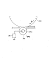
図7は電子写真法における接触帯電の帯電効率例を表わしたグラフである。横軸に接触帯電部材に印加したバイアス、縦軸にはその時得られた被帯電体(以下、感光体と記す)帯電電位を表わすものである。ローラー帯電の場合の帯電特性はAで表わされる。即ち凡そ−500Vの放電閾値を過ぎてから帯電が始まる。従って、−500Vに帯電する場合は−1000Vの直流電圧を印加するか、あるいは、−500V直流の帯電電圧に加えて、放電閾値以上の電位差を常に持つようにピーク間電圧1200Vの交流電圧を印加して感光体電位を帯電電位に収束させる方法が一般的である。
【0025】
より具体的に説明すると、厚さ25μmのOPC感光体に対して帯電ローラーを加圧当接させた場合には、約640V以上の電圧を印加すれば感光体の表面電位が上昇し始め、それ以降は印加電圧に対して傾き1で線形に感光体表面電位が増加する。この閾値電圧を帯電開始電圧Vthと定義する。
つまり、電子写真に必要とされる感光体表面電位Vdを得るためには帯電ローラーにはVd+Vthという必要とされる以上のDC電圧が必要となる。このようにしてDC電圧のみを接触帯電部材に印加して帯電を行なう方法を「DC帯電方式」と称する。
しかし、DC帯電においては環境変動等によって接触帯電部材の抵抗値が変動するため、また、感光体が削れることによって膜厚が変化するとVthが変動するため、感光体の電位を所望の値にすることが難しかった。
【0026】
このため、更なる帯電の均一化を図るために特開昭63−149669号公報に開示されるように、所望のVdに相当するDC電圧に2×Vth以上のピーク間電圧を持つAC成分を重畳した電圧を接触帯電部材に印加する「AC帯電方式」が用いられる。これは、ACによる電位のならし効果を目的としたものであり、被帯電体の電位はAC電圧のピークの中央であるVdに収束し、環境等の外乱には影響されることはない。
ところが、このような接触帯電装置においても、その本質的な帯電機構は、接触帯電部材から感光体への放電現象を用いているため、先に述べたように接触帯電部材に印加する電圧は感光体表面電位以上の値が必要とされ、微量のオゾンは発生する。
【0027】
また、帯電均一化のためにAC帯電を行なった場合にはさらなるオゾンの発生、AC電圧の電界による接触帯電部材と感光体の振動騒音(AC帯電音)の発生、また、放電による感光体表面の劣化等が顕著になり、新たな問題点となっていた。
また、ファーブラシ帯電は、接触帯電部材として導電性繊維のブラシ部を有する部材(ファーブラシ帯電器)を用い、その導電性繊維ブラシ部を被帯電体としての感光体に接触させ、所定の帯電バイアスを印加して感光体面を所定の極性・電位に帯電させるものである。このファーブラシ帯電もその帯電機構は前記▲1▼の放電帯電機構が支配的である。
【0028】
ファーブラシ帯電器は固定タイプとロールタイプが実用化されている。中抵抗の繊維を基布に折り込みパイル状に形成したものを電極に接着したものが固定タイプで、ロールタイプはパイルを芯金に巻き付けて形成する。繊維密度としては100本/mm2 程度のものが比較的容易に得られるが、直接注入帯電により十分均一な帯電を行うにはそれでも接触性は不十分であり、直接注入帯電により十分均一な帯電を行うには感光体に対し機械構成としては困難なほどに速度差を持たせる必要があり、現実的ではない。
このファーブラシ帯電の直流電圧印加時の帯電特性は図7のBに示される特性をとる。従って、ファーブラシ帯電の場合も、固定タイプ、ロールタイプどちらも多くは、高い帯電バイアスを印加し放電現象を用いて帯電を行っている。
【0029】
これらに対し、磁気ブラシ帯電は、接触帯電部材として導電性磁性粒子をマグネットロール等で磁気拘束してブラシ状に形成した磁気ブラシ部を有する部材(磁気ブラシ帯電器)を用い、その磁気ブラシ部を被帯電体としての感光体に接触させ、所定の帯電バイアスを印加して感光体面を所定の極性・電位に帯電させるものである。
この磁気ブラシ帯電の場合はその帯電機構は前記▲2▼の直接注入帯電機構が支配的である。
磁気ブラシ部を構成させる導電性磁性粒子として粒径5〜50μmのものを用い、感光体と十分速度差を設けることで、均一に直接注入帯電を可能にする。
図7の帯電特性グラフのCにあるように、印加バイアスとほぼ比例した帯電電位を得ることが可能になる。
しかしながら、機器構成が複雑であること、磁気ブラシ部を構成している導電性磁性粒子が脱落して感光体に付着する等の弊害もある。
【0030】
ここで、これらの接触帯電方法を現像同時クリーニング方法、クリーナレス画像形成方法に適用した場合を考える。
現像同時クリーニング方法、クリーナレス画像形成方法では、クリーニング部材を有さないために感光体上に残余する転写残トナーが、そのまま接触帯電部材と接触し、付着或いは混入する。また、放電帯電機構が支配的である帯電方法の場合には、放電エネルギーによるトナー劣化に起因する帯電部材への付着性の悪化も生ずる。一般的に用いられている絶縁性トナーが接触帯電部材に付着或いは混入すると、帯電性の低下が起こる。
この被帯電体の帯電性の低下は、放電帯電機構が支配的である帯電方法の場合には、接触帯電部材表面に付着したトナー層が放電電圧を阻害する抵抗となるあたりから急激に起こる。これに対し、直接注入帯電機構が支配的である帯電方法の場合には、付着或いは混入した転写残トナーが接触帯電部材表面と被帯電体との接触確率を低下させることにより被帯電体の帯電性が低下する。
【0031】
この被帯電体の一様帯電性の低下は、画像露光後の静電潜像のコントラスト及び均一性の低下となり、画像濃度を低下させる或いはカブリを増大させる。また、現像同時クリーニング方法、クリーナレス画像形成方法では、感光体上の転写残トナーの帯電極性及び帯電量を制御し、現像工程で安定して転写残トナーを回収し、回収トナーが現像特性を悪化させないようにすることがポイントとなり、転写残トナーの帯電極性及び帯電量の制御を帯電部材によって行うこととなる。
【0032】
これについて具体的に一般的なレイザープリンターを例として説明する。マイナス極性電圧を印加する帯電部材、マイナス帯電性の感光体及びマイナス帯電性のトナーを用いる反転現像の場合、その転写工程において、プラス極性の転写部材によって可視化された像を記録媒体に転写することになるが、記録媒体の種類(厚み、抵抗値、誘電率等の違い)と画像面積等の関係により、転写残余のトナーの帯電極性がプラスからマイナスまで変動する。しかし、マイナス帯電性の感光体を帯電する際のマイナス極性の帯電部材により、感光体表面と共に転写残余のトナーまでもが、転写工程においてプラス極性に振れていたとしても、一様にマイナス側へ帯電極性を揃えることが出来る。これゆえ、現像方法として反転現像を用いた場合、トナーの現像されるべき明部電位部にはマイナスに帯電された、転写残余のトナーが残り、トナーの現像されるべきでない暗部電位には、現像電界の関係上トナー担持体の方に引き寄せられ、暗部電位をもつ感光体上に転写残トナーは残留することなく回収される。すなわち、帯電部材によって感光体の帯電と同時に転写残余のトナーの帯電極性を制御することにより、現像同時クリーニング、クリーナレス画像形成方法が成立する。
【0033】
しかしながら、転写残トナーが接触帯電部材のトナー帯電極性の制御能力以上に、接触帯電部材に付着或いは混入すると、一様に転写残トナーの帯電極性を揃えることができず、現像部材によってトナーを回収することが困難となる。また、トナー担持体に摺擦等の機械的力によって回収されたとしても、転写残トナーの帯電が均一に揃えられていないと、トナー担持体上のトナーの帯電性に悪影響を及ぼし、現像特性を低下させる。
すなわち、現像同時クリーニング、クリーナレス画像形成方法に於ては、転写残トナーの帯電部材通過時の帯電制御特性及び帯電部材への付着・混入特性が、耐久特性、画像品質特性に密接につながっている。
【0034】
帯電ムラを防止し安定した均一帯電を行なうために、接触帯電部材に被帯電体面との接触面に粉末を塗布する構成も特公平7−99442号公報に開示されている。しかしながら、接触帯電部材(帯電ローラー)が被帯電体(感光体)に従動回転(速度差駆動なし)であり、スコロトロン等のコロナ帯電器と比べるとオゾン生成物の発生は格段に少なくなっているものの、帯電原理は前述のローラー帯電の場合と同様に依然として放電帯電機構を主としている。特に、より安定した帯電均一性を得るためにはDC電圧にAC電圧を重畳した電圧を印加するために、放電によるオゾン生成物の発生はより多くなってしまう。よって、長期に装置を使用した場合には、オゾン生成物による画像流れ等の弊害が現れやすい。更に、クリーナーレスの画像形成装置に適用した場合には、転写残トナーの混入のため塗布した粉末が均一に帯電部材に付着していることが困難となり、均一帯電を行なう効果が薄れてしまう。
【0035】
また、特開平5−150539号公報には、接触帯電を用いた画像形成方法において、長時間画像形成を繰り返すうちにブレードクリーニングしきれなかったトナー粒子やシリカ微粒子が帯電手段の表面に付着・蓄積することによる帯電阻害を防止するために、トナー中に、少なくとも顕画粒子と、顕画粒子より小さい平均粒径を有する導電性粒子を含有することが開示されている。しかし、ここで用いられた接触帯電或いは近接帯電は放電帯電機構によるもので、直接注入帯電機構ではなく、放電帯電による前述の問題がある。更に、クリーナーレスの画像形成装置へ適用した場合には、クリーニング機構を有する場合と比較して多量の導電性微粒子及び転写残トナーが帯電工程を通過することによる帯電性への影響、これら多量の導電性微粒子及び転写残トナーの現像工程における回収性、回収された導電性微粒子及び転写残トナーによるトナーの現像特性への影響に関して何ら考慮されていない。更に、接触帯電に直接注入帯電機構を適用した場合には、導電性微粒子が接触帯電部材に必要量供給されず、転写残トナーの影響による帯電不良を生じてしまう。
【0036】
また、近接帯電では、多量の導電性微粒子及び転写残トナーにより感光体を均一帯電することが困難であり、転写残トナーのパターンを均す効果が得られないため転写残トナーのパターン画像露光を遮光するためのパターンゴーストを生ずる。更に、画像形成中の電源の瞬断或いは紙詰まり時にはトナーによる機内汚染が著しくなる。
【0037】
また、現像同時クリーニング画像形成方法に於て、転写残トナーの帯電部材通過時の帯電制御特性を向上させることで現像同時クリーニング性能を向上させるものとして、特開平11−15206号公報では、特定のカーボンブラック及び特定のアゾ系鉄化合物を含有するトナー粒子と無機微粉体とを有するトナーを用いた画像形成方法が提案されている。更に、現像同時クリーニング画像形成方法に於て、トナーの形状係数を規定した転写効率に優れたトナーにより、転写残トナー量を減少させることで現像同時クリーニング性能を向上させることも提案されている。しかしながら、ここで用いられた接触帯電も放電帯電機構によるもので、直接注入帯電機構ではなく、放電帯電による前述の問題がある。更に、これらの提案は、接触帯電部材の転写残トナーによる帯電性低下を抑制する効果はあっても、帯電性を積極的に高める効果は期待できない。
【0038】
更には、市販の電子写真プリンターの中には、転写工程と帯電工程の間に感光体に当接するローラー部材を用い、現像での転写残トナー回収性を補助或いは制御する現像同時クリーニング画像形成装置もある。このような画像形成装置は、良好な現像同時クリーニング性を示し、廃トナー量を大幅に減らすことができるが、コストが高くなり、小型化の点でも現像同時クリーニングの利点を損ねている。
【0039】
これらに対し、特開平10−307456号公報において、トナー粒子及びトナー粒径の1/2以下の粒径を有する導電性を有する帯電促進粒子を含むトナーを直接注入帯電機構を用いた現像同時クリーニング画像形成方法に適用した画像形成装置が開示されている。この提案によると、放電生成物を生ずることなく、廃トナー量を大幅に減らすことが可能な、低コストで小型化に有利な現像同時クリーニング画像形成装置が得られ、帯電不良、画像露光の遮光或いは拡散を生じない良好な画像が得られる。
また、特開平10−307421号公報においては、トナー粒径の1/50〜1/2の粒径を有する導電性粒子を含むトナーを直接注入帯電機構を用いた現像同時クリーニング画像形成方法に適用し導電性粒子に転写促進効果を持たせた画像形成装置が開示されている。
【0040】
更に、特開平10−307455号公報では導電性微粉末の粒径を構成画素1画素の大きさ以下とすること、及びより良好な帯電均一性を得るために導電性微粉末の粒径を10nm〜50μmとすることが記載されている。
特開平10−307457号公報では人の視覚特性を考慮して帯電不良部の画像への影響を視覚的に認識されにくい状態とするために導電性粒子を約5μm以下、好ましくは20nm〜5μmとすることが記載されている。
更に、特開平10−307458号公報によれば、導電性微粉末の粒径はトナー粒径以下とすることで、現像時にトナーの現像を阻害する、あるいは現像バイアスが導電性微粉末を介してリークすることを防止し画像の欠陥をなくすことができること、及び導電性微粉末の粒径を0.1μmより大きく設定することにより、像担持体に導電性微粉末が埋め込まれ露光光を遮光する弊害も解決し優れた画像記録を実現する直接注入帯電機構を用いた現像同時クリーニング画像形成方法が記載されている。
特開平10−307456号公報によれば、トナーに導電性微粉末を外部添加し、少なくとも可穣性の接触帯電部材と像担持体との当接部に前記トナー中に含有の導電性微粉末が、現像工程で像担持体に付着し転写工程の後も像担持体上に残留し持ち運ばれて介在していることで、帯電不良、画像露光の遮光を生じない良好な画像が得られる現像同時クリーニング画像形成装置が開示されている。
【0041】
しかしながら、これらの提案も長期にわたる繰り返し使用における安定した性能、解像性を高めるためにより粒径の小さなトナー粒子を用いる場合の性能に更なる改良の余地があった。
【0042】
【発明が解決しようとする課題】
本発明の目的は、環境に左右されにくく、安定した帯電性能を有し、カブリがなく、長時間の使用においても画像濃度が高く、画像再現性に優れた磁性トナー及び画像形成方法を提供することにある。本発明の目的は、上記のような問題点を解決して、良好な現像同時クリーニング画像形成を可能とする画像形成方法を提供することにある。
【0043】
また、本発明の目的は、良好な帯電性を安定して得られるクリーナーレス画像形成を可能とする画像形成方法を提供することにある。また、本発明の目的は、転写性に優れ、転写残トナーの回収性に優れた現像同時クリーニング画像形成を可能とする画像形成方法を提供することにある。
【0044】
【課題を解決するための手段】
本発明は、像担持体と当接部を形成して接触する帯電部材に電圧を印加することにより、像担持体を帯電する帯電工程と、像担持体の帯電面に静電潜像として画像情報を書き込む静電潜像形成工程と、その静電潜像をトナー担持体上に担持させたトナーによりトナー像として可視化する現像工程と、そのトナー像を記録媒体に転写する転写工程を有し、像担持体上に繰り返して作像が行われ、該帯電工程において、少なくとも帯電部材と像担持体との当接部及び / 又は近傍に、トナー中に含有の導電性微粉末が現像工程で像担持体に付着し転写工程の後も像担持体上に残留し運ばれて介在している画像形成方法に用いられる磁性トナーにおいて、該磁性トナーは、少なくとも結着樹脂及び磁性体を含有する磁性トナー粒子の表面に、無機微粉体及び導電性微粉末を有し、且つ平均円形度が、0.970以上であり、重量平均粒径(D4)が3〜10μmであり、該磁性トナー粒子は、該磁性体として少なくとも磁性酸化鉄を含有しており、該磁性トナーの磁場79.6kA/m(1000エルステッド)における磁化の強さが10〜50Am 2 /kg(emu/g)であり、該磁性トナーのX線光電子分光分析により測定される該磁性トナー粒子の表面に存在する炭素元素の含有量(A)に対する鉄元素の含有量(B)の比(B/A)が、0.001未満であり、該磁性トナーの投影面積円相当径をCとし、透過型電子顕微鏡(TEM)を用いた該磁性トナーの断面観察における磁性体と磁性トナー粒子表面との距離の最小値をDとしたとき、D/C≦0.02の関係を満たす磁性トナー粒子の個数が50%以上であり、該導電性微粉末は、抵抗値が10 9 Ω・cm以下であり、該導電性微粉末は、少なくとも表面が金属酸化物であり、該金属酸化物の主金属に対し0.1〜5原子%のアンチモン原子又はアルミニウム原子を含有する金属酸化物であるか、または、酸素欠損型の金属酸化物であり、該磁性トナー粒子の体積平均粒径よりも小さく且つ体積平均粒径が0.3μ m 以上である導電性微粉末を磁性トナー全体に対して0.2〜10重量%、該磁性トナーは有していることを特徴とする磁性トナー、及び、該磁性トナーを用いた画像形成方法に関する。
【0045】
【発明の実施の形態】
まず、最初に本発明の磁性トナーについて説明し、その後、該トナーを用いた画像形成方法、画像形成装置およびプロセスカートリッジについて説明する。
本発明の磁性トナーは実質上トナー表面に磁性体が露出していない為、粉砕法のトナーと異なりトナーの帯電量がリークし難く、そのため導電性粉体を多く表面に有していても、帯電量の低下が少なく、画像濃度の高い良好な画像を得ることが可能である。また、平均円形度、モード円形度が非常に高い為に磁性トナーが現像部で細い穂を形成し、磁性トナー1個1個の帯電を均一にすることで、かぶりの非常に少ない良好な画像を得ることが可能である。
また、該磁性トナーのX線光電子分光分析により測定される該トナーの表面に存在する炭素元素の含有量(A)に対する鉄元素の含有量(B)の比(B/A)が、0.001未満であることが、トナーの帯電量を保持する上で好ましい。
【0046】
まず、本発明の磁性トナーの特徴である、平均円形度と、磁性トナー粒子の表面に存在する炭素元素の含有量(A)に対する鉄元素の含有量(B)の比(B/A)について説明する。
本発明の磁性トナーは、平均円形度が、0.970以上であるのが好ましい。
平均円形度が0.970以上のトナー(トナー粒子群で構成される粉体)から構成されるトナーは転写性に非常に優れている。これはトナー粒子と感光体との接触面積が小さく、鏡像力やファンデルワールス力等に起因するトナー粒子の感光体への付着力が低下するためと考えられる。従って、このようなトナーを用いれば転写率が高く、転写残トナーが非常に低減するため、帯電部材と感光体との圧接部におけるトナーが非常に少なく、トナー融着が防止され、画像欠陥が著しく抑制されるものと考えられる。
【0047】
さらに、平均円形度が0.970以上のトナー粒子は表面のエッジ部がほとんど無いため、帯電部材と感光体との圧接部において摩擦が低減され、感光体表面の削れが抑制されることも挙げられる。これらの効果は、転写中抜けの発生しやすい接触転写工程を含む画像形成方法においては、より顕著となって現れる。
平均円形度が高い場合でも主として存在する粒子の円形度が低いと効果が不十分な場合もあるため、特に、後に説明するモード円形度が0.990以上であると、円形度が0.990以上の粒子が主として存在することから、上記の効果が顕著に表れるので好ましい。
【0048】
本発明における平均円形度は、粒子の形状を定量的に表現する簡便な方法として用いたものであり、本発明では東亜医用電子製フロー式粒子像分析装置「FPIA−1000」を用いて測定を行い、3μm以上の円相当径の粒子群について測定された各粒子の円径度(ai)を下式(1)によりそれぞれもとめ、さらに下式(2)で示すように測定された全粒子の円形度の総和を、全粒子数(m)で除した値を平均円形度(a)と定義する。
【0049】
【数1】

【数2】
【0051】
なお、本発明で用いている測定装置である「FPIA−1000」は、各粒子の円形度を算出後、平均円形度およびモード円形度の算出に当たって、粒子を得られた円形度によって、円形度0.40〜1.00を61分割したクラスに分け、分割点の中心値と頻度を用いて平均円形度及びモード円形度の算出を行う算出を行う算出法を用いている。しかしながら、この算出式で算出される平均円形度及びモード円形度の各値との誤差は、非常に少なく、実質的に無視出来る程度のものであり、本発明においては、算出時間の短縮化や算出演算式の簡略化の如きデータの取り扱い上の理由で、上述した各粒子の円形度を直接用いる算出式の概念を利用し、一部変更したこのような算出式を用いても良い。
【0052】
測定手段としては以下の通りである。界面活性剤を約0.1mg溶解している水10mlに現像剤5mgを分散させて分散液を調製し、超音波(20KHz、50W)を分散液に5分間照射し、分散液濃度を5000〜2万個/μlとして前記装置により測定を行い、3μm以上の円相当径の粒子群の平均円形度及びモード円形度を求める。
本発明における平均円形度とは、現像剤の凹凸の度合いの指標であり、現像剤が完全な球形の場合1.000を示し、表面形状が複雑になるほど円形度は小さな値となる。
【0053】
なお、本測定において3μm以上の円相当径の粒子群についてのみ円形度を測定する理由は、3μm未満の円相当径の粒子群にはトナー粒子とは独立して存在する外部添加剤の粒子群も多数含まれるため、その影響によりトナー粒子群についての円形度が正確に見積もれないからである。
【0054】
また、本発明の磁性トナー粒子は、磁性体として少なくとも磁性酸化鉄を含有する。そして、本発明の磁性トナーは、X線光電子分光分析により測定される該磁性トナー粒子の表面に存在する炭素元素の含有量(A)に対する鉄元素の含有量(B)の比(B/A)が、0.001未満であることを特徴とする。この比(B/A)は、0.0005未満であるのが好ましい。
本発明のトナーにおいてはトナー粒子が高い帯電量を持つことが好ましく、そのためには表面に電荷のリークサイトとなる磁性体が露出していないことが好ましい。
【0055】
通常、接触帯電工程を含む画像形成方法において、トナー粒子表面に磁性体が露出している磁性トナーを用いた場合、露出した磁性体による感光体の削れがより顕著となって現れやすい。しかしながら、上述のように(B/A)が0.001未満である、すなわち磁性体がトナー粒子表面に実質的にほとんど露出していない磁性トナーを用いれば、帯電部材によりトナーが感光体表面に圧接されても感光体表面が削れることはほとんど無く、感光体の削れやトナー融着を著しく低減させることが可能となる。接触転写工程を組み合わせた画像形成方法においてもその効果は非常に大きく、非常に高精細な画像を長期に渡って得ることが可能である。
【0056】
トナー粒子表面に存在する炭素元素の含有量(A)に対する鉄元素の含有量(B)の比(B/A)は、以下のように、ESCA(X線光電子分光分析)により表面組成分析を行うことにより測定できる。
本発明では、ESCAの装置および測定条件は、下記の通りである。
【0057】
使用装置:PHI社製 1600S型 X線光電子分光装置
測定条件:X線源 MgKα(400W)
分光領域 800μmφ
本発明では、測定された各元素のピーク強度から、PHI社提供の相対感度因子を用いて表面原子濃度を算出した。
本測定はトナーを超音波洗浄し、トナー粒子表面に付着している外添剤を除去した後、磁気力にて分離し、乾燥し測定することが好ましい。
【0058】
次に、磁性トナーの粒径について説明する。
本発明の画像形成方法において、更に高画質化のため、より微小な潜像ドットを忠実に現像するためには、本発明の磁性トナーの重量平均径は3μm〜10μmであることが必要である。この磁性トナーの重量平均径は、4μm〜8μmであることが好ましい。重量平均径が3μm未満のトナーにおいては、転写効率の低下から感光体上の転写残トナーが多くなり、接触帯電工程での感光体の削れやトナー融着の抑制が難しくなる。さらに、トナー全体の表面積が増えることに加え、粉体としての流動性及び攪拌性が低下し、個々のトナー粒子を均一に帯電させることが困難となることからカブリや転写性が悪化傾向となり、削れや融着以外にも画像の不均一ムラの原因となりやすいため、本発明で使用するトナーには好ましくない。また、トナーの重量平均径が10μmを越える場合には、文字やライン画像に飛び散りが生じやすく、高解像度が得られにくい。さらに装置が高解像度になっていくと8μm以上のトナーは1ドットの再現が悪化する傾向にある。
また、本発明の磁性トナーのモード円形度は、0.990以上であることが好ましい。さらに本発明の磁性トナーにおいては重量平均粒径(D4)と数平均粒径(D1)の比D4/D1が1.4未満である粒度分布を持つことが好ましい。特に重合法でトナー粒子を製造する際に、トナー粒子表面に磁性粉体が露出しているとトナー粒子の粒度分布を悪化させる傾向にある。
【0059】
本発明のトナーの重量平均粒径及び数平均粒径はコールターカウンターTA−II型あるいはコールターマルチサイザー(コールター社製)等種々の方法で測定可能である。具体的には、下記のように測定できる。コールターマルチサイザー(コールター社製)を用い、個数分布、体積分布を出力するインターフェイス(日科機製)及びPC9801パーソナルコンピューター(NEC製)を接続し、電解液は1級塩化ナトリウムを用いて1%NaCl水溶液を調整する。たとえば、ISOTON R−II(コールターサイエンティフィックジャパン社製)が使用できる。測定手順は以下の通りである。前記電解水溶液を100〜150ml加え、更に測定試料を2〜20mg加える。試料を懸濁した電解液は超音波分散器で約1〜3分間分散処理を行ない前記コールターマルチサイザーによりアパーチャーを用いて、2μm以上のトナー粒子の体積、個数を測定して体積分布と個数分布とを算出する。それから、本発明に係わる所の体積分布から求めた体積基準の重量平均粒径(D4)及び個数分布から求めた個数基準の長さ平均粒径、すなわち数平均粒径(D1)を求める。
また、本発明の磁性トナーは表面に実質上磁性体が露出していない為、高く均一な帯電量を有するが、導電性粉体を表面に有することにより、低温低湿化における多数枚画だしにおいても良好な画像を得ることが可能である。
【0060】
なお、粒子内部の特定の部分のみに磁性体粒子が含有されている特殊なトナーは、特開平7−209904号公報においても既に開示されている。
しかしながら、特開平7−209904号公報においては、開示されているトナーの平均円形度に関する言及がなされていない。
さらに、特開平7−209904号公報において開示されているトナー構成を要約すれば、トナー粒子表面付近に磁性体粒子の存在しない樹脂層が一定量以上の厚みで形成されている構造から成るものであり、これは、磁性体粒子が存在しないトナー表層部分がかなりの割合で存在することを意味している。しかしながら言い換えると、このようなトナーは、例えば平均粒径が10μmと小さい場合、磁性体粒子が存在しうる容積が小さくなるため、十分な量の磁性体粒子を内包しにくいということでもある。しかも、こういったトナーでは、トナーの粒度分布において粒径の大きいトナー粒子と小さい粒子とでは磁性体粒子の存在しない表面樹脂層の割合が異なる。従って、内包される磁性体含有量も異なるため、現像性や転写性もトナーの粒径によって異なってしまい、粒径に依存する、選択現像性が見られやすい。従って、こういった磁性トナーで長期にわたり印刷を行うと、磁性体を多く含み現像されにくい粒子、即ち粒径の大きなトナー粒子が残りやすく、画像濃度及び画質の低下、さらには定着性の悪化にもつながる。
【0061】
上記の説明から導かれるように、トナー粒子中における好ましい磁性体分散状態とは、磁性体粒子が凝集せずになるべくトナー粒子全体に均一に存在する状態であり、これもまた本発明の画像形成方法に係わる磁性トナーの特徴である。
即ち、磁性トナーの投影面積円相当径をCとし、透過型電子顕微鏡(TEM)を用いた該磁性トナーの断面観察において、磁性体とトナー粒子表面との距離の最小値をDとしたとき、D/C≦0.02の関係を満たすトナー粒子の個数が50%以上であることもまた、本発明の磁性トナーに必要な態様の一つである。
本発明においては、D/C≦0.02以下の関係を満たすトナー粒子の数が50%以上であることが好ましく、65%以上がより好ましく、75%以上がさらに好ましい。
【0062】
D/C≦0.02以下の関係を満たすトナー粒子数が50%未満の場合には、過半数のトナー粒子において少なくともD/C=0.02境界線よりも外側には磁性粒子が全く存在しないことになる。仮にこのような粒子を球形として想定すると、1つのトナー粒子を全空間とした場合に磁性体の存在しない空間は、トナー粒子の表面に少なくとも11.5%は存在することになる。実際には、最近接位置に磁性粒子が均一に整列してトナー粒子内部に内壁を作るように存在するわけではないので12%以上になることは明らかである。このような粒子から構成される磁性トナーにおいては、上述の如き様々な弊害が生じやすい。
【0063】
本発明において、TEMによる具体的なD/Cの測定方法としては、常温硬化性のエポキシ樹脂中へ観察すべき粒子を十分に分散させた後に温度40℃の雰囲気中で2日間硬化させ得られた硬化物を、そのまま、あるいは凍結してダイヤモンド歯を備えたミクロトームにより薄片状のサンプルとして観察する方法が好ましい。
【0064】
該当する粒子数の割合の具体的な決定方法については、以下のとおりである。TEMにてD/Cを決定するための粒子は、顕微鏡写真での断面積から円相当径を求め、その値が数平均粒径の±10%の幅に含まれるものを該当粒子とし、その該当粒子について、磁性粒子表面との距離の最小値(D)を計測し、D/Cを計算する。このようにして計算されたD/C値が0.02以下の粒子の割合を、下記式により求めるものと定義する。このときの顕微鏡写真は精度の高い測定を行うために、1万〜2万倍の倍率が好適である。本発明では、透過型電子顕微鏡(日立製H−600型)を装置として用い、加速電圧100kVで観察し、拡大倍率が1万倍の顕微鏡写真を用いて観察・測定した。
【0065】
【数3】
【0066】
本発明の磁性トナー粒子は重合法によって得られる粒子であるのが好ましい。本発明に係わるトナーは、粉砕法によって製造することも可能であるが、この粉砕法で得られるトナー粒子は一般に不定形のものであり、本発明に係わるトナーの必須要件である平均円形度が0.970以上、(好ましくはモード円形度が0.990以上)という物性を得るためには機械的・熱的あるいは何らかの特殊な処理を行うことが必要となる。さらに粉砕法は、本質的にトナー粒子表面に磁性酸化鉄粒子が露出してしまうため、本発明の画像形成方法に不可欠な条件である、X線光電子分光分析により測定される表面に存在する炭素元素の含有量(A)に対する鉄元素の含有量(B)の比(B/A)が、0.001未満であるトナーを得ることが困難であり、感光体の削れという問題が解決できない。
【0067】
そこで、上述の諸問題を解決するため、本発明においては、トナー粒子を重合法により製造することが好ましい。トナーの重合法としては、直接重合法、懸濁重合法、乳化重合法、乳化会合重合法、シード重合法等が挙げられるが、これらの中では、粒径と粒子形状のバランスのとりやすさという点で、特に懸濁重合法により製造することが好ましい。
この懸濁重合法においては重合性単量体および着色剤(更に必要に応じて重合開始剤、架橋剤、荷電制御剤、その他の添加剤)を均一に溶解または分散せしめて単量体組成物とした後、この単量体組成物を分散安定剤を含有する連続層(例えば水相)中に適当な撹拌器を用いて分散し同時に重合反応を行なわせ、所望の粒径を有するトナーを得るものである。この懸濁重合法で得られるトナー(以後重合トナー)は、個々のトナー粒子形状がほぼ球形に揃っているため、平均円形度が0.970以上、特にモード円形度が0.990以上という物性要件を満たすトナーが得られやすく、さらにこういったトナーは帯電量の分布も比較的均一となるため高い転写性を有している。
【0068】
しかしながら、重合トナー中に通常の磁性体を含有させても、粒子表面からの磁性体の露出を抑えることは難しい。さらにはトナー粒子の流動性及び帯電特性が著しく低下するだけでなく、懸濁重合トナーの製造時に磁性体と水との相互作用が強いことにより、平均円形度が0.970以上のトナーが得られ難い。これは、▲1▼磁性体粒子は一般的に親水性であるためにトナー表面に存在しやすいこと、▲2▼水溶媒撹拌時に磁性体が乱雑に動き、それに単量体から成る懸濁粒子表面が引きずられ、形状が歪んで円形になりにくいこと、等が原因と考えられる。こういった問題を解決するためには磁性体粒子の有する表面特性の改質が重要である。重合トナーに使用される磁性体の表面改質に関しては、数多く提案されている。例えば、特開昭59−200254号公報、特開昭59−200256号公報、特開昭59−200257号公報、特開昭59−224102号公報等に磁性体の各種シランカップリング剤処理技術が提案されており、特開昭63−250660号公報では、ケイ素元素含有磁性粒子をシランカップリング剤で処理する技術が開示されている。
【0069】
しかしながら、これらの処理によりトナー粒子表面からの磁性体の露出はある程度抑制されるものの、磁性体表面の疎水化を均一に行うことが困難であるという問題があり、したがって、磁性体同士の合一や疎水化されていない磁性体粒子の発生を避けることができず、磁性体の露出を完全に抑制するには不十分である。また、疎水化磁性酸化鉄を用いる例として特公昭60−3181号公報にアルキルトリアルコキシシランで処理した磁性酸化鉄を含有するトナーが提案されている。この磁性酸化鉄の添加により、確かにトナーの電子写真諸特性は向上しているものの、磁性酸化鉄の表面活性は元来小さく、処理の段階で合一粒子が生じたり、疎水化が不均一であったりで、必ずしも満足のいくものではなく、本発明の画像形成方法に適用するにはさらなる改良が必要である。さらに、処理剤等を多量に使用したり、高粘性の処理剤等を使用した場合、疎水化度は確かに上がるものの、粒子同士の合一等が生じて分散性は逆に悪化してしまう。このような磁性体を用いて製造されたトナーは、摩擦帯電性が不均一であり、それに起因してカブリや転写性が良くないものとなる。
【0070】
このように、従来の表面処理磁性体を用いた重合トナーでは、疎水性と分散性の両立は必ずしも達成されておらず、このような重合トナーを本発明のような接触帯電工程から成る画像形成方法に適用しても、高精細な画像を安定して得ることは難しい。
【0071】
そこで、本発明の画像形成方法に関わる磁性トナーに使用される磁性体においては、その粒子表面を疎水化する際、水系媒体中で、磁性体粒子を一次粒径となるよう分散しつつカップリング剤を加水分解しながら表面処理する方法を用いることが特に好ましい。この疎水化処理方法は気相中で処理するより、磁性体粒子同士の合一が生じにくく、また疎水化処理による磁性体粒子間の帯電反発作用が働き、磁性体はほぼ一次粒子の状態で表面処理される。
カップリング剤を水系媒体中で加水分解しながら磁性体表面を処理する方法は、クロロシラン類やシラザン類のようにガスを発生するようなカップリング剤を使用する必要もなく、さらに、これまで気相中では磁性体粒子同士が合一しやすくて、良好な処理が困難であった高粘性のカップリング剤も使用できるようになり、疎水化の効果は非常に大きい。
【0072】
本発明に係わる磁性体の表面処理において使用できるカップリング剤としては、例えば、シランカップリング剤、チタンカップリング剤等が挙げられる。より好ましく用いられるのはシランカップリング剤であり、下記の一般式(I)で示されるものである。
【0073】
【化3】
Rm−Si−Yn (I)
[式中、Rはアルコオキシ基を示し、mは1〜3の整数を示し、Yはアルキル基、ビニル基、グリシドキシ基、メタクリル基の如き炭化水素基を示し、nは1〜3の整数を示す。]
具体的には、ビニルトリメトキシシラン、ビニルトリエトキシシラン、γ−メタクリルオキシプロピルトリメトキシシラン、ビニルトリアセトキシシラン、メチルトリメトキシシラン、メチルトリエトキシシラン、イソブチルトリメトキシシラン、ジメチルジメトキシシラン、ジメチルジエトキシシラン、トリメチルメトキシシラン、ヒドロキシプロピリトリメトキシシラン、フェニルトリメトキシシラン、n−ヘキサデシルトリメトキシシラン、n−オクタデシルトリメトキシシラン等を挙げることができる。
【0074】
特に、下記の一般式(II)で示されるアルキルトリアルコキシシランカップリング剤を使用して水系媒体中で磁性粒子を疎水化処理するのが良い。
【0075】
【化4】
CpH2p+1−Si−(OCqH2q+1)3 (II)
[式中、pは2〜20の整数を示し、qは1〜3の整数を示す。]
上記式(II)におけるpが、2より小さいと、疎水化処理は容易となるが、疎水性を十分に付与することが困難であり、トナー粒子からの磁性粒子の露出を抑制するのが難しくなる。またpが20より大きいと、疎水性は十分になるが、磁性体粒子同士の合一が多くなり、トナー中へ磁性体粒子を十分に分散性させることが困難になり、カブリや転写性が悪化傾向となる。
また、qが、3より大きいとシランカップリング剤の反応性が低下して疎水化が十分に行われにくくなる。
特に、式中のpが2〜20の整数(より好ましくは、3〜15の整数)を示し、qが1〜3の整数(より好ましくは、1又は2の整数)を示すアルキルトリアルコキシシランカップリング剤を使用するのが良い。
その処理量は磁性体100質量部に対して、0.05〜20質量部、好ましくは0.1〜10質量部とするのが良い。
【0076】
ここで、水系媒体とは、水を主要成分としている媒体である。具体的には、水系媒体として水そのもの、水に少量の界面活性剤を添加したもの、水にpH調製剤を添加したもの、水に有機溶剤を添加したものが挙げられる。界面活性剤としては、特に限定されるものではないが、ポリビニルアルコール等のノンイオン系界面活性剤を使用するのが好ましい。界面活性剤は、水に対して0.1〜5wt%添加するのが好ましい。pH調製剤としては、例えば、塩酸のような無機酸が挙げられる。有機溶剤としては、例えば、メタノール等が挙げられ、水に対して0〜500wt%添加するのが好ましい。
【0077】
撹拌は、例えば撹拌羽根を有する混合機(具体的には、アトライター、TKホモミキサーの如き高剪断力混合装置)で、磁性体粒子が水系媒体中で、一次粒子になるように充分におこなうのが良い。
こうして得られる磁性体は粒子の凝集が見られず、個々の粒子表面が均一に疎水化処理されているため、重合トナー用の材料として用いた場合、トナー粒子中への分散性が非常に良好である。しかもトナー粒子表面からの露出が無く、ほぼ球形に近い、粒度分布の狭い重合トナー粒子が得られる。従って、こういった磁性体を用いることにより、平均円形度が0.970以上、特にはモード円形度が0.990以上で、X線光電子分光分析により測定されるトナーの表面に存在する炭素元素の含有量(A)に対する鉄元素の含有量(B)の比(B/A)が0.001未満という磁性トナーを得ることが可能となる。
【0078】
そして、このトナーを接触帯電工程を有する本発明の画像形成方法で用いると、感光体の削れやトナー融着がより一層抑制され、低湿環境下においても高画質の安定化が達成できるのである。さらには、(B/A)を0.0005未満とすれば、高画質及び耐久安定性が格段に向上するので更に好ましい。
本発明の磁性トナーは、結着樹脂に対して0.5〜50重量%の離型剤を含有することも好ましい。結着樹脂としては、後述するように例えば、各種のワックス等が例示できる。
転写材上に転写されたトナー像はその後、熱・圧力等のエネルギーにより転写材上に定着され、半永久的画像が得られる。この際、熱ロール式定着が一般に良く用いられる。
【0079】
前述のように、重量平均粒径が10μm以下のトナー粒子を用いれば非常に高精細な画像を得ることができるが、粒径の細かいトナー粒子は紙等の転写材を使用した場合に紙の繊維の隙間に入り込み、熱定着用ローラーからの熱の受け取りが不十分となり、低温オフセットが発生しやすい。しかしながら、本発明に係わるトナーにおいて、適正量の離型剤を含有させることにより、高解像性と耐オフセット性を両立させつつ感光体の削れを防止することが可能となる。
【0080】
本発明に係わるトナーに使用可能な離型剤としては、パラフィンワックス、マイクロクリスタリンワックス、ペトロラクタム等の石油系ワックス及びその誘導体、モンタンワックス及びその誘導体、フィッシャートロプシュ法による炭化水素ワックス及びその誘導体、ポリエチレンに代表されるポリオレフィンワックス及びその誘導体、カルナバワックス、キャンデリラワックス等天然ワックス及びその誘導体などである。これらの誘導体には酸化物や、ビニル系モノマーとのブロック共重合物、グラフト変性物を含む。さらには、高級脂肪族アルコール、ステアリン酸、パルミチン酸等の脂肪酸、あるいはその化合物、酸アミドワックス、エステルワックス、ケトン、硬化ヒマシ油及びその誘導体、植物系ワックス、動物性ワックス等が挙げられる。これらのワックスの中では、示差熱分析における吸熱ピークが40℃〜110℃であるものが好ましく、更には45℃〜90℃であるものが好ましい。離型剤を使用する際の含有量としては、結着樹脂に対して0.5〜50重量%の範囲が好ましい。含有量が0.5重量%未満では低温オフセット抑制効果に乏しく、50重量%を超えてしまうと長期間の保存性が悪化すると共に、他のトナー材料の分散性が悪くなり、トナーの流動性の悪化や画像特性の低下につながる。
【0081】
本発明の画像形成方法に関わるトナーには、荷電特性を安定化するために荷電制御剤を配合しても良い。荷電制御剤としては、公知のものが利用でき、特に帯電スピードが速く、かつ、一定の帯電量を安定して維持できる荷電制御剤が好ましい。さらに、トナーを直接重合法を用いて製造する場合には、重合阻害性が低く、水系分散媒体への可溶化物が実質的にない荷電制御剤が特に好ましい。具体的な化合物としては、ネガ系荷電制御剤としてサリチル酸、アルキルサリチル酸、ジアルキルサリチル酸、ナフトエ酸、ダイカルボン酸の如き芳香族カルボン酸の金属化合物、アゾ染料あるいはアゾ顔料の金属塩または金属錯体、スルホン酸又はカルボン酸基を側鎖に持つ高分子型化合物、ホウ素化合物、尿素化合物、ケイ素化合物、カリックスアレーン等が挙げられる。ポジ系荷電制御剤として四級アンモニウム塩、該四級アンモニウム塩を側鎖に有する高分子型化合物、グアニジン化合物、ニグロシン系化合物、イミダゾール化合物等が挙げられる。
【0082】
電荷制御剤をトナーに含有させる方法としては、トナー母粒子内部に添加する方法と外添する方法がある。これらの電荷制御剤の使用量としては、結着樹脂の種類、他の添加剤の有無、分散方法を含めたトナー製造方法によって決定されるもので、一義的に限定されるものではないが、好ましくは結着樹脂100質量部に対して0.1〜10質量部、より好ましくは0.1〜5質量部の範囲で用いられる。
【0083】
本発明のトナーをネガトナーとする際には、アゾ染料もしくはアゾ顔料の金属塩またはそれらの金属錯体が好ましく用いられ、特には、下記一般式(III)で表わされるアゾ系鉄錯体化合物を含有することが、望ましい。
【0084】
【化5】
また、本発明の磁性トナーは、少なくとも結着樹脂中に着色剤及び上記の一般式(III)で表わされるアゾ系鉄錯体化合物を含有する磁性トナーであるのが好ましい。
本発明のような特殊な形状のトナーを低温低湿環境下で画出しテストを行うと、トナー担持体上のトナーの薄層コート層の均一性が乱れやすく、ベタ画像上にかすれ/波状のむら等の画像欠陥が現れやすいことがわかった。
本発明者らは、このコート層の不均一が、この特殊な形状に起因して、トナーの表面積当りの帯電量が従来のトナーに比べて高くなりやすいために起こることを見いだした。
その原因としては、トナー表面に凹凸が少なく、トナー担持体表面と接触する機会がより多いためではないかと考えている。
【0085】
そこでトナーの帯電制御性を従来以上に高めるために、トナーの荷電制御剤に関して検討をするなかで、上記構造を有する特定のアゾ系鉄錯体化合物を用いることにより、トナー担持体上のトナーの薄層コート層の均一性乱れが解決できることを見いだした。
【0086】
本発明に、荷電制御剤として特定のアゾ系鉄錯体化合物を用いる理由としては、例えば従来用いられてきた荷電制御剤では、低湿下でチャージアップする傾向があり、トナーの単位体積当りの帯電量が高くなり過ぎて、トナー担持体上に均一にコートされないという欠点があった。これに対して、本発明のアゾ系鉄錯体化合物では、帯電を制御することができ、トナー担持体上に均一にコートすることができるからである。
【0087】
さらに本発明者らが検討したところ、前記一般式に示したアゾ系鉄錯体化合物のA+が75〜98モル%のアンモニウムイオンを含有することが、安定したトナー画像を得るために好ましい傾向を示すことを見いだした。即ち、前記アゾ系鉄錯体化合物においてアンモニウムイオンだけをカチオンとして有する場合には、高湿下に放置後の画像濃度の立ち上がりが遅くなる傾向が見られる。
一方、プロトンやアルカリ金属だけをカチオンとして有する場合には、高湿下で画像濃度が低めに推移する。
【0088】
本発明者らが検討したところ、カチオン成分としてアンモニウムイオンおよびアルカリ金属イオンおよび/またはプロトンを共存させることで、長期放置特性の良好な化合物が得られることを新たに見いだした。特に、アンモニウムイオンが75〜98モル%になると画像濃度の立ち上がり、及び立ち上がった濃度レベルが良好になる。
アンモニウムイオンが75%未満になると、画像濃度が低くなり、98%を超えると、画像濃度の立ち上がりが遅くなる傾向が見られる。
前記一般式のアゾ系鉄錯体化合物の代表的な具体例としては、次のような化合物が挙げられる。
【0089】
【化6】
【化7】
【化8】
【化9】
【化10】
【化11】
【0095】
本発明の磁性トナーは、結着樹脂及び磁性体を含有する磁性トナー粒子の表面に無機微粉体と導電性微粉末とを有するものである。
次に、本発明の磁性トナーに含まれる磁性体および結着樹脂について説明する。本発明の磁性トナー粒子は、磁性体として少なくとも、マグネタイト、マグヘマイト、フェライト等の磁性酸化鉄を含有する。
【0096】
本発明においてトナーを磁性トナーとするためトナー母粒子に含有させる磁性体としては、マグネタイト、マグヘマイト、フェライト等の磁性酸化鉄、鉄、コバルト、ニッケル等の金属或いはこれらの金属とアルミニウム、コバルト、銅、鉛、マグネシウム、錫、亜鉛、アンチモン、ベリリウム、ビスマス、カドミウム、カルシウム、マンガン、セレン、チタン、タングステン、バナジウム等の金属の合金及びその混合物が挙げられる。これら磁性体は、窒素吸着法によるBET比表面積が好ましくは2〜30m2/g、特に3〜28m2/g、更にモース硬度が5〜7のものが好ましい。
【0097】
本発明で使用される磁性トナーに用いられる磁性体は、結着樹脂100質量部に対して、10質量部〜200質量部を用いることが好ましい。さらに好ましくは20〜180質量部を用いることが良い。10質量部未満ではトナーの着色力が乏しく、カブリの抑制も困難である。一方、200質量部を越えると、トナー担持体への磁力による保持力が強まり現像性が低下したり、個々のトナー粒子への磁性体の均一な分散が難しくなるだけでなく、定着性が低下してしまう。
【0098】
本発明の画像形成方法に係わる磁性トナーに用いられる磁性体は、例えばマグネタイトの場合、下記方法で製造することができる。
第一鉄塩水溶液に、鉄成分に対して当量または当量以上の水酸化ナトリウムの如きアルカリを加え、水酸化第一鉄を含む水溶液を調製する。調製した水溶液のpHをpH7以上(好ましくはpH8〜10)に維持しながら空気を吹き込み、水溶液を70℃以上に加温しながら水酸化第一鉄の酸化反応をおこない、磁性酸化鉄粒子の芯となる種晶をまず生成する。
【0099】
次に、種晶を含むスラリー状の液に前に加えたアルカリの添加量を基準として約1当量の硫酸第一鉄を含む水溶液を加える。液のpHを6〜10に維持しながら空気を吹込みながら水酸化第一鉄の反応をすすめ種晶を芯にして磁性酸化鉄粒子を成長させる。酸化反応がすすむにつれて液のpHは酸性側に移行していくが、液のpHは6未満にしない方が好ましい。酸化反応の終期に液のpHを調製し、磁性酸化鉄が一次粒子になるよう十分に攪拌し、カップリング剤を添加して十分に混合攪拌し、攪拌後に濾過し、乾燥し、軽く解砕することで疎水性処理磁性酸化鉄粒子が得られる。また、酸化反応終了後、洗浄、濾過して得られた酸化鉄粒子を、乾燥せずに別の水系媒体中に再分散させた後、再分散液のpHを調製し、十分攪拌しながらシランカップリング剤を添加し、カップリング処理を行っても良い。酸化反応終了後に乾燥工程を経ずに表面処理を行うことが肝要である。
【0100】
第一鉄塩としては、一般的に硫酸法チタン製造に副生する硫酸鉄、鋼板の表面洗浄に伴って副生する硫酸鉄の利用が可能であり、更に塩化鉄等が利用可能である。水溶液法による磁性酸化鉄の製造方法は一般に反応時の粘度の上昇を防ぐこと、及び、硫酸鉄の溶解度から鉄濃度0.5〜2mol/lが用いられる。硫酸鉄の濃度は一般に薄いほど製品の粒度が細かくなる傾向を有する。又、反応に際しては、空気量が多い程、そして反応温度が低いほど微粒化しやすい。
このようにして製造された疎水性磁性体粒子を材料とした磁性トナーを使用することにより、感光体の削れ及びトナー融着が発生せず、高画質及び高安定性が可能となる。
【0101】
また、磁性体の形状としては、8面体、6面体、球状、針状、鱗片状などがあるが、8面体、6面体、球状、不定形等の異方性の少ないものが画像濃度を高める上で好ましい。こういった磁性体の形状は、SEMなどによって確認することができる。磁性体の粒度としては、体積平均粒径が、0.1〜0.3μmであり、かつ0.03〜0.1μm以下の粒子の個数%が40%以下であることが好ましい。
【0102】
平均粒径が0.1μm未満の磁性粉体を用いた磁性トナーから画像を得ると、画像の色味が赤味にシフトし、画像の黒色度が不足したり、ハーフトーン画像ではより赤味が強く感じられる傾向が強くなるなど、一般的に好ましいものではない。また、このようなトナーをカラー画像に用いた場合には、色再現性が得られにくくなったり、色空間の形状がいびつになる傾向があるため好ましくない。さらに、磁性粉体の表面積が増大するために分散性が悪化し、製造時に要するエネルギーが増大し、効率的ではない。また、磁性粉体の添加量から得られるべき画像の濃度が不足することもあり、好ましいものではない。
【0103】
一方、磁性粉体の平均粒径が0.3μmを超えると、一粒子あたりの質量が大きくなるため、製造時にバインダーとの比重差の影響でトナー表面に露出する確率が高まったり、製造装置の摩耗などが著しくなる可能性が高まったり、分散物の沈降安定性などが低下するため好ましくない。
また、トナー中において、該磁性体の0.1μm以下の粒子の個数%が40%を超えると、磁性粉体の表面積が増大して分散性が低下し、トナー中にて凝集塊を生じやすくなりトナーの帯電性を損なったり、着色力が低下したりする可能性が高まるため40%以下でなければならない。
【0104】
さらに、30%以下とすると、その傾向はより小さくなるため、より好ましい。
尚、0.03μm未満の磁性体は、粒子径が小さいことに起因してトナー製造時に受ける応力が小さいため、トナー粒子の表面へ出る確率が低くなる。さらに、仮に粒子表面に露出してもリークサイトとして作用することはほとんど無く実質上問題とならない。そのため、本発明では、0.03〜0.1μmの粒子に注目し、その個数%を定義するものである。
また、磁性粉体中の0.3μm以上の粒子が10個数%を超えると、着色力が低下し、画像濃度が低下する傾向になるので、好ましくない。より好ましくは5個数%以下とするのが良い。
【0105】
本発明においては、前述の粒度分布の条件を満たすよう、磁性体製造条件を設定したり、予め粉砕及び分級の如き粒度分布の調整を行ったものを使用することが好ましい。分級方法としては、例えば、遠心分離やシックナーといった沈降分離を利用したものや、例えばサイクロンを利用した湿式分級装置などの手段が好適である。
【0106】
本発明において磁性体の体積平均粒径および粒度分布の決定は、以下の測定方法によって行う。
粒子を十分に分散させた状態で、透過型電子顕微鏡(TEM)において3万倍の拡大倍率の写真で視野中の100個の磁性体粒子のそれぞれ投影面積を測定し、測定された各磁性体粒子の投影面積に等しい円の相当径を各磁性体粒子径として求めた。さらに、その結果を基に、体積平均粒径の算出ならび0.03〜0.1μmの粒子と、0.3μm以上の粒子の個数%を計算した。また、画像解析装置により粒子径を測定することも可能である。
【0107】
トナー粒子中の磁性体の体積平均粒径および粒度分布を決定する場合には、以下の測定方法により行う。
エポキシ樹脂中へ観察すべきトナー粒子を十分に分散させた後、温度40℃の雰囲気中で2日間硬化させ得られた硬化物を、ミクロトームにより薄片状のサンプルとして、透過型電子顕微鏡(TEM)において1万〜4万倍の拡大倍率の写真で視野中の100個の磁性粒子径のそれぞれ投影面積を測定し、測定された各磁性体粒子の投影面積に等しい円の相当径を各磁性体粒子径として求めた。さらに、その結果を基に、0.03〜0.1μmの粒子と、0.3μm以上の粒子の個数%を計算した。また、画像解析装置により粒子径を測定することも可能である。
【0108】
これらの磁性体の磁気特性としては、磁場795.8kA/m下で飽和磁化が10〜200Am2/kg、残留磁化が1〜100Am2/kg、抗磁力が1〜30kA/mであるものが用いられる。これらの磁性体は結着樹脂100質量部に対し、20〜200質量部で用いられる。このような磁性体の中でもマグネタイトを主とするものが特に好ましい。
【0109】
本発明において磁性トナーの磁化の強さは、振動型磁力計VSM P−1−10(東英工業社製)を用いて、25℃の室温にて外部磁場79.6kA/mで測定した。また、磁性体の磁気特性は、25℃の室温にて外部磁場796kA/mで測定した。
また、本発明の磁性トナーは、磁場79.6kA/m(1000エルステッド)における磁化の強さが10〜50Am2/kg(emu/g)である磁性トナーであることが必要である。
【0110】
本発明において磁場79.6kA/mにおける磁化の強さを規定する理由は、磁性体の磁気特性を表わす量としては、磁気飽和における磁化の強さ(飽和磁化)が用いられるが、本発明においては画像形成装置内で実際に磁性トナーに作用する磁場における磁性トナーの磁化の強さが重要であるためである。画像形成装置に磁性トナーが適用される場合、磁性トナーに作用する磁場は、画像装置外への磁場の漏洩を大きくしないため或いは磁場発生源のコストを低く抑えるために、市販されている多くの画像形成装置において数十から百数十kA/mであり、画像形成装置内で実際に磁性トナーに作用する磁場の代表的な値として磁場79.6kA/m(1000エルステッド)を選択し、磁場79.6kA/mにおける磁化の強さを規定した。
【0111】
現像装置内に磁気力発生手段を設けることで、磁性トナーではトナーの漏れを防止でき、トナーの搬送性或いは攪拌性を高められるばかりでなく、トナー担持体上に磁力が作用するように磁気力発生手段を設けることで、転写残トナーの回収性が更に向上し、又磁性トナーが穂立ちを形成するためにトナーの飛散を防止することが容易となる。しかし、トナーの磁場79.6kA/mにおける磁化の強さが10Am2/kg未満であると、上記の効果が得られず、トナー担持体上に磁力を作用させるとトナーの穂立ちが不安定となり、トナーへの帯電付与が均一に行えないことによるカブリ、画像濃度ムラ、転写残トナーの回収不良等の画像不良を生じる易くなる。また、磁気力によるトナーのトナー担持体への搬送も不十分になりやすい。トナーの磁場79.6kA/mにおける磁化の強さが50Am2/kgよりも大きいと、トナーに磁力を作用させると磁気凝集によりトナーの流動性が著しく低下し、転写性が低下することで転写残トナーが増加し、及びトナー母粒子と導電性微粉末がともに挙動する傾向が強まることで接触帯電部材に付着・混入して介在する導電性微粉末が減少するとともに、帯電部に介在する導電性微粉末量が転写残トナー量に対して相対的にも減少し、帯電性の低下に伴うカブリ及び画像汚れを生じ易くなる。さらに磁化の強さを大きくする為に磁性体量を増量すると定着性の悪化を引き起こし易い。また、本発明のトナーのように0.970以上の平均円形度、0.990以上のモード円形度を有することによって、トナー担持体上でのトナーの穂立ちが細く密になることによって、帯電が均一化され更にかぶりが大幅に減少する。
【0112】
さらにまた、磁性体以外に他の着色剤を併用しても良い。併用し得る着色材料としては、磁性あるいは非磁性無機化合物、公知の染料及び顔料が挙げられる。具体的には、例えば、コバルト、ニッケルなどの強磁性金属粒子、またはこれらにクロム、マンガン、銅、亜鉛、アルミニウム、希土類元素などを加えた合金、ヘマタイトなどの粒子、チタンブラック、ニグロシン染料/顔料、カーボンブラック、フタロシアニン等が挙げられる。これらもまた、表面を処理して用いても良い。
【0113】
次に、本発明の磁性トナー粒子を製造する重合方法の一つである懸濁重合法を説明する。
結着樹脂を生成するための重合性単量体としては以下のものが挙げられる。
重合性単量体としては、スチレン・o−メチルスチレン・m−メチルスチレン・p−メチルスチレン・p−メトキシスチレン・p−エチルスチレン等のスチレン系単量体、アクリル酸メチル・アクリル酸エチル・アクリル酸n−ブチル・アクリル酸イソブチル・アクリル酸n−プロピル・アクリル酸n−オクチル・アクリル酸ドデシル・アクリル酸2−エチルヘキシル・アクリル酸ステアリル・アクリル酸2−クロルエチル・アクリル酸フェニル等のアクリル酸エステル類、メタクリル酸メチル・メタクリル酸エチル・メタクリル酸n−プロピル・メタクリル酸n−ブチル・メタクリル酸イソブチル・メタクリル酸n−オクチル・メタクリル酸ドデシル・メタクリル酸2−エチルヘキシル・メタクリル酸ステアリル・メタクリル酸フェニル・メタクリル酸ジメチルアミノエチル・メタクリル酸ジエチルアミノエチル等のメタクリル酸エステル類その他のアクリロニトリル・メタクリロニトリル・アクリルアミド等の単量体が挙げられる。
これらの単量体は単独、または混合して使用し得る。上述の単量体の中でも、スチレンまたはスチレン誘導体を単独で、あるいはほかの単量体と混合して使用することがトナーの現像特性及び耐久性の点から好ましい。
【0114】
本発明に係わる重合トナーの製造においては、単量体系に樹脂を添加して重合しても良い。例えば、単量体では水溶性のため水性懸濁液中では溶解して乳化重合を起こすため使用できないアミノ基、カルボン酸基、水酸基、スルフォン酸基、グリシジル基、ニトリル基等親水性官能基含有の単量体成分をトナー中に導入したい時には、これらとスチレンあるいはエチレン等ビニル化合物とのランダム共重合体、ブロック共重合体、あるいはグラフト共重合体等、共重合体の形にして、あるいはポリエステル、ポリアミド等の重縮合体、ポリエーテル、ポリイミン等重付加重合体の形で使用が可能となる。こうした極性官能基を含む高分子重合体をトナー中に共存させると、前述のワックス成分を相分離させ、より内包化が強力となり、耐オフセット性、耐ブロッキング性、低温定着性の良好なトナーを得ることができる。このような極性官能基を含む高分子重合体を使用する場合、その平均分子量は5,000以上が好ましく用いられる。5,000以下、特に4,000以下では、本重合体が表面付近に集中し易いことから、現像性、耐ブロッキング性等に悪い影響が起こり易くなり好ましくない。また、極性重合体としては特にポリエステル系の樹脂が好ましい。
【0115】
また、材料の分散性や定着性、あるいは画像特性の改良等を目的として上記以外の樹脂を単量体系中に添加しても良く、用いられる樹脂としては、例えば、ポリスチレン、ポリビニルトルエンなどのスチレン及びその置換体の単重合体;スチレン−プロピレン共重合体、スチレン−ビニルトルエン共重合体、スチレン−ビニルナフタリン共重合体、スチレン−アクリル酸メチル共重合体、スチレン−アクリル酸エチル共重合体、スチレン−アクリル酸ブチル共重合体、スチレン−アクリル酸オクチル共重合体、スチレン−アクリル酸ジメチルアミノエチル共重合体、スチレン−メタアクリル酸メチル共重合体、スチレン−メタアクリル酸エチル共重合体、スチレン−メタアクリル酸ブチル共重合体、スチレン−メタクリル酸ジメチルアミノエチル共重合体、スチレン−ビニルメチルエーテル共重合体、スチレン−ビニルエチルエーテル共重合体、スチレン−ビニルメチルケトン共重合体、スチレン−ブタジエン共重合体、スチレン−イソプレン共重合体、スチレン−マレイン酸共重合体、スチレン−マレイン酸エステル共重合体などのスチレン系共重合体;ポリメチルメタクリレート、ポリブチルメタクリレート、ポリ酢酸ビニル、ポリエチレン、ポリプロピレン、ポリビニルブチラール、シリコン樹脂、ポリエステル樹脂、ポリアミド樹脂、エポキシ樹脂、ポリアクリル酸樹脂、ロジン、変性ロジン、テンペル樹脂、フェノール樹脂、脂肪族または脂環族炭化水素樹脂、芳香族系石油樹脂などが単独或いは混合して使用できる。
【0116】
これら樹脂の添加量としては、単量体100質量部に対し1〜20質量部が好ましい。1質量部未満では添加効果が小さく、一方20質量部以上添加すると重合トナーの種々の物性設計が難しくなる。
さらに、単量体を重合して得られるトナーの分子量範囲とは異なる分子量の重合体を単量体中に溶解して重合すれば、分子量分布の広い、耐オフセット性の高いトナーを得ることが出来る。
【0117】
本発明の画像形成方法に関わる重合トナーの製造において使用される重合開始剤としては、重合反応時に半減期0.5〜30時間であるものを、重合性単量体に対し0.5〜20質量部の添加量で重合反応を行なうと、分子量1万〜10万の間に極大を有する重合体を得、トナーに望ましい強度と適当な溶融特性を与えることが出来る。重合開始剤例としては、2,2’−アゾビス−(2,4−ジメチルバレロニトリル)、2,2’−アゾビスイソブチロニトリル、1,1’−アゾビス(シクロヘキサン−1−カルボニトリル)、2,2’−アゾビス−4−メトキシ−2,4−ジメチルバレロニトリル、アゾビスイソブチロニトリル等のアゾ系またはジアゾ系重合開始剤、ベンゾイルパーオキサイド、メチルエチルケトンパーオキサイド、ジイソプロピルパーオキシカーボネート、クメンヒドロパーオキサイド、2,4−ジクロロベンゾイルパーオキサイド、ラウロイルパーオキサイド、t−ブチルパーオキシ2−エチルヘキサノエート等の過酸化物系重合開始剤が挙げられる。
【0118】
本発明の画像形成方法に関わる重合トナーを製造する際は、架橋剤を添加しても良く、好ましい添加量としては、0.001〜15重量%である。
ここで架橋剤としては、主として2個以上の重合可能な二重結合を有する化合物が用いられ、例えば、ジビニルベンゼン、ジビニルナフタレン等のような芳香族ジビニル化合物;例えばエチレングリコールジアクリレート、エチレングリコールジメタクリレート、1,3−ブタンジオールジメタクリレート等のような二重結合を2個有するカルボン酸エステル;ジビニルアニリン、ジビニルエーテル、ジビニルスルフィド、ジビニルスルホン等のジビニル化合物;及び3個以上のビニル基を有する化合物;が単独もしくは混合物として用いられる。
【0119】
本発明の画像形成方法に関わる重合トナーの製造方法では、一般に上述のトナー組成物、すなわち重合性単量体中に磁性体、離型剤、可塑剤、荷電制御剤、架橋剤、場合によって着色剤等トナーとして必要な成分及びその他の添加剤、例えば重合反応で生成する重合体の粘度を低下させるために入れる有機溶媒、高分子重合体、分散剤等を適宜加えて、ホモジナイザー、ボールミル、コロイドミル、超音波分散機等の分散機に依って均一に溶解または分散せしめた単量体系を、分散安定剤を含有する水系媒体中に懸濁する。この時、高速撹拌機もしくは超音波分散機のような高速分散機を使用して一気に所望のトナー粒子のサイズとするほうが、得られるトナー粒子の粒径がシャープになる。重合開始剤添加の時期としては、重合性単量体中に他の添加剤を添加する時同時に加えても良いし、水系媒体中に懸濁する直前に混合しても良い。又、造粒直後、重合反応を開始する前に重合性単量体あるいは溶媒に溶解した重合開始剤を加える事も出来る。
造粒後は、通常の撹拌機を用いて、粒子状態が維持され且つ粒子の浮遊・沈降が防止される程度の撹拌を行なえば良い。
【0120】
本発明の画像形成方法に関わる重合トナーを製造する場合には、分散安定剤として公知の界面活性剤や有機・無機分散剤が使用でき、中でも無機分散剤が有害な超微粉を生じ難く、その立体障害性により分散安定性を得ているので反応温度を変化させても安定性が崩れ難く、洗浄も容易でトナーに悪影響を与え難いので、好ましく使用できる。こうした無機分散剤の例としては、燐酸カルシウム、燐酸マグネシウム、燐酸アルミニウム、燐酸亜鉛等の燐酸多価金属塩、炭酸カルシウム、炭酸マグネシウム等の炭酸塩、メタ硅酸カルシウム、硫酸カルシウム、硫酸バリウム等の無機塩、水酸化カルシウム、水酸化マグネシウム、水酸化アルミニウム、シリカ、ベントナイト、アルミナ等の無機酸化物が挙げられる。
【0121】
これらの無機分散剤は、重合性単量体100質量部に対して、0.2〜20質量部を単独で使用する事が望ましいが、超微粒子を発生し難いもののトナーの微粒化はやや苦手であるので、0.001〜0.1質量部の界面活性剤を併用しても良い。
界面活性剤としては、例えばドデシルベンゼン硫酸ナトリウム、テトラデシル硫酸ナトリウム、ペンタデシル硫酸ナトリウム、オクチル硫酸ナトリウム、オレイン酸ナトリウム、ラウリル酸ナトリウム、ステアリン酸ナトリウム、ステアリン酸カリウム等が挙げられる。
【0122】
これら無機分散剤を用いる場合には、そのまま使用しても良いが、より細かい粒子を得るため、水系媒体中にて該無機分散剤粒子を生成させることが出来る。例えば、燐酸カルシウムの場合、高速撹拌下、燐酸ナトリウム水溶液と塩化カルシウム水溶液とを混合して、水不溶性の燐酸カルシウムを生成させることが出来、より均一で細かな分散が可能となる。この時、同時に水溶性の塩化ナトリウム塩が副生するが、水系媒体中に水溶性塩が存在すると、重合性単量体の水への溶解が抑制されて、乳化重合に依る超微粒トナーが発生し難くなるので、より好都合である。重合反応終期に残存重合性単量体を除去する時には障害となることから、水系媒体を交換するか、イオン交換樹脂で脱塩したほうが良い。無機分散剤は、重合終了後酸あるいはアルカリで溶解して、ほぼ完全に取り除くことが出来る。
前記重合工程においては、重合温度は40℃以上、一般には50〜90℃の温度に設定して重合を行なう。この温度範囲で重合を行なうと、内部に封じられるべき離型剤やワックスの類が、相分離により析出して内包化がより完全となる。残存する重合性単量体を消費するために、重合反応終期ならば、反応温度を90〜150℃にまで上げる事は可能である。
【0123】
重合トナー粒子は重合終了後、公知の方法によって濾過、洗浄、乾燥を行い、無機微粉体を混合し表面に付着させることで、トナーを得ることができる。また、製造工程に分級工程を入れ、粗粉や微粉をカットすることも、本発明の望ましい形態の一つである。
【0124】
次に、本発明の磁性トナー粒子の製造法の一つとしての粉砕法について以下説明する。
本発明に係わるトナーを粉砕法により製造する場合は、公知の方法が用いられるが、例えば、結着樹脂、磁性体、離型剤、荷電制御剤、場合によって着色剤等トナーとして必要な成分及びその他の添加剤等をヘンシェルミキサー、ボールミル等の混合器により十分混合してから加熱ロール、ニーダー、エクストルーダーの如き熱混練機を用いて熔融混練して樹脂類をお互いに相熔せしめた中に必要に応じて磁性体等のトナー材料をさらに分散又は溶解せしめ、冷却固化、粉砕後、分級、必要に応じて表面処理を行なってトナー粒子を得ることが出来る。分級及び表面処理の順序はどちらが先でもよい。分級工程においては生産効率上、多分割分級機を用いることが好ましい。
【0125】
粉砕工程は、機械衝撃式、ジェット式等の公知の粉砕装置を用いた方法により行うことができる。本発明に係わる特定の円形度を有するトナーを得るためには、さらに熱をかけて粉砕したり、あるいは補助的に機械的衝撃を加える処理をすることが好ましい。また、微粉砕(必要に応じて分級)されたトナー粒子を熱水中に分散させる湯欲法,熱気流中を通過させる方法などを用いても良い。
機械的衝撃力を加える手段としては,例えば川崎重工社製のクリプトロンシステムやターボ工業社製のターボミル等の機械衝撃式粉砕機を用いる方法、また、ホソカワミクロン社製のメカノフージョンシステムや奈良機械製作所製のハイブリダイゼーションシステム等の装置のように,高速回転する羽根によりトナーをケーシングの内側に遠心力により押しつけ、圧縮力、摩擦力等の力によりトナーに機械的衝撃力を加える方法が挙げられる。
【0126】
機械的衝撃法を用いる場合においては、処理温度をトナーのガラス転移点Tg付近の温度、(すなわち、ガラス転移点Tgをはさんで±30℃の範囲の温度)を加える熱機械的衝撃が、凝集防止、生産性の観点から好ましい。さらに好ましくは、トナーのガラス転移点Tgをはさんで±20℃の範囲の温度で行うことが、転写効率を向上させるのに特に有効である。
さらにまた、本発明に係わるトナーは、特公昭56−13945号公報等に記載のディスク又は多流体ノズルを用い溶融混合物を空気中に霧化し球状トナーを得る方法や、単量体には可溶で得られる重合体が不溶な水系有機溶剤を用い直接トナーを生成する分散重合方法又は水溶性極性重合開始剤存在下で直接重合しトナーを生成するソープフリー重合方法に代表される乳化重合方法等を用いトナーを製造する方法でも製造が可能である。
【0127】
本発明に関わるトナーを粉砕法により製造する場合の結着樹脂としては、ポリスチレン、ポリビニルトルエンなどのスチレン及びその置換体の単重合体;スチレン−プロピレン共重合体、スチレン−ビニルトルエン共重合体、スチレン−ビニルナフタリン共重合体、スチレン−アクリル酸メチル共重合体、スチレン−アクリル酸エチル共重合体、スチレン−アクリル酸ブチル共重合体、スチレン−アクリル酸オクチル共重合体、スチレン−アクリル酸ジメチルアミノエチル共重合体、スチレン−メタアクリル酸メチル共重合体、スチレン−メタアクリル酸エチル共重合体、スチレン−メタアクリル酸ブチル共重合体、スチレン−メタクリル酸ジメチルアミノエチル共重合体、スチレン−ビニルメチルエーテル共重合体、スチレン−ビニルエチルエーテル共重合体、スチレン−ビニルメチルケトン共重合体、スチレン−ブタジエン共重合体、スチレン−イソプレン共重合体、スチレン−マレイン酸共重合体、スチレン−マレイン酸エステル共重合体などのスチレン系共重合体;ポリメチルメタクリレート、ポリブチルメタクリレート、ポリ酢酸ビニル、ポリエチレン、ポリプロピレン、ポリビニルブチラール、シリコン樹脂、ポリエステル樹脂、ポリアミド樹脂、エポキシ樹脂、ポリアクリル酸樹脂、ロジン、変性ロジン、テンペル樹脂、フェノール樹脂、脂肪族または脂環族炭化水素樹脂、芳香族系石油樹脂、パラフィンワックス、カルナバワックスなどが単独或いは混合して使用できる。特に、スチレン系共重合体及びポリエステル樹脂が現像特性、定着性等の点で好ましい。
結着樹脂のガラス転移点温度(Tg)は、50〜70℃であることが好ましく、50℃よりも低いとトナーの保存性が低下し、70℃よりも高いと定着性に劣る。
【0128】
次に、本発明の磁性トナーに含まれる無機微粉体及び導電性微粉末を説明する。
本発明の磁性トナーは以下に説明する無機微粉体を含有する。
本発明においてトナーは、流動化剤として平均1次粒子径4〜80nmの無機微粉末が添加されるのが好ましい。無機微粉末は、トナーの流動性改良及びトナー母粒子の帯電均一化のために添加されるが、無機微粉末を疎水化処理するなどの処理によってトナーの帯電量の調整、環境安定性の向上等の機能を付与することも好ましい形態である。
【0129】
無機微粉末の平均1次粒子径が80nmよりも大きい場合、または80nm以下の無機微粒子が添加されていない場合には、転写残トナーが帯電部材へ付着した際に帯電部材に固着し易くなり、安定して良好な帯電特性を得ることが困難である。また、良好なトナーの流動性が得られず、トナー粒子への帯電付与が不均一になり易く、カブリの増大、画像濃度の低下、トナー飛散等の問題を避けられない。無機微粒子の平均一次粒径が4nmよりも小さい場合には、無機微粒子Aの凝集性が強まり、一次粒子ではなく解砕処理によっても解れ難い強固な凝集性を持つ粒度分布の広い凝集体として挙動し易く、凝集体の現像、像担持体または現像担持体等を傷つけるなどによる画像欠陥を生じ易くなる。トナー粒子の帯電分布をより均一とするためには無機微粒子の平均一次粒径は6〜35nmであることが更に好ましい。
【0130】
本発明において、無機微粉末の平均1次粒子径の測定法は、走査型電子顕微鏡により拡大撮影したトナーの写真で、更に走査型電子顕微鏡に付属させたXMA等の元素分析手段によって無機微粉末Aの含有する元素でマッピングされたトナーの写真を対照しつつ、トナー表面に付着または遊離して存在している無機微粉末の1次粒子を100個以上測定し、個数平均径を求めることが出来る。
本発明で用いられる無機微粒子としては、シリカ,アルミナ,チタニアなどが使用できる。
【0131】
例えば、ケイ酸微粉体としてはケイ素ハロゲン化物の蒸気相酸化により生成されたいわゆる乾式法又はヒュームドシリカと称される乾式シリカ、及び水ガラス等から製造されるいわゆる湿式シリカの両者が使用可能であるが、表面及びシリカ微粉体の内部にあるシラノール基が少なく、またNa2O,SO3 -等の製造残滓の少ない乾式シリカの方が好ましい。また乾式シリカにおいては、製造工程において例えば、塩化アルミニウム,塩化チタン等他の金属ハロゲン化合物をケイ素ハロゲン化合物と共に用いることによって、シリカと他の金属酸化物の複合微粉体を得ることも可能でありそれらも包含する。
平均一次粒径が4〜80nmの無機微粒子の添加量は、トナー母粒子に対して0.1〜3.0重量%であることが好ましく、添加量が0.1重量%未満ではその効果が十分ではなく、3.0重量%以上では定着性が悪くなる。
【0132】
無機微粒子は、疎水化処理された物であることが高温高湿環境下での特性から好ましい。トナーに添加された無機微粒子が吸湿すると、トナー母粒子の帯電量が著しく低下し、トナー飛散が起こり易くなる。
疎水化処理の処理剤としては、シリコーンワニス、各種変性シリコーンワニス、シリコーンオイル、各種変性シリコーンオイル、シラン化合物、シランカッブリング剤、その他有機硅素化合物、有機チタン化合物のような処理剤を単独でまたは併用して処理しても良い。
【0133】
その中でも、シリコーンオイルにより処理したものが好ましく、より好ましくは、無機微粒子を疎水化処理すると同時または処理した後に、シリコーンオイルにより処理したものが、高湿環境下でもトナー粒子の帯電量を高く維持し、トナー飛散を防止する上でよい。
無機微粒子の処理条件としては、例えば第一段反応としてシリル化反応を行ないシラノール基を化学結合により消失させた後、第二段反応としてシリコーンオイルにより表面に疎水性の薄膜を形成することができる。
上記シリコーンオイルは、25℃における粘度が10〜200,000mm2/sのものが、さらには3,000〜80,000mm2/sのものが好ましい。10mm2/s未満では、無機微粒子に安定性が無く、熱および機械的な応力により、画質が劣化する傾向がある。200,000mm2/sを超える場合は、均一な処理が困難になる傾向がある。
【0134】
使用されるシリコーンオイルとしては、例えばジメチルシリコーンオイル、メチルフェニルシリコーンオイル、α−メチルスチレン変性シリコーンオイル、クロルフェニルシリコーンオイル、フッ素変性シリコーンオイル等が特に好ましい。
シリコーンオイルの処理の方法としては、例えばシラン化合物で処理された無機微粒子とシリコーンオイルとをヘンシェルミキサー等の混合機を用いて直接混合してもよいし、無機微粒子にシリコーンオイルを噴霧する方法を用いてもよい。あるいは適当な溶剤にシリコーンオイルを溶解あるいは分散せしめた後、シリカ微粉体を加え混合し溶剤を除去する方法でもよい。無機微粒子の凝集体の生成が比較的少ない点で噴霧機を用いる方法がより好ましい。
シリコーンオイルの処理量は無機微粒子100質量部に対し1〜23質量部、好ましくは5〜20質量部が良い。
シリコーンオイルの量が少なすぎると良好な疎水性が得られず、多すぎるとカブリ発生等の不具合が生ずる。
【0135】
本発明で用いられる平均一次粒径が4〜80nmの無機微粒子は、BET法で測定した窒素吸着により比表面積が20〜250m2/g範囲内のものが好ましく、40〜200m2/gのものが更に好ましい。
比表面積はBET法に従って、比表面積測定装置オートソーブ1(湯浅アイオニクス社製)を用いて試料表面に窒素ガスを吸着させ、BET多点法を用いて比表面積を算出した。
【0136】
また、本発明の磁性トナーは以下に説明する導電性微粉末を含有する。
導電性微粉末のトナー全体に対する含有量は、0.2〜10重量%であることが好ましい。本発明のトナーは表面に磁性粉体が実質上露出していない為、帯電量が高く、導電性微粉末のトナー全体に対する含有量が0.2重量%よりも少ないと、現像性が低下する傾向にある。また、現像同時クリーニングを用いた画像形成方法に適用する際には、帯電用接触帯電部材への絶縁性の転写残トナーへの付着・混入による帯電阻害に打ち勝って像担持体の帯電を良好に行なわせるのに十分な量の導電性微粉末を、帯電部材と像担持体との当接部またはその近傍の帯電領域に介在させることができず、帯電性が低下し帯電不良を生じる。また、含有量が10重量%よりも多い場合では、現像同時クリーニングによって回収される導電性微粉末が多くなりすぎることによる現像部でのトナーの帯電能、現像性を低下させ、画像濃度低下やトナー飛散を生ずる。導電性微粉末のトナー全体に対する含有量は、0.5〜5重量%であることが更に好ましい。
【0137】
また、導電性微粉末の抵抗値は、109Ω・cm以下であることが好ましい。導電性微粉末の抵抗値が、109Ω・cmよりも大きいと上記と同様に、現像性が低下する傾向にある。また、現像同時クリーニングを用いた画像形成方法に適用する際には、導電性微粉末を帯電部材と像担持体との当接部またはその近傍の帯電領域に介在させ、接触帯電部材の導電性微粉末を介しての像担持体への緻密な接触性を維持させても、良好な帯電性を得るための帯電促進効果が得られない。
導電性微粉末の帯電促進効果を十分に引き出し、良好な帯電性を安定して得るためには、導電性微粉末の抵抗値が、接触帯電部材の表面部或いは像担持体との接触部の抵抗よりも小さいことが好ましい。更に、導電性微粉末の抵抗値が、106Ω・cm以下であることが、より好ましく良い。
【0138】
また、本発明の磁性トナーに含まれる導電性微粉末は、磁性トナー粒子の体積平均粒径よりも小さい平均粒径のものを用いることが好ましく、体積平均粒子径は0.3μm以上のものを用いることがより好ましく良い。導電性微粉末の平均粒子径が小さいと、現像性の低下を防ぐために導電性微粉末のトナー全体に対する含有量を小さく設定しなければならない。導電性微粉末の平均粒子径が0.3μm未満では、導電性微粉末Bの有効量を確保できず、帯電工程において、接触帯電部材への絶縁性の転写残トナーへの付着・混入による帯電阻害に打ち勝って像担持体の帯電を良好に行なわせるのに十分な量の導電性微粉末を帯電部材と像担持体との当接部またはその近傍の帯電領域に介在させることができず、帯電不良を生じ易くなる。この観点から、導電性微粉末の平均粒子径は好ましくは0.8μm以上、更に好ましくは1.1μm以上が良い。
【0139】
また、導電性微粉末の体積平均粒子径が磁性トナー粒子の平均粒径よりも大きいと、現像剤と混合した際トナー粒子から遊離しやすく、現像工程において現像容器から像担持体への供給量が不足し、十分な帯電性が得られにくい。また、帯電部材から脱落した導電性微粉末は静電潜像を書き込む露光光を遮光或いは拡散し、静電潜像の欠陥を生じ画像品位を低下させる。更に、導電性微粉末の平均粒子径が大きいと、単位重量当りの粒子数が減少するため、帯電部材からの導電性微粉末の脱落等による減少、劣化を考慮して導電性微粉末を帯電部材と像担持体との当接部またはその近傍の帯電領域に逐次に導電性微粉末が供給し続け介在させるために、また、接触帯電部材が導電性微粉末を介して像担持体への緻密な接触性を維持し良好な帯電性を安定して得るためには、導電性微粉末のトナー全体に対する含有量を大きくしなければならない。しかし、導電性微粉末の含有量を大きくしすぎると、特に高湿環境下でのトナー全体としての帯電能、現像性を低下させ、画像濃度低下やトナー飛散を生ずる。このような観点から、導電性微粉末の平均粒子径は好ましくは5μm以下が良い。
【0140】
また、導電性微粉末は、透明、白色或いは淡色の導電性微粉末であることが、転写材上に転写される導電性微粉末がカブリとして目立たないため好ましく良い。潜像形成工程における露光光の妨げとならない意味でも導電性微粉末は、透明、白色或いは淡色の導電性微粉末であることがよく、より好ましくは、導電性微粉末の露光光に対する透過率が30%以上であることが良い。
【0141】
本発明においては、粒子の光透過性については以下の手順で測定した。片面に接着層を有する透明のフィルムの導電性微粉末Bを一層分固定した状態で透過率を測定する。光はシートの鉛直方向から照射しフィルム背面に透過した光を集光し光量を測定した。フィルムのみと粒子を付着したときの光量から正味の光量として粒子の透過率を算出した。実際にはX−Rite社製310T透過型濃度計を用いて測定した。
【0142】
本発明における導電性微粉末としては、例えばカーボンブラック、グラファイトなどの炭素微粉末;銅、金、銀、アルミニウム、ニッケルなどの金属微粉末;酸化亜鉛、酸化チタン、酸化すず、酸化アルミニウム、酸化インジウム、酸化珪素、酸化マグネシウム、酸化バリウム、酸化モリブデン、酸化鉄、酸化タングステンなどの金属酸化物;硫化モリブデン、硫化カドミウム、チタン酸カリなどの金属化合物、あるいはこれらの複合酸化物などが必要に応じて粒度及び粒度分布を調整することで使用できる。これらの中でも酸化亜鉛、酸化すず、酸化チタン等の無機酸化物を少なくとも表面に有する微粒子が特に好ましい。
【0143】
また、導電性無機酸化物の抵抗値を制御する等の目的で、該導電性無機酸化物の主金属元素と異なるアンチモン、アルミニウムなどの元素を0.1〜5重量%含有した金属酸化物、導電性材料を表面に有する微粒子なども使用できる。例えば酸化スズ・アンチモンで表面処理された酸化チタン微粒子、アンチモンでドープされた酸化第二スズ微粒子、あるいは酸化第二スズ微粒子などである。
ここで、「酸化物の主金属元素」とは、酸化物が例えば、酸化チタン、酸化すずの場合、それぞれ、チタン、すずのように酸素と結合している主な金属元素を意味する。
【0144】
また、該無機酸化物を酸素欠損型としたものも好ましく用いられる。
市販の酸化スズ・アンチモン処理された導電性酸化チタン微粒子としては、例えばEC−300(チタン工業株式会社)、ETー300、HJ−1,HI−2(以上、石原産業株式会社)、W−P(三菱マテリアル株式会社)などが挙げられる。
市販のアンチモンドープの導電性酸化スズとしては、例えばT−1(三菱マテリアル株式会社)やSN−100P(石原産業株式会社)などが、また市販の酸化第二スズとしては、SH−S(日本化学産業株式会社)などが挙げられる。
特に好ましいのは、現像性の観点からアルミニウムを含有する金属酸化物及び/または酸素欠損型の金属酸化物である。
【0145】
本発明における導電性微粉末の体積平均粒径及び粒度分布の測定には、コールター社製、LS−230型レーザー回折式粒度分布測定装置にリキッドモジュールを取付けて0.04〜2000μmの測定範囲で測定した。測定法としては、純水10mlに微量の界面活性剤を添加し、これに導電性微粉末Bの試料10mgを加え、超音波分散機(超音波ホモジナイザー)にて10分間分散した後、測定時間90秒、測定回数1回で測定した。
【0146】
本発明において、導電性微粉末の粒度及び粒度分布の調整方法としては、導電性微粉末の一次粒子が製造時において所望の粒度及び粒度分布が得られるように製造法、製造条件を設定する方法以外にも、一次粒子の小さな粒子を凝集させる方法、一次粒子の大きな粒子を粉砕する方法或いは分級による方法等が可能であり、更には、所望の粒度及び粒度分布の基材粒子の表面の一部もしくは全部に導電性粒子を付着或いは固定化する方法、所望の粒度及び粒度分布の粒子に導電性成分が分散された形態を有する導電性微粒子を用いる方法等も可能であり、これらの方法を組み合わせて導電性微粉末の粒度及び粒度分布を調整することも可能である。
【0147】
導電性微粉末の粒子が凝集体として構成されている場合の粒径は、その凝集体としての平均粒径として定義される。導電性微粉末は、一次粒子の状態で存在するばかりでなく二次粒子の凝集した状態で存在することも問題はない。どのような凝集状態であれ、凝集体として帯電部材と像担持体との当接部またはその近傍の帯電領域に介在し、帯電補助或いは促進の機能が実現できればその形態は問わない。
本発明において、導電性微粉末の抵抗値の測定は、錠剤法により測定し正規化して求めた。即ち、底面積2.26cm2 の円筒内に凡そ0.5gの粉体試料を入れ上下電極に15kgの加圧を行うと同時に100Vの電圧を印加し抵抗値を計測、その後正規化して比抵抗を算出した。
【0148】
また、潤滑性向上等の目的で、さらに一次粒径30nmを超える(好ましくは比表面積が50m2/g未満)、より好ましくは一次粒径50nm以上(好ましくは比表面積が30m2/g未満)の無機又は有機の球状に近い微粒子をさらに添加することも好ましい形態の一つである。例えば球状シリカ粒子、球状ポリメチルシルセスキオキサン粒子、球状樹脂粒子等が好ましく用いられる。
【0149】
本発明に用いられるトナーには、実質的な悪影響を与えない範囲内で更に他の添加剤、例えばテフロン粉末、ステアリン酸亜鉛粉末、ポリフッ化ビニリデン粉末の如き滑剤粉末、あるいは酸化セリウム粉末、炭化硅素粉末、チタン酸ストロンチウム粉末などの研磨剤、あるいは例えば酸化チタン粉末、酸化アルミニウム粉末などの流動性付与剤、ケーキング防止剤、また、逆極性の有機微粒子、及び無機微粒子を現像性向上剤として少量用いる事もできる。これらの添加剤も表面を疎水化処理して用いることも可能である。
【0150】
次に本発明の画像形成方法、画像形成装置及びプロセスカートリッジについて説明する。本発明は、本発明の磁性トナーを使用する画像形成方法、画像形成装置及びプロセスカートリッジである。本発明の画像形成方法は、像担持体を帯電する帯電工程と、像担持体の帯電面に静電潜像として画像情報を書き込む静電潜像形成工程と、その静電潜像をトナー担持体上に担持させたトナーによりトナー像として可視化する現像工程と、そのトナー像を記録媒体に転写する転写工程を有し、像担持体上に繰り返して作像が行われる画像形成方法において、現像工程は、上記の磁性トナーによって、像担持体の静電潜像を現像する工程であり、帯電工程は、像担持体と当接部を形成して接触する帯電部材に電圧を印加することにより像担持体を帯電する工程であることを特徴とする画像形成方法である。
【0151】
更に、本発明は、現像工程がトナー像を記録媒体上に転写した後に像担持体に残留したトナーを回収するクリーニング工程を兼ねていることを特徴とする前記の画像形成方法である。
また、本発明は、画像形成に用いるプロセスカートリッジであって、該プロセスカートリッジは、静電潜像を担持するための像担持体;該像担持体を帯電するための帯電手段;及び該静電潜像を現像することにより可視化し、現像画像を形成するための磁性一成分系トナーを保有する現像手段;を有しており、該現像手段には、上記の磁性トナーが内包されており、該帯電手段は、像担持体と当接部を形成して接触して帯電を行う帯電部材であることを特徴とする画像形成装置本体に着脱可能なプロセスカートリッジである。
【0152】
また、本発明は、前記着脱可能なプロセスカートリッジを備えた画像形成装置である。
更に、本発明は、現像手段により形成された現像画像を記録媒体に転写する転写手段を有する前記画像形成装置である。
また、本発明は、前記転写手段は転写部材が転写時に記録媒体を介して像担持体に当接して、像担持体上のトナー画像を記録媒体に転写する手段である前記画像形成装置である。
【0153】
まず、本発明の磁性トナーは現像同時クリーニング画像形成方法(またはクリーナレス画像形成方法)に、特に好ましく適用されるため、現像同時クリーニング画像形成方法について以下説明する。
本発明の現像同時クリーニング画像形成方法は、詳しくは、像担持体を帯電する帯電工程と、像担持体の帯電面に静電潜像として画像情報を書き込む潜像形成工程と、その静電潜像をトナー担持体上に担持させたトナーによりトナー画像として可視化する現像工程と、そのトナー画像を記録媒体に転写する転写工程を有し、前記現像工程がトナー画像を記録媒体に転写した後に像担持体上に残留したトナーを回収するクリーニング工程を兼ねており、像担持体上に繰り返して作像が行われる、いわゆる現像同時クリーニング画像形成方法(またはクリーナーレス画像形成方法)と呼ばれる画像形成方法において、現像工程は、上記トナーによって像担持体の静電潜像を現像する工程であり、帯電工程は、像担持体と当接部を形成して接触する帯電部材に電圧を印加することにより像担持体を帯電する工程であり、かつ、少なくとも帯電部材と像担持体との当接部及び/又はその近傍に、前記トナー中に含有の導電性微粉末が現像工程で像担持体に付着し転写工程の後も像担持体上に残留し持ち運ばれて介在している画像形成方法である。
【0154】
まず、現像同時クリーニング画像形成方法において、トナー母粒子に導電性微粉末を外部添加した場合の画像形成プロセス中でのトナー母粒子及び導電性微粉末の挙動を説明する。
トナーに含有させた導電性微粉末は、現像工程における像担持体側の静電潜像の現像時にトナー母粒子とともに適当量が像担持体側に移行する。
像担持体上のトナー画像は転写工程において記録媒体側に転移する。像担持体上の導電性微粉末も一部は記録媒体側に付着するが残りは像担持体上に付着保持されて残留する。トナーと逆極性の転写バイアスを印加して転写を行う場合には、トナーは記録媒体側に引かれて積極的に転移するが、像担持体上の導電性微粉末は導電性であることで記録媒体側には積極的には転移せず、一部は記録媒体側に付着するものの残りは像担持体上に付着保持されて残留する。
【0155】
クリーナーを用いない画像形成方法では、転写後の像担持体面に残存の転写残トナーおよび上記の残存導電性微粉末は、像担持体と接触帯電部材の当接部である帯電部に像担持体面の移動でそのまま持ち運ばれて接触帯電部材に付着・混入する。
従って、像担持体と接触帯電部材との当接部に導電性微粉末が介在した状態で像担持体の接触帯電が行なわれる。
【0156】
この導電性微粉末の存在により、接触帯電部材への転写残トナーの付着・混入による汚染にもかかわらず、接触帯電部材の像担持体への緻密な接触性と接触抵抗を維持できるため、該接触帯電部材による像担持体の帯電を良好に行なわせることができる。
また、接触帯電部材に付着・混入した転写残トナーは、帯電部材から像担持体へ印加される帯電バイアスによって、帯電バイアスと同極性に帯電を揃えられて接触帯電部材から徐々に像担持体上に吐き出され、像担持体面の移動とともに現像部に至り、現像工程において現像同時クリーニング(回収)される。
【0157】
更に、画像形成が繰り返されることで、トナーに含有させてある導電性微粉末が、現像部で像担持体面に移行し該像担持面の移動により転写部を経て帯電部に持ち運ばれて帯電部に逐次に導電性微粉末が供給され続けるため、帯電部において導電性微粉末が脱落等で減少したり、劣化するなどしても、帯電性の低下が生じることが防止されて良好な帯電性が安定して維持される。
【0158】
ところで、更なる解決すべき課題として、像担持体と接触帯電部材との当接部に積極的に導電性微粉末を存在させ、接触帯電部材への絶縁性の転写残トナーの付着・混入による帯電阻害に打ち勝って像担持体の帯電を良好に行なわせるために必要量の導電性微粉末をトナーに含有させた場合、トナーカートリッジ内でトナー量が少なくなるまで使用された際に画像濃度低下、または、カブリの増大により、良好な画像品位が保持できないことがある。
【0159】
従来のクリーニング機構を有する画像形成装置においても、トナーに導電性微粉末を含有させた場合、現像工程において選択的に導電性微粉末が消費されること、または逆に選択的に導電性微粉末が残ってしまうことによるトナー中での導電性微粉末の偏析等により、トナーカートリッジ内でトナー量が少なくなるまで使用された際には、画像濃度低下、またはカブリの増大を生ずることがある。このため、トナー母粒子に導電性微粉末を固着させるなどして、導電性微粉末の選択的な消費または偏析を低減し、画像濃度低下、カブリの増大等による画像性の低下を防止することが知られている。
【0160】
しかし、導電性微粉末を含有させたトナーを、現像同時クリーニング画像形成方法に適用した場合には、導電性微粉末の偏析がより大きな影響を画像特性に与えてしまう。すなわち、前述のように、トナーに含有させた導電性微粉末は、現像工程においてトナー母粒子とともに適当量が像担持体側に移行した後、転写工程において像担持体上の導電性微粉末も一部は記録媒体側に付着するが残りは像担持体上に付着保持されて残留する。転写バイアスを印加することで転写を行う場合には、トナー母粒子は記録媒体側に引かれて積極的に転移するが、像担持体上の導電性微粉末は導電性であることで記録媒体側には積極的には転移せず、一部は記録媒体側に付着するものの残りは像担持体上に付着保持されて残留する。クリーニング機構を有しない画像形成方法では、クリーナーを用いないため転写後の像担持体面に残存の転写残トナーおよび上記の残存導電性微粉末は、接触帯電部材に付着・混入する。このとき、接触帯電部材に付着・混入する導電性微粉末の転写残トナーに対する量の比率は、導電性微粉末とトナー母粒子の転写性の差から、元のトナー中での導電性微粉末の量比率よりも明らかに多くなる。この状態で接触帯電部材に付着・混入した導電性微粉末は、転写残トナーと共に接触帯電部材から徐々に像担持体上に吐き出されて像担持体面の移動とともに現像部に至り、現像工程において現像同時クリーニング(回収)される。すなわち、現像同時クリーニングによって、導電性微粉末の比率が著しく多いトナーが回収されることにより、導電性微粉末の偏析が大幅に加速され、著しい画像濃度低下等による画像性の低下を招いてしまう。
【0161】
これに対して、従来のクリーニング機構を有する画像形成装置における場合と同様に、トナー母粒子に導電性微粉末を固着させて導電性微粉末の偏析を低減しようとすると、転写工程においても導電性微粉末がトナー母粒子とともに挙動するため、トナー母粒子とともに記録媒体側に転移してしまい、接触帯電部材に付着・混入して帯電部において導電性微粉末が介在することができず、また介在したとしても転写残トナー量に対して導電性微粉末の介在量が不十分となり、転写残トナーによる帯電性阻害に打ち勝って帯電性を維持することができず、更に、接触帯電部材の像担持体への緻密な接触性と接触抵抗を維持できず、接触帯電部材による像担持体の帯電性が低下し、カブリ及び画像汚れを生じてしまう。
接触帯電部材を用いた現像同時クリーニング画像形成方法に導電性微粉末を含有させたトナーを適用するには、上述のような困難があった。
【0162】
これに対し、本発明者らは、トナーの重量平均粒径を3μm〜10μmとすることで、オゾンの発生を低減できる接触帯電部材を用い、廃トナーを生じないクリーナーレス画像形成方法においても良好な帯電性を維持しつつ、導電性微粉末の偏析を大幅に緩和し、画像濃度低下等の画像性の低下を実用上問題無いレベルまで改良できることを解明した。
トナーの重量平均粒径が3μm以下の場合、トナーとしての流動性が低下し、トナー母粒子と導電性微粉末がともに挙動する傾向が強まり、転写工程において導電性微粉末はより転写され易くなり、接触帯電部材に付着・混入して帯電部において介在する導電性微粉末が減少する。このため相対的に転写残トナーによる帯電性阻害が大きくなり、これに打ち勝って帯電性を維持することができず、カブリ及び画像汚れを生じてしまう。また、トナーの重量平均粒径が10μm以上の場合は、トナー母粒子の帯電量が導電性微粉末の含有量の増大によって大幅に低下し易くなり、帯電部において介在する導電性微粉末量を接触帯電部材の像担持体への緻密な接触性と接触抵抗を維持できる程度にまでトナー中での導電性微粉末の含有量を設定すると、トナー母粒子の帯電量が低下することによりトナー全体の現像性が低下し、現像同時クリーニングによって導電性微粉末の比率が著しく多いトナーが回収されることによる現像部での導電性微粉末の僅かな偏析によっても著しい画像濃度低下等による画像性の低下を招く。より安定した帯電性と現像性を維持するためには、トナーの重量平均粒径が4μm〜8.0μmであることが好ましい。
【0163】
このように、本願発明の磁性トナー粒子は、現像同時クリーニング画像形成方法またはクリーナーレス画像形成方法に使用するのが好ましく、現像同時クリーニング手段を備えた画像形成装置またはプロセスカートリッジに使用することも好ましい。
また、トナー母粒子は、少なくとも結着樹脂及び着色剤を含有する粒子である。トナー母粒子の抵抗値は、1010Ω・cm以上であることが好ましく、1012Ω・cm以上であることがより好ましい。トナー母粒子が実質的に絶縁性を示さなければ、現像性と転写性を両立することが困難である。また、トナー母粒子への現像電界による電荷の注入を生じ易く、トナーの帯電を乱しカブリを生ずる。
【0164】
次に、本発明の画像形成方法を添付図面を参照しながら以下に説明する。図1は、本発明の画像形成方法を実施可能な画像形成装置の概略図を示す。
図1において、100は感光ドラムで、その周囲に一次帯電ローラー117、現像器140、転写帯電ローラー114、クリーナ116、レジスタローラー124等が設けられている。そして感光体100は一次帯電ローラー117によって−700Vに帯電される。(印加電圧は交流電圧−2.0kVpp、直流電圧−700Vdc)そして、レーザー発生装置121によりレーザー光123を感光体100に照射する事によって露光される。感光体100上の静電潜像は現像器140によって一成分磁性トナーで現像され、転写材を介して感光体に当接された転写ローラー114により転写材上へ転写される。トナー画像をのせた転写材は搬送ベルト125等により定着器126へ運ばれ転写材上に定着される。
また、一部感光体上に残されたトナーはクリーニング手段116によりクリーニングされる。なお、クリーニング手段116は、上記のように、現像工程がトナー像を記録媒体上に転写した後に像担持体に残留したトナーを回収するクリーニング工程を兼ねている場合には、必要ではない。
【0165】
また、図2は現像器の概略図を示す。
現像器140は図2に示すように感光体100に近接してアルミニウム、ステンレス等非磁性金属で作られた円筒状のトナー坦持体102(以下現像スリーブと称す)が配設され、感光体100と現像スリーブ102との間隙は図示されないスリーブ/感光体間隙保持部材等により約300μmに維持されている。現像スリーブ内にはマグネットローラー104が現像スリーブ102と同心的に固定、配設されている。但し現像スリーブ102は回転可能である。マグネットローラー104には図示の如く複数の磁極が具備されており、S1は現像、N1はトナーコート量規制、S2はトナーの取り込み/搬送、N2はトナーの吹き出し防止に影響している。現像スリーブ102に付着して搬送される磁性トナー量を規制する部材として、弾性ブレード103が配設され弾性ブレード103の現像スリーブ102に対する当接圧により現像領域に搬送されるトナー量が制御される。現像領域では、感光体100と現像スリーブ102との間に直流及び交流の現像バイアスが印加され、現像スリーブ上トナーは静電潜像に応じて感光体100上に飛翔し可視像となる。
【0166】
まず、本発明の画像形成方法における帯電工程について以下説明する。
帯電工程では、像担持体と当接部を形成して接触する帯電部材に電圧を印加することにより像担持体を帯電する。
本発明の画像形成方法では、帯電部材と像担持体との間に導電性微粉末Bを介在させる当接部が設けられる。したがって帯電部材は、弾性を有することが好ましく、帯電部材に電圧を印加することにより像担持体を帯電するために導電性であることが好ましい。このため、帯電部材は弾性導電ローラー、磁性粒子を磁気拘束させた磁気ブラシ部を有し該磁気ブラシ部を被帯電体に接触させた磁気ブラシ接触帯電部材または導電性繊維から構成されるブラシであることが好ましい。
また、像担持体上の転写残トナーを一時的に回収するとともに導電性微粉末を担持し直接注入帯電を優位に実行する上でも、接触帯電部材として可撓性部材である弾性導電性ローラー、または、回動可能な帯電ブラシロールを用いることが好ましい。
【0167】
接触帯電部材が可撓性を有していると、接触帯電部材と像担持体の当接部において導電性微粉末Bが像担持体に接触する機会を増加させ、高い接触性を得ることができ、直接注入帯電性を向上させることができるからである。つまり、接触帯電部材が導電性微粉末を介して密に像担持体に接触して、接触帯電部材と像担持体の当接部に存在する導電性微粉末が像担持体表面を隙間なく摺擦することで、接触帯電部材による像担持体の帯電は帯電促進粒子の存在により放電現象を用いない安定かつ安全な直接注入帯電が支配的となり、従来のローラ帯電等では得られなかった高い帯電効率が得られ、接触帯電部材に印加した電圧とほぼ同等の電位を像担持体に与えることができる。
【0168】
更に、当接部を形成する帯電部材の表面の移動速度と、像担持体の表面の移動速度に相対的速度差を設けることは、接触帯電部材と像担持体の当接部において導電性微粉末が像担持体に接触する機会を格段に増加させ、より高い接触性を得ることができるので、直接注入帯電性を向上させる点で好ましい。
接触帯電部材と像担持体との当接部に導電性微粉末を介在させることにより、導電性微粉末の潤滑効果(摩擦低減効果)により接触帯電部材と像担持体との間に大幅なトルクの増大や、接触帯電部材及び像担持体表面の顕著な削れ等を伴うことなく速度差を設けることが可能となる。
速度差を設けるための構成としては、接触帯電部材を回転駆動して像担持体と該接触帯電部材に速度差を設けることが挙げられる。
【0169】
帯電部に持ち運ばれる像担持体上の転写残トナーを接触帯電部材に一時的に回収し均すために、接触帯電部材と像担持体は互いに逆方向に移動させることが好ましい。例えば、接触帯電部材を回転駆動し、さらに、その回転方向は像担持体表面の移動方向とは逆方向に回転するように構成することが望ましい。即ち、逆方向回転で像担持体上の転写残トナーを一旦引き離し帯電を行なうことにより優位に直接注入帯電を行なうことが可能だからである。
【0170】
つまり、帯電部材を像担持体表面の移動方向と同じ方向に移動させて速度差をもたせることも可能であるが、直接注入帯電の帯電性は像担持体の周速と帯電部材の周速の比に依存するため、逆方向と同じ相対速度比を得るには順方向では帯電部材の回転数が逆方向の時に比べて大きくなるので、帯電部材を逆方向に移動させる方が回転数の点で有利である。
相対速度差を示す指標としては、次式で表される相対移動速度比がある。
【0171】
【数4】
相対移動速度比(%)=|(Vc−Vp)/Vp|×100
(式中、Vcは帯電部材表面の移動速度、Vpは像担持体表面の移動速度であり、Vcは、当接部において帯電部材表面が像担持体表面と同じ方向に移動するとき、Vpと同符号の値とする。)
相対移動速度比は、通常には10〜500%である。
【0172】
また、帯電手段としては、帯電ローラー、帯電ブレードを用いる方法や、導電性ブラシを用いる方法がある。これらの接触帯電手段は、高電圧が不要になったり、オゾンの発生が低減するといった効果がある。
接触帯電手段としての帯電ローラー及び帯電ブレードの材質としては、導電性ゴムが好ましく、その表面に離型性被膜を設けてもよい。離型性被膜としては、ナイロン系樹脂、PVdF(ポリフッ化ビニリデン)、PVdC(ポリ塩化ビニリデン)、フッ素アクリル樹脂などが適用可能である。
【0173】
弾性導電性ローラーの硬度は、硬度が低すぎると形状が安定しないために被帯電体との接触性が悪くなり、更に、帯電部材と像担持体との当接部に導電性微粉末Bを介在させることで弾性導電性ローラー表層を削り或いは傷つけ、安定した帯電性が得られない。また、硬度が高すぎると被帯電体との間に帯電当接部を確保できないだけでなく、被帯電体表面へのミクロな接触性が悪くなるので、アスカーC硬度で25度〜50度が好ましい。
【0174】
弾性導電性ローラーは弾性を持たせて被帯電体との十分な接触状態を得ると同時に、移動する被帯電体を充電するに十分低い抵抗を有する電極として機能することが重要である。一方では被帯電体にピンホールなどの欠陥部位が存在した場合に電圧のリークを防止する必要がある。被帯電体として電子写真用感光体を用いた場合、十分な帯電性と耐リークを得るには、体積固有抵抗値が103〜108Ω・cmの抵抗値であることが良く、より好ましくは104〜107Ω・cmの抵抗値であることが良い。ローラーの抵抗値は、ローラーの芯金に総圧1kgの加重がかかるようφ30mmの円筒状アルミドラムにローラーを圧着した状態で、芯金とアルミドラムとの間に100Vを印加し、計測した。
【0175】
例えば、弾性導電性ローラーは芯金上に可撓性部材としてのゴムあるいは発泡体の中抵抗層を形成することにより作成される。中抵抗層は樹脂(例えばウレタン)、導電性粒子(例えばカーボンブラック)、硫化剤、発泡剤等により処方され、芯金の上にローラ状に形成する。その後必要に応じて切削、表面を研磨して形状を整え弾性導電性ローラーを作成することができる。該ローラ表面は導電性微粒子を介在させるために微少なセルまたは凹凸を有していることが好ましい。
【0176】
また、ローラー部材は少なくとも表面が球形換算での平均セル径が5〜300μmである窪みを有しており、該窪みを空隙部としたローラー部材表面の空隙率は15〜90%であることが好ましい。
【0177】
導電性弾性ローラーの材質としては、弾性発泡体に限定するものでは無く、弾性体の材料として、エチレン−プロピレン−ジエンポリエチレン(EPDM)、ウレタン、ブタジエンアクリロニトリルゴム(NBR)、シリコーンゴムや、イソプレンゴム等に抵抗調整のためにカーボンブラックや金属酸化物等の導電性物質を分散したゴム材や、またこれらを発泡させたものがあげられる。また、導電性物質を分散せずに、または導電性物質と併用してイオン導電性の材料を用いて抵抗調整をすることも可能である。
【0178】
導電性弾性ローラーは像担持体としての被帯電体に対して弾性に抗して所定の押圧力で圧接させて配設し、導電性弾性ローラーと像担持体の当接部である帯電当接部を形成させる。この帯電当接部幅は特に制限されるものではないが、導電性弾性ローラーと像担持体の安定して密な密着性を得るため1mm以上、より好ましくは2mm以上が良い。
【0179】
また、接触帯電部材としての帯電ブラシは、一般に用いられている繊維に導電材を分散させて抵抗調整されたものが用いられる。繊維としては、一般に知られている繊維が使用可能であり、例えばナイロン、アクリル、レーヨン、ポリカーボネート、ポリエステル等が挙げられる。導電材としては、一般に知られている導電材が使用可能であり、例えば、ニッケル、鉄、アルミニウム、金、銀等の導電性金属或いは酸化鉄、酸化亜鉛、酸化スズ、酸化アンチモン、酸化チタン等の導電性金属の酸化物、更にはカーボンブラック等の導電粉が挙げられる。なおこれら導電材は必要に応じ疎水化、抵抗調整の目的で表面処理が施されていてもよい。使用に際しては、繊維との分散性や生産性を考慮して選択して用いる。
【0180】
接触帯電部材として帯電ブラシを用いる場合には、固定型と回動可能なロール状のものがある。ロール状帯電ブラシとしては、例えば導電性繊維をパイル地にしたテープを金属製の芯金にスパイラル状に巻き付けてロールブラシとすることができる。導電性繊維は、繊維の太さが1〜20デニール(繊維径10〜500μm程度)、ブラシの繊維の長さは1〜15mm、ブラシ密度は1平方インチ当たり1万〜30万本(1平方メートル当たり1.5×10⁷〜4.5×10⁸本程度)のものが好ましく用いられる。
【0181】
帯電ブラシは、極力ブラシ密度の高い物を使用することが好ましく、1本の繊維を数本〜数百本の微細な繊維から作ることも好ましく良い。例えば、300デニール/50フィラメントのように300デニールの微細な繊維を50本束ねて1本の繊維として植毛することも可能である。しかしながら、本発明においては、直接注入帯電の帯電ポイントを決定しているのは、主には帯電部材と像担持体との帯電当接部及びその近傍の導電性微粉末の介在密度に依存しているため、帯電部材の選択の範囲は広められている。
帯電ブラシの抵抗値は、弾性導電性ローラーの場合と同様に十分な帯電性と耐リークを得るには、体積固有抵抗値が103〜108Ω・cmの抵抗値であることが良く、より好ましくは104〜107Ω・cmの抵抗値であることが良い。
【0182】
帯電ブラシの材質としては、ユニチカ(株)製の導電性レーヨン繊維REC−B、REC−C、REC−M1、REC−M10、さらに東レ(株)製のSA−7、日本蚕毛(株)製のサンダーロン、カネボウ製のベルトロン、クラレ(株)製のクラカーボ、レーヨンにカーボンを分散したもの、三菱レーヨン(株)製のローバル等があるが、環境安定性の点でREC−B、REC−C、REC−M1、REC−M10が特に好ましく良い。
【0183】
次に、像担持体と接触帯電部材との当接部における導電性微粉末の介在量について以下説明する。
像担持体と接触帯電部材との当接部における導電性微粉末の介在量は、少なすぎると、該粒子による潤滑効果が十分に得られず、像担持体と接触帯電部材との摩擦が大きくて接触帯電部材を像担持体に速度差を持って回転駆動させることが困難である。つまり、駆動トルクが過大となるし、無理に回転させると接触帯電部材や像担持体の表面が削れてしまう。更に導電性微粉末による接触機会増加の効果が得られないこともあり十分な帯電性能が得られない。一方、介在量が多過ぎると、導電性微粉末の接触帯電部材からの脱落が著しく増加し作像上に悪影響が出る。
【0184】
導電性微粉末の介在量は103個/mm2〜5×105個/mm2が好ましく、104個/mm2〜105個/mm2がより好ましい。103個/mm2より低いと十分な潤滑効果と接触機会増加の効果が得られず帯電性能の低下が生じる。104個/mm2より低いと転写残トナーが多い場合に帯電性能の低下が生じる。
【0185】
導電性微粉末Bの塗布密度範囲は、導電性微粉末Bをどれぐらいの密度で像担持体上に塗布することで均一帯電性の効果が得られるかでも決定される。
帯電時は少なくともこの記録解像度よりは均一な接触帯電が必要である。しかしながら人間の目の視覚特性に関して、空間周波数が10cycles/mm以上では、画像上の識別諧調数が限りなく1に近づいていく、すなわち濃度ムラを識別できなくなる。この特性を積極的に利用すると、像担持体上に導電性微粉末を付着させた場合、少なくとも像担持体上で10cycles/mm以上の密度で導電性微粉末を存在させ、直接注入帯電を行えば良いことになる。たとえ導電性微粉末Bの存在しないところにミクロな帯電不良が発生したとしても、その帯電不良によって発生する画像上の濃度ムラは、人間の視覚特性を越えた空間周波数領域に発生するため、画像上では問題は無いことになる。
【0186】
導電性微粉末の塗布密度が変化したときに、画像上に濃度ムラとしての帯電不良が認知されるかどうかについては、導電性微粉末をわずかにでも塗布されれば(例えば10個/mm2)、帯電ムラ発生の抑制に効果が認められるが、画像上の濃度ムラが人間にとって許容可能かどうかと言う点においてはまだ不十分である。
【0187】
ところがその塗布量を102個/mm2以上にすると、画像の客観評価において急激に好ましい結果が得られるようになる。更に、塗布量を103個/mm2以上増加させていくことにより、帯電不良に起因する画像上の問題点は皆無となる。直接注入帯電方式による帯電では、放電帯電方式とは根本的に異なり、帯電部材が感光体に確実に接触する事で帯電が行われている訳であるが、たとえ導電性微粉末Bを像担持体上に過剰に塗布したとしても、接触できない部分は必ず存在する。ところが本発明の人間の視覚特性を積極的に利用した導電性微粉末の塗布を行うことで、実用上この問題点を解決する。
【0188】
しかしながら、直接注入帯電方式を現像同時クリーニング画像形成における潜像担持体の一様帯電として適用する場合には、転写残トナーの帯電部材への付着または混入による帯電特性の低下が生ずる。転写残トナーの帯電部材への付着及び混入を抑制し、または転写残トナーの帯電部材への付着または混入による帯電特性への悪影響に打ち勝って、良好な直接注入帯電を行うには、像担持体と接触帯電部材との当接部における導電性微粉末の介在量が104個/mm2以上であることが好ましく良い。
また、導電性微粉末の塗布量の上限値は、導電性微粉末が像担持体上に1層均一に塗布されるまでであり、それ以上塗布されても効果が向上するわけではなく逆に、露光光源を遮ったり、散乱させたりという弊害が生じる。
【0189】
塗布密度上限値は導電性微粉末の粒径によっても変わってくるために、一概にはいえないが、導電性微粉末が像担持体上に1層均一に塗布される量が上限といえる。
導電性微粉末の量は、5×10⁵個/mm2を超えると、導電性微粉末Bの像担持体への脱落が著しく増加し、粒子自体の光透過性を問わず、像担持体への露光量不足が生じる。5×105個/mm2以下では脱落する粒子量も低く抑えられ露光の阻害を改善できる。導電性微粉末の介在量を、104〜5×105個/mm2として画像形成を行い、像担持体上に脱落した粒子の存在量を測定したところ、102〜105個/mm2であり、作像上の弊害はなかった。したがって、導電性微粉末の好ましい介在量の範囲は、104〜5×105個/mm2である。
【0190】
次に、帯電当接部での導電性微粉末の介在量及び潜像形成工程での像担持体上の導電性微粉末の存在量の測定方法について述べる。導電性微粉末の介在量は接触帯電部材と像担持体の接触面部を直接測ることが望ましいが、当接部を形成する接触帯電部材の表面と像担持体の表面には速度差を設けている場合、接触帯電部材に接触する前に像担持体上に存在した粒子の多くは逆方向に移動しながら接触する帯電部材に剥ぎ取られることから、本発明では接触面部に到達する直前の接触帯電部材表面の粒子量をもって介在量とした。具体的には、帯電バイアスを印加しない状態で像担持体及び弾性導電性ローラーの回転を停止し、像担持体及び弾性導電性ローラーの表面をビデオマイクロスコープ(OLYMPUS製OVM1000N)及びデジタルスチルレコーダ(DELTIS製SR−3100)で撮影した。弾性導電性ローラーについては、弾性導電性ローラーを像担持体に当接するのと同じ条件でスライドガラスに当接し、スライドガラスの背面からビデオマイクロスコープにて接触面を1000倍の対物レンズで10箇所以上撮影した。得られたデジタル画像から個々の粒子を領域分離するため、ある閾値を持って2値化処理し、粒子の存在する領域の数を所望の画像処理ソフトを用いて計測した。また、像担持体上の存在量についても像担持体上を同様のビデオマイクロスコープにて撮影し同様の処理を行い計測した。
【0191】
本発明の画像形成方法における帯電工程は、像担持体(被帯電体)に、ローラー型(帯電ローラー)、ファーブラシ型、磁気ブラシ型、ブレード型等の導電性の帯電部材(接触帯電部材・接触帯電器)を接触させ、この接触帯電部材に所定の帯電バイアスを印加して被帯電体面を所定の極性・電位に帯電させる接触帯電装置を用いる。接触帯電部材に対する印加帯電バイアスは直流電圧のみでも良好な帯電性を得ることが可能であるが、直流電圧に交番電圧(交流電圧)を重畳してもよい。
交番電圧の波形としては、正弦波、矩形波、三角波等適宜使用可能である。また、直流電源を周期的にオン/オフすることによって形成されたパルス波であっても良い。このように交番電圧の波形としては周期的にその電圧値が変化するようなバイアスが使用できる。
【0192】
本発明においては帯電部材が感光体に当接されていることが好ましく、オゾンが発生しないことで環境保全上好ましい形態となっている。
また、帯電工程では、帯電部材に直流電圧を印加することにより像担持体を帯電するか、または、帯電部材に2×直流印加に置ける放電開始電圧Vth(V)未満のピーク間電圧を有する交流電圧を直流電圧に重畳した電圧を印加することにより像担持体を帯電することが好ましい。
【0193】
更に、帯電工程では、帯電部材に直流電圧を印加することにより、実質的に放電現象を伴うことなく像担持体を帯電するか、または、帯電部材に直流印加に置ける放電開始電圧Vth(V)未満のピーク間電圧を有する交流電圧を直流電圧に重畳した電圧を印加することにより、実質的に放電現象を伴うことなく像担持体を帯電することが好ましい。
【0194】
一つの形態として帯電ローラーを用いたときの好ましいプロセス条件としては、ローラーの当接圧が4.9〜490N/m(5〜500g/cm)で、直流電圧あるいは直流電圧に交流電圧を重畳したものが用いられる。直流電圧に交流電圧を重畳したものを用いる場合は、交流電圧=0.5〜5kVpp、交流周波数=50〜5kHz、直流電圧=±0.2〜±5kVとする条件が好ましい。
【0195】
次に、像担持体について説明する。像担持体としては、例えば感光体を使用することができる。本発明の画像形成方法では、像担持体の最表面層の体積抵抗値は、1×10⁹Ω・cm〜1×10¹⁴Ω・cmであることにより、より良好な帯電性を与えることができる。電荷の直接注入による帯電方式においては、被帯電体側の抵抗を下げることでより効率良く電荷の授受が行えるようになる。このためには、最表面層の体積抵抗値としては1×10¹⁴Ω・cm以下であることが好ましい。一方、像担持体として静電潜像を一定時間保持する必要するためには、最表面層の体積抵抗値としては1×10⁹Ω・cm以上であることが好ましい。更に、像担持体が電子写真感光体であり、該電子写真感光体の最表面層の体積抵抗値が1×10⁹Ω・cm〜1×10¹⁴Ω・cmであることにより、プロセススピードの速い装置においても、十分な帯電性を与えることができる。
【0196】
また、像担持体はアモルファスセレン、CdS、ZnO2、アモルファスシリコン又は有機系感光物質の様な光導電絶縁物質層を持つ感光ドラムもしくは感光ベルトであることが好ましく、アモルファスシリコン感光層、又は有機感光層を有する感光体が特に好ましく用いられる。
有機感光層としては、感光層が電荷発生物質及び電荷輸送性能を有する物質を同一層に含有する単一層型でもよく、又は電荷輸送層と電荷発生層を有する機能分離型感光層であっても良い。導電性基体上に電荷発生層、次いで電荷輸送層の順で積層されている構造の積層型感光層は好ましい例の一つである。
像担持体の表面抵抗を調整することで、更に安定して均一に帯電を行なうことができる。
【0197】
像担持体の表面抵抗を調整することによって電荷注入をより効率化或いは促進するために、像担持体としての電子写真感光体の表面に電荷注入層を設けることも好ましい。電荷注入層は、樹脂中に導電性微粒子を分散させた形態が好ましく良い。
【0198】
電荷注入層を設ける形態としては、例えば、
(i)セレン、アモルファスシリコンの如き無機感光体もしくは単一層型有機感光体の上に、電荷注入層を設ける場合、
(ii)機能分離型有機感光体の電荷輸送層として、電荷輸送剤と樹脂を有する表面層を持つものに電荷注入層としての機能を兼ねさせる場合(例えば、電荷輸送層として樹脂中に電荷輸送剤と導電性粒子を分散させる、あるいは電荷輸送剤自体もしくはその存在状態によって、電荷輸送層に電荷注入層としての機能を持たせる場合)、
(iii)さらに機能分離型有機感光体上に最表面層として電荷注入層を設ける場合、等があるが、最表面層の体積抵抗が好ましい範囲にあることが重要である。
【0199】
電荷注入層としては、例えば、金属蒸着膜等の無機の層、あるいは導電性微粒子を結着樹脂中に分散させた導電粉分散樹脂層等によって構成され、蒸着膜は蒸着、導電粉分散樹脂層はディッピング塗工法、スプレ−塗工法、ロ−ルコ−ト塗工法及びビ−ム塗工法等の適当な塗工法にて塗工することによって形成される。また、絶縁性のバインダ−に光透過性の高いイオン導電性を持つ樹脂を混合もしくは共重合させて構成するもの、または中抵抗で光導電性のある樹脂単体で構成するものでもよい。
【0200】
この中でも、像担持体の最表面層が、少なくとも金属酸化物からなる導電性微粒子が分散された樹脂層であることが、電子写真感光体の表面の抵抗を下げることでより効率良く電荷の授受が行えるようにし、かつ像担持体として静電潜像を保持している間に表面の抵抗を下げたことで潜像電荷が拡散することによる潜像のボケもしくは流れを抑制する上で好ましい。
【0201】
導電性微粒子分散層の場合、分散粒子による入射光の散乱を防ぐために入射光の波長よりも粒子の粒径の方が小さいことが必要であり、分散される導電性粒子の粒径としては0.5μm以下であることが好ましい。導電性微粒子の含有量は、最外層の総重量に対して2〜90重量%が好ましく、5〜70重量%がより好ましく良い。2重量%より少ない場合には、所望の体積抵抗値を得にくくなり、また90重量%より多い場合には、膜強度が低下してしまい電荷注入層が削りとられやすくなり、感光体の寿命が短くなる傾向があり、また抵抗が低くなってしまい潜像電位が流れることによる画像不良を生じやすくなるためである。層厚は、0.1〜10μmが好ましく、潜像の輪郭のシャープさを得る上では5μm以下であることがより好ましく、電荷注入層の耐久性の点からは1μm以上であることがより好ましく良い。
【0202】
また、電荷注入層のバインダ−は下層のバインダ−と同じとすることも可能であるが、この場合には電荷注入層の塗工時に下層(例えば電荷輸送層)の塗工面を乱してしまう可能性があるため、形成方法を特に選択する必要がある。
なお、本発明における像担持体の最表面層の体積抵抗値の測定は、表面に金を蒸着させたポリエチレンテレフタレ−ト(PET)フィルム上に像担持体の最表面層と同様の組成からなる層を作成し、これを体積抵抗測定装置(ヒュ−レットパッカ−ド社製4140B pA MATER)にて、23℃、65%の環境で100Vの電圧を印加して測定することにより行った。
【0203】
また、本発明においては、像担持体表面に離型性を付与することが好ましく、像担持体表面の水に対する接触角は85度以上であることが好ましく、接触角は90度以上であることがより好ましい。
図8は、表面層として電荷注入層を設けた感光体の層構成模型図である。即ち該感光体は、導電性基体(アルミニウムドラム基体)11上に導電層12、正電荷注入防止層13、電荷発生層14、電荷輸送層15の順に重ねて塗工された一般的な有機感光体ドラムに電荷注入層16を塗布することにより、帯電性能を向上したものである。
【0204】
電荷注入層16は、表層の体積抵抗値が1×10⁹Ω・cm〜1×10¹⁴Ω・cmの範囲にある。本構成のように電荷注入層16を設けない場合でも、例えば電荷輸送層15が上記抵抗値の範囲に或る場合は同等の効果が得られる。例えば、表層の体積抵抗値が約1013Ω・cmであるアモルファスシリコン感光体等を用いても同様に良好な帯電性が得られる。
【0205】
また、本発明は感光体表面が高分子結着剤を主体として構成される場合に有効である。例えば、セレン、アモルファスシリコンなどの無機感光体の上に樹脂を主体とした、保護膜を設ける場合、又は機能分離型有機像担持体の電荷輸送層として、電荷輸送材と樹脂からなる表面層をもつ場合、さらにその上に上記のような保護層を設ける場合等がある。このような表面層に離型性を付与する手段としては、
▲1▼膜を構成する樹脂自体に表面エネルギーの低いものを用いる、
▲2▼撥水、親油性を付与するような添加剤を加える、
▲3▼高い離型性を有する材料を粉体状にして分散する、
などが挙げられる。▲1▼の例としては、樹脂の構造中にフッ素含有基、シリコーン含有基等を導入することにより達成する。▲2▼としては、界面活性剤等を添加剤とすればよい。▲3▼としては、フッ素原子を含む化合物、すなわちポリ4フッ化エチレン、ポリフッ化ビニリデン、フッ化カーボン等が挙げらる。
【0206】
これらの手段によって感光体表面の水に対する接触角を85度以上とすることができ、トナーの転写性及び感光体の耐久性を一層向上させることができる。好ましくは90度以上とするのがよい。この中でも特にポリ4フッ化エチレンが好適である。本発明においては、▲3▼の含フッ素樹脂などの離型性粉体の最表面層への分散が好適である。
【0207】
これらの粉体を表面に含有させるためには、バインダー樹脂中に該粉体を分散させた層を感光体最表面に設けるか、あるいは、元々樹脂を主体として構成されている有機感光体であれば、新たに表面層を設けなくても、最上層に該粉体を分散させれば良い。添加量は、表面層総重量に対して、1〜60重量%、さらには、2〜50重量%が好ましい。1重量%より少ないとトナーの転写性及び感光体の耐久性改善の効果が不十分であり、60重量%を越えると膜の強度が低下したり、感光体への入射光量が著しく低下したりするため、好ましくない。
【0208】
本発明は、帯電手段が帯電部材を感光体に当接させる直接帯電法がオゾンの発生が少ない点で好ましいが、帯電手段が感光体に接することのないコロナ放電等による方法にくらべて感光体表面に対する負荷が大きいので、上記の構成は感光体寿命という点で改善効果が顕著であり、好ましい適用形態のひとつである。
【0209】
本発明に用いられる像担持体としての感光体の好ましい様態のひとつを以下に説明する。
導電性基体としては、アルミニウム・ステンレス等の金属、アルミニウム合金・酸化インジウム−酸化錫合金等による被膜層を有するプラスチック、導電性粒子を含侵させた紙・プラスチック、導電性ポリマーを有するプラスチック等の円筒状シリンダー及びフィルムが用いられる。
【0210】
これら導電性基体上には、感光層の接着性向上・塗工性改良・基体の保護・基体上に欠陥の被覆・基体からの電荷注入性改良・感光層の電気的破壊に対する保護等を目的として下引き層を設けても良い。下引き層は、ポリビニルアルコール・ポリ−N−ビニルイミダゾール・ポリエチレンオキシド・エチルセルロース・メチルセルロース・ニトロセルロース・エチレン−アクリル酸コポリマー・ポリビニルブチラール・フェノール樹脂・カゼイン・ポリアミド・共重合ナイロン・ニカワ・ゼラチン・ポリウレタン・酸化アルミニウム等の材料によって形成される。その膜圧は通常0.1〜10μm、好ましくは0.1〜3μm程度である。
【0211】
電荷発生層は、アゾ系顔料・フタロシアニン系顔料・インジゴ系顔料・ペリレン系顔料・多環キノン系顔料・スクワリリウム色素・ピリリウム塩類・チオピリリウム塩類・トリフェニルメタン系色素、セレン・非晶質シリコン等の無機物質などの電荷発生物質を適当な結着剤に分散し塗工するあるいは蒸着等により形成される。結着剤としては、広範囲な結着性樹脂から選択でき、例えば、ポリカーボネート樹脂・ポリエステル樹脂・ポリビニルブチラール樹脂・ポリスチレン樹脂・アクリル樹脂・メタクリル樹脂・フェノール樹脂・シリコン樹脂・エポキシ樹脂・酢酸ビニル樹脂等が挙げられる。電荷発生層中に含有される結着剤の量は80重量%以下、好ましくは0〜40重量%に選ぶ。また、電荷発生層の膜圧は5μm以下、特には0.05〜2μmが好ましい。
【0212】
電荷輸送層は、電界の存在下で電荷発生層から電荷キャリアを受け取り、これを輸送する機能を有している。電荷輸送層は電荷輸送物質を必要に応じて結着樹脂と共に溶剤中に溶解し、塗工することによって形成され、その膜圧は一般的には5〜40μmである。電荷輸送物質としては、主鎖または側鎖にビフェニレン・アントラセン・ピレン・フェナントレンなどの構造を有する多環芳香族化合物、インドール・カルバゾール・オキサジアゾール・ピラゾリンなどの含窒素環式化合物、ヒドラゾン化合物、スチリル化合物、セレン・セレンーテルル・非晶質シリコン・硫化カドニウム等が挙げられる。
また、これら電荷輸送物質を分散させる結着樹脂としては、ポリカーボネート樹脂・ポリエステル樹脂・ポリメタクリル酸エステル・ポリスチレン樹脂・アクリル樹脂・ポリアミド樹脂等の樹脂、ポリ−N−ビニルカルバゾール・ポリビニルアントラセン等の有機光導電性ポリマー等が挙げられる。
【0213】
又、表面層として、保護層を設けてもよい。保護層の樹脂としては、ポリエステル・ポリカーボネート・アクリル樹脂・エポキシ樹脂・フェノール樹脂、あるいはこれらの樹脂の硬化剤等が単独あるいは2種以上組み合わされて用いられる。
また、保護層の樹脂中に導電性微粒子を分散してもよい。導電性微粒子の例としては、金属・金属酸化物等が挙げられ、好ましくは、酸化亜鉛・酸化チタン・酸化スズ・酸化アンチモン・酸化インジウム・酸化ビスマス・酸化スズ被膜酸化チタン・スズ被膜酸化インジウム・アンチモン被膜酸化スズ・酸化ジルコニウム等の超微粒子がある。これらは単独で用いても2種以上を混合して用いても良い。一般的に保護層に粒子を分散させる場合、分散粒子による入射光の散乱を防ぐために入射光の波長よりも粒子の粒径の方が小さいことが必要であり、本発明における保護層に分散される導電性、絶縁性粒子の粒径としては0.5μm以下であることが好ましい。また、保護層中での含有量は、保護層総重量に対して2〜90重量%が好ましく、5〜80重量%がより好ましい。保護層の膜厚は、0.1〜10μmが好ましく、1〜7μmがより好ましい。
表面層の塗工は、樹脂分散液をスプレーコーティング、ビームコーティングあるいは浸透(ディッピング)コーティングすることによって行うことができる。
【0214】
また、本発明の画像形成方法は、感光体の表面が有機化合物である様な画像形成装置に接触転写方法を用いる場合において特に有効である。即ち、有機化合物が感光体の表面層を形成している場合には、無機材料を用いた他の感光体よりもトナー粒子に含まれる結着樹脂との接着性が強く、転写性がより低下する傾向にあるためである。
【0215】
また、本発明の画像形成方法に接触転写方法を適用する場合、使用される感光体の表面物質としては、たとえばシリコーン樹脂、塩化ビニリデン、エチレン−塩化ビニル、スチレン−アクリロニトリル、スチレン−メチルメタクリレート、スチレン、ポリエチレンテレフタレートおよびポリカーボネート等が挙げられるが、これらに限定されることはなく他のモノマーあるいは前述の結着樹脂間での共重合体およびブレンド体等も使用することができる。
また、接触転写方法を適用した本発明の画像形成方法は、直径が50mm以下の小径の感光体を有する画像形成装置に対し特に有効に用いられる。即ち、小径感光体の場合には、同一の線圧に対する曲率が大きく、当接部における圧力の集中が起こりやすいためである。ベルト感光体でも同一の現象があると考えられるが、本発明は、転写部での曲率半径が25mm以下の画像形成装置に対しても有効である。
【0216】
次に、潜像形成工程について説明する。本発明の画像形成方法では、像露光により像担持体の帯電面に静電潜像として画像情報を書き込む潜像形成工程を用いるのが好ましい。すなわち、像担持体の帯電面に静電潜像を形成する潜像形成手段は、像露光手段であることが好ましい。静電潜像形成のための画像露光手段としては、デジタル的な潜像を形成するレーザー走査露光手段に限定されるものではなく、通常のアナログ的な画像露光やLEDなどの他の発光素子でも構わないし、蛍光燈等の発光素子と液晶シャッター等の組み合わせによるものなど、画像情報に対応した静電潜像を形成できるものであるなら構わない。
像担持体は静電記録誘電体等であっても良い。この場合は、該誘電体面を所定の極性・電位に一様に一次帯電した後、除電針ヘッド、電子銃等の除電手段で選択的に除電して目的の静電潜像を書き込み形成する。
【0217】
次に、現像工程について以下説明する。本発明の画像形成方法の現像工程では、本発明の磁性トナーによって、像担持体の静電潜像を現像する。まず、現像で使用するトナー担持体について説明する。
本発明に使用されるトナー担持体は、アルミニウム、ステンレススチールの如き金属又は合金で形成された導電性円筒(現像ローラー)が好ましく使用される。充分な機械的強度及び導電性を有する樹脂組成物で導電性円筒が形成されていても良く、導電性のゴムローラーを用いても良い。また、上記のような円筒状に限られず、回転駆動する無端ベルトの形態をしても良い。
【0218】
本発明においては、トナー担持体上に5〜50g/m2のトナー層を形成することが好ましい。トナー担持体上のトナー量が5g/m2よりも小さいと、十分な画像濃度が得られにくく、トナーの帯電が過剰になることによるトナー層のムラを生じる。トナー担持体上のトナー量が50g/m2よりも多くなると、トナー飛散を生じ易くなる。
【0219】
また、本発明に使用されるトナー坦持体の表面粗さはJIS中心線平均粗さ(Ra)で0.2〜3.5μmの範囲にあることが好ましい。
Raが0.2μm未満ではトナー担持体上の帯電量が高くなり、現像性が不充分となる。Raが3.5μmを超えると、トナー担持体上のトナーコート層にむらが生じ、画像上で濃度むらとなる。さらに好ましくは、0.5〜3.0μmの範囲にあることが好ましい。
【0220】
本発明において、トナー担持体の表面粗度Raは、JIS表面粗さ「JIS B 0601」に基づき、表面粗さ測定器(サーフコーダSE−30H、株式会社小坂研究所社製)を用いて測定される中心線平均粗さに相当する。具体的には、粗さ曲線からその中心線の方向に測定長さaとして2.5mmの部分を抜き取り、この抜き取り部分の中心線をX軸、縦倍率の方向をY軸、粗さ曲線をy=f(x)で表したとき、次式によって求められる値をミクロメートル(μm)で表したものを言う。
【0221】
【数5】
【0222】
トナー担持体の被覆層において、樹脂材料に含まれる導電性微粒子は、120kg/cm2で加圧した後の抵抗値が0.5Ω・cm以下であるものが好ましい。
導電性微粒子としては、カーボン微粒子、カーボン微粒子と結晶性グラファイトとの混合物、または結晶性グラファイトが好ましい。導電性微粒子は、粒径が0.005〜10μmを有するものが好ましい。
【0223】
樹脂材料は、例えば、スチレン系樹脂、ビニル系樹脂、ポリエーテルスルホン樹脂、ポリカーボネート樹脂、ポリフェニレンオキサイド樹脂、ポリアミド樹脂、フッ素樹脂、繊維素系樹脂、アクリル系樹脂の如き熱可塑性樹脂;エポキシ樹脂、ポリエステル樹脂、アルキッド樹脂、フェノール樹脂、メラミン樹脂、ポリウレタン樹脂、尿素樹脂、シリコーン樹脂、ポリイミド樹脂の如き熱硬化性樹脂あるいは光硬化性樹脂を使用することができる。
【0224】
中でもシリコーン樹脂、フッ素樹脂のような離型性のあるもの、あるいはポリエーテルスルホン、ポリカーボネート、ポリフェニレンオキサイド、ポリアミド、フェノール樹脂、ポリエステル、ポリウレタン、スチレン系樹脂のような機械的性質に優れたものがより好ましい。特に、フェノール樹脂が好ましい。
【0225】
導電性微粒子は、樹脂成分10質量部当り、3〜20質量部使用するのが好ましい。カーボン微粒子とグラファイト粒子を組み合わせて使用する場合は、グラファイト10質量部当り、カーボン微粒子1〜50質量部を使用するのが好ましい。導電性微粉末が分散されてるスリーブの樹脂コート層の体積抵抗は10-6〜106Ω・cmが好ましく、10ー1〜106Ω・cmが更に好ましい。
また本発明においては、トナー担持体上のトナーを規制する部材がトナーを介してトナー担持体に当接されていることによって規制されることがトナーを温湿度環境の影響を受けにくく、トナー飛散の起こりにくい均一な帯電を得る観点から特に好ましい。
【0226】
また、本発明の画像形成方法においては、現像工程でトナーを担持して現像部に搬送するトナー担持体の移動速度を、像担持体の移動速度に対して速度差をもたせることにより、トナー担持体側から像担持体側へトナー粒子および導電性微粉末を十分に供給することができるため、良好な画像を得ることができる。
【0227】
トナーを担持するトナー担持体表面は、像担持体表面の移動方向と同方向に移動していてもよいし、逆方向に移動していてもよい。その移動方向が同方向である場合像担持体の移動速度に対して、比で100%以上であることが望ましい。100%未満であると、画像品質が悪い。移動速度比が高まれば高まるほど、現像部位に供給されるトナーの量は多く、潜像に対しトナーの脱着頻度が多くなり、不要な部分は掻き落とされ必要な部分には付与されるという繰り返しにより、潜像に忠実な画像が得られる。速度比は、以下の式により求めた値である。
【0228】
【数6】
速度比(%)=(トナー担持体速度/像担持体速度)×100
具体的には、トナー担持体表面の移動速度が像担持体表面の移動速度に対し、1.05〜3.0倍の速度であることが好ましい。
本発明において、非接触型現像方法を適用するために、トナー担持体の像担持体に対する離間距離よりもトナー担持体上のトナー層を薄く形成することが好ましい。現像工程は像担持体に対してトナー層を非接触として、像担持体の静電潜像をトナー画像として可視化する非接触型現像方法を適用することで、電気抵抗値が低い導電性微粉末をトナー中に添加しても、現像バイアスが像担持体へ注入することによる現像かぶりが発生しない。そのため、良好な画像を得ることができる。
【0229】
また、本発明の画像形成方法においては、カブリの無い高画質を得るためにトナー担持体上に、トナー担持体−像担持体(例えば感光体)の最近接距離(S−D間)よりも小さい層厚で、磁性トナーを塗布し、交番電界を印加して現像を行う現像工程で現像される。すなわち、トナー担持体上の磁性トナーを規制する層圧規制部材によってトナー担持体上のトナー層厚よりも感光体とトナー担持体の最近接間隙が広くなるように設定して用いるが、トナー担持体上の磁性トナーを規制する層圧規制部材がトナーを介してトナー担持体に当接されている弾性部材によって規制される事が磁性トナーを均一帯電させる観点から特に好ましい。
【0230】
また、トナー担持体は像担持体に対して100〜1000μmの離間距離を有して対向して設置されることが好ましく、120〜500μmの離間距離を有して対向して設置されることが更に好ましい。トナー担持体の像担持体に対する離間距離が100μmよりも小さいと、離間距離の振れに対するトナーの現像特性の変化が大きくなるため、安定した画像性を満足する画像形成装置を量産することが困難となる。トナー担持体の像担持体に対する離間距離が1000μmよりも大きいと、現像装置への転写残トナーの回収性が低下し、回収不良によるカブリを生じ易くなる。また、像担持体上の潜像に対するトナーの追従性が低下するために、解像性の低下、画像濃度の低下等の画質低下を招いてしまう。
【0231】
本発明において、トナー担持体に対して交番電界を印加して現像を行う現像工程で現像されることが好ましく、印加現像バイアスは直流電圧に交番電圧(交流電圧)を重畳してもよい。
交番電圧の波形としては、正弦波、矩形波、三角波等適宜使用可能である。また、直流電源を周期的にオン/オフすることによって形成されたパルス波であっても良い。このように交番電圧の波形としては周期的にその電圧値が変化するようなバイアスが使用できる。
【0232】
トナーを担持するトナー担持体と像担持体との間に、少なくともピークトゥーピークの電界強度が3×10⁶〜10×106V/mであり、周波数100〜5000Hzの交番電界を現像バイアスとして印加することが好ましい。トナー担持体と像担持体との間に印加される現像バイアスの電界強度が3×106V/mよりも小さいと、現像装置への転写残トナーの回収性が低下し、回収不良によるカブリを生じ易くなる。また、現像力が小さいために画像濃度の低い画像となり易い。一方、現像バイアスの電界強度が10×106V/mよりも大きいと現像力が大き過ぎることによる細線の潰れによる解像性の低下、カブリの増大による画質低下を生じ易く、現像バイアスの像担持体へのリークによる画像欠陥を生じ易くなる。また、トナー担持体と像担持体との間に印加される現像バイアスのAC成分の周波数が100Hzよりも小さいと、潜像に対するトナーの脱着頻度が少なくなり、現像装置への転写残トナーの回収性が低下しやすく、画像品質も低下し易い。現像バイアスのAC成分の周波数が5000Hzよりも大きいと、電界の変化に追従できるトナーが少なくなるために、転写残トナーの回収性が低下し、現像性が低下する。
【0233】
交番電界を現像バイアスとして印加する等によって、トナー担持体と像担持体間に高電位差がある場合でも、現像部による像担持体への電荷注入が生じないため、トナー担持体側のトナー中に添加された導電性微粉末が均等に像担持体側に移行されやすく、均一に導電性微粉末を像担持体に塗布し、帯電部で均一な接触を行ない、良好な帯電性を得ることが出来る。
【0234】
次に、本発明の画像形成方法の接触転写工程について具体的に説明する。本発明において、像担持体からトナー画像の転写を受ける記録媒体は転写ドラム等の中間転写体であってもよい。記録媒体を中間転写体とする場合、中間転写体から紙などの転写材に再度転写することでトナー画像が得られる。
【0235】
接触転写工程とは、感光体と転写材を介して転写手段を当接しながら現像画像を転写材に静電転写するものであるが、転写手段の当接圧力としては線圧2.9N/m(3g/cm)以上であることが好ましく、より好ましくは19.6N/m(20g/cm)以上である。当接圧力としての線圧が2.9N/m(3g/cm)未満であると、転写材の搬送ずれや転写不良の発生が起こりやすくなるため好ましくない。
【0236】
また、接触転写工程における転写手段としては、転写ローラーあるいは転写ベルトを有する装置が使用される。図4に転写ローラの構成の一例を示す。転写ローラー34は少なくとも芯金34aと導電性弾性層34bからなり、導電性弾性層はカーボン等の導電材を分散させたウレタンやEPDM等の、体積抵抗106〜1010Ωcm程度の弾性体で作られており、転写バイアス電源35により転写バイアスが印加されている。
【0237】
次に、本発明の一態様である現像同時クリーニングプロセス(クリーナーレスシステム)の画像形成方法を、以下具体的に説明する。
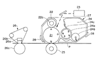
図5は本発明に従う画像形成装置の一例の概略構成模型図である。
この画像形成装置は、転写式電子写真プロセスを利用した現像同時クリーニングプロセス(クリーナーレスシステム)のレーザープリンター(記録装置)である。クリーニングブレードのようにクリーニング部材を有するクリーニングユニットを除去したプロセスカードリッジを有し、現像剤としては磁性一成分系現像剤を使用し、現像剤担持体上の現像剤層と像担持体が非接触となるよう配置される非接触現像の例を示す。
【0238】
21は像担持体としての回転ドラム型OPC感光体であり、矢印の時計方向に一定速度の周速度(プロセススピード)をもって回転駆動される。
22は接触帯電部材としての帯電ローラーである。
帯電ローラー22は感光体21に対して弾性に抗して所定の押圧力で圧接させて配設してある。nは感光体21と帯電ローラー22の当接部である帯電当接部である。帯電ローラー22は感光体21との接触面である帯電当接部nにおいて対向方向(感光体表面の移動方向と逆方向)に回転駆動される。即ち接触帯電部材としての帯電ローラー2の表面は感光体21の表面に対して速度差を持たせてある。また、帯電ローラー22の表面には、塗布量が均一になるように前記導電性微粉末3を塗布している。
【0239】
また帯電ローラー2の芯金22aには帯電バイアス印加電源から直流電圧を帯電バイアスとして印加してある。ここで、感光体21の表面は帯電ローラー22に対する印加電圧とほぼ等しい電位に直接注入帯電方式にて一様に帯電処理される。
23は露光器である。この露光器により回転感光体21の面に目的の画像情報に対応した静電潜像が形成される。24は現像装置である。感光体21の表面の静電潜像はこの現像装置によりトナー画像として現像される。
【0240】
この現像装置24は、非接触型の反転現像装置である。また、感光体21との対向部である現像部a(現像領域部)にて感光体21の回転方向と順方向に一定速度の周速で回転させる。この現像スリーブ24aに弾性ブレード24cで現像剤が薄層にコートされる。現像剤は弾性ブレード24cで現像スリーブ24aに対する層厚が規制され、また電荷が付与される。現像スリーブ24aにコートされた現像剤はスリーブ24aの回転により、感光体21とスリーブ24aの対向部である現像部aに搬送される。また、スリーブ24aには現像バイアス印加電源より現像バイアス電圧が印加される。そして、現像スリーブ24aと感光体21の間aで1成分ジャンピング現像を行なわせる。
【0241】
25は接触転写手段としての転写ローラーであり、感光体1に一定の線圧で圧接させて転写当接部bを形成させてある。この転写当接部bに不図示の給紙部から所定のタイミングで記録媒体としての転写材Pが給紙され、かつ転写ローラー25に転写バイアス印加電源から所定の転写バイアス電圧が印加されることで、感光体21側のトナー像が転写当接部bに給紙された転写材Pの面に順次に転写されていく。
そして、一定のローラ抵抗値のものを用いDC電圧を印加して転写を行なう。即ち、転写当接部bに導入された転写材Pはこの転写当接部bを挟持搬送されて、その表面側に感光体21の表面に形成担持されているトナー画像が順次に静電気力と押圧力にて転写されていく。
【0242】
26は熱定着方式等の定着装置である。転写当接部bに給紙されて感光体21側のトナー像の転写を受けた転写材Pは感光体1の表面から分離されてこの定着装置26に導入され、トナー像の定着を受けて画像形成物(プリント、コピー)として装置外へ排出される。
【0243】
このプリンターはクリーニングユニットを除去しており、転写材Pに対するトナー像転写後の感光体21の表面に残留の転写残トナーはクリーナーで除去されることなく、感光体21の回転にともない帯電部nを経由して現像部aに至り、現像装置24において現像同時クリーニング(回収)される。
【0244】
27はプリンター本体に対して着脱自在の画像形成装置及びプロセスカートリッジである。このプリンターは、感光体21、帯電ローラー22、現像装置24の3つのプロセス機器を一括してプリンター本体に対して着脱自在のプロセスカートリッジとして構成してある。プロセスカートリッジ化するプロセス機器の組み合わせ等は上記に限られるものではなく任意である。例えば、現像装置と感光体の組み合わせ、現像装置と帯電ローラーの組み合わせ、現像装置と感光体と帯電ローラーの組み合わせ等が考えられる。
28はプロセスカートリジの着脱案内・保持部材である。
【0245】
次に、本発明の画像形成方法における導電性微粉末の挙動について以下説明するする。
現像装置24の現像剤tに混入させた導電性微粉末mは、現像装置24による感光体1側の静電潜像のトナー現像時にトナーとともに適当量が感光体1側に移行する。
感光体21上のトナー画像は転写部bにおいて転写バイアスの影響で記録媒体である転写材P側に引かれて積極的に転移するが、感光体21上の導電性微粉末mは導電性であることで転写材P側には積極的には転移せず、感光体1上に実質的に付着保持されて残留する。
【0246】
本発明の一態様においては、画像形成装置はクリーニング工程を有さないため、転写後の感光体1の表面に残存の転写残トナーおよび上記の残存導電性微粉末mは感光体1と接触帯電部材である帯電ローラー22の当接部である帯電部nに感光体21面の移動でそのまま持ち運ばれて、帯電ローラー22に付着または混入する。したがって、感光体21と帯電ローラー22との当接部nにこの導電性微粉末mが存在した状態で感光体21の直接注入帯電が行なわれる。
【0247】
この導電性微粉末mの存在により、帯電ローラー22にトナーが付着・混入した場合でも、帯電ローラー22の感光体21への緻密な接触性と接触抵抗を維持できるため、該帯電ローラー22による感光体21の直接注入帯電を行なわせることができる。
【0248】
つまり、帯電ローラー22が導電性微粉末mを介して密に感光体21に接触して、帯電ローラー22と感光体21の相互接触面に存在する導電性微粉末mが感光体1表面を隙間なく摺擦することで、帯電ローラー22による感光体21の帯電は導電性微粉末mの存在により放電現象を用いない安定かつ安全な直接注入帯電が支配的となり、従来のローラ帯電等では得られなかった高い帯電効率が得られ、帯電ローラー22に印加した電圧とほぼ同等の電位を感光体21に与えることができる。
【0249】
また帯電ローラー22に付着または混入した転写残トナーは帯電ローラー22から徐々に感光体21上に吐き出されて感光体21面の移動とともに現像部に至り、現像手段において現像同時クリーニング(回収)される。
現像同時クリーニングは、転写後に感光体21上に残留したトナーを、引き続く画像形成工程の現像時、即ち引き続き感光体を帯電し、露光して潜像を形成し、該潜像の現像時において、現像装置のかぶり取りバイアス、即ち現像装置に印加する直流電圧と感光体の表面電位間の電位差であるかぶり取り電位差(Vback)によって回収するものである。上記のプリンターのように反転現像の場合では、この現像同時クリーニングは、現像バイアスによる感光体の暗部電位から現像スリーブにトナーを回収する電界と、現像スリーブから感光体の明部電位へトナーを付着させる電界の作用でなされる。
【0250】
また、画像形成装置が稼働されることで、現像装置24の現像剤tに混入させてある導電性微粉末mが現像部aで感光体21面に移行し該像担持面の移動により転写部bを経て帯電部nに持ち運ばれて帯電部nに新しい粒子mが逐次に供給され続けるため、帯電部nにおいて導電性微粉末mが脱落等で減少したり、該粒子mが劣化するなどしても、帯電性の低下が生じることが防止されて良好な帯電性が安定して維持される。
【0251】
このように、接触帯電方式、転写方式、トナーリサイクルプロセスの画像形成装置において、接触帯電部材として簡易な帯電ローラー22を用いて、しかも該帯電ローラー22の転写残トナーによる汚染にかかわらず、低印加電圧でオゾンレスの直接注入帯電を長期に渡り安定に維持させることができ、均一な帯電性を与えることが出来、オゾン生成物による障害、帯電不良による障害等のない、簡易な構成、低コストな画像形成装置を得ることができる。
【0252】
また、前述のように導電性微粉末mは帯電性を損なわないために、電気抵抗値が抵抗値が1×10⁹Ω・cm以下である必要がある。そのため、現像部aにおいて現像剤が直接感光体21に接触する接触現像装置を用いた場合には、現像像剤中の導電性微粉末mを通じて、現像バイアスにより感光体21に電荷注入され、画像かぶりが発生してしまう。
【0253】
しかし、上記の例では現像装置は非接触型現像装置であるので、現像バイアスが感光体21に注入されることがなく、良好な画像を得ることが出来る。また、現像部aにおいて感光体21への電荷注入が生じないため、ACのバイアスなど現像スリーブ24aと感光体21間に高電位差を持たせることが可能であり、導電性微粉末mが均等に現像されやすく、均一に導電性微粉末mを感光体21表面に塗布し、帯電部で均一な接触を行い、良好な帯電性を得ることが出来き、良好な画像を得ることが可能となる。
【0254】
帯電ローラー22と感光体21との接触面nに導電性微粉末mを介在させることにより、該導電性微粉末mの潤滑効果(摩擦低減効果)により帯電ローラー22と感光体21との間に容易に効果的に速度差を設けることが可能となる。
帯電ローラー22と感光体21との間に速度差を設けることにより、帯電ローラー22と感光体21の相互接触面部nにおいて導電性微粉末mが感光体1に接触する機会を格段に増加させ、高い接触性を得ることができ、良好な直接注入帯電を可能としている。
【0255】
上記の例では、帯電ローラー22を回転駆動し、その回転方向は感光体21表面の移動方向とは逆方向に回転するように構成することで、帯電部nに持ち運ばれる感光体21上の転写残トナーを帯電ローラー22に一時的に回収し均す効果を得ている。即ち、逆方向回転で感光体1上の転写残トナーを一旦引離し帯電を行なうことにより優位に直接注入帯電を行なうことが可能である。
更に、この例では像担持体としての感光ドラム21と接触帯電部材としての帯電ローラー22との帯電当接部nにおける適当な量の導電性微粉末mの介在によって、該粒子による潤滑効果により帯電ローラー22と感光ドラム21との摩擦を低減し、帯電ローラー22を感光ドラム21に速度差を持って回転駆動させることが容易である。つまり、駆動トルクが低減し、帯電ローラー22や感光ドラム21の表面の削れ或いは傷を防止できる。更に該粒子による接触機会増加により十分な帯電性能が得られる。また、導電性微粉末の帯電ローラー22からの脱落よる作像上に悪影響もない。
【0256】
【実施例】
以下、本発明を製造例及び実施例により具体的に説明するが、これは本発明をなんら限定するものではない。尚、以下の配合における部数は全て質量部である。
(表面処理磁性体の製造例1)
硫酸第一鉄水溶液中に、鉄イオンに対してl.0〜1.1当量の苛性ソーダ溶液を混合し、水酸化第一鉄を含む水溶液を調製した。
水溶液のpHを9前後に維持しながら、空気を吹き込み、80〜90℃で酸化反応を行い、種晶を生成させるスラリー液を調製した。
【0257】
次いで、このスラリー液に当初のアルカリ量(苛性ソーダのナトリウム成分)に対し0.9〜1.2当量となるよう硫酸第一鉄水溶液を加えた後、スラリー液をpH8に維持して、空気を吹込みながら酸化反応をすすめ、酸化反応後に生成した磁性酸化鉄粒子を洗浄、濾過して一旦取り出した。この時、含水サンプルを少量採取し、含水量を計っておいた。次に、この含水サンプルを乾燥せずに別の水系媒体中に再分散させた後、再分散液のpHを約6に調製し、十分攪拌しながらシランカップリング剤(n−C10H21Si(OCH3)3)を磁性酸化鉄に対し1.0質量部(磁性酸化鉄の量は含水サンプルから含水量を引いた値として計算した)添加し、カップリング処理を行った。生成した疎水性酸化鉄粒子を常法により洗浄、濾過、乾燥し、次いで若干凝集している粒子を解砕処理して、表面処理磁性体1を得た。
【0258】
(磁性体の製造例1)表面処理磁性体の製造例1と同様に酸化反応を進め、酸化反応後に生成した磁性酸化鉄粒子を洗浄、濾過後、表面処理を行わずに、乾燥し、凝集している粒子を解砕処理し磁性体1を得た。
(表面処理磁性体の製造例2)磁性体の製造例1で得られた磁性体1を、別の水系媒体中に再分散させた後、再分散液のpHを約6に調製し、十分攪拌しながらシランカップリング剤(n−C10H21Si(OCH3)3)を磁性酸化鉄に対し1.0質量部添加し、カップリング処理を行った。生成した疎水性酸化鉄粒子を常法により洗浄、濾過、乾燥し、次いで凝集している粒子を解砕処理して、表面処理磁性体2を得た。
(表面処理磁性体の製造例3)表面処置磁性体の製造例1に於いてシランカップリング剤を(n−C6H13Si(OCH3)3)とする以外は同様にして表面処理磁性体3を得た。
(表面処理磁性体の製造例4)表面処置磁性体の製造例1に於いてシランカップリング剤を(n−C18 H 37Si(OCH3)3)とする以外は同様にして表面処理磁性体4を得た。
【0259】
【表1】
体積平均粒径3.7μm、粒度分布における0.5μm以下の割合が6.6体積%で、5μm以上の割合が8個数%の微粒子酸化亜鉛(抵抗値80Ω・cm、一次粒子径0.1〜0.3μmの酸化亜鉛一次粒子を圧力により造粒した得られた物、白色)を導電性微粉末1とする。
この導電性微粉末1は、走査型電子顕微鏡にて3000倍及び3万倍で観察したところ、0.1〜0.3μmの酸化亜鉛一次粒子と1〜10μmの凝集体からなっていた。
実施例1の画像形成装置で画像露光に用いられるレーザービームスキャナの露光光波長740nmにあわせて、波長740nmの光源を用いて、この波長域における透過率をX−Rite社製310T透過型濃度計を用い測定したところ、この導電性微粉末1の透過率はおよそ35%であった。
【0260】
(導電性微粉末2)導電性微粒末1を風力分級して得られた、体積平均粒径2.4μm、粒度分布における0.5μm以下の割合が4.1体積%で、5μm以上の割合が1個数%の微粒子酸化亜鉛(抵抗値440Ω・cm、透過率35%)を導電性微粉末2とする。この導電性微粉末2は、走査型電子顕微鏡にて観察したところ、0.1〜0.3μmの酸化亜鉛一次粒子と1〜5μmの凝集体からなっていたが、導電性微粉末1と比較すると、一次粒子は減少していた。
【0261】
(導電性微粉末3)
導電性微粒末1を風力分級して得られた、体積平均粒径1.5μm、粒度分布における0.5μm以下の割合が35体積%で、5μm以上の割合が0個数%の微粒子酸化亜鉛(抵抗値1500Ω・cm、透過率35%)を導電性微粉末3とする。
この導電性微粉末3は、走査型電子顕微鏡にて観察したところ、0.1〜0.3μmの酸化亜鉛一次粒子と1〜4μmの凝集体からなっていたが、導電性微粉末2と比較すると、一次粒子は増加していた。
(導電性微粉末4)
体積平均粒径0.3μm、粒度分布における0.5μm以下の割合が80体積%、5μm以上の割合が0個数%の微粒子酸化亜鉛(抵抗値100Ω・cm、一次粒子径0.1〜0.3μm、白色、透過率35%、純度99%以上)を導電性微粉末4とする。
この導電性微粉末4は、走査型電子顕微鏡にて観察したところ、凝集体の少ない0.1〜0.3μmの酸化亜鉛一次粒子からなっていた。
(導電性微粉末5)
酸化スズ・アンチモンで表面処理された体積平均粒径2.8μmのホウ酸アルミニウムを風力分級によって粗粒子を除いた後に、水系に分散しての濾過を繰り返し行うことで微粒子を除き、体積平均粒径3.2μm、粒度分布における0.5μm以下の割合が0.4体積%で、5μm以上の割合が1個数%の灰白色の導電性粒子を得た。これを導電性微粉末5とする。
導電性微粉末1〜5の代表的物性値を下記表2に示す。
【0262】
【表2】
イオン交換水709gに0.1M−Na3PO4水溶液451gを投入し60℃に加温した後、1.0M−CaCl2水溶液67.7gを徐々に添加してCa3 (PO4)2を含む水系媒体を得た。
【0263】
スチレン 80部
n−ブチルアクリレート 20部
ビスフェノールAのP.O.及びE.O.付加物とフマル酸の縮合反応により得られる不飽和ポリエステル樹脂 2部
ビスフェノールAのP.O.及びE.O.付加物とテレフタル酸の縮合反応により得られる飽和ポリエステル樹脂 3部
負荷電性制御剤(下記の式に示す
モノアゾ染料系のFe化合物) 1部
【0264】
【化12】
上記処方をアトライター(三井三池化工機(株))を用いて均一に分散混合した。
この単量体組成物を60℃に加温し、そこにベヘニン酸ベヘニルを主体とするエステルワックス(DSCにおける吸熱ピークの極大値72℃)6部を添加混合溶解し、これに重合開始剤2,2’−アゾビス(2,4−ジメチルバレロニトリル)[t1/2 =140分,60℃条件下]5gを溶解した。
前記水系媒体中に上記重合性単量体系を投入し、60℃、N2雰囲気下においてTK式ホモミキサー(特殊機化工業(株))にて10,000rpmで15分間撹拌し、造粒した。その後パドル撹拌翼で撹拌しつつ、60℃で6時間反応させた。その後液温を80℃とし更に4時間撹拌を続けた。反応終了後、80℃で更に2時間蒸留を行い、その後、懸濁液を冷却し、塩酸を加えてCa3(PO4)2 を溶解し、濾過,水洗,乾燥して重量平均粒径6.5μmのトナー粒子を得た。
【0265】
このトナー粒子100部と、導電性微粉末3の2.0部と、一次粒径8nmのシリカにヘキサメチルジシラザンで表面を処理し処理後のBET値が250m2/gの疎水性シリカ微粉体1.2部とをヘンシェルミキサー(三井三池化工機(株))で混合して、一成分系磁性現像剤(磁性トナー)Aを調製した。現像剤Aの物性を表3に示す。
[現像剤の製造例2]現像剤の製造例1と同様の手法により重量平均粒径6.4μmのトナー粒子を得た。このトナー粒子100部と、導電性微粉末3の2.0部と、一次粒径12nmのシリカにヘキサメチルジシラザン処理した後シリコーンオイルで処理し、処理後のBET値が140m2/gの疎水性シリカ微粉体1.2部とをヘンシェルミキサー(三井三池化工機(株))で混合して、一成分系磁性現像剤B(磁性トナー)を調製した。現像剤Bの物性を表3に示す。
【0266】
[現像剤の製造例3]現像剤の製造例1において、Na3PO4水溶液とCaCl2水溶液の投入量を変更し、重量平均粒径3.5μmのトナー粒子を得た。このトナー粒子100部と、現像剤の製造例2で使用した疎水性シリカ微粉体2.0部とをヘンシェルミキサー(三井三池化工機(株))で混合して、一成分系磁性現像剤C(磁性トナー)を調製した。現像剤Cの物性を表3に示す。
[現像剤の製造例4]現像剤の製造例1において、エステルワックスを低分子量ポリエチレン(DSCにおける吸熱ピークの極大値123℃)に変更し、重量平均粒径10.4μmのトナー粒子を得た。このトナー粒子100部と、現像剤の製造例2で使用した疎水性シリカ微粉体1.0部とをヘンシェルミキサー(三井三池化工機(株))で混合して、一成分系磁性現像剤D(磁性トナー)を調製した。現像剤Dの物性を表3に示す。
[現像剤の製造例5]現像剤の製造例1において、エステルワックスの使用量を51部とする以外は同様の手法により、重量平均粒径8.0μmのトナー粒子を得た。このトナー粒子100部と、現像剤の製造例2で使用した疎水性シリカ微粉体1.2部とをヘンシェルミキサー(三井三池化工機(株))で混合して、一成分系磁性現像剤E(磁性トナー)を調製した。現像剤Eの物性を表3に示す。
【0267】
[現像剤の製造例6]
現像剤の製造例1において、エステルワックスの使用量を0.4部とする以外は同様の手法により、重量平均粒径7.5μmのトナー粒子を得た。このトナー粒子100部と、現像剤の製造例2で使用した疎水性シリカ微粉体1.2部とをヘンシェルミキサー(三井三池化工機(株))で混合して、一成分系磁性現像剤F(磁性トナー)を調製した。現像剤Fの物性を表3に示す。
[現像剤の製造例7]
現像剤の製造例1において、表面処理磁性体1の使用量を50部とする以外は同様の手法により、重量平均粒径7.4μmのトナー粒子を得た。このトナー粒子100部と、現像剤の製造例2で使用した疎水性シリカ微粉体1.2部とをヘンシェルミキサー(三井三池化工機(株))で混合して、一成分系磁性現像剤G(磁性トナー)を調製した。現像剤Gの物性を表3に示す。
[現像剤の製造例8]
現像剤の製造例1において、表面処理磁性体1を150部使用する以外は同様の手法により、重量平均粒径7.9μmのトナー粒子を得た。このトナー粒子100部と、現像剤の製造例2で使用した疎水性シリカ微粉体1.2部とをヘンシェルミキサー(三井三池化工機(株))で混合して、一成分系磁性現像剤H(磁性トナー)を調製した。現像剤Hの物性を表3に示す。
【0268】
[現像剤の製造例9]現像剤の製造例1において、表面処理磁性体1に代えて表面処理磁性体2を90部使用する以外は同様の手法により、重量平均粒径7.7μmのトナー粒子を得た。このトナー粒子100部と、現像剤の製造例1で使用したヘキサメチルジシラザンによる表面疎水化処理シリカ微粉体1.2部とをヘンシェルミキサー(三井三池化工機(株))で混合して、一成分系磁性現像剤I(磁性トナー)を調製した。現像剤Iの物性を表3に示す。
[現像剤の製造例10]現像剤の製造例1において、表面処理磁性体1に代えて表面処理磁性体3を90部使用する以外は同様の手法により、重量平均粒径6.9μmのトナー粒子を得た。このトナー粒子100部と、現像剤の製造例2で使用した疎水性シリカ微粉体1.2部とをヘンシェルミキサー(三井三池化工機(株))で混合して、一成分系磁性現像剤J(磁性トナー)を調製した。現像剤Jの物性を表3に示す。
[現像剤の製造例11]現像剤の製造例1において、表面処理磁性体1に代えて表面処理磁性体4を90部使用する以外は同様の手法により、重量平均粒径6.7μmのトナー粒子を得た。このトナー粒子100部と、現像剤の製造例2で使用した疎水性シリカ微粉体1.2部とをヘンシェルミキサー(三井三池化工機(株))で混合して、一成分系磁性現像剤K(磁性トナー)を調製した。現像剤Kの物性を表3に示す。
[現像剤の製造例12〜15]現像剤の製造例2において、導電性微粉末3を導電性微粉末1、2、4、5とする以外は同様にして一成分系磁性現像剤(磁性トナー)L、M、N、Oを調製した。現像剤L、M、N、Oの物性を表3に示す。
【0269】
[現像剤の比較製造例1]
現像剤の製造例1において、表面処理磁性体1に代えて磁性体1を90部使用する以外は同様の手法により、重量平均粒径7.9μmのトナー粒子を得た。このトナー粒子100部と、現像剤の製造例2で使用した疎水性シリカ微粉体1.2部とをヘンシェルミキサー(三井三池化工機(株))で混合して、一成分系磁性現像剤P(磁性トナー)を調製した。
現像剤Pの物性を表3に示す。
[現像剤の比較製造例2]
現像剤の製造例1において、導電性微粉体を添加しない以外は同様にして一成分系磁性現像剤Q(磁性トナー)を調製した。現像剤Qの物性を表3に示す。
[現像剤の比較製造例3]
スチレン/n−ブチルアクリレート共重合体
(重量比80/20) 20部
ビスフェノールAのP.O.及びE.O.付加物とフマル酸の縮合反応により得られる不飽和ポリエステル樹脂 2部
ビスフェノールAのP.O.及びE.O.付加物とテレフタル酸の縮合反応により得られる飽和ポリエステル樹脂 3部
負荷電性制御剤(下記の式に示す
モノアゾ染料系のFe化合物) 4部
【0270】
【化13】
実施例1で用いたエステルワックス 5部
上記材料をブレンダーにて混合し、110℃に加熱した2軸エクストルーダーで溶融混練し、冷却した混練物をハンマーミルで粗粉砕し、粗粉砕物をジェットミルで微粉砕後、得られた微粉砕物を風力分級して重量平均粒径9.3μmのトナー粒子を得た。このトナー粒子100部に対して現像剤の製造例1で使用した疎水性コロイダルシリカ1.0部を加えた混合物をヘンシェルミキサーで混合し一成分系磁性現像剤R(磁性トナー)を調製した。現像剤Rの物性を表3に示す。
【0271】
[現像剤の比較製造例4]
現像剤の比較製造例3において、粗粉砕物をターボミル(ターボ工業社製)で微粉砕する以外は同様の手法により、トナーを得た。その後衝撃式表面処理装置(処理温度50℃、回転式処理ブレード周速90m/sec.)を用いて重量平均粒径8.0μmの球形化トナー粒子を得た。
次に、得られた球形化トナー粒子100部に対して現像剤の製造例2で使用した疎水性コロイダルシリカ1.0部を加えた混合物をヘンシェルミキサーで混合し一成分系磁性現像剤S(磁性トナー)を調製した。現像剤Sの物性を表3に示す。得られた磁性現像剤の磁場79.6kA/mにおける磁化の強さは、現像剤Gは18.9、現像剤Hは35.0、であり、他のの現像剤はいずれも26〜30Am2/kgであった。
【0272】
【表3】
感光体としては30φのAlシリンダーを基体とした。これに、図3に示すような構成の層を順次浸漬塗布により積層して、感光体を作成した。
(1)導電性被覆層:酸化錫及び酸化チタンの粉末をフェノール樹脂に分散したものを主体とする。膜厚15μm。
(2)下引き層:変性ナイロン、及び共重合ナイロンを主体とする。膜厚0.6μm。
(3)電荷発生層:長波長域に吸収を持つアゾ顔料をブチラール樹脂に分散したものを主体とする。膜厚0.6μm。
(4)電荷輸送層:ホール搬送性トリフェニルアミン 化合物をポリカーボネート樹脂(オストワルド粘度法による分子量2万)に8:10の質量比で溶解したものを主体とし、さらにポリ4フッ化エチレン粉体(粒径0.2μm)を総固形分に対して10質量%添加し、均一に分散した。膜厚25μm。水に対する接触角は95度であった。
なお、接触角の測定は、純水を用い、装置は、協和界面科学(株)、接触角計CA−X型を用いた。
【0273】
【表3】
感光ドラムと現像スリーブとの間隙は290μmとし、トナー担持体として下記の構成の層厚約7μm、JIS中心線平均粗さ(Ra)1.0μmの樹脂層を、表面をブラストした直径16φのアルミニウム円筒上に形成した現像スリーブを使用し、現像磁極85mT(850ガウス)、トナー規制部材として厚み1.0mm、自由長1.0mmのシリコーンゴム製ブレードを29.4N/m(30g/cm)の線圧で当接させた。
【0275】
フェノール樹脂 100部
グラファイト(体積平均粒径約7μm) 90部
カーボンブラック 10部
次いで、現像バイアスとして直流バイアス成分Vdc=−500V、重畳する交流バイアス成分Vp−p=1600V、f=2000Hzを用いた。また、現像スリーブの周速は感光体周速(94mm/sec)に対して順方向に110%のスピード(103mm/sec)とした。
また、図4のような転写ローラー(導電性カーボンを分散したエチレン−プロピレンゴム製、導電性弾性層の体積抵抗値108Ωcm、表面ゴム硬度24゜、直径20mm、当接圧59 N/m(60g/cm))を図4中A方向の感光体周速(94mm/sec)に対して等速とし、転写バイアスは直流1.5kVとした。定着方法としてはLBP−1760のオイル塗布機能のない、フィルムを介してヒーターにより加熱加圧定着する方式の定着装置を用いた。この時、加圧ローラはフッ素系樹脂の表面層を有するものを使用し、ローラの直径は30mmであった。また、定着温度は180℃、ニップ幅を7mmに設定した。
まず、現像剤として現像剤Aを使用し、15℃、10%RH環境下において画出し試験を行った。転写材としては90g/m2の紙を使用した。その結果、初期において高い転写性を示し、文字やラインの転写中抜けもなく、非画像へのカブリのない良好な画像が得られた。
【0276】
次に、印字面積比率5%の横ラインのみからなる画像パターンで耐久性の評価を行った。画像評価は以下のように行った。
ページ内画像濃度むらはべた黒の先端と後端の平均マクベス濃度差とした。
また、感光体の削れ及びトナー融着の評価は、画像不良が現れやすいハーフトーン画像上に、削れあるいはトナー融着による画像不良、即ち黒点あるいは白抜けが発生した耐久枚数で判断した。発生するまでの耐久枚数が多い程、画像形成方法の耐久性が良好なことを意味する。加えて、転写残トナーによる一次帯電不良に起因する画像不良、即ち帯電ムラもハーフトーン画像上で評価した。
【0277】
転写効率は、ベタ黒画像転写後の感光体上の転写残トナーをマイラーテープによりテーピングしてはぎ取り、紙上に貼ったもののマクベス濃度の値をC、転写後定着前のトナーの載った紙上にマイラーテープを貼ったもののマクベス濃度をD、未使用の紙上に貼ったマイラーテープのマクベス濃度をEとした時、近似的に以下の式で計算した。
【0278】
【数7】
転写効率(%)=(D−C/D−E)×100
転写効率は90%以上であれば問題の無い画像である。
また、耐久初期の解像力は、潜像電界によって電界が閉じやすく、再現しにくい600dpiにおける小径孤立1ドットの再現性によって評価した。
【0279】
◎ 非常に良好 :100個中の欠損が5個以下
○ 良好 :100個中の欠損が6−10個
△ 実用可 :100個中の欠損が11−20個
× 実用不可 :100個中の欠損が20個以上
カブリの測定は、東京電色社製のREFLECTMETER MODEL TC−6DSを使用して測定した。フィルターは、グリーンフィルターを用いた。ドラム上カブリはべた白画像の転写前ドラム上をマイラーテープでテーピングし、紙上にマイラーテープを貼ったものの反射率から、未使用の紙上に貼ったマイラーテープのマクベス濃度を差し引いて算出した。
また定着後カブリはやはりべた白画像で下記の式より算出した。
【0280】
【数8】
画像濃度はマクベス濃度計RD918(マクベス社製)で測定した。
初期濃度は画だし20枚目の濃度とした。
定着オフセット性は、初期から耐久100枚までの画像サンプルの裏側に発生する汚れを観察し、発生枚数を数えた。
得られた結果を表4に示す。
【0281】
(実施例2)
現像剤として現像剤Bを使用し、実施例1と同様の画像形成方法で画出し試験を行ったところ、表4に示した様に非常に良好な結果が得られた。
(実施例3〜11)
現像剤として現像剤C、D、E、F、G、H、I、J、Kを使用し、実施例1と同様の画像形成方法で画出し試験を行った。その結果、表4に示した様に実用的に問題の無い結果が得られた。
(実施例12〜15)
現像剤として現像剤L、M、N、Oを使用し、実施例1と同様の画像形成方法で画出し試験を行った。その結果、表4に示した様に実用的に問題の無い結果が得られた。
【0282】
(比較例1)
現像剤として現像剤Pを使用し、実施例1と同様の画像形成方法で画出し試験を行った。その結果、初期から非常に画像濃度が低く実用に耐えるものではなかった。結果を表4に示す。
(比較例2)
現像剤として現像剤Qを使用し、実施例1と同様の画像形成方法で画出し試験を行った。その結果、画像濃度がやや低く、ページ内濃度むらの大きな画像となった。結果を表4に示す。
(比較例3)
現像剤として現像剤Rを使用し、実施例1と同様の画像形成方法で画出し試験を行った。その結果、初期からやや画像濃度の薄いチャージアップした画像となった。結果を表4に示す。
(比較例4)
現像剤として現像剤Sを使用し、実施例1と同様の画像形成方法で画出し試験を行った。その結果、比較例3に比べてもさらに画像濃度が低い画像となった。結果を表4に示す。
【0283】
【表4】
以下、具体的実施例によって本発明を説明するが本発明はなんらこれに限定されるものではない。
まず、本発明の実施例に用いる像担持体としての感光体の製造例について述べる。
【0284】
(感光体製造例2)
感光体は負帯電用の有機光導電性物質を用いた感光体(以下OPC感光体)であり、φ30mmのアルミニウム製のシリンダーを基体とした。これに、図8に示すような構成の層を順次浸漬塗布により積層して、感光体を作成した。
第1層は導電層であり、アルミニウムシリンダーの欠陥等をならすため、またレーザ露光の反射によるモアレの発生を防止するために設けられている厚さ約20μmの導電性粒子分散樹脂層(酸化錫及び酸化チタンの粉末をフェノール樹脂に分散したものを主体とする)である。
第2層は正電荷注入防止層(下引き層)であり、アルミニウム支持体から注入された正電荷が感光体表面に帯電された負電荷を打ち消すのを防止する役割を果し、メトキシメチル化ナイロンによって106Ω・cm程度に抵抗調整された厚さ約1μmの中抵抗層である。
第3層は電荷発生層であり、ジスアゾ系の顔料をブチラール樹脂に分散した厚さ約0.3μmの層であり、レーザ露光を受けることによって正負の電荷対を発生する。
第4層は電荷輸送層であり、ポリカーボネート樹脂にヒドラゾン化合物を分散した厚さ約25μmの層であり、P型半導体である。従って、感光体表面に帯電された負電荷はこの層を移動することはできず、電荷発生層で発生した正電荷のみを感光体表面に輸送することができる。
第5層は電荷注入層であり、光硬化性のアクリル樹脂に導電性酸化スズ超微粒子及び粒径約0.25μmの四フッ化エチレン樹脂粒子を分散したものである。具体的には、アンチモンをドーピングし低抵抗化した粒径約0.03μmの酸化スズ粒子を樹脂に対して100重量%、更に四フッ化エチレン樹脂粒子を20重量%、分散剤を1.2重量%分散したものである。このようにして調製した塗工液をスプレー塗工法にて厚さ約2.5μmに塗工して電荷注入層とした。
得られた感光体の表面の抵抗値は、5×10¹²Ω・cm、感光体表面の水に対する接触角は、102度であった。
【0285】
(感光体製造例3)
感光体製造例2の第5層に、四フッ化エチレン樹脂粒子と分散剤を分散しなかったこと以外は、感光体製造例2と同様にして感光体を作成した。これにより、感光体表面層の体積抵抗値は、2×10¹²Ω・cm、感光体表面の水に対する接触角は、78度であった。
(感光体製造例4)
感光体製造例2の第5層において、アンチモンをド−ピングし、低抵抗化した粒径約0.03μmの酸化スズ粒子を光硬化性のアクリル樹脂100質量部に対して300質量部分散したものを加えたこと以外は、感光体製造例2と同様にして感光体を作成した。この場合、感光体表面層の体積抵抗値は、2×10⁷Ω・cm、感光体表面の水に対する接触角は、88度であった。
(感光体製造例5)
感光体製造例2の第5層(電荷注入層)を設けない、電荷輸送層を最外層とする4層構成の感光体とすること以外は、感光体製造例2と同様にして感光体を作成した。この場合、感光体表面層の体積抵抗値は、1×10¹⁵Ω・cm、感光体表面の水に対する接触角は、73度であった。
【0286】
次に、本発明の実施例に用いる帯電部材の製造例について述べる。
(帯電部材の製造例1)
6φ、264mmのSUSローラーを芯金とし、芯金上にウレタン樹脂、導電性粒子としてのカーボンブラック、硫化剤、発泡剤等を処方した中抵抗の発泡ウレタン層をローラ状に形成し、さらに切削研磨し形状及び表面性を整え、可撓性部材として12φ、234mmの帯電ローラーを作成した。
得られた帯電ローラーは、抵抗値が105Ω・cmであり、硬度は、アスカーC硬度で30度であった。
また、この帯電ローラー表面を走査型電子顕微鏡で観察したところ、平均セル径は約100μmで、空隙率は60%であった。
【0287】
(帯電部材の製造例2)
6φ、264mmのSUSローラーを芯金とし、芯金上に導電性ナイロン繊維をパイル地にしたテープを金属製の芯金にスパイラル状に巻き付けてロール状帯電ブラシを作成した。ナイロン繊維にカーボンブラックを分散させて抵抗調整された、繊維の太さが6デニール(300デニール/50フィラメント)、ブラシの繊維の長さは3mm、ブラシ密度は1平方インチ当たり10万本で植毛された物を用いた。得られた帯電ブラシロールの抵抗値は1×107Ω・cmであった。
【0288】
(実施例16)(図5)
図5は本発明に従う画像形成装置の一例の概略構成模型図である。
実施例1本例の画像形成装置は、転写式電子写真プロセスを利用した現像同時クリーニングプロセス(クリーナーレスシステム)のレーザープリンター(記録装置)である。クリーニングブレードの如きクリーニング部材を有するクリーニングユニットを除去したプロセスカードリッジを有し、現像剤としては磁性一成分系現像剤を使用し、現像剤担持体上の現像剤層と像担持体が非接触となるよう配置される非接触現像の例である。
【0289】
(a)本例プリンターの全体的な概略構成
21は像担持体としての、感光体製造例2の回転ドラム型OPC感光体であり、矢印の時計方向に94mm/secの周速度(プロセススピード)をもって回転駆動される。
22は接触帯電部材としての帯電部材製造例1の帯電ローラーである。
帯電ローラー22は感光体21に対して弾性に抗して所定の押圧力で圧接させて配設してある。nは感光体21と帯電ローラー22の当接部である帯電当接部である。本例では、帯電ローラー22は感光体21との接触面である帯電当接部nにおいて対向方向(感光体表面の移動方向と逆方向)に100%の周速で回転駆動されている。即ち接触帯電部材としての帯電ローラー2の表面は感光体21の表面に対して相対移動速度比200%の相対速度差を有している。また、帯電ローラー22の表面には、塗布量がおよそ1×10⁴個/mm2で均一になるように前記導電性微粉末3を塗布した。
【0290】
また帯電ローラー2の芯金22aには帯電バイアス印加電源から−700Vの直流電圧を帯電バイアスとして印加するようにした。本例では感光体21の表面は帯電ローラー22に対する印加電圧とほぼ等しい電位(−680V)に直接注入帯電方式にて一様に帯電処理される。これについては後述する。
【0291】
23はレーザーダイオード・ポリゴンミラー等を含むレーザービームスキャナ(露光器)である。このレーザービームスキャナは目的の画像情報の時系列電気ディジタル画素信号に対応して強度変調されたレーザー光を出力し、該レーザー光で上記感光体1の一様帯電面を走査露光Lする。この走査露光Lにより回転感光体21の面に目的の画像情報に対応した静電潜像が形成される。
【0292】
24は現像装置である。感光体21の表面の静電潜像はこの現像装置によりトナー画像として現像される。
本例の現像装置24は、現像剤として現像剤製造例2の負帯電性磁性1成分絶縁現像剤Bを用いた、非接触型の反転現像装置である。現像剤Bには導電性微粉末を外添添加してある。
感光ドラム21と現像スリーブ24aとの間隙は290μmとし、トナー担持体24aとして下記の構成の層厚約7μm、JIS中心線平均粗さ(Ra)1.0μmの樹脂層を、表面をブラストした直径16φのアルミニウム円筒上に形成した現像スリーブを使用し、現像磁極90mT(900ガウス)のマグネットロールを内包し、トナー規制部材として厚み1.0mm、自由長1.5mmのウレタン製ブレードを29.4N/m(30g/cm)の線圧で当接させた。
【0293】
フェノール樹脂 100部
グラファイト(体積平均粒径約7μm) 90部
カーボンブラック 10部
また、感光体21との対向部である現像部a(現像領域部)にて感光体21の回転方向と順方向に感光体21の周速の120%の周速で回転させる。
この現像スリーブ24aに弾性ブレード24cで現像剤が薄層にコートされる。現像剤は弾性ブレード24cで現像スリーブ24aに対する層厚が規制され、また電荷が付与される。この時、現像スリーブ24aにコートされた現像剤量は、15g/m2であった。
現像スリーブ24aにコートされた現像剤はスリーブ24aの回転により、感光体21とスリーブ24aの対向部である現像部aに搬送される。
また、スリーブ24aには現像バイアス印加電源より現像バイアス電圧が印加される。現像バイアス電圧は、−420VのDC電圧と、周波数1600Hz、ピーク間電圧1500V(電界強度5×10⁶V/m)の矩形のAC電圧を重畳したものを用い、現像スリーブ24aと感光体21の間aで1成分ジャンピング現像を行なわせた。
【0294】
25は接触転写手段としての中抵抗の転写ローラーであり、感光体1に98N/m(100g/cm)の線圧で圧接させて転写当接部bを形成させてある。この転写当接部bに不図示の給紙部から所定のタイミングで記録媒体としての転写材Pが給紙され、かつ転写ローラー25に転写バイアス印加電源から所定の転写バイアス電圧が印加されることで、感光体21側のトナー像が転写当接部bに給紙された転写材Pの面に順次に転写されていく。
本例ではローラ抵抗値は5×10⁸Ωcmのものを用い、+3000VのDC電圧を印加して転写を行なった。即ち、転写当接部bに導入された転写材Pはこの転写当接部bを挟持搬送されて、その表面側に感光体21の表面に形成担持されているトナー画像が順次に静電気力と押圧力にて転写されていく。
【0295】
26は熱定着方式等の定着装置である。転写当接部bに給紙されて感光体21側のトナー像の転写を受けた転写材Pは感光体1の表面から分離されてこの定着装置26に導入され、トナー像の定着を受けて画像形成物(プリント、コピー)として装置外へ排出される。
本例のプリンターはクリーニングユニットを除去しており、転写材Pに対するトナー像転写後の感光体21の表面に残留の転写残トナーはクリーナーで除去されることなく、感光体21の回転にともない帯電部nを経由して現像部aに至り、現像装置24において現像同時クリーニング(回収)される。
27はプリンター本体に対して着脱自在の画像形成装置及びプロセスカートリッジである。本例のプリンターは、感光体21、帯電ローラー22、現像装置24の3つのプロセス機器を一括してプリンター本体に対して着脱自在の画像形成装置及びプロセスカートリッジとして構成してある。
28はプロセスカートリジの着脱案内・保持部材である。
【0296】
(b)評価
本実施例では、トナーカートリッジ内に120gの現像剤Bを充填して、2%カバレッジの3000枚の間欠プリントにより、トナーカートリッジ内で現像剤量が少なくなるまで使用した。転写材としては75g/m2のA4コピー紙を用い、一枚間欠で1000枚のプリントを行ったが現像性の低下は見られなかった。また、3000枚の間欠プリント後、帯電ローラー22上で感光体21との当接部nに対応する部分をテーピングし、観察したところ、微量の転写残トナーが確認されるものの、ほぼ白色の酸化亜鉛粒子(導電性微粉末3)で覆われており、介在量はおよそ3×105個/mm2であった。帯電部材と像担持体との当接部に介在している転写残トナーを走査型顕微鏡で観察したところ、表面を非常に粒径が細かい導電性微粉末で固着しているように覆われたような転写残トナーは観察されなかった。
【0297】
また、感光体21と帯電ローラー22との当接部nに導電性微粉末mが存在した状態で、かつ導電性微粉の抵抗値が1500Ω・cm と十分に低いために、初期より3000枚の間欠プリント後まで帯電不良に起因する画像欠陥を生じず、良好な直接注入帯電性が得られた。
また、像担持体として感光体製造例2の最表面層の体積抵抗値が5×10¹²Ω・cmの感光体を用いたことにより、静電潜像を維持することでシャープな輪郭の文字画像が得られ、3000枚の間欠プリント後も十分な帯電性が得られる直接注入帯電を実現ができる。3000枚の間欠プリント後の直接注入帯電後感光体電位は、印加帯電バイアス−700Vに対して−670Vであり、初期からの帯電性の低下は10Vと軽微であり、帯電性の低下による画像品質の低下は認められなかった。
【0298】
更に、像担持体の表面の水に対する接触角が102度である感光体製造例2の感光体を用いたこととあいまって、転写効率は初期及び3000枚の間欠プリント後も非常に優れていた。転写後の感光体上に転写残トナー量が少ないことを勘案しても、3000枚の間欠プリント後の帯電ローラー2上での転写残トナーが微量であったことと非画像部のカブリが少ないことより、現像での転写残トナーの回収性が良好であったことが解る。更に、3000枚の間欠プリント後も感光体上の傷は軽微であり、この傷に対応して画像上に生じる画像欠陥は実用上許容できるレベルに抑制されていた。
【0299】
以下プリント画像の評価法について述べる。
(1)画像濃度
初期及び3000枚の間欠プリントアウトを終了した後、2日放置して再び電源を入れた1枚目の画像濃度により評価した。尚、画像濃度は「マクベス反射濃度計」(マクベス社製)を用いて、原稿濃度が0.00の白地部分のプリントアウト画像に対する相対濃度を測定した。
【0300】
(2)画像カブリ
「リフレクトメータ」(東京電色社製)により測定したプリントアウト画像の白地部分の白色度と転写紙の白色度の差から、カブリ濃度(%)を算出し、画像カブリを評価した。
【0301】
A:非常に良好(1.5%未満)
B:良好(1.5%以上乃至2.5%未満)
C:普通(2.5%以上乃至4.0%未満)
D:悪い(4%以上)
(3)転写性
転写性はベタ黒画像形成時の感光体上の転写残トナーを、マイラーテープによりテーピングしてはぎ取り、はぎ取ったマイラーテープを紙上に貼ったもののマクベス濃度から、マイラーテープのみを紙上に貼ったもののマクベス濃度を差し引いた数値で評価した。
【0302】
A:非常に良好(0.05未満)
B:良好(0.05以上乃至0.1未満)
C:普通(0.1以上乃至0.2未満)
D:悪い(0.2以上)
(4)帯電性
初期及びプリントアウト試験終了後、一様帯電後の感光体表面電位を現像器位置にセンサーを配置し測定し、その差分により帯電性を評価した。差分がマイナスに大きくなるほど帯電性の低下が大きいことを示す。
(5)像担持体と接触帯電部材との当接部における導電性微粉末の介在量
感光体と接触帯電部材との当接部における導電性微粉末の介在量を前述の方法で測定した。104〜5×10⁵個/mm2の介在量が好ましい。
(6)感光体傷
プリントアウト試験終了後、感光体ドラム表面の傷及び傷へのトナーの固着の発生状況とプリントアウト画像への影響を目視で評価した。
【0303】
A:非常に良好(未発生)
B:良好(わずかに傷の発生が見られるが、画像への影響はない)
C:普通(トナー固着や傷があるが、画像への影響は少ない)
D:悪い(傷に沿ってトナー固着が多く、縦スジ状の画像欠陥を生じる)
(実施例17〜19)
実施例16で用いた感光体製造例2の感光体の代わりに、感光体製造例3〜5で得られた感光体を用いる以外は、実施例16と同様に画出しテストを行った。結果を表5に示す。
感光体製造例3を用いた実施例17では、実施例16と比較するとやや転写性に劣るものの良好な画像が得られた。
感光体製造例4を用いた実施例18では、実施例16と比較するとややトナー画像の輪郭のシャープさが劣るが、それ以外はほぼ良好な性能を示した。
感光体製造例5を用いた実施例19では、実施例16と比較すると初期から帯電効率が悪く、印加帯電バイアス電源−700Vに対し帯電後の感光体表面電位は初期から−660Vとやや劣った。また、3000枚の間欠プリントアウトを終了した後の感光体の傷が実施例1よりも広い範囲でかつ深く入っていた。
【0304】
(実施例20)
実施例16で用いた帯電部材製造例1の帯電部材の代わりに、帯電部材製造例2で得られたブラシ帯電部材を用いる以外は、実施例16と同様に画出しテストを行った。(図6)結果を表5に示す。
実施例16と比較すると感光体と接触帯電部材との当接部における導電性微粉末の介在量がやや少なく、帯電均一性に劣るものの良好な画像が得られた。
【0305】
(実施例21〜23)
実施例16で用いた現像剤Bの代わりに、表3に示す現像剤A、J又はKを用いる以外は、実施例16と同様に画出しテストを行った。結果を表5に示す。
(実施例24〜27)
実施例16で用いた現像剤Bの代わりに現像剤L,M,N,Oを用いる以外は実施例16と同様に行った。結果を表5に示す。
【0306】
(比較例5及び6)
実施例1で用いた現像剤Bの代わりに、表3に示す現像剤P又はQを用いる以外は、実施例1と同様に画出しテストを行った。結果を表5に示す。
現像剤Pを用いた比較例5は、実施例12と比較すると初期から画像濃度がやや薄く、カブリや転写残トナーも非常に多く許容できない画像であった。また、100枚の間欠プリントで帯電ローラがトナーで汚染され、著しい帯電不良が生じた。
現像剤Qを用いた比較例6は、実施例12と比較すると初期から画像濃度が明らかに低くかった、許容できない画像であった。また、3000枚の間欠プリントで更に濃度が低下すると同時に、ドラム上カブリや転写残が徐々に増加し、プリント終了後の帯電部材表面には転写残トナーの付着が多く、帯電部材と像担持体との当接部における導電性微粉末の介在量は明らかに少なく、帯電性は大幅に低下した。
【0307】
【表5】
【発明の効果】
本発明によれば、無機微粉体と導電性微粉体とを表面に有する、磁性体が実質的に表面に露出しておらず、平均円形度が0.970以上で、好ましくはモード円形度が0.990以上である特殊な現像剤を用いることにより、高品位で解像性の高く、カブリや転写性の優れる画像が得られる。
また、本発明の現像剤を用いて接触帯電方法及び磁性一成分現像方法から成る画像形成方法、及び接触帯電方式、当接転写方式、トナーリサイクルプロセスの画像形成装置において、接触帯電部材への転写残トナーへの付着・混入による帯電阻害に打ち勝って像担持体の帯電を良好に行なわせ、長期にわたる繰り返し使用においても、トナーカートリッジ内で現像剤量が少なくなるまで使用された際においても良好な画像を安定して得ることができる。
【0309】
また、接触帯電部材として簡易な部材を用いて、接触帯電部材の転写残トナーによる汚染にかかわらず、低印加電圧でオゾンレスの直接注入帯電を長期にわたり安定に維持させることができ、均一な帯電性を与えることが出来、オゾン生成物による障害、帯電不良による障害等のない、簡易な構成、低コストな画像形成装置及びプロセスカートリッジを得ることができる。
更に、長期の繰り返し使用にわたり、導電性微粉末を帯電部材と像担持体との当接部に介在させることによる像担持体上の傷を大幅に減少でき、画像上の画像欠陥を抑制することができる。
【図面の簡単な説明】
【図1】本発明の実施例に用いた画像形成装置の一例を示す図である。
【図2】一成分現像用現像器の一例を示す図である。
【図3】本発明に用いる感光体の構成の一例を示す図である。
【図4】接触転写部材の一例を示す図である。
【図5】本発明の一態様における画像形成装置の概略構成図である。
【図6】本発明の一態様における画像形成装置の概略構成図である。
【図7】帯電特性グラフである。
【図8】感光体の層構成模型図である。
【符号の説明】
11 アルミ基体
12 導電層
13 注入防止層
14 電荷発生層
15 電荷輸送層
16 電荷注入層
16a 導電粒子(導電フィラー)
21 感光体
22 帯電部材
22a 芯金
23 レーザービームスキャナー(潜像形成手段、露光装置)
24 現像装置
24a 現像スリーブ(現像剤担持体)
24b 攪拌部材
24c 弾性ブレード(層規制部材)
25 転写ローラ
26 定着装置
26a ヒータ
26b 定着フィルム
26c 加圧ローラ
27 プロセスカートリッジ
28 カートリッジ保持部材
34a 芯金
34b 弾性層
100 感光体(像担持体、被帯電体)
102 現像スリーブ(現像剤担持体)
103 弾性ブレード(層規制部材)
104 マグネットローラ
114 転写ローラ(転写部材)
116 クリーナー
117 帯電ローラ(接触帯電部材)
121 レーザービームスキャナー(潜像形成手段、露光装置)
124 給紙ローラ
125 搬送部材
126 定着装置
140 現像装置
141 攪拌部材[0001]
BACKGROUND OF THE INVENTION
The present invention relates to a toner for developing an electrostatic latent image in an image forming method such as an electrophotographic method, an electrostatic recording method, a magnetic recording method, and a toner jet method, and an image forming method using the toner.
[0002]
[Prior art]
Conventionally, many proposals have been made regarding magnetic toners and image forming methods.
U.S. Pat. No. 3,909,258 proposes a developing method using electrically conductive magnetic toner. In this method, a conductive magnetic toner is supported on a cylindrical conductive sleeve having magnetism inside, and this is brought into contact with an electrostatic image for development. At this time, a conductive path is formed by toner particles between the surface of the recording member and the sleeve surface in the developing unit, and electric charges are guided from the sleeve to the toner particles through this conductive path, and between the image part of the electrostatic image. The toner particles adhere to the image area and are developed by the Coulomb force. The developing method using the conductive magnetic toner is an excellent method that avoids the problems associated with the conventional two-component developing method. However, since the toner is conductive, the developed image is transferred from the recording medium to plain paper or the like. There is a problem that it is difficult to electrostatically transfer to the final support member.
[0003]
As a developing method using a high-resistance magnetic toner that can be electrostatically transferred, there is a developing method using dielectric polarization of toner particles. However, this method has problems such as a slow development speed and insufficient density of the developed image, and is difficult in practical use.
[0004]
As another developing method using a high-resistance insulating magnetic toner, the toner particles are frictionally charged by friction between the toner particles, friction between the toner particles and the sleeve, and the like, and then contact the electrostatic image holding member. A developing method is known. However, this method requires less contact between the toner particles and the friction member, and the magnetic toner used has a large amount of magnetic material exposed on the surface of the toner particles. There were problems such as.
[0005]
Furthermore, a jumping development method is proposed in Japanese Patent Application Laid-Open No. 55-18656. This involves applying a very thin magnetic toner on the sleeve, tribocharging it, and then developing it very close to the electrostatic image. This method is an excellent method in that the magnetic toner is thinly applied on the sleeve, thereby increasing the chance of contact between the sleeve and the toner and enabling sufficient frictional charging.
However, the developing method using the insulating magnetic toner has unstable elements related to the insulating magnetic toner to be used. This is because a considerable amount of fine powdery magnetic material is mixed and dispersed in the insulating magnetic toner, and a part of the magnetic material is exposed on the surface of the toner particles. As a result, various characteristics required for the magnetic toner, such as development characteristics and durability of the magnetic toner, are changed or deteriorated.
[0006]
When the magnetic toner containing the conventional magnetic body is used, the above-mentioned problem occurs because the magnetic body is exposed on the surface of the magnetic toner. That is, by exposing magnetic fine particles having a relatively low resistance compared to the resin constituting the toner to the surface of the magnetic toner, the toner charging performance is lowered, the toner fluidity is lowered, and a long-term In use, toner deterioration such as a decrease in image density due to peeling of the magnetic material due to rubbing between the toners or the regulating member, or generation of shading unevenness called sleeve ghost is caused.
Conventionally, proposals regarding magnetic iron oxide contained in a magnetic toner have been made, but there are still points to be improved.
[0007]
For example, JP-A-62-279352 proposes a magnetic toner containing magnetic iron oxide containing silicon element. Such magnetic iron oxide intentionally has silicon element present inside the magnetic iron oxide, but still has a point to be improved in the fluidity of the magnetic toner containing the magnetic iron oxide.
In Japanese Patent Publication No. 3-9045, there is a proposal to control the shape of magnetic iron oxide to be spherical by adding silicate. The magnetic iron oxide obtained by this method uses silicate to control the particle shape, so that a large amount of silicon element is distributed inside the magnetic iron oxide, and the amount of silicon element present on the magnetic iron oxide surface is small. Since the smoothness of the magnetic iron oxide is high, the fluidity of the magnetic toner is improved to some extent, but the adhesion between the binder resin constituting the magnetic toner and the magnetic iron oxide is insufficient.
Japanese Patent Laid-Open No. 61-34070 proposes a method for producing ferric tetroxide by adding a hydrosilicate silicate solution during the oxidation reaction to triiron tetroxide. Although the iron tetroxide by this method has Si element near the surface, the Si element exists in a layer near the iron tetroxide surface, and the surface is weak against mechanical impact such as friction. Has a point.
[0008]
On the other hand, the toner is manufactured as a toner having a desired particle size by melting and mixing a binder resin, a colorant, and the like, uniformly dispersing, pulverizing with a fine pulverizer, and classifying with a classifier (pulverization method). However, there is a limit to the range of materials that can be used to reduce the particle size of the toner. For example, the resin colorant dispersion must be sufficiently brittle and capable of being finely pulverized by an economically usable production apparatus. From this requirement, in order to make the resin colorant dispersion brittle, when the resin colorant dispersion is actually finely pulverized at a high speed, particles having a wide particle size range are easily formed, and in particular, a relatively large proportion of fine particles ( There arises a problem that excessively pulverized particles) are included therein. Further, such highly brittle materials are often further pulverized or powdered when used as developing toners in copying machines and the like.
Also, in the pulverization method, it is difficult to completely disperse solid fine particles such as magnetic powder or colorant in the resin, and depending on the degree of dispersion, it may cause an increase in fog and a decrease in image density. . Furthermore, the pulverization method inherently exposes the magnetic iron oxide particles on the surface of the toner, so that problems still remain in the fluidity of the toner and the charging stability in a harsh environment.
That is, in the pulverization method, there is a limit to the finer toner particles required for high definition and high image quality, and accordingly, the powder characteristics, particularly the uniform chargeability and fluidity of the toner are remarkably attenuated.
[0009]
In order to overcome the problems of the toner by the pulverization method as described above, and further to satisfy the above-described requirements, a toner production method by a suspension polymerization method has been proposed.
Suspension-polymerized toner (hereinafter abbreviated as “polymerized toner”) can easily be finely divided into toner particles. Furthermore, since the resulting toner has a spherical shape, it has excellent fluidity and high image quality. It will be advantageous.
However, when the polymerized toner contains a magnetic substance, its fluidity and charging characteristics are significantly lowered. This is because magnetic particles are generally hydrophilic and thus easily exist on the toner surface. In order to solve this problem, it is important to modify the surface characteristics of the magnetic material.
[0010]
Many proposals have been made regarding surface modification for improving the dispersibility of a magnetic substance in a polymerized toner. For example, various silane coupling agent treatment techniques for magnetic materials are disclosed in Japanese Patent Application Laid-Open Nos. 59-200254, 59-2000025, 59-200277, and 59-224102. Japanese Laid-Open Patent Publication Nos. 63-250660 and 10-239897 disclose techniques for treating silicon element-containing magnetic particles with a silane coupling agent.
However, although the dispersibility in the toner is improved to some extent by these treatments, there is a problem that it is difficult to uniformly hydrophobize the surface of the magnetic material. The generation of non-magnetic particles cannot be avoided, and this is insufficient to improve the dispersibility in the toner to a good level.
[0011]
Also, LED and LBP printers are the mainstream in the recent market as printer devices, and the direction of technology is higher resolution, that is, what was conventionally 240, 300 dpi is 400, 600, 800 dpi. Accordingly, the development method is also required to have higher definition. In addition, copying machines are becoming more sophisticated, and thus are moving toward digitalization. Since this method is mainly a method of forming an electrostatic charge image with a laser, it is also proceeding in the direction of high resolution. In this case as well, a high-resolution and high-definition developing method has been demanded, as in the case of a printer. Japanese Patent Laid-Open Nos. 1-112253 and 2-284158 propose toners having a small particle diameter. The various problems described above have not been sufficiently solved.
[0012]
Further, as a toner for developing a latent image, a two-component developer composed of a carrier and a toner, and a one-component toner (magnetic toner, non-magnetic toner) that does not require a carrier are known. In the two-component system, the toner is charged mainly by friction between the carrier and the toner. In the one-component system, the toner is charged mainly by friction between the toner and the charge imparting member. In addition, as toner, toner and toner are used regardless of the difference between the two-component system and the one-component system.ofA method of adding inorganic fine particles as external additives to toner base particles has been proposed and widely used for the purpose of improving flow characteristics, charging characteristics, and the like. For example, inorganic fine particles hydrophobized in JP-A-5-66608, JP-A-4-9860, etc., or inorganic fine particles that have been hydrophobized and then treated with silicone oil or the like are added. No. 249059, JP-A-4-264453, and JP-A-5-346682 disclose a method of adding hydrophobized inorganic particles and silicone oil-treated inorganic particles in combination.
[0013]
Many methods of adding conductive fine particles as an external additive have been proposed. For example, carbon black as conductive fine particles is used to attach or adhere to the toner surface for the purpose of imparting conductivity to the toner, or for the purpose of suppressing excessive charging of the toner and making the tribo distribution uniform. It is widely known to use as an external additive. In JP-A-57-151952, JP-A-59-168458 and JP-A-60-69660, conductive fine particles of tin oxide, zinc oxide, and titanium oxide are respectively added to the high-resistance magnetic toner. The addition is disclosed. Japanese Patent Application Laid-Open No. 56-142540 discloses that conductive magnetic particles such as iron oxide, iron powder, and ferrite are added to a high-resistance magnetic toner to promote charge induction to the magnetic toner. Toners that have both developability and transferability have been proposed. Further, in JP-A-61-275864, JP-A-62-258472, JP-A-61-114152, and JP-A-02-120865, the toner is graphite, magnetite, polypyrrole conductive particles, polyaniline. In addition to the disclosure of adding conductive particles, it is known to add a wide variety of conductive fine particles to the toner.
[0014]
Conventionally, as an image forming method, many methods such as an electrostatic recording method, a magnetic recording method, and a toner jet method are known. For example, electrophotography generally forms an electrical latent image on a photoreceptor using a photoconductive substance as a latent image carrier by various means, and then develops the latent image with toner. A visible image is formed, and a toner image is transferred onto a recording medium such as paper as necessary, and then the toner image is fixed on the recording medium by heat, pressure, or the like to obtain an image.
[0015]
Generally, at this time, after the transfer, the toner remaining without being transferred onto the recording medium on the latent image carrier is cleaned by various methods and stored in a waste toner container as waste toner. Repeated image forming methods have been used.
For this cleaning process, blade cleaning, fur brush cleaning, roller cleaning, and the like have been conventionally used. In either method, the transfer residual toner is mechanically scraped off or damped and collected in a waste toner container. Therefore, there has been a problem caused by such a member being pressed against the surface of the latent image carrier. For example, the latent image carrier may be worn and shortened by strongly pressing the member. From the standpoint of the apparatus, since the apparatus is inevitably enlarged in order to have such a cleaning apparatus, it has become a bottleneck when aiming to make the apparatus compact. Furthermore, in terms of saving resources, reducing waste, and effective use of toner, a system without waste toner, a system excellent in fixing property and offset resistance has been desired.
[0016]
On the other hand, as a system without waste toner, a technique called simultaneous development cleaning or cleanerless has been proposed.
However, the conventional disclosure related to the simultaneous development cleaning or cleanerless mainly focuses on the positive memory, the negative memory, etc. due to the influence of the residual toner on the image as disclosed in JP-A-5-2287. . However, as the use of electrophotography is progressing, it is necessary to transfer toner images to various recording media. In this sense, it is not satisfactory for various recording media. JP-A-59-133573, JP-A-62-203182, JP-A-63-133179, JP-A-64-20587, JP-A-2-302772, No. 5-2289, JP-A-5-53482, JP-A-5-61383, and the like, however, a desirable image forming method is not described, and a toner configuration is not mentioned.
[0017]
Various methods are also known for forming a visible image with toner. For example, as a method for visualizing an electric latent image, a cascade development method, a pressure development method, a magnetic brush development method using a two-component toner composed of a carrier and a toner, and the like are known. Non-contact one-component development method in which the toner carrier is not in contact with the latent image carrier and the toner is allowed to fly from the toner carrier to the latent image carrier. There are also used a magnetic one-component development method in which an electric field flies between sleeves, and a contact one-component development method in which a toner carrier is pressed against a latent image carrier and toner is transferred by the electric field.
[0018]
As a development method preferably applied to simultaneous development cleaning or cleaner-less, conventionally, in the simultaneous development cleaning that essentially does not have a cleaning device, a configuration in which the surface of the latent image carrier is rubbed with toner and a toner carrier has been essential. Therefore, many contact development methods in which toner or toner contacts the latent image carrier have been studied. This is because it is considered that a configuration in which the toner or toner contacts and rubs the latent image carrier in order to collect the transfer residual toner in the developing unit is advantageous. However, the simultaneous development cleaning or cleaner-less process using the contact development method causes toner deterioration, toner carrier surface deterioration, photoreceptor surface deterioration or wear, etc. due to long-term use, and sufficient durability is solved. Not. Therefore, a development simultaneous cleaning method by a non-contact development method has been desired.
[0019]
In addition, in image forming methods used for electrophotographic devices and electrostatic recording devices, various methods are known for forming latent images on image bearing members such as electrophotographic photosensitive members and electrostatic recording dielectrics. ing.
For example, in electrophotography, an electric latent image is formed by performing image pattern exposure after uniformly charging a photosensitive member using a photoconductive substance as a latent image carrier to a required polarity and potential. The method of forming is common.
Conventionally, a corona charger (corona discharger) is often used as a charging device that uniformly charges a latent image carrier to a required polarity and potential (including a charge removal process).
The corona charger is a non-contact type charging device, and includes a discharge electrode such as a wire electrode and a shield electrode surrounding the discharge electrode, and is disposed in a non-contact manner with the discharge opening facing the image carrier that is a charged body. The image carrier surface is charged to a predetermined level by exposing the image carrier surface to a discharge current (corona shower) generated by applying a high voltage to the discharge electrode and the shield electrode.
[0020]
In recent years, as charging devices for charged objects such as latent image carriers, contact charging devices have been proposed and put to practical use because they have advantages such as low ozone and low power compared to corona chargers.
The contact charging device contacts a charged object such as an image bearing member with a conductive charging member (contact charging member / contact charger) such as a roller type (charging roller), a fur brush type, a magnetic brush type, or a blade type. Then, a predetermined charging bias is applied to the contact charging member to charge the charged body surface to a predetermined polarity and potential.
There are two types of contact charging mechanisms (charging mechanism, charging principle): (1) discharge charging mechanism and (2) direct injection charging mechanism, depending on which is dominant. The characteristic of appears.
[0021]
(1). Discharge charging mechanism
This is a mechanism for charging the surface of the member to be charged by a discharge phenomenon that occurs in a minute gap between the contact charging member and the member to be charged.
Since the discharge charging mechanism has a constant discharge threshold value for the contact charging member and the member to be charged, it is necessary to apply a voltage larger than the charging potential to the contact charging member. Further, although the generation amount is remarkably smaller than that of the corona charger, it is unavoidable that a discharge product is generated in principle, and thus harmful effects due to active ions such as ozone are unavoidable.
[0022]
(2). Direct injection charging mechanism
In this system, the surface of the charged body is charged by directly injecting the charge from the contact charging member to the charged body. It is also called direct charging, injection charging, or charge injection charging. More specifically, a medium-resistance contact charging member comes into contact with the surface of the member to be charged, and charge is directly injected into the surface of the member to be charged without going through a discharge phenomenon, that is, basically using no discharge. Therefore, even if the applied voltage to the contact charging member is an applied voltage that is equal to or lower than the discharge threshold, the object to be charged can be charged to a potential corresponding to the applied voltage. Since this charging system is not accompanied by the generation of ions, there is no adverse effect caused by the discharge products. However, since direct injection charging is used, the contact property of the contact charging member to the member to be charged greatly affects the charging property. Therefore, in order to take a configuration that comes into contact with the charged body at a higher frequency, a configuration in which the contact charging member has a denser contact point and a large speed difference from the charged body is required.
[0023]
In the contact charging device, a roller charging method using a conductive roller (charging roller) as a contact charging member is preferable and widely used from the viewpoint of charging stability.
The charging mechanism in the conventional roller charging is dominated by the discharge charging mechanism (1). The charging roller is made of a conductive or medium resistance rubber material or foam. In addition, there are those obtained by laminating these to obtain desired characteristics.
The charging roller has elasticity in order to obtain a certain contact state with the member to be charged, but has a large frictional resistance, and is often driven by the member to be charged or with a slight speed difference. Therefore, even if direct injection charging is attempted, a decrease in absolute charging ability, insufficient contact, contact unevenness due to the roller shape, and charging unevenness due to deposits on the object to be charged cannot be avoided.
[0024]
FIG. 7 is a graph showing an example of charging efficiency of contact charging in electrophotography. The horizontal axis represents the bias applied to the contact charging member, and the vertical axis represents the charged potential (hereinafter referred to as a photoreceptor) obtained at that time. The charging characteristic in the case of roller charging is represented by A. That is, charging starts after the discharge threshold of about −500V. Therefore, when charging to -500 V, apply a DC voltage of -1000 V, or in addition to a charging voltage of -500 V DC, apply an AC voltage with a peak-to-peak voltage of 1200 V so as to always have a potential difference greater than the discharge threshold. Thus, a method of converging the photoreceptor potential to the charging potential is common.
[0025]
More specifically, when the charging roller is brought into pressure contact with an OPC photoconductor having a thickness of 25 μm, the surface potential of the photoconductor starts to rise when a voltage of about 640 V or more is applied. Thereafter, the photosensitive member surface potential increases linearly with a slope of 1 with respect to the applied voltage. This threshold voltage is defined as the charging start voltage Vth.
That is, in order to obtain the photoreceptor surface potential Vd required for electrophotography, the charging roller requires a DC voltage higher than Vd + Vth, which is more than necessary. A method of charging by applying only the DC voltage to the contact charging member in this way is referred to as a “DC charging method”.
However, in DC charging, the resistance value of the contact charging member fluctuates due to environmental fluctuations, etc., and Vth fluctuates when the film thickness changes due to the photoconductor being scraped, so that the potential of the photoconductor is set to a desired value. It was difficult.
[0026]
Therefore, an AC component having a peak-to-peak voltage of 2 × Vth or more is added to a DC voltage corresponding to a desired Vd, as disclosed in Japanese Patent Laid-Open No. 63-149669, in order to further uniform charge. An “AC charging method” is used in which the superimposed voltage is applied to the contact charging member. This is for the purpose of smoothing the potential due to AC, and the potential of the charged body converges to Vd, which is the center of the peak of the AC voltage, and is not affected by disturbances such as the environment.
However, even in such a contact charging device, the essential charging mechanism uses a discharge phenomenon from the contact charging member to the photosensitive member, so that the voltage applied to the contact charging member is photosensitive as described above. A value higher than the body surface potential is required, and a trace amount of ozone is generated.
[0027]
Further, when AC charging is performed for uniform charging, further generation of ozone, generation of vibration noise (AC charging sound) between the contact charging member and the photosensitive member due to an AC voltage electric field, and surface of the photosensitive member due to discharge As a result, the deterioration and the like became remarkable, which was a new problem.
Fur brush charging uses a member (fur brush charger) having a conductive fiber brush portion as a contact charging member, and the conductive fiber brush portion is brought into contact with a photosensitive member as a member to be charged, and a predetermined charging is performed. A bias is applied to charge the photoreceptor surface to a predetermined polarity and potential. The charge charging mechanism of the fur brush charging is dominated by the discharge charging mechanism (1).
[0028]
Fur brush chargers are available in fixed and roll types. A fixed type is a medium-resistance fiber folded into a base fabric and bonded to an electrode. The roll type is formed by winding a pile around a metal core. The fiber density is 100 / mm2However, the contact is still insufficient for sufficiently uniform charging by direct injection charging. As a configuration, it is necessary to have a speed difference that is difficult, which is not realistic.
The charging characteristics of the fur brush charged when a DC voltage is applied are the characteristics shown in FIG. Accordingly, in the case of fur brush charging, both the fixed type and the roll type are charged using a discharge phenomenon by applying a high charging bias.
[0029]
On the other hand, the magnetic brush charging uses a member (magnetic brush charger) having a magnetic brush portion formed in a brush shape by magnetically restraining conductive magnetic particles with a magnet roll or the like as a contact charging member. Is contacted with a photosensitive member as a member to be charged, and a predetermined charging bias is applied to charge the surface of the photosensitive member to a predetermined polarity and potential.
In the case of this magnetic brush charging, the direct injection charging mechanism (2) is dominant as the charging mechanism.
By using conductive magnetic particles constituting the magnetic brush portion having a particle diameter of 5 to 50 μm and providing a sufficient speed difference from the photoreceptor, uniform direct injection charging is possible.
As indicated by C in the charging characteristic graph of FIG. 7, it is possible to obtain a charging potential substantially proportional to the applied bias.
However, there are also disadvantages such as a complicated device configuration and conductive magnetic particles constituting the magnetic brush portion falling off and adhering to the photoreceptor.
[0030]
Here, consider the case where these contact charging methods are applied to a simultaneous development cleaning method and a cleanerless image forming method.
In the simultaneous development cleaning method and the cleanerless image forming method, since there is no cleaning member, the transfer residual toner remaining on the photosensitive member comes into contact with the contact charging member as it is, and is attached or mixed. Further, in the case of a charging method in which the discharge charging mechanism is dominant, adhesion to the charging member is also deteriorated due to toner deterioration due to discharge energy. When commonly used insulating toner adheres to or mixes with the contact charging member, the chargeability is lowered.
In the case of a charging method in which the discharge charging mechanism is dominant, the charging property of the member to be charged suddenly occurs when the toner layer attached to the surface of the contact charging member becomes a resistance that inhibits the discharge voltage. On the other hand, in the case of a charging method in which the direct injection charging mechanism is dominant, the transfer residual toner adhered or mixed reduces the contact probability between the surface of the contact charging member and the object to be charged, thereby charging the object to be charged. Sex is reduced.
[0031]
This reduction in the uniform chargeability of the object to be charged reduces the contrast and uniformity of the electrostatic latent image after image exposure, thereby reducing the image density or increasing the fog. Also, in the simultaneous development cleaning method and the cleanerless image forming method, the charge polarity and charge amount of the transfer residual toner on the photoreceptor are controlled, and the transfer residual toner is stably recovered in the development process. The key is not to make it worse, the charge polarity and charge amount of the residual tonerofControl is performed by the charging member.
[0032]
This will be specifically described by taking a general laser printer as an example. In the case of reversal development using a charging member to which a negative polarity voltage is applied, a negatively chargeable photoreceptor and a negatively charged toner, the image visualized by the positive polarity transfer member is transferred to a recording medium in the transfer process. However, depending on the relationship between the type of recording medium (difference in thickness, resistance value, dielectric constant, etc.) and the image area, the charging polarity of the residual toner varies from positive to negative. However, the negatively charged charging member for charging the negatively chargeable photoconductor causes the surface of the photoconductor and even the residual toner to be transferred to the negative side even if the toner remains in the positive polarity in the transfer process. Charge polarity can be made uniform. Therefore, when reversal development is used as the developing method, the toner remaining in the transfer is left negatively charged in the bright portion potential portion where the toner is to be developed, and the dark portion potential where the toner is not to be developed is Due to the development electric field, the toner is attracted toward the toner carrying member, and the transfer residual toner is collected without remaining on the photosensitive member having the dark portion potential. That is, by controlling the charging polarity of the residual toner at the same time as the charging of the photosensitive member by the charging member, the simultaneous development cleaning and the cleanerless image forming method are established.
[0033]
However, if the transfer residual toner adheres to or mixes with the contact charging member beyond the toner charging polarity control capability of the contact charging member, the charge polarity of the transfer residual toner cannot be made uniform, and the toner is collected by the developing member. Difficult to do. Even if the toner carrier is recovered by mechanical force such as rubbing, if the charge of the residual toner is not uniform, the chargeability of the toner on the toner carrier will be adversely affected, and the development characteristics Reduce.
That is, in the simultaneous development cleaning and the cleanerless image forming method, the charge control characteristics of the transfer residual toner when passing through the charging member and the adhesion / mixing characteristics to the charging member are closely related to the durability characteristics and the image quality characteristics. Yes.
[0034]
Japanese Patent Publication No. 7-99442 also discloses a configuration in which powder is applied to a contact surface of a contact charging member with a surface to be charged in order to prevent charging unevenness and perform stable uniform charging. However, the contact charging member (charging roller) is driven to rotate (without speed difference driving) to be charged (photosensitive member), and the generation of ozone products is remarkably reduced compared to a corona charger such as Scorotron. However, the charging principle is the same as in the case of roller charging described above.stillThe discharge charging mechanism is mainly used. In particular, in order to obtain more stable charging uniformity, a voltage obtained by superimposing an AC voltage on a DC voltage is applied, and therefore, more ozone products are generated due to discharge. Therefore, when the apparatus is used for a long time, adverse effects such as image flow due to ozone products tend to appear. Further, when applied to a cleanerless image forming apparatus, it becomes difficult for the applied powder to uniformly adhere to the charging member due to the mixing of transfer residual toner, and the effect of uniform charging is reduced.
[0035]
Japanese Patent Laid-Open No. 5-150539 discloses that in an image forming method using contact charging, toner particles and silica fine particles that could not be blade-cleaned after repeated image formation for a long time adhere to and accumulate on the surface of the charging means. In order to prevent charging from being inhibited, it is disclosed that the toner contains at least visible particles and conductive particles having an average particle size smaller than the visible particles. However, the contact charging or proximity charging used here is based on the discharge charging mechanism, and has the above-described problems due to the discharge charging, not the direct injection charging mechanism. Further, when applied to a cleaner-less image forming apparatus, compared to the case where the cleaning mechanism is provided, a large amount of conductive fine particles and transfer residual toner have an influence on the charging property due to passing through the charging process. No consideration is given to the recoverability of the conductive fine particles and transfer residual toner in the development process, and the influence of the collected conductive fine particles and transfer residual toner on the development characteristics of the toner. Further, when the direct injection charging mechanism is applied to the contact charging, a necessary amount of conductive fine particles is not supplied to the contact charging member, and charging failure occurs due to the influence of the transfer residual toner.
[0036]
Also, with proximity charging, it is difficult to uniformly charge the photoconductor with a large amount of conductive fine particles and transfer residual toner, and the effect of leveling the pattern of residual transfer toner cannot be obtained. A pattern ghost for shading is generated. Further, when the power supply is interrupted or a paper jam occurs during image formation, the contamination inside the apparatus with toner becomes significant.
[0037]
Japanese Patent Laid-Open No. 11-15206 discloses that the simultaneous development cleaning image forming method improves the simultaneous development cleaning performance by improving the charge control characteristics when the transfer residual toner passes through the charging member. An image forming method using a toner having toner particles containing carbon black and a specific azo-based iron compound and an inorganic fine powder has been proposed. Further, in the simultaneous development cleaning image forming method, it has also been proposed to improve the simultaneous development cleaning performance by reducing the amount of residual transfer toner with a toner having excellent transfer efficiency that defines the shape factor of the toner. However, the contact charging used here is also due to the discharge charging mechanism, and not the direct injection charging mechanism, but has the above-mentioned problems due to discharge charging. Furthermore, even though these proposals have the effect of suppressing the chargeability deterioration due to the transfer residual toner of the contact charging member, the effect of positively increasing the chargeability cannot be expected.
[0038]
In addition, among commercially available electrophotographic printers, a roller member that contacts the photoreceptor between the transfer process and the charging process, and a simultaneous development image forming apparatus that assists or controls the transfer residual toner recovery in development. There is also. Such an image forming apparatus exhibits good simultaneous development cleaning ability and can greatly reduce the amount of waste toner, but the cost is increased and the advantage of simultaneous development cleaning is impaired in terms of miniaturization.
[0039]
On the other hand, in Japanese Patent Application Laid-Open No. 10-307456, simultaneous development cleaning using a direct injection charging mechanism for toner containing toner particles and electrically conductive charge accelerating particles having a particle size of ½ or less of the toner particle size is disclosed. An image forming apparatus applied to an image forming method is disclosed. According to this proposal, it is possible to obtain a developing simultaneous cleaning image forming apparatus that can greatly reduce the amount of waste toner without generating a discharge product, and is advantageous for downsizing at low cost. Alternatively, a good image that does not cause diffusion can be obtained.
In Japanese Patent Laid-Open No. 10-307421, a toner containing conductive particles having a particle size of 1/50 to 1/2 of the toner particle size is applied to a simultaneous development image forming method using a direct injection charging mechanism. An image forming apparatus in which conductive particles have a transfer promoting effect is disclosed.
[0040]
Furthermore, in Japanese Patent Application Laid-Open No. 10-307455, the particle size of the conductive fine powder is set to 10 nm in order to make the particle size of the conductive fine powder smaller than the size of one pixel of the constituent pixels and to obtain better charging uniformity. It is described that it is set to ˜50 μm.
In Japanese Patent Laid-Open No. 10-307457, in consideration of human visual characteristics, the conductive particles are made to be about 5 μm or less, preferably 20 nm to 5 μm in order to make it difficult to visually recognize the influence on the image of the poorly charged portion. It is described to do.
Further, according to Japanese Patent Laid-Open No. 10-307458, the particle size of the conductive fine powder is set to be equal to or smaller than the toner particle size, so that the development of the toner is inhibited during development, or the development bias is passed through the conductive fine powder. By preventing leakage and eliminating image defects, and by setting the particle size of the conductive fine powder to be larger than 0.1 μm, the conductive fine powder is embedded in the image carrier to block exposure light. A developing simultaneous cleaning image forming method using a direct injection charging mechanism that solves the adverse effects and realizes excellent image recording is described.
According to Japanese Patent Laid-Open No. 10-307456, a conductive fine powder is externally added to the toner, and the conductive fine powder contained in the toner is at least at the contact portion between the flexible contact charging member and the image carrier. However, it adheres to the image carrier in the development step and remains on the image carrier after the transfer step and is carried and intervened, so that a good image that does not cause poor charging and light shielding of image exposure can be obtained. A development simultaneous cleaning image forming apparatus is disclosed.
[0041]
However, these proposals also have room for further improvement in performance when toner particles having a smaller particle diameter are used in order to enhance stable performance and resolution in repeated use over a long period of time.
[0042]
[Problems to be solved by the invention]
The object of the present invention is less influenced by the environment, has a stable charging performance, has no fog, has a high image density even during long-time use, and has excellent image reproducibility.MagnetismTo provide a toner and an image forming method. An object of the present invention is to provide an image forming method that solves the above-described problems and enables good development simultaneous cleaning image formation.It is in.
[0043]
Another object of the present invention is to provide an image forming method capable of forming a cleaner-less image which can stably obtain good chargeability. Another object of the present invention is to provide an image forming method capable of forming a simultaneously developed cleaning image having excellent transferability and excellent recovery of transfer residual toner.is there.
[0044]
[Means for Solving the Problems]
The present inventionBy applying a voltage to a charging member that forms a contact portion with the image carrier and makes contact therewith, a charging process for charging the image carrier and a static image for writing image information as an electrostatic latent image on the charging surface of the image carrier. An image carrier having an electrostatic latent image forming step, a developing step for visualizing the electrostatic latent image as a toner image with toner carried on the toner carrier, and a transfer step for transferring the toner image to a recording medium Image formation is performed repeatedly, and in the charging step, at least a contact portion between the charging member and the image carrier, and / Or in the vicinity of the magnetic toner used in the image forming method in which the conductive fine powder contained in the toner adheres to the image carrier in the development process and remains on the image carrier after the transfer process The magnetic toner has an inorganic fine powder and a conductive fine powder on the surface of a magnetic toner particle containing at least a binder resin and a magnetic substance, and has an average circularity of 0.970 or more, and a weight. The average particle diameter (D4) is 3 to 10 μm, the magnetic toner particles contain at least magnetic iron oxide as the magnetic material, and the magnetic toner particles have a magnetization of 79.6 kA / m (1000 oersted). Strength is 10-50Am 2 / Kg (emu / g) of the iron element content (B) relative to the carbon element content (A) present on the surface of the magnetic toner particles measured by X-ray photoelectron spectroscopy of the magnetic toner. The ratio (B / A) is less than 0.001, the projected area circle equivalent diameter of the magnetic toner is C, and the magnetic material and the magnetic toner in cross-sectional observation of the magnetic toner using a transmission electron microscope (TEM) When the minimum value of the distance from the particle surface is D, the number of magnetic toner particles satisfying the relationship of D / C ≦ 0.02 is 50% or more, and the conductive fine powder has a resistance value of 10%. 9 The conductive fine powder is a metal oxide containing at least a surface of a metal oxide and containing 0.1 to 5 atomic% of antimony atoms or aluminum atoms with respect to the main metal of the metal oxide. Or an oxygen-deficient metal oxide that is smaller than the volume average particle size of the magnetic toner particles and has a volume average particle size of 0.3 μm. m A magnetic toner comprising 0.2 to 10% by weight of the above conductive fine powder based on the total amount of the magnetic toner;And theMagnetismThe present invention relates to an image forming method using toner.
[0045]
DETAILED DESCRIPTION OF THE INVENTION
First, the magnetic toner of the present invention will be described, and then an image forming method, an image forming apparatus, and a process cartridge using the toner will be described.
Since the magnetic toner of the present invention has substantially no magnetic body exposed on the toner surface, unlike the pulverized toner, the charge amount of the toner is less likely to leak, so even if it has a lot of conductive powder on the surface, It is possible to obtain a good image with a low image charge amount and high image density. In addition, since the average circularity and mode circularity are very high, the magnetic toner forms thin spikes at the developing portion, and uniform charging of each magnetic toner makes it possible to obtain a good image with very little fogging. It is possible to obtain
Further, the ratio (B / A) of the iron element content (B) to the carbon element content (A) present on the surface of the toner measured by X-ray photoelectron spectroscopy of the magnetic toner is 0. It is preferable for the toner charge amount to be less than 001.
[0046]
First, regarding the average circularity and the ratio (B / A) of the iron element content (B) to the carbon element content (A) present on the surface of the magnetic toner particles, which are the characteristics of the magnetic toner of the present invention explain.
The magnetic toner of the present invention preferably has an average circularity of 0.970 or more.
A toner composed of toner (powder composed of a group of toner particles) having an average circularity of 0.970 or more is very excellent in transferability. This is presumably because the contact area between the toner particles and the photoconductor is small, and the adhesion force of the toner particles to the photoconductor due to mirror image force, van der Waals force, or the like is reduced. Therefore, if such a toner is used, the transfer rate is high and the residual toner is greatly reduced. Therefore, the toner in the pressure contact portion between the charging member and the photosensitive member is very little, toner fusion is prevented, and image defects are prevented. It is considered to be significantly suppressed.
[0047]
Furthermore, since toner particles having an average circularity of 0.970 or more have almost no edge portion on the surface, friction is reduced at the pressure contact portion between the charging member and the photoreceptor, and the surface of the photoreceptor is prevented from being scraped. It is done. These effects are more prominent in an image forming method including a contact transfer process in which transfer loss is likely to occur.
Even if the average circularity is high, the effect may be insufficient if the circularity of the existing particles is low. In particular, when the mode circularity described later is 0.990 or more, the circularity is 0.990. Since the above-mentioned particles are mainly present, the above-described effects are remarkably exhibited, which is preferable.
[0048]
The average circularity in the present invention is used as a simple method for quantitatively expressing the shape of the particles. In the present invention, the average circularity is measured using a flow type particle image analyzer “FPIA-1000” manufactured by Toa Medical Electronics. The circularity degree (a) of each particle measured for a particle group having a circle-equivalent diameter of 3 μm or morei) By the following equation (1), and the average circularity (a) obtained by dividing the sum of the circularity of all particles measured by the following equation (2) by the total number of particles (m): It is defined as
[0049]
[Expression 1]
[Expression 2]
[0051]
In addition, “FPIA-1000”, which is a measuring apparatus used in the present invention, calculates the circularity of each particle, and then calculates the average circularity and the mode circularity. A calculation method is used in which 0.40 to 1.00 is divided into 61 classes, and the average circularity and the mode circularity are calculated using the center value and frequency of the dividing points. However, the errors with the average circularity and mode circularity values calculated by this calculation formula are very small and can be substantially ignored.In the present invention, the calculation time can be shortened and For reasons of handling data such as simplification of the calculation formula, such a calculation formula partially modified by using the concept of the calculation formula that directly uses the circularity of each particle described above may be used.
[0052]
Measuring means are as follows. A dispersion is prepared by dispersing 5 mg of the developer in 10 ml of water in which about 0.1 mg of the surfactant is dissolved, and the dispersion is irradiated with ultrasonic waves (20 KHz, 50 W) for 5 minutes. Measurement is performed with the above apparatus at 20,000 particles / μl, and average circularity and mode circularity of a particle group having a circle-equivalent diameter of 3 μm or more are obtained.
The average circularity in the present invention is an index of the degree of unevenness of the developer, and is 1.000 when the developer is a perfect sphere, and the circularity becomes smaller as the surface shape becomes more complicated.
[0053]
In this measurement, the reason why the circularity is measured only for the particle group having an equivalent circle diameter of 3 μm or more is that the particle group of the external additive existing independently of the toner particles in the particle group having an equivalent circle diameter of less than 3 μm. This is because the circularity of the toner particle group cannot be accurately estimated due to the influence of such a large amount.
[0054]
The magnetic toner particles of the present invention contain at least magnetic iron oxide as a magnetic material. The magnetic toner of the present invention has a ratio (B / A) of the iron element content (B) to the carbon element content (A) present on the surface of the magnetic toner particles measured by X-ray photoelectron spectroscopy. ) Is less than 0.001. This ratio (B / A) is preferably less than 0.0005.
In the toner of the present invention, it is preferable that the toner particles have a high charge amount, and for this purpose, it is preferable that the magnetic substance serving as a charge leakage site is not exposed on the surface.
[0055]
Usually, in an image forming method including a contact charging step, when a magnetic toner having a magnetic material exposed on the surface of toner particles is used, the photoconductor is more prominently exposed by the exposed magnetic material. However, as described above, if (B / A) is less than 0.001, that is, if magnetic toner is used in which the magnetic material is not substantially exposed on the surface of the toner particles, the toner is brought to the surface of the photoreceptor by the charging member. Even when pressed, the surface of the photoreceptor is hardly scraped off, and it is possible to significantly reduce the scraping of the photoreceptor and toner fusion. Even in an image forming method combined with a contact transfer process, the effect is very large, and a very high-definition image can be obtained over a long period of time.
[0056]
The ratio (B / A) of the content of iron element (B) to the content of carbon element (A) present on the toner particle surface (B / A) was analyzed by ESCA (X-ray photoelectron spectroscopy) as follows. It can be measured by doing.
In the present invention, the ESCA apparatus and measurement conditions are as follows.
[0057]
Equipment used: 1600S type X-ray photoelectron spectrometer manufactured by PHI
Measurement conditions: X-ray source MgKα (400W)
Spectral region 800μmφ
In the present invention, the surface atomic concentration was calculated from the measured peak intensity of each element using a relative sensitivity factor provided by PHI.
This measurement is preferably performed by ultrasonically washing the toner, removing the external additive adhering to the surface of the toner particles, separating by magnetic force, and drying.
[0058]
Next, the particle size of the magnetic toner will be described.
In the image forming method of the present invention, the magnetic toner of the present invention needs to have a weight average diameter of 3 μm to 10 μm in order to develop finer latent image dots faithfully for higher image quality. . The weight average diameter of the magnetic toner is preferably 4 μm to 8 μm. In a toner having a weight average diameter of less than 3 μm, the transfer residual toner on the photoconductor increases due to a decrease in transfer efficiency, and it becomes difficult to suppress the photoconductor shaving and toner fusion in the contact charging step. Furthermore, in addition to an increase in the entire surface area of the toner, the fluidity and agitation as a powder decrease, and it becomes difficult to uniformly charge individual toner particles, so fog and transferability tend to deteriorate, In addition to scraping and fusing, it tends to cause non-uniform image unevenness, which is not preferable for the toner used in the present invention. When the weight average diameter of the toner exceeds 10 μm, the characters and the line image are likely to be scattered, and high resolution is difficult to obtain. Furthermore, as the apparatus becomes higher in resolution, toner of 8 μm or more tends to deteriorate the reproduction of one dot.
Further, the mode circularity of the magnetic toner of the present invention is preferably 0.990 or more. Furthermore, the magnetic toner of the present invention preferably has a particle size distribution in which the ratio D4 / D1 of the weight average particle diameter (D4) to the number average particle diameter (D1) is less than 1.4. Particularly when toner particles are produced by a polymerization method, if the magnetic powder is exposed on the surface of the toner particles, the particle size distribution of the toner particles tends to be deteriorated.
[0059]
The weight average particle diameter and number average particle diameter of the toner of the present invention can be measured by various methods such as Coulter Counter TA-II type or Coulter Multisizer (manufactured by Coulter Inc.). Specifically, it can be measured as follows. Using Coulter Multisizer (manufactured by Coulter), an interface (manufactured by Nikka) and a PC9801 personal computer (manufactured by NEC) that output number distribution and volume distribution are connected, and the electrolyte is 1% NaCl using first grade sodium chloride. Adjust the aqueous solution. For example, ISOTON R-II (manufactured by Coulter Scientific Japan) can be used. The measurement procedure is as follows. 100 to 150 ml of the electrolytic aqueous solution is added, and 2 to 20 mg of a measurement sample is further added. The electrolyte in which the sample is suspended is dispersed for about 1 to 3 minutes with an ultrasonic disperser, and the volume and number distribution of toner particles of 2 μm or more are measured by using the aperture with the Coulter Multisizer. And calculate. Then, the volume-based weight average particle diameter (D4) obtained from the volume distribution according to the present invention and the number-based length average particle diameter obtained from the number distribution, that is, the number average particle diameter (D1) are obtained.
The magnetic toner of the present invention has a high and uniform charge amount because the magnetic substance is not substantially exposed on the surface. However, by having conductive powder on the surface, it is possible to print a large number of sheets at low temperature and low humidity. It is possible to obtain a good image.
[0060]
A special toner in which magnetic particles are contained only in a specific portion inside the particles is already disclosed in Japanese Patent Laid-Open No. 7-209904.
However, in Japanese Patent Laid-Open No. 7-209904, no reference is made regarding the average circularity of the disclosed toner.
Furthermore, to summarize the toner configuration disclosed in Japanese Patent Application Laid-Open No. 7-209904, the toner layer has a structure in which a resin layer having no magnetic particles is formed with a certain thickness or more in the vicinity of the toner particle surface. Yes, this means that there is a considerable proportion of the toner surface layer where no magnetic particles are present. However, in other words, when the average particle diameter is as small as 10 μm, for example, the volume in which the magnetic particles can be present is small, so that it is difficult to enclose a sufficient amount of the magnetic particles. Moreover, in such a toner, in the toner particle size distribution, the ratio of the surface resin layer in which no magnetic particles are present differs between toner particles having a large particle size and those having a small particle size. Therefore, since the content of the magnetic substance contained is different, the developability and transferability are also different depending on the particle size of the toner, and selective developability depending on the particle size is easily seen. Therefore, when printing with such a magnetic toner for a long period of time, particles that contain a large amount of magnetic material and are difficult to develop, that is, toner particles having a large particle diameter, are likely to remain, resulting in a decrease in image density and image quality, and a further deterioration in fixability. Is also connected.
[0061]
As is derived from the above description, the preferable magnetic material dispersion state in the toner particles is a state in which the magnetic particles are present uniformly throughout the toner particles as much as possible without aggregation, and this is also the image forming of the present invention. It is the characteristic of the magnetic toner concerning a method.
That is, when the projected area circle equivalent diameter of the magnetic toner is C, and the cross-sectional observation of the magnetic toner using a transmission electron microscope (TEM) is D, the minimum value of the distance between the magnetic material and the toner particle surface is D. One of the necessary aspects of the magnetic toner of the present invention is that the number of toner particles satisfying the relationship of D / C ≦ 0.02 is 50% or more.
In the present invention, the number of toner particles satisfying the relationship of D / C ≦ 0.02 is preferably 50% or more, more preferably 65% or more, and further preferably 75% or more.
[0062]
When the number of toner particles satisfying the relationship of D / C ≦ 0.02 is less than 50%, the majority of the toner particles have no magnetic particles at least outside the boundary line of D / C = 0.02. It will be. Assuming that such particles are spherical, when one toner particle is the entire space, at least 11.5% of the space in which no magnetic material exists is present on the surface of the toner particle. Actually, the magnetic particles do not exist so as to be uniformly aligned at the closest position so as to form an inner wall inside the toner particles. ThisUIn a magnetic toner composed of such particles, various problems as described above are likely to occur.
[0063]
In the present invention, as a specific method for measuring D / C by TEM, particles to be observed can be sufficiently dispersed in a room temperature curable epoxy resin and then cured in an atmosphere at a temperature of 40 ° C. for 2 days. The cured product is preferably observed as it is or as a flaky sample with a microtome equipped with diamond teeth after freezing.
[0064]
A specific method for determining the ratio of the number of corresponding particles is as follows. Particles for determining D / C by TEM are obtained by calculating the equivalent circle diameter from the cross-sectional area in the micrograph, and the value included in the width of ± 10% of the number average particle diameter is the corresponding particle. For the relevant particle, the minimum value (D) of the distance from the magnetic particle surface is measured, and D / C is calculated. The ratio of particles having a D / C value calculated in this way of 0.02 or less is defined as being determined by the following formula. In this case, a magnification of 10,000 to 20,000 times is suitable for the microphotograph to perform measurement with high accuracy. In the present invention, a transmission electron microscope (H-600 type manufactured by Hitachi) was used as an apparatus, observed at an accelerating voltage of 100 kV, and observed / measured using a micrograph having a magnification of 10,000 times.
[0065]
[Equation 3]
[0066]
The magnetic toner particles of the present invention are preferably particles obtained by a polymerization method. The toner according to the present invention can also be produced by a pulverization method, but the toner particles obtained by this pulverization method are generally amorphous, and the average circularity, which is an essential requirement of the toner according to the present invention, is required. In order to obtain a physical property of 0.970 or more (preferably a mode circularity of 0.990 or more), it is necessary to perform mechanical / thermal or some special treatment. Further, the pulverization method essentially exposes the magnetic iron oxide particles on the surface of the toner particles. Therefore, carbon existing on the surface measured by X-ray photoelectron spectroscopy, which is an essential condition for the image forming method of the present invention. It is difficult to obtain a toner in which the ratio (B / A) of the content (B) of the iron element to the content (A) of the element is less than 0.001, and the problem of scraping of the photoreceptor cannot be solved.
[0067]
Therefore, in order to solve the above-described problems, in the present invention, it is preferable to produce toner particles by a polymerization method. Examples of the toner polymerization method include a direct polymerization method, a suspension polymerization method, an emulsion polymerization method, an emulsion association polymerization method, and a seed polymerization method. Among these, the balance between the particle size and the particle shape is easy to balance. In this respect, it is particularly preferable to produce the suspension by a suspension polymerization method.
In this suspension polymerization method, a monomer composition is prepared by uniformly dissolving or dispersing a polymerizable monomer and a colorant (and, if necessary, a polymerization initiator, a crosslinking agent, a charge control agent, and other additives). After that, the monomer composition is dispersed in a continuous layer (for example, an aqueous phase) containing a dispersion stabilizer by using a suitable stirrer and simultaneously subjected to a polymerization reaction to obtain a toner having a desired particle size. To get. The toner obtained by this suspension polymerization method (hereinafter, polymerized toner) has physical properties such that the average circularity is 0.970 or more, especially the mode circularity is 0.990 or more because the individual toner particle shapes are almost spherical. It is easy to obtain toner that satisfies the requirements, and such toner has high transferability because the distribution of charge amount is relatively uniform.
[0068]
However, even if a normal magnetic substance is contained in the polymerized toner, it is difficult to suppress the exposure of the magnetic substance from the particle surface. Furthermore, not only the fluidity and charging characteristics of the toner particles are remarkably lowered, but also the toner having an average circularity of 0.970 or more is obtained due to the strong interaction between the magnetic substance and water during the production of the suspension polymerization toner. It's hard to be done. This is because (1) the magnetic particles are generally hydrophilic and therefore easily present on the toner surface, and (2) the magnetic particles move randomly when the aqueous solvent is stirred, and suspended particles composed of monomers. It is considered that the surface is dragged, the shape is distorted, and it is difficult to form a circle. In order to solve these problems, it is important to modify the surface properties of the magnetic particles. Many proposals have been made regarding surface modification of magnetic materials used in polymerized toners. For example, various silane coupling agent treatment techniques for magnetic materials are disclosed in Japanese Patent Application Laid-Open Nos. 59-200254, 59-2000025, 59-200277, and 59-224102. Japanese Laid-Open Patent Publication No. 63-250660 discloses a technique for treating silicon element-containing magnetic particles with a silane coupling agent.
[0069]
However, although the exposure of the magnetic material from the toner particle surface is suppressed to some extent by these treatments, there is a problem that it is difficult to make the magnetic material surface hydrophobic uniformly. In addition, the generation of non-hydrophobized magnetic particles cannot be avoided, which is insufficient to completely suppress the exposure of the magnetic material. Further, as an example of using hydrophobic magnetic iron oxide, Japanese Patent Publication No. 60-3181 proposes a toner containing magnetic iron oxide treated with alkyltrialkoxysilane. Although the addition of this magnetic iron oxide has certainly improved the electrophotographic properties of the toner, the surface activity of the magnetic iron oxide is inherently small, and coalesced particles are formed at the processing stage, and the hydrophobicity is not uniform. However, it is not always satisfactory, and further improvement is required for application to the image forming method of the present invention. Furthermore, when a large amount of treatment agent or the like is used, or when a highly viscous treatment agent is used, the degree of hydrophobicity is certainly increased, but the coalescence of particles occurs and the dispersibility deteriorates conversely. . The toner produced using such a magnetic material has non-uniform frictional chargeability, resulting in poor fog and transferability.
[0070]
As described above, the conventional polymerized toner using the surface-treated magnetic material does not necessarily achieve both hydrophobicity and dispersibility, and such polymerized toner is formed into an image formed by the contact charging step as in the present invention. Even if the method is applied, it is difficult to stably obtain a high-definition image.
[0071]
Therefore, in the magnetic material used in the magnetic toner related to the image forming method of the present invention, when the particle surface is hydrophobized, coupling is performed while dispersing the magnetic particles so as to have a primary particle size in an aqueous medium. It is particularly preferable to use a method of surface treatment while hydrolyzing the agent. This hydrophobic treatment method is less likely to cause coalescence between the magnetic particles than the treatment in the gas phase, and the repulsive action between the magnetic particles due to the hydrophobic treatment works, so that the magnetic material is almost in the state of primary particles. Surface treated.
The method of treating the surface of the magnetic material while hydrolyzing the coupling agent in an aqueous medium does not require the use of a coupling agent that generates a gas, such as chlorosilanes and silazanes, and further, In the phase, the magnetic particles are easily united with each other, and a highly viscous coupling agent that has been difficult to be processed can be used, so that the hydrophobizing effect is very large.
[0072]
Examples of the coupling agent that can be used in the surface treatment of the magnetic material according to the present invention include a silane coupling agent and a titanium coupling agent. More preferably used is a silane coupling agent, which is represented by the following general formula (I).
[0073]
[Chemical 3]
Rm-Si-Yn (I)
[Wherein, R represents an alkoxy group, m represents an integer of 1 to 3, Y represents a hydrocarbon group such as an alkyl group, a vinyl group, a glycidoxy group, or a methacryl group, and n represents an integer of 1 to 3. Show. ]
Specifically, vinyltrimethoxysilane, vinyltriethoxysilane, γ-methacryloxypropyltrimethoxysilane, vinyltriacetoxysilane, methyltrimethoxysilane, methyltriethoxysilane, isobutyltrimethoxysilane, dimethyldimethoxysilane, dimethyldi Examples include ethoxysilane, trimethylmethoxysilane, hydroxypropyltrimethoxysilane, phenyltrimethoxysilane, n-hexadecyltrimethoxysilane, and n-octadecyltrimethoxysilane.
[0074]
In particular, it is preferable to hydrophobize the magnetic particles in an aqueous medium using an alkyltrialkoxysilane coupling agent represented by the following general formula (II).
[0075]
[Formula 4]
CpH2p + 1-Si- (OCqH2q + 1)Three (II)
[In formula, p shows the integer of 2-20, q shows the integer of 1-3. ]
When p in the formula (II) is smaller than 2, the hydrophobization treatment is easy, but it is difficult to sufficiently impart hydrophobicity, and it is difficult to suppress exposure of the magnetic particles from the toner particles. Become. On the other hand, when p is larger than 20, the hydrophobicity is sufficient, but the coalescence between the magnetic particles increases, and it becomes difficult to sufficiently disperse the magnetic particles in the toner. Deteriorating.
On the other hand, when q is larger than 3, the reactivity of the silane coupling agent is lowered and the hydrophobicity is not sufficiently performed.
In particular, p in the formula represents an integer of 2 to 20 (more preferably an integer of 3 to 15), and q represents an integer of 1 to 3 (more preferably an integer of 1 or 2). A coupling agent should be used.
The treatment amount is 0.05 to 20 parts by mass, preferably 0.1 to 10 parts by mass with respect to 100 parts by mass of the magnetic material.
[0076]
Here, the aqueous medium is a medium containing water as a main component. Specific examples of the aqueous medium include water itself, water added with a small amount of a surfactant, water added with a pH adjusting agent, and water added with an organic solvent. Although it does not specifically limit as surfactant, It is preferable to use nonionic surfactants, such as polyvinyl alcohol. The surfactant is preferably added in an amount of 0.1 to 5 wt% with respect to water. Examples of the pH adjusting agent include inorganic acids such as hydrochloric acid. As an organic solvent, methanol etc. are mentioned, for example, It is preferable to add 0-500 wt% with respect to water.
[0077]
Stirring is sufficiently performed, for example, with a mixer having a stirring blade (specifically, a high shear force mixing device such as an attritor or a TK homomixer) so that the magnetic particles become primary particles in the aqueous medium. Is good.
The magnetic material thus obtained has no aggregation of particles, and the surface of each particle is uniformly hydrophobized. Therefore, when used as a material for polymerized toner, the dispersibility in toner particles is very good. It is. In addition, it is possible to obtain polymerized toner particles that are not exposed from the surface of the toner particles and are almost spherical and have a narrow particle size distribution. Therefore, by using such a magnetic material, the carbon element present on the surface of the toner having an average circularity of 0.970 or more, particularly a mode circularity of 0.990 or more and measured by X-ray photoelectron spectroscopy analysis. It is possible to obtain a magnetic toner in which the ratio (B / A) of the iron element content (B) to the iron content (A) is less than 0.001.
[0078]
When this toner is used in the image forming method of the present invention having a contact charging step, the photoconductor is further scraped and the toner is fused, and the high image quality can be stabilized even in a low humidity environment. Furthermore, it is more preferable that (B / A) is less than 0.0005, since the image quality and durability stability are significantly improved.
The magnetic toner of the present invention preferably contains 0.5 to 50% by weight of a release agent with respect to the binder resin. Examples of the binder resin include various waxes as will be described later.
The toner image transferred onto the transfer material is then fixed on the transfer material with energy such as heat and pressure to obtain a semi-permanent image. At this time, heat roll type fixing is generally used.
[0079]
As described above, if toner particles having a weight average particle diameter of 10 μm or less can be used, a very high-definition image can be obtained. However, toner particles having a small particle diameter can be obtained when a transfer material such as paper is used. It enters into the gaps between the fibers, and heat reception from the heat fixing roller becomes insufficient, and low temperature offset is likely to occur. However, when the toner according to the present invention contains an appropriate amount of a release agent, it is possible to prevent the photoconductor from being scraped while achieving both high resolution and offset resistance.
[0080]
Examples of the release agent that can be used in the toner according to the present invention include petroleum waxes such as paraffin wax, microcrystalline wax, petrolactam, and derivatives thereof, and montan wax.AndDerivatives thereof, Fischer-Tropsch hydrocarbon wax and derivatives thereof, polyolefin waxes and derivatives thereof typified by polyethylene, natural waxes and derivatives thereof such as carnauba wax and candelilla wax. These derivatives include oxides, block copolymers with vinyl monomers, and graft modified products. Furthermore, higher fatty alcohols, fatty acids such as stearic acid and palmitic acid, or compounds thereof, acid amide waxes, ester waxes, ketones, hydrogenated castor oil and derivatives thereof, plant waxes, animal waxes and the like can be mentioned. Among these waxes, those having an endothermic peak in a differential thermal analysis of 40 ° C. to 110 ° C. are preferred, and those having a temperature of 45 ° C. to 90 ° C. are more preferred. As content when using a mold release agent, the range of 0.5 to 50 weight% with respect to binder resin is preferable. If the content is less than 0.5% by weight, the effect of suppressing the low temperature offset is poor, and if it exceeds 50% by weight, the long-term storage stability is deteriorated, the dispersibility of other toner materials is deteriorated, and the toner fluidity is deteriorated. Leading to deterioration and deterioration of image characteristics.
[0081]
In the toner relating to the image forming method of the present invention, a charge control agent may be blended in order to stabilize the charge characteristics. As the charge control agent, a known one can be used, and a charge control agent that has a high charging speed and can stably maintain a constant charge amount is particularly preferable. Further, when the toner is produced using a direct polymerization method, a charge control agent having a low polymerization inhibitory property and substantially free from a solubilized product in an aqueous dispersion medium is particularly preferable. Specific compounds include, as negative charge control agents, metal compounds of aromatic carboxylic acids such as salicylic acid, alkylsalicylic acid, dialkylsalicylic acid, naphthoic acid and dicarboxylic acid, metal salts or metal complexes of azo dyes or azo pigments, sulfones Examples thereof include a polymer compound having an acid or carboxylic acid group in the side chain, a boron compound, a urea compound, a silicon compound, and a calixarene. Examples of the positive charge control agent include a quaternary ammonium salt, a polymer compound having the quaternary ammonium salt in the side chain, a guanidine compound, a nigrosine compound, and an imidazole compound.
[0082]
As a method for adding the charge control agent to the toner, there are a method of adding it inside the toner base particles and a method of adding it externally. The amount of use of these charge control agents is determined by the toner production method including the type of binder resin, the presence or absence of other additives, and the dispersion method, and is not uniquely limited. Preferably, it is used in the range of 0.1 to 10 parts by mass, more preferably 0.1 to 5 parts by mass with respect to 100 parts by mass of the binder resin.
[0083]
When the toner of the present invention is used as a negative toner, an azo dye or a metal salt of an azo pigment or a metal complex thereof is preferably used, and particularly contains an azo-based iron complex compound represented by the following general formula (III). It is desirable.
[0084]
[Chemical formula 5]
The magnetic toner of the present invention is preferably a magnetic toner containing at least a binder and an azo-based iron complex compound represented by the above general formula (III) in a binder resin.
When the image forming test is performed on a toner having a special shape as in the present invention in a low-temperature and low-humidity environment, the uniformity of the thin coat layer of the toner on the toner carrier is likely to be disturbed, and the solid image is blurred or wavy. It was found that image defects such as
The present inventors have found that the non-uniformity of the coating layer occurs because the charge amount per surface area of the toner tends to be higher than that of the conventional toner due to this special shape.
The reason for this is thought to be that the toner surface has less irregularities and more opportunities to contact the surface of the toner carrier.
[0085]
Therefore, in order to improve the charge controllability of the toner more than before, the use of a specific azo-based iron complex compound having the above structure in the study on the charge control agent of the toner makes it possible to thin the toner on the toner carrier. It was found that the uniformity disturbance of the layer coat layer can be solved.
[0086]
The reason why a specific azo-based iron complex compound is used as a charge control agent in the present invention is that, for example, conventionally used charge control agents tend to charge up under low humidity, and the charge amount per unit volume of toner Is too high, and the toner carrier is not uniformly coated. On the other hand, in the azo-based iron complex compound of the present invention, charging can be controlled, and the toner carrier can be uniformly coated.
[0087]
Furthermore, as a result of investigations by the present inventors, it is preferable that A + of the azo-based iron complex compound represented by the above general formula contains 75 to 98 mol% of ammonium ions in order to obtain a stable toner image. I found out. That is, when the azo-based iron complex compound has only ammonium ions as cations, the rising of image density after standing under high humidity tends to be delayed.
On the other hand, when only protons or alkali metals are present as cations, the image density tends to be low under high humidity.
[0088]
As a result of investigations by the present inventors, it has been newly found that a compound having good long-term storage characteristics can be obtained by coexisting ammonium ions and alkali metal ions and / or protons as cation components. In particular, when the ammonium ion is 75 to 98 mol%, the image density rises and the raised density level becomes good.
When the ammonium ion is less than 75%, the image density is lowered, and when it exceeds 98%, the rise of the image density tends to be delayed.
Typical examples of the azo-type iron complex compound of the general formula include the following compounds.
[0089]
[Chemical 6]
[Chemical 7]
[Chemical 8]
[Chemical 9]
[Chemical Formula 10]
Embedded image
[0095]
The magnetic toner of the present invention has an inorganic fine powder and a conductive fine powder on the surface of a magnetic toner particle containing a binder resin and a magnetic material.
Next, the magnetic material and binder resin contained in the magnetic toner of the present invention will be described. The magnetic toner particles of the present invention contain at least magnetic iron oxide such as magnetite, maghemite, and ferrite as a magnetic material.
[0096]
In the present invention, the magnetic substance to be contained in the toner base particles in order to make the toner magnetic toner includes magnetic iron oxides such as magnetite, maghemite and ferrite, metals such as iron, cobalt and nickel, or these metals and aluminum, cobalt and copper. And alloys of metals such as lead, magnesium, tin, zinc, antimony, beryllium, bismuth, cadmium, calcium, manganese, selenium, titanium, tungsten, vanadium, and mixtures thereof. These magnetic materials preferably have a BET specific surface area by nitrogen adsorption method of 2 to 30 m.2/ G, especially 3 to 28m2/ G and a Mohs hardness of 5-7 are preferred.
[0097]
In the magnetic toner used in the present inventionUseThe magnetic body is preferably used in an amount of 10 to 200 parts by mass with respect to 100 parts by mass of the binder resin. More preferably, 20 to 180 parts by mass are used. If it is less than 10 parts by mass, the coloring power of the toner is poor, and it is difficult to suppress fogging. On the other hand, if the amount exceeds 200 parts by mass, the holding force due to the magnetic force on the toner carrier is increased and the developability is lowered, and it is difficult not only to uniformly disperse the magnetic material to individual toner particles, but also the fixability is lowered. Resulting in.
[0098]
For example, in the case of magnetite, the magnetic material used in the magnetic toner according to the image forming method of the present invention can be produced by the following method.
An aqueous solution containing ferrous hydroxide is prepared by adding an alkali such as sodium hydroxide in an amount equivalent to or higher than the iron component to the ferrous salt aqueous solution. Air was blown in while maintaining the pH of the prepared aqueous solution at pH 7 or higher (preferably
[0099]
Next, an aqueous solution containing about 1 equivalent of ferrous sulfate is added to the slurry-like liquid containing seed crystals based on the amount of alkali added previously. While maintaining the pH of the liquid at 6 to 10, the reaction of ferrous hydroxide is promoted while blowing air, and magnetic iron oxide particles are grown with the seed crystal as the core. As the oxidation reaction proceeds, the pH of the liquid shifts to the acidic side, but the pH of the liquid is preferably not less than 6. Adjust the pH of the solution at the end of the oxidation reaction, stir well so that the magnetic iron oxide becomes primary particles, add the coupling agent, stir well, stir, filter, dry, and lightly disintegrate By doing so, hydrophobic treated magnetic iron oxide particles can be obtained. In addition, after the oxidation reaction is completed, the iron oxide particles obtained by washing and filtering are redispersed in another aqueous medium without drying, and then the pH of the redispersion is adjusted and the silane is stirred well. A coupling agent may be added to perform the coupling treatment. It is important to perform the surface treatment after the oxidation reaction without passing through the drying step.
[0100]
As the ferrous salt, iron sulfate generally produced as a by-product in the production of sulfuric acid titanium, iron sulfate produced as a by-product with the surface cleaning of the steel sheet can be used, and iron chloride or the like can be used. In the method for producing magnetic iron oxide by the aqueous solution method, an iron concentration of 0.5 to 2 mol / l is generally used from the viewpoint of preventing the viscosity from increasing during the reaction and the solubility of iron sulfate. Generally, the lower the iron sulfate concentration, the finer the particle size of the product. Further, in the reaction, the larger the amount of air and the lower the reaction temperature, the easier the atomization.
By using the magnetic toner made of the hydrophobic magnetic particles produced as described above, the photoconductor is not scraped and the toner is not fused, and high image quality and high stability are possible.
[0101]
In addition, the shape of the magnetic material includes octahedron, hexahedron, spherical shape, needle shape, scale shape, and the like, but those having less anisotropy such as octahedron, hexahedron, spherical shape, and irregular shape increase the image density. Preferred above. The shape of such a magnetic material can be confirmed by SEM or the like. As the particle size of the magnetic material, the volume average particle size is preferably 0.1 to 0.3 μm, and the number% of particles having a particle size of 0.03 to 0.1 μm or less is preferably 40% or less.
[0102]
When an image is obtained from a magnetic toner using a magnetic powder having an average particle size of less than 0.1 μm, the color of the image shifts to reddish, and the blackness of the image is insufficient, or the halftone image is more reddish. In general, this is not preferable, such as a tendency to feel strongly. In addition, when such a toner is used for a color image, it is not preferable because color reproducibility becomes difficult to obtain or the shape of the color space tends to be distorted. Further, since the surface area of the magnetic powder is increased, dispersibility is deteriorated, energy required for production is increased, and it is not efficient. Further, the density of an image to be obtained from the amount of magnetic powder added is sometimes not preferable.
[0103]
On the other hand, if the average particle size of the magnetic powder exceeds 0.3 μm, the mass per particle increases, so the probability of exposure to the toner surface increases due to the difference in specific gravity with the binder during production, This is not preferable because the possibility of significant wear increases and the sedimentation stability of the dispersion decreases.
In addition, when the number% of particles of 0.1 μm or less of the magnetic substance in the toner exceeds 40%, the surface area of the magnetic powder is increased, the dispersibility is lowered, and agglomerates are easily generated in the toner. In order to increase the possibility that the chargeability of the toner will be impaired or the coloring power will be reduced, it must be 40% or less.
[0104]
Furthermore, if it is 30% or less, the tendency becomes smaller, which is more preferable.
A magnetic material having a particle size of less than 0.03 μm has a low probability of appearing on the surface of the toner particles because the stress applied during the production of the toner is small due to the small particle diameter. Furthermore, even if it is exposed to the particle surface, it hardly acts as a leak site and is not substantially a problem. Therefore, in the present invention, attention is paid to particles of 0.03 to 0.1 μm, and the number% is defined.
On the other hand, if the number of particles of 0.3 μm or more in the magnetic powder exceeds 10% by number, the coloring power tends to decrease and the image density tends to decrease, such being undesirable. More preferably, it is 5% or less.
[0105]
In the present invention, it is preferable to use a magnetic material production condition set in advance so as to satisfy the above-mentioned particle size distribution conditions or a particle size distribution adjusted in advance such as pulverization and classification. As the classification method, for example, a method using sedimentation separation such as centrifugal separation or thickener, or a wet classification device using a cyclone is suitable.
[0106]
In the present invention, the volume average particle size and particle size distribution of the magnetic material are determined by the following measuring method.
With the particles sufficiently dispersed, the projected area of each of 100 magnetic particles in the field of view was measured with a transmission electron microscope (TEM) at a magnification of 30,000 times, and each measured magnetic material was measured. The equivalent diameter of a circle equal to the projected area of the particles was determined as each magnetic particle diameter. Furthermore, based on the result, the volume average particle diameter was calculated, and the number% of particles having a size of 0.03 to 0.1 μm and particles having a size of 0.3 μm or more was calculated. It is also possible to measure the particle size with an image analyzer.
[0107]
When determining the volume average particle size and particle size distribution of the magnetic substance in the toner particles, the following measurement method is used.
After sufficiently dispersing the toner particles to be observed in the epoxy resin, the cured product obtained by curing in an atmosphere at a temperature of 40 ° C. for 2 days was used as a flaky sample by a microtome, and a transmission electron microscope (TEM). Measure the projected area of each of the 100 magnetic particle diameters in the field of view at a magnification of 10,000 to 40,000 times, and calculate the equivalent diameter of a circle equal to the measured projected area of each magnetic particle. The particle diameter was obtained. Further, based on the results, the number% of particles having a size of 0.03 to 0.1 μm and particles having a size of 0.3 μm or more was calculated. It is also possible to measure the particle size with an image analyzer.
[0108]
As magnetic characteristics of these magnetic materials, the saturation magnetization is 10 to 200 Am under a magnetic field of 795.8 kA / m.2/ Kg, residual magnetization 1-100Am2/ Kg and a coercive force of 1 to 30 kA / m are used. These magnetic materials are used in an amount of 20 to 200 parts by mass with respect to 100 parts by mass of the binder resin. Among such magnetic materials, those mainly composed of magnetite are particularly preferable.
[0109]
In the present invention, the strength of magnetization of the magnetic toner was measured with a vibrating magnetometer VSM P-1-10 (manufactured by Toei Kogyo Co., Ltd.) at a room temperature of 25 ° C. and an external magnetic field of 79.6 kA / m. The magnetic properties of the magnetic material were measured at a room temperature of 25 ° C. with an external magnetic field of 796 kA / m.
The magnetic toner of the present invention has a magnetization intensity of 10 to 50 Am in a magnetic field of 79.6 kA / m (1000 oersted).2It is necessary that the magnetic toner be / kg (emu / g).
[0110]
In the present invention, the reason why the strength of magnetization at a magnetic field of 79.6 kA / m is defined is that the amount of magnetization (saturation magnetization) in magnetic saturation is used as the quantity representing the magnetic properties of the magnetic material. This is because the strength of magnetization of the magnetic toner in the magnetic field actually acting on the magnetic toner in the image forming apparatus is important. When magnetic toner is applied to an image forming apparatus, the magnetic field acting on the magnetic toner is not limited to the leakage of the magnetic field to the outside of the image apparatus or in order to keep the cost of the magnetic field generation source low. In the image forming apparatus, a magnetic field of 79.6 kA / m (1000 oersted) is selected as a representative value of the magnetic field actually acting on the magnetic toner in the image forming apparatus. The strength of magnetization at 79.6 kA / m was defined.
[0111]
By providing magnetic force generating means in the developing device, magnetic toner can prevent leakage of the toner, and not only can the toner transportability or stirrability be improved, but also magnetic force can be applied to the toner carrier. Providing the generating means further improves the recoverability of the transfer residual toner and makes it easy to prevent the toner from scattering because the magnetic toner forms spikes. However, when the magnetic field of the toner is 79.6 kA / m, the magnetization strength is 10 Am.2If it is less than / kg, the above-mentioned effects cannot be obtained, and if magnetic force is applied to the toner carrier, the rising of the toner becomes unstable and fogging and image density due to inability to uniformly apply charging to the toner. Image defects such as unevenness and poor recovery of transfer residual toner are likely to occur. Further, the conveyance of the toner to the toner carrier by the magnetic force tends to be insufficient. The magnetic strength of the toner at a magnetic field of 79.6 kA / m is 50 Am.2If the magnetic force is greater than / kg, the magnetic fluidity causes the toner fluidity to drop significantly due to magnetic agglomeration, the transferability decreases, resulting in an increase in residual toner, and toner base particles and conductive fine powder. The tendency to behave together is to reduce the amount of conductive fine powder adhering to and mixed in the contact charging member, and the amount of conductive fine powder present in the charging portion is relatively less than the amount of residual toner. This is likely to cause fogging and image smearing due to a decrease in chargeability. Further, if the amount of the magnetic material is increased in order to increase the strength of magnetization, the fixing property is liable to be deteriorated. Further, since the toner has an average circularity of 0.970 or more and a mode circularity of 0.990 or more like the toner of the present invention, the toner spikes on the toner carrier become fine and dense. And the fogging is greatly reduced.
[0112]
Furthermore, other colorants may be used in combination with the magnetic substance. Examples of coloring materials that can be used in combination include magnetic or nonmagnetic inorganic compounds, and known dyes and pigments. Specifically, for example, ferromagnetic metal particles such as cobalt and nickel, or alloys obtained by adding chromium, manganese, copper, zinc, aluminum and rare earth elements to these, particles such as hematite, titanium black, nigrosine dye / pigment , Carbon black, phthalocyanine and the like. These may also be used after treating the surface.
[0113]
Next, the suspension polymerization method, which is one of the polymerization methods for producing the magnetic toner particles of the present invention, will be described.
Examples of the polymerizable monomer for producing the binder resin include the following.
Examples of the polymerizable monomer include styrene monomers such as styrene, o-methylstyrene, m-methylstyrene, p-methylstyrene, p-methoxystyrene, p-ethylstyrene, methyl acrylate, ethyl acrylate, Acrylic esters such as n-butyl acrylate, isobutyl acrylate, n-propyl acrylate, n-octyl acrylate, dodecyl acrylate, 2-ethylhexyl acrylate, stearyl acrylate, 2-chloroethyl acrylate, phenyl acrylate, etc. , Methyl methacrylate, ethyl methacrylate, n-propyl methacrylate, n-butyl methacrylate, isobutyl methacrylate, n-octyl methacrylate, dodecyl methacrylate, 2-ethylhexyl methacrylate, stearyl methacrylate, phenyl methacrylate, Methacrylic acid dimethyl aminoethyl methacrylate esters such as diethylaminoethyl methacrylate and other acrylonitrile-methacrylonitrile-monomer acrylamide.
These monomers can be used alone or in combination. Among the above-mentioned monomers, styrene or a styrene derivative is preferably used alone or mixed with other monomers from the viewpoint of the developing characteristics and durability of the toner.
[0114]
In the production of the polymerized toner according to the present invention, a resin may be added to the monomer system for polymerization. For example, it contains hydrophilic functional groups such as amino groups, carboxylic acid groups, hydroxyl groups, sulfonic acid groups, glycidyl groups, and nitrile groups that cannot be used because monomers are water-soluble and dissolve in aqueous suspension to cause emulsion polymerization. When it is desired to introduce the monomer component into the toner, a random copolymer of these with a vinyl compound such as styrene or ethylene, a block copolymer, a graft copolymer, or the like, or a polyester It can be used in the form of a polycondensate such as polyamide, or a polyaddition polymer such as polyether or polyimine. When such a polymer containing a polar functional group is allowed to coexist in the toner, the above-mentioned wax component is phase-separated and the encapsulation becomes stronger, and a toner having good offset resistance, blocking resistance, and low-temperature fixability can be obtained. Obtainable. When using such a high molecular polymer containing a polar functional group, the average molecular weight is preferably 5,000 or more. If it is 5,000 or less, particularly 4,000 or less, the present polymer tends to concentrate near the surface, which is not preferred because it tends to adversely affect developability, blocking resistance and the like. The polar polymer is particularly preferably a polyester resin.
[0115]
In addition, resins other than those described above may be added to the monomer system for the purpose of improving the dispersibility and fixing properties of the material or image characteristics. Examples of the resin used include styrene such as polystyrene and polyvinyltoluene. And styrene-propylene copolymer, styrene-vinyltoluene copolymer, styrene-vinylnaphthalene copolymer, styrene-methyl acrylate copolymer, styrene-ethyl acrylate copolymer, Styrene-butyl acrylate copolymer, styrene-octyl acrylate copolymer, styrene-dimethylaminoethyl acrylate copolymer, styrene-methyl methacrylate copolymer, styrene-ethyl methacrylate copolymer, styrene -Butyl methacrylate copolymer, styrene-dimethyl methacrylate Copolymer, styrene-vinyl methyl ether copolymer, styrene-vinyl ethyl ether copolymer, styrene-vinyl methyl ketone copolymer, styrene-butadiene copolymer, styrene-isoprene copolymer, styrene-maleic acid Styrene copolymers such as copolymers, styrene-maleic acid ester copolymers; polymethyl methacrylate, polybutyl methacrylate, polyvinyl acetate, polyethylene, polypropylene, polyvinyl butyral, silicone resin, polyester resin, polyamide resin, epoxy resin Polyacrylic acid resin, rosin, modified rosin, temper resin, phenol resin, aliphatic or alicyclic hydrocarbon resin, aromatic petroleum resin and the like can be used alone or in combination.
[0116]
As addition amount of these resin, 1-20 mass parts is preferable with respect to 100 mass parts of monomers. If it is less than 1 part by mass, the effect of addition is small, while if it is added in an amount of 20 parts by mass or more, it becomes difficult to design various physical properties of the polymerized toner.
Furthermore, if a polymer having a molecular weight different from the molecular weight range of the toner obtained by polymerizing the monomer is dissolved in the monomer and polymerized, a toner having a wide molecular weight distribution and high offset resistance can be obtained. I can do it.
[0117]
As the polymerization initiator used in the production of the polymerized toner related to the image forming method of the present invention, those having a half-life of 0.5 to 30 hours at the time of the polymerization reaction are 0.5 to 20 with respect to the polymerizable monomer. When the polymerization reaction is carried out with the addition amount in parts by mass, a polymer having a maximum between 10,000 and 100,000 in molecular weight can be obtained, and the toner can be provided with desirable strength and suitable melting characteristics. Examples of polymerization initiators include 2,2′-azobis- (2,4-dimethylvaleronitrile), 2,2′-azobisisobutyronitrile, 1,1′-azobis (cyclohexane-1-carbonitrile) Azo or diazo polymerization initiators such as 2,2′-azobis-4-methoxy-2,4-dimethylvaleronitrile, azobisisobutyronitrile, benzoyl peroxide, methyl ethyl ketone peroxide, diisopropyl peroxycarbonate, Examples thereof include peroxide-based polymerization initiators such as cumene hydroperoxide, 2,4-dichlorobenzoyl peroxide, lauroyl peroxide, and t-butylperoxy 2-ethylhexanoate.
[0118]
In the production of the polymerized toner related to the image forming method of the present invention, a crosslinking agent may be added, and a preferable addition amount is 0.001 to 15% by weight.
Here, as the crosslinking agent, a compound having two or more polymerizable double bonds is mainly used, for example, an aromatic divinyl compound such as divinylbenzene, divinylnaphthalene, etc .; for example, ethylene glycol diacrylate, ethylene glycol diester Carboxylic acid ester having two double bonds such as methacrylate, 1,3-butanediol dimethacrylate, etc .; Divinyl compounds such as divinylaniline, divinyl ether, divinyl sulfide, divinyl sulfone, etc .; and having three or more vinyl groups Are used alone or as a mixture.
[0119]
In the method for producing a polymerized toner related to the image forming method of the present invention, generally, the above-described toner composition, that is, a polymerizable substance, a magnetic substance, a release agent, a plasticizer, a charge control agent, a crosslinking agent, and optionally colored. Components necessary for the toner and other additives and other additives such as organic solvents, polymer polymers, dispersants, etc. that are added to reduce the viscosity of the polymer produced by the polymerization reaction, are added as appropriate, homogenizer, ball mill, colloid A monomer system uniformly dissolved or dispersed by a dispersing machine such as a mill or an ultrasonic dispersing machine is suspended in an aqueous medium containing a dispersion stabilizer. At this time, the particle size of the obtained toner particles becomes sharper by using a high-speed disperser such as a high-speed stirrer or an ultrasonic disperser to obtain a desired toner particle size at a stretch. The polymerization initiator may be added at the same time when other additives are added to the polymerizable monomer, or may be mixed immediately before being suspended in the aqueous medium. Further, a polymerization initiator dissolved in a polymerizable monomer or a solvent can be added immediately after granulation and before starting the polymerization reaction.
After granulation, stirring may be performed using a normal stirrer to such an extent that the particle state is maintained and particle floating and sedimentation are prevented.
[0120]
In the case of producing a polymerized toner related to the image forming method of the present invention, known surfactants and organic / inorganic dispersants can be used as dispersion stabilizers, and among them, inorganic dispersants are less likely to produce harmful ultra fine powders. Since dispersion stability is obtained due to steric hindrance, the stability is not easily lost even if the reaction temperature is changed, and the toner can be preferably used because it is easy to wash and does not adversely affect the toner. Examples of such inorganic dispersants include polyvalent metal phosphates such as calcium phosphate, magnesium phosphate, aluminum phosphate and zinc phosphate, carbonates such as calcium carbonate and magnesium carbonate, calcium metasuccinate, calcium sulfate and barium sulfate. Inorganic oxides such as inorganic salts, calcium hydroxide, magnesium hydroxide, aluminum hydroxide, silica, bentonite and alumina can be mentioned.
[0121]
These inorganic dispersants are desirably used alone in an amount of 0.2 to 20 parts by mass with respect to 100 parts by mass of the polymerizable monomer. However, although it is difficult to generate ultrafine particles, toner atomization is somewhat difficult. Therefore, you may use 0.001-0.1 mass part surfactant together.
Examples of the surfactant include sodium dodecylbenzene sulfate, sodium tetradecyl sulfate, sodium pentadecyl sulfate, sodium octyl sulfate, sodium oleate, sodium laurate, sodium stearate, potassium stearate and the like.
[0122]
When these inorganic dispersants are used, they may be used as they are, but in order to obtain finer particles, the inorganic dispersant particles can be generated in an aqueous medium. For example, in the case of calcium phosphate, a sodium phosphate aqueous solution and a calcium chloride aqueous solution can be mixed with high-speed stirring to produce water-insoluble calcium phosphate, which enables more uniform and fine dispersion. At the same time, a water-soluble sodium chloride salt is produced as a by-product. However, if a water-soluble salt is present in the aqueous medium, dissolution of the polymerizable monomer in water is suppressed, and an ultrafine toner based on emulsion polymerization is produced. Since it becomes difficult to generate | occur | produce, it is more convenient. Since it becomes an obstacle when removing the remaining polymerizable monomer at the end of the polymerization reaction, it is better to replace the aqueous medium or desalinate with an ion exchange resin. The inorganic dispersant can be almost completely removed by dissolving with an acid or alkali after completion of the polymerization.
In the polymerization step, the polymerization is performed at a polymerization temperature of 40 ° C. or higher, generally 50 to 90 ° C. When the polymerization is carried out in this temperature range, the release agent and wax to be sealed inside are precipitated by phase separation, and the encapsulation is more complete. In order to consume the remaining polymerizable monomer, it is possible to raise the reaction temperature to 90 to 150 ° C. at the end of the polymerization reaction.
[0123]
The polymerized toner particles can be filtered, washed and dried by a known method after the polymerization is completed, and the inorganic fine powder is mixed and adhered to the surface to obtain a toner. Also manufacturing processMinIt is also a desirable form of the present invention to insert a class step and cut coarse powder and fine powder.
[0124]
Next, a pulverization method as one method for producing the magnetic toner particles of the present invention will be described below.
When the toner according to the present invention is produced by a pulverization method, a known method is used. For example, a binder resin, a magnetic material, a release agent, a charge control agent, and a component necessary as a toner such as a colorant, and While fully mixing other additives, etc. with a mixer such as a Henschel mixer, ball mill, etc., using a heat kneader such as a heating roll, kneader or extruder to melt the resins together If necessary, a toner material such as a magnetic material can be further dispersed or dissolved, cooled and solidified, pulverized, classified, and subjected to surface treatment as necessary to obtain toner particles. Either the classification or the surface treatment may be performed first. In the classification step, it is preferable to use a multi-division classifier in terms of production efficiency.
[0125]
The pulverization step can be performed by a method using a known pulverizer such as a mechanical impact type or a jet type. In order to obtain a toner having a specific degree of circularity according to the present invention, it is preferable to further heat and pulverize or to add a mechanical impact as an auxiliary. Further, a greedy method in which finely pulverized (classified as necessary) toner particles are dispersed in hot water, a method of passing in a hot air stream, or the like may be used.
Examples of means for applying mechanical impact force include a method using a mechanical impact type pulverizer such as a kryptron system manufactured by Kawasaki Heavy Industries, Ltd. There is a method of applying a mechanical impact force to the toner by a force such as a compressive force or a frictional force by pressing the toner against the inside of the casing by a centrifugal force using a blade rotating at high speed, as in a device such as a hybridization system manufactured by the manufacturer.
[0126]
In the case of using the mechanical impact method, a thermomechanical impact that applies a processing temperature to a temperature near the glass transition point Tg of the toner (that is, a temperature in the range of ± 30 ° C. across the glass transition point Tg) It is preferable from the viewpoint of preventing aggregation and productivity. More preferably, carrying out at a temperature in the range of ± 20 ° C. across the glass transition point Tg of the toner is particularly effective for improving transfer efficiency.
Furthermore, the toner according to the present invention is a method for obtaining a spherical toner by atomizing a molten mixture into air using a disk or a multi-fluid nozzle described in JP-B-56-13945, etc. The emulsion polymerization method represented by the dispersion polymerization method for directly producing a toner using an aqueous organic solvent in which the polymer obtained in 1 is insoluble or the soap-free polymerization method for producing the toner by directly polymerizing in the presence of a water-soluble polar polymerization initiator, etc. The toner can also be manufactured by a method of manufacturing toner.
[0127]
As a binder resin when the toner according to the present invention is produced by a pulverization method, styrene such as polystyrene and polyvinyltoluene and a homopolymer of a substituted product thereof; a styrene-propylene copolymer, a styrene-vinyltoluene copolymer, Styrene-vinylnaphthalene copolymer, styrene-methyl acrylate copolymer, styrene-ethyl acrylate copolymer, styrene-butyl acrylate copolymer, styrene-octyl acrylate copolymer, styrene-dimethylamino acrylate Ethyl copolymer, styrene-methyl methacrylate copolymer, styrene-ethyl methacrylate copolymer, styrene-butyl methacrylate copolymer, styrene-dimethylaminoethyl methacrylate copolymer, styrene-vinylmethyl Ether copolymer, styrene-vinylethyl Styrene copolymer such as ether copolymer, styrene-vinyl methyl ketone copolymer, styrene-butadiene copolymer, styrene-isoprene copolymer, styrene-maleic acid copolymer, styrene-maleic acid ester copolymer Combined; polymethyl methacrylate, polybutyl methacrylate, polyvinyl acetate, polyethylene, polypropylene, polyvinyl butyral, silicone resin, polyester resin, polyamide resin, epoxy resin, polyacrylic acid resin, rosin, modified rosin, temper resin, phenol resin, fat Aromatic or alicyclic hydrocarbon resins, aromatic petroleum resins, paraffin wax, carnauba wax and the like can be used alone or in combination. In particular, a styrene copolymer and a polyester resin are preferable in terms of development characteristics, fixing properties, and the like.
The glass transition temperature (Tg) of the binder resin is preferably 50 to 70 ° C. If the temperature is lower than 50 ° C., the storage stability of the toner is lowered, and if it is higher than 70 ° C., the fixability is inferior.
[0128]
Next, the inorganic fine powder and the conductive fine powder contained in the magnetic toner of the present invention will be described.
The magnetic toner of the present invention contains an inorganic fine powder described below.
In the present invention, an inorganic fine powder having an average primary particle size of 4 to 80 nm is preferably added to the toner as a fluidizing agent. Inorganic fine powder is added to improve the fluidity of the toner and to make the toner base particles evenly charged. However, the inorganic chargeable powder is treated to make it hydrophobic and adjust the toner charge amount and improve the environmental stability. It is also a preferable form to provide such functions.
[0129]
When the average primary particle diameter of the inorganic fine powder is larger than 80 nm, or when inorganic fine particles of 80 nm or less are not added, it becomes easy to adhere to the charging member when the transfer residual toner adheres to the charging member, It is difficult to stably obtain good charging characteristics. In addition, good toner fluidity cannot be obtained, and charging to toner particles is likely to be uneven, and problems such as increased fog, decreased image density, and toner scattering cannot be avoided. When the average primary particle size of the inorganic fine particles is smaller than 4 nm, the cohesiveness of the inorganic fine particles A is strengthened, and it behaves as an aggregate with a wide particle size distribution having strong cohesiveness that is difficult to break even by crushing treatment instead of primary particles. Image defects are likely to occur due to development of aggregates, damage to the image carrier or development carrier, and the like. In order to make the charge distribution of the toner particles more uniform, the average primary particle size of the inorganic fine particles is more preferably 6 to 35 nm.
[0130]
In the present invention, the average primary particle size of the inorganic fine powder is measured by a photograph of the toner magnified by a scanning electron microscope, and further by an elemental analysis means such as XMA attached to the scanning electron microscope. The number average diameter can be determined by measuring 100 or more primary particles of inorganic fine powder adhering to or liberating from the toner surface while comparing photographs of the toner mapped with the elements contained in A. I can do it.
As the inorganic fine particles used in the present invention, silica, alumina, titania and the like can be used.
[0131]
For example, as the silicate fine powder, both a so-called dry method produced by vapor phase oxidation of silicon halide or dry silica called fumed silica, and so-called wet silica produced from water glass can be used. There are few silanol groups on the surface and in the silica fine powder, and Na2O, SOThree -For example, dry silica with less production residue is preferred. In dry silica, it is also possible to obtain composite fine powders of silica and other metal oxides by using other metal halogen compounds such as aluminum chloride and titanium chloride together with silicon halogen compounds in the production process. Is also included.
The addition amount of the inorganic fine particles having an average primary particle size of 4 to 80 nm is preferably 0.1 to 3.0% by weight with respect to the toner base particles, and the effect is obtained when the addition amount is less than 0.1% by weight. It is not sufficient, and if it is 3.0% by weight or more, the fixing property is deteriorated.
[0132]
The inorganic fine particles are preferably hydrophobized in view of characteristics in a high temperature and high humidity environment. When the inorganic fine particles added to the toner absorb moisture, the charge amount of the toner base particles is remarkably reduced, and the toner is likely to scatter.
As treatment agents for hydrophobizing treatment, treatment agents such as silicone varnish, various modified silicone varnishes, silicone oil, various modified silicone oils, silane compounds, silane coupling agents, other organic silicon compounds, and organic titanium compounds may be used alone or You may process together.
[0133]
Among them, those treated with silicone oil are preferable, and more preferably, those treated with silicone oil at the same time as or after hydrophobizing inorganic fine particles maintain a high charge amount of toner particles even in a high humidity environment. In addition, it is good for preventing toner scattering.
As the treatment conditions of the inorganic fine particles, for example, a silylation reaction can be performed as a first-stage reaction to eliminate silanol groups by chemical bonding, and then a hydrophobic thin film can be formed on the surface with silicone oil as a second-stage reaction. .
The silicone oil has a viscosity at 25 ° C. of 10 to 200,000 mm.2/ S, even 3,000-80,000mm2/ S is preferred. 10mm2If it is less than / s, the inorganic fine particles are not stable, and the image quality tends to deteriorate due to heat and mechanical stress. 200,000mm2If it exceeds / s, uniform processing tends to be difficult.
[0134]
As the silicone oil used, for example, dimethyl silicone oil, methylphenyl silicone oil, α-methylstyrene modified silicone oil, chlorophenyl silicone oil, fluorine modified silicone oil and the like are particularly preferable.
As a method for treating silicone oil, for example, inorganic fine particles treated with a silane compound and silicone oil may be directly mixed using a mixer such as a Henschel mixer, or a method of spraying silicone oil onto inorganic fine particles. It may be used. Alternatively, after dissolving or dispersing silicone oil in a suitable solvent, silica fine powder may be added and mixed to remove the solvent. A method using a sprayer is more preferable in that the formation of inorganic fine particle aggregates is relatively small.
The treatment amount of the silicone oil is 1 to 23 parts by mass, preferably 5 to 20 parts by mass with respect to 100 parts by mass of the inorganic fine particles.
If the amount of silicone oil is too small, good hydrophobicity cannot be obtained, and if it is too large, problems such as fogging occur.
[0135]
The inorganic fine particles having an average primary particle size of 4 to 80 nm used in the present invention have a specific surface area of 20 to 250 m by nitrogen adsorption measured by the BET method.2/ G range is preferable, 40-200m2/ G is more preferable.
The specific surface area was calculated according to the BET method by using a specific surface area measuring device Autosorb 1 (manufactured by Yuasa Ionics Co., Ltd.) to adsorb nitrogen gas on the sample surface and calculating the specific surface area using the BET multipoint method.
[0136]
The magnetic toner of the present invention contains conductive fine powder described below.
The content of the conductive fine powder with respect to the entire toner is preferably 0.2 to 10% by weight. In the toner of the present invention, since the magnetic powder is not substantially exposed on the surface, the charge amount is high, and if the content of the conductive fine powder in the whole toner is less than 0.2% by weight, the developability is lowered. There is a tendency. In addition, when applied to an image forming method using simultaneous development cleaning, the charging of the image bearing member can be satisfactorily overcome by overcoming charging inhibition due to adhesion / mixing of the insulating transfer residual toner to the charging contact charging member. A sufficient amount of the conductive fine powder to be carried out cannot be interposed in the contact portion between the charging member and the image bearing member or in the vicinity of the charged region, resulting in a decrease in charging property and poor charging. When the content is more than 10% by weight, too much conductive fine powder is recovered by simultaneous development cleaning, the charging ability and developability of the toner in the developing portion are lowered, and the image density is lowered. Toner scattering occurs. The content of the conductive fine powder with respect to the entire toner is more preferably 0.5 to 5% by weight.
[0137]
The resistance value of the conductive fine powder is 109It is preferable that it is below Ω · cm. The resistance value of the conductive fine powder is 109When it is larger than Ω · cm, the developability tends to be lowered as described above. In addition, when applied to an image forming method using simultaneous development cleaning, a conductive fine powder is interposed in a contact area between the charging member and the image carrier or in the vicinity of the charging region, so that the conductivity of the contact charging member is increased. Even if the close contact property to the image carrier through the fine powder is maintained, the effect of promoting charging for obtaining good chargeability cannot be obtained.
In order to sufficiently extract the effect of promoting the charging of the conductive fine powder and to stably obtain a good chargeability, the resistance value of the conductive fine powder is determined by the surface portion of the contact charging member or the contact portion with the image carrier. It is preferably smaller than the resistance. Further, the resistance value of the conductive fine powder is 106It is more preferable that it is Ω · cm or less.
[0138]
The conductive fine powder contained in the magnetic toner of the present invention preferably has an average particle size smaller than the volume average particle size of the magnetic toner particles, and the volume average particle size is 0.3 μm or more. It is more preferable to use it. If the average particle size of the conductive fine powder is small, the content of the conductive fine powder with respect to the entire toner must be set small in order to prevent a decrease in developability. If the average particle diameter of the conductive fine powder is less than 0.3 μm, the effective amount of the conductive fine powder B cannot be secured, and charging due to adhesion / mixing of the insulating transfer residual toner to the contact charging member in the charging process. An amount of conductive fine powder sufficient to overcome the hindrance and charge the image carrier satisfactorily cannot be interposed in the contact portion between the charging member and the image carrier or in the vicinity of the charged region. It becomes easy to cause charging failure. From this viewpoint, the average particle diameter of the conductive fine powder is preferably 0.8 μm or more, more preferably 1.1 μm or more.
[0139]
If the volume average particle diameter of the conductive fine powder is larger than the average particle diameter of the magnetic toner particles, the toner particles are easily released from the toner particles when mixed with the developer, and the amount supplied from the developing container to the image carrier in the developing process. Is insufficient, and it is difficult to obtain sufficient chargeability. Further, the conductive fine powder dropped from the charging member blocks or diffuses the exposure light for writing the electrostatic latent image, thereby causing defects in the electrostatic latent image and degrading the image quality. Furthermore, if the average particle size of the conductive fine powder is large, the number of particles per unit weight will decrease, so the conductive fine powder will be charged in consideration of the decrease or deterioration caused by the drop of the conductive fine powder from the charging member. In order to continuously supply the conductive fine powder to the contact area between the member and the image carrier or in the vicinity of the charged region, the contact charging member may contact the image carrier via the conductive fine powder. In order to maintain a precise contact property and stably obtain good chargeability, the content of the conductive fine powder with respect to the entire toner must be increased. However, if the content of the conductive fine powder is excessively increased, the chargeability and developability of the toner as a whole, particularly in a high humidity environment, are deteriorated, resulting in a decrease in image density and toner scattering. From such a viewpoint, the average particle diameter of the conductive fine powder is preferably 5 μm or less.
[0140]
The conductive fine powder is preferably a transparent, white or light-colored conductive fine powder because the conductive fine powder transferred onto the transfer material is not noticeable as fog. The conductive fine powder is preferably a transparent, white or light-colored conductive fine powder, and more preferably has a transmittance to the exposure light of the conductive fine powder in the sense that it does not interfere with the exposure light in the latent image forming step. It is good that it is 30% or more.
[0141]
In the present invention, the light transmittance of the particles was measured by the following procedure. The transmittance is measured in a state where the conductive fine powder B of a transparent film having an adhesive layer on one side is fixed for one layer. The light was irradiated from the vertical direction of the sheet, and the light transmitted through the back of the film was collected and the amount of light was measured. The transmittance of the particles was calculated as the net amount of light from the amount of light when only the film and the particles were attached. Actually, it was measured using a 310T transmission densitometer manufactured by X-Rite.
[0142]
Examples of the conductive fine powder in the present invention include carbon fine powder such as carbon black and graphite; metal fine powder such as copper, gold, silver, aluminum and nickel; zinc oxide, titanium oxide, tin oxide, aluminum oxide and indium oxide. Metal oxides such as silicon oxide, magnesium oxide, barium oxide, molybdenum oxide, iron oxide, and tungsten oxide; metal compounds such as molybdenum sulfide, cadmium sulfide, and potassium titanate, or composite oxides thereof, as required It can be used by adjusting the particle size and particle size distribution. Among these, fine particles having an inorganic oxide such as zinc oxide, tin oxide or titanium oxide at least on the surface are particularly preferable.
[0143]
In addition, for the purpose of controlling the resistance value of the conductive inorganic oxide, a metal oxide containing 0.1 to 5% by weight of an element such as antimony or aluminum different from the main metal element of the conductive inorganic oxide, Fine particles having a conductive material on the surface can also be used. For example, titanium oxide fine particles surface-treated with tin oxide / antimony, stannic oxide fine particles doped with antimony, or stannic oxide fine particles.
Here, when the oxide is, for example, titanium oxide or tin oxide, the “main metal element of the oxide” means a main metal element bonded to oxygen such as titanium or tin, respectively.
[0144]
Moreover, what made this inorganic oxide oxygen deficient type is also used preferably.
Examples of commercially available tin oxide / antimony-treated conductive titanium oxide fine particles include EC-300 (Titanium Industry Co., Ltd.), ET-300, HJ-1, HI-2 (above, Ishihara Sangyo Co., Ltd.), W- P (Mitsubishi Materials Corporation).
Examples of commercially available antimony-doped conductive tin oxide include T-1 (Mitsubishi Materials Corporation) and SN-100P (Ishihara Sangyo Co., Ltd.), and examples of commercially available stannic oxide include SH-S (Japan). Chemical Industry Co., Ltd.).
Particularly preferred are metal oxides containing aluminum and / or oxygen deficient metal oxides from the viewpoint of developability.
[0145]
In the measurement of the volume average particle size and particle size distribution of the conductive fine powder in the present invention, a liquid module is attached to a LS-230 type laser diffraction particle size distribution measuring device manufactured by Coulter, Inc., with a measurement range of 0.04 to 2000 μm. It was measured. As a measuring method, a trace amount of surfactant is added to 10 ml of pure water, 10 mg of the conductive fine powder B sample is added thereto, and the mixture is dispersed for 10 minutes with an ultrasonic disperser (ultrasonic homogenizer). The measurement was performed for 90 seconds and once.
[0146]
In the present invention, as a method for adjusting the particle size and particle size distribution of the conductive fine powder, a method for setting the production method and production conditions so that the primary particle of the conductive fine powder can obtain a desired particle size and particle size distribution at the time of production. Besides, a method of agglomerating small particles of primary particles, a method of pulverizing particles of large primary particles, a method by classification, etc. are possible. A method of attaching or fixing conductive particles to a part or the whole, a method of using conductive fine particles having a form in which a conductive component is dispersed in particles having a desired particle size and particle size distribution are also possible. It is also possible to adjust the particle size and particle size distribution of the conductive fine powder in combination.
[0147]
The particle diameter in the case where the conductive fine powder particles are formed as an aggregate is defined as an average particle diameter of the aggregate. There is no problem that the conductive fine powder exists not only in the state of primary particles but also in the state of aggregation of secondary particles. In any aggregated state, any form may be used as long as the aggregate is interposed in a contact portion between the charging member and the image carrier or a charged region in the vicinity thereof and can realize a charge assisting or promoting function.
In the present invention, the resistance value of the conductive fine powder was measured by the tablet method and normalized. That is, the bottom area 2.26cm2Approximately 0.5 g of a powder sample was placed in the cylinder, and 15 kg of pressure was applied to the upper and lower electrodes. At the same time, a voltage of 100 V was applied to measure the resistance value, and then normalized to calculate the specific resistance.
[0148]
For the purpose of improving lubricity, the primary particle size exceeds 30 nm (preferably the specific surface area is 50 m).2/ G), more preferably the primary particle size is 50 nm or more (preferably the specific surface area is 30 m).2It is also one of preferred modes to add inorganic or organic fine particles close to spherical shape (less than / g). For example, spherical silica particles, spherical polymethylsilsesquioxane particles, spherical resin particles and the like are preferably used.
[0149]
The toner used in the present invention may further contain other additives such as Teflon powder, zinc stearate powder, polyvinylidene fluoride powder, cerium oxide powder, silicon carbide within a range that does not have a substantial adverse effect. A small amount of a polishing agent such as powder or strontium titanate powder, or a fluidity imparting agent such as titanium oxide powder or aluminum oxide powder, an anti-caking agent, organic fine particles having opposite polarity, and inorganic fine particles are used in small amounts as a developability improver. You can also do things. These additives can also be used after hydrophobizing the surface.
[0150]
Next, an image forming method, an image forming apparatus, and a process cartridge according to the present invention will be described. The present invention is an image forming method, an image forming apparatus, and a process cartridge using the magnetic toner of the present invention. The image forming method of the present invention includes a charging step for charging an image carrier, and writing image information as an electrostatic latent image on a charging surface of the image carrier.ElectrostaticA latent image forming step, a developing step for visualizing the electrostatic latent image as a toner image with toner carried on the toner carrier, and a transfer step for transferring the toner image to a recording medium. In the image forming method in which image formation is repeatedly performed, the developing step is a step of developing the electrostatic latent image on the image carrier with the above magnetic toner, and the charging step is performed on the contact portion between the image carrier and the contact portion. An image forming method characterized in that the image bearing member is charged by applying a voltage to a charging member formed and in contact with the charging member.
[0151]
Furthermore, the present invention is the image forming method described above, wherein the developing step also serves as a cleaning step for collecting the toner remaining on the image carrier after the toner image is transferred onto the recording medium.
The present invention also relates to a process cartridge for use in image formation, the process cartridge comprising an image carrier for carrying an electrostatic latent image; a charging means for charging the image carrier; and the electrostatic cartridge. A developing means that contains a magnetic one-component toner for visualizing the latent image by developing and forming a developed image, and the developing means contains the magnetic toner described above. The charging means is a process cartridge detachably attached to the main body of the image forming apparatus, wherein the charging member is a charging member that forms a contact portion with the image carrier and contacts to charge.
[0152]
The present invention also provides an image forming apparatus including the detachable process cartridge.
Furthermore, the present invention is the image forming apparatus having transfer means for transferring the developed image formed by the developing means to a recording medium.
Further, the present invention is the image forming apparatus, wherein the transfer means is a means for transferring a toner image on the image carrier to the recording medium by a transfer member abutting on the image carrier via the recording medium at the time of transfer. .
[0153]
First, since the magnetic toner of the present invention is particularly preferably applied to the simultaneous development cleaning image forming method (or cleanerless image forming method), the simultaneous development cleaning image forming method will be described below.
Specifically, the image forming method for simultaneous development and cleaning of the present invention comprises a charging step for charging the image carrier, a latent image forming step for writing image information as an electrostatic latent image on the charging surface of the image carrier, and the electrostatic latent image forming method. A development step of visualizing the image as a toner image with toner carried on a toner carrier; and a transfer step of transferring the toner image to a recording medium. The image is formed after the development step transfers the toner image to the recording medium. An image forming method called a so-called simultaneous development cleaning image forming method (or cleanerless image forming method), which also serves as a cleaning step for collecting toner remaining on the carrier and is repeatedly formed on the image carrier The developing step is a step of developing the electrostatic latent image on the image carrier with the toner, and the charging step is in contact with the image carrier by forming a contact portion. A step of charging the image bearing member by applying a voltage to the electric member, and at least in the contact portion between the charging member and the image bearing member and / or in the vicinity thereof, the conductive fine powder contained in the toner. Is an image forming method that adheres to the image carrier in the development step and remains on the image carrier after the transfer step and is carried and interposed.
[0154]
First, the behavior of the toner base particles and the conductive fine powder during the image forming process when the conductive fine powder is externally added to the toner base particles in the simultaneous development cleaning image forming method will be described.
An appropriate amount of the conductive fine powder contained in the toner is transferred to the image carrier side together with the toner base particles during development of the electrostatic latent image on the image carrier side in the development step.
The toner image on the image carrier is transferred to the recording medium side in the transfer process. Part of the conductive fine powder on the image carrier also adheres to the recording medium side, but the rest remains attached and held on the image carrier. When transfer is performed by applying a transfer bias having a polarity opposite to that of the toner, the toner is attracted to the recording medium side and actively transferred, but the conductive fine powder on the image carrier is conductive. It does not move positively to the recording medium side, and a part of it adheres to the recording medium side, but the rest remains attached and held on the image carrier.
[0155]
In an image forming method that does not use a cleaner, the residual toner remaining on the surface of the image carrier after transfer and the above-mentioned residual conductive fine powder are transferred to the surface of the image carrier on the charging portion that is the contact portion between the image carrier and the contact charging member. It is carried as it is and adheres to and mixes with the contact charging member.
Accordingly, contact charging of the image carrier is performed in a state where the conductive fine powder is interposed in the contact portion between the image carrier and the contact charging member.
[0156]
Due to the presence of the conductive fine powder, the contact charging member can be kept in close contact with the image bearing member and contact resistance despite contamination due to adhesion and mixing of the transfer residual toner to the contact charging member. The image bearing member can be favorably charged by the contact charging member.
Further, the transfer residual toner adhering to and mixed in the contact charging member is uniformly charged with the same polarity as the charging bias by the charging bias applied from the charging member to the image carrier, and gradually moves from the contact charging member onto the image carrier. As the image carrier surface moves, it reaches the developing section and is simultaneously cleaned (collected) in the development process.
[0157]
Further, as the image formation is repeated, the conductive fine powder contained in the toner moves to the surface of the image carrier at the developing unit, and is moved to the charging unit through the transfer unit by the movement of the image carrying surface and charged. Since the conductive fine powder is continuously supplied to the part, even if the conductive fine powder decreases or deteriorates due to dropping or the like in the charging part, the charging property is prevented from lowering and good charging is prevented. Sex is stably maintained.
[0158]
By the way, as a further problem to be solved, the conductive fine powder is positively present in the contact portion between the image carrier and the contact charging member, and the insulating transfer residual toner adheres to and mixes with the contact charging member. If the toner contains the necessary amount of conductive fine powder to overcome charging inhibition and charge the image bearing member satisfactorily, the image density decreases when the toner cartridge is used until the toner amount decreases. Or, due to an increase in fog, good image quality may not be maintained.
[0159]
Even in an image forming apparatus having a conventional cleaning mechanism, when conductive fine powder is contained in the toner, the conductive fine powder is selectively consumed in the developing process, or conversely, the conductive fine powder is selectively consumed. When the toner is used in the toner cartridge until the toner amount is reduced due to segregation of the conductive fine powder in the toner due to the remaining toner, the image density may be lowered or the fog may be increased. For this reason, the conductive fine powder is fixed to the toner base particles to reduce the selective consumption or segregation of the conductive fine powder, thereby preventing the image quality from being lowered due to a decrease in image density, an increase in fog, etc. It has been known.
[0160]
However, when the toner containing the conductive fine powder is applied to the image development method for simultaneous development and development, segregation of the conductive fine powder has a greater influence on the image characteristics. That is, as described above, after the appropriate amount of the conductive fine powder contained in the toner is transferred to the image carrier side in the development process, the conductive fine powder on the image carrier is also one in the transfer process. The part adheres to the recording medium side, but the rest remains attached and held on the image carrier. When transfer is performed by applying a transfer bias, the toner base particles are attracted to the recording medium side and actively transferred, but the conductive fine powder on the image carrier is conductive so that the recording medium However, a part of the toner adhering to the recording medium side remains attached and held on the image carrier. In the image forming method having no cleaning mechanism, since no cleaner is used, the residual transfer toner remaining on the surface of the image carrier after transfer and the above-mentioned residual conductive fine powder adhere to and mix with the contact charging member. At this time, the ratio of the amount of the conductive fine powder adhering to and mixed into the contact charging member to the transfer residual toner is determined based on the difference in transferability between the conductive fine powder and the toner base particles. Obviously more than the amount ratio. In this state, the conductive fine powder adhering to and mixed in the contact charging member is gradually discharged from the contact charging member onto the image carrier together with the transfer residual toner, and reaches the developing unit along with the movement of the image carrier surface. Simultaneous cleaning (collection). In other words, the toner having a significantly large proportion of the conductive fine powder is recovered by the simultaneous cleaning of development, so that the segregation of the conductive fine powder is greatly accelerated and the image quality is deteriorated due to a significant decrease in image density. .
[0161]
On the other hand, as in the case of an image forming apparatus having a conventional cleaning mechanism, if the conductive fine powder is fixed to the toner base particles to reduce the segregation of the conductive fine powder, the conductive property is also maintained in the transfer process. Since the fine powder behaves together with the toner base particles, it moves to the recording medium side together with the toner base particles, and adheres to and mixes with the contact charging member, so that the conductive fine powder cannot intervene in the charged portion. However, the amount of conductive fine powder intervened with respect to the amount of residual transfer toner is insufficient, and the chargeability cannot be maintained by overcoming the chargeability inhibition by the residual transfer toner. The dense contact property and contact resistance to the body cannot be maintained, the charging property of the image carrier by the contact charging member is lowered, and fogging and image smearing occur.
There has been the above-mentioned difficulty in applying toner containing conductive fine powder to the simultaneous development image forming method using the contact charging member.
[0162]
On the other hand, the present inventors use a contact charging member that can reduce the generation of ozone by setting the weight average particle diameter of the toner to 3 μm to 10 μm, and is good also in a cleanerless image forming method that does not generate waste toner. It was clarified that the segregation of the conductive fine powder was remarkably alleviated while maintaining a good chargeability, and the reduction in image quality, such as a reduction in image density, could be improved to a level where there was no practical problem.
When the weight average particle diameter of the toner is 3 μm or less, the fluidity as the toner is lowered, the tendency of the toner base particles and the conductive fine powder to behave together is increased, and the conductive fine powder is more easily transferred in the transfer process. The conductive fine powder adhering to and mixed in the contact charging member and intervening in the charging portion is reduced. For this reason, the chargeability inhibition due to the transfer residual toner becomes relatively large, and the chargeability cannot be maintained by overcoming this, resulting in fogging and image smearing. Further, when the weight average particle size of the toner is 10 μm or more, the charge amount of the toner base particles is likely to be greatly reduced by the increase in the content of the conductive fine powder, and the amount of the conductive fine powder interposed in the charging portion is reduced. When the content of the conductive fine powder in the toner is set to such an extent that the contact property of the contact charging member to the image bearing member and the contact resistance can be maintained, the charge amount of the toner base particles is reduced, so that the whole toner Developability of the toner is reduced, and the toner having a remarkably large proportion of the conductive fine powder is recovered by the simultaneous cleaning of the development, so that a slight segregation of the conductive fine powder in the developing portion causes a significant decrease in image density. Incurs a decline. In order to maintain more stable chargeability and developability, the weight average particle diameter of the toner is preferably 4 μm to 8.0 μm.
[0163]
As described above, the magnetic toner particles of the present invention are preferably used in the development simultaneous cleaning image forming method or the cleanerless image forming method, and are also preferably used in an image forming apparatus or process cartridge provided with the development simultaneous cleaning means. .
The toner base particles are particles containing at least a binder resin and a colorant. The resistance value of the toner base particles is 10TenPreferably it is Ω · cm or more.12More preferably Ω · cm or more. If the toner base particles do not substantially exhibit insulating properties, it is difficult to achieve both developability and transferability. In addition, charge is easily injected into the toner base particles due to the development electric field, and the toner charge is disturbed to cause fogging.
[0164]
Next, the image forming method of the present invention will be described below with reference to the accompanying drawings. FIG. 1 is a schematic view of an image forming apparatus capable of performing the image forming method of the present invention.
In FIG. 1,
In addition, toner remaining on a part of the photoreceptor is cleaned by the
[0165]
FIG. 2 is a schematic view of the developing device.
As shown in FIG. 2, the developing
[0166]
First, the charging step in the image forming method of the present invention will be described below.
In the charging step, the image carrier is charged by applying a voltage to a charging member that is in contact with the image carrier to form a contact portion.
In the image forming method of the present invention, a contact portion for interposing the conductive fine powder B is provided between the charging member and the image carrier. Accordingly, the charging member preferably has elasticity, and is preferably conductive in order to charge the image carrier by applying a voltage to the charging member. For this reason, the charging member is an elastic conductive roller, a magnetic brush contact member having a magnetic brush magnetically constrained with magnetic particles, or a brush composed of a magnetic brush contact charging member or a conductive fiber in which the magnetic brush portion is in contact with an object to be charged. Preferably there is.
Further, an elastic conductive roller that is a flexible member as a contact charging member in temporarily collecting the transfer residual toner on the image carrier and carrying the conductive fine powder so as to perform direct injection charging. Alternatively, it is preferable to use a rotatable charging brush roll.
[0167]
If the contact charging member has flexibility, the chance that the conductive fine powder B contacts the image carrier at the contact portion between the contact charging member and the image carrier increases, and high contact can be obtained. This is because the direct injection charging property can be improved. That is, the contact charging member comes into close contact with the image carrier via the conductive fine powder, and the conductive fine powder present at the contact portion between the contact charging member and the image carrier slides on the surface of the image carrier without gaps. By rubbing, the charging of the image carrier by the contact charging member is dominated by stable and safe direct injection charging that does not use the discharge phenomenon due to the presence of the charge accelerating particles, and high charging that cannot be obtained by conventional roller charging or the like. Efficiency can be obtained, and a potential substantially equal to the voltage applied to the contact charging member can be applied to the image carrier.
[0168]
Furthermore, providing a relative speed difference between the moving speed of the surface of the charging member that forms the contact portion and the moving speed of the surface of the image carrier is such that the conductive fineness is reduced at the contact portion between the contact charging member and the image carrier. The opportunity for the powder to come into contact with the image carrier can be greatly increased, and higher contactability can be obtained, which is preferable in terms of improving direct injection charging properties.
By interposing the conductive fine powder in the contact portion between the contact charging member and the image carrier, a large torque is generated between the contact charging member and the image carrier due to the lubricating effect (friction reduction effect) of the conductive fine powder. It is possible to provide a speed difference without an increase in the amount of contact and a significant scraping of the surface of the contact charging member and the image carrier.
As a configuration for providing the speed difference, it is possible to rotationally drive the contact charging member to provide a speed difference between the image carrier and the contact charging member.
[0169]
In order to temporarily collect and level the transfer residual toner on the image carrier carried by the charging unit on the contact charging member, the contact charging member and the image carrier are preferably moved in opposite directions. For example, it is desirable that the contact charging member is driven to rotate, and the rotation direction of the contact charging member rotates in the direction opposite to the moving direction of the image carrier surface. That is, it is possible to preferentially perform direct injection charging by once separating the transfer residual toner on the image carrier by reverse rotation and performing charging.
[0170]
In other words, the charging member can be moved in the same direction as the moving direction of the image carrier surface to create a speed difference. However, the chargeability of direct injection charging is determined by the peripheral speed of the image carrier and the peripheral speed of the charging member. Since the rotation speed of the charging member is larger in the forward direction than in the reverse direction to obtain the same relative speed ratio as in the reverse direction because the ratio depends on the ratio, it is more efficient to move the charging member in the reverse direction. Is advantageous.
As an index indicating the relative speed difference, there is a relative movement speed ratio represented by the following equation.
[0171]
[Expression 4]
Relative moving speed ratio (%) = | (Vc−Vp) / Vp | × 100
(Where Vc is the moving speed of the surface of the charging member, Vp is the moving speed of the surface of the image carrier, and Vc is Vp when the surface of the charging member moves in the same direction as the surface of the image carrier at the contact portion. (It shall be the value of the same sign.)
The relative movement speed ratio is usually 10 to 500%.
[0172]
As charging means, there are a method using a charging roller and a charging blade and a method using a conductive brush. These contact charging means are effective in that a high voltage is not required and generation of ozone is reduced.
The material of the charging roller and charging blade as the contact charging means is preferably conductive rubber, and a release coating may be provided on the surface thereof. As the releasable coating, nylon resin, PVdF (polyvinylidene fluoride), PVdC (polyvinylidene chloride), fluorine acrylic resin, or the like can be applied.
[0173]
If the hardness of the elastic conductive roller is too low, the shape is not stable, so that the contact property with the charged body is deteriorated. Further, the conductive fine powder B is applied to the contact portion between the charging member and the image carrier. By interposing, the surface layer of the elastic conductive roller is scraped or damaged, and stable chargeability cannot be obtained. Further, if the hardness is too high, not only a charging contact portion cannot be secured between the charged body but also the micro contact property to the surface of the charged body is deteriorated, so that the Asker C hardness is 25 to 50 degrees. preferable.
[0174]
It is important that the elastic conductive roller has elasticity so as to obtain a sufficient contact state with the charged body, and at the same time, functions as an electrode having a sufficiently low resistance for charging the moving charged body. On the other hand, it is necessary to prevent voltage leakage in the case where a defect site such as a pinhole exists in the member to be charged. When an electrophotographic photosensitive member is used as the member to be charged, the volume resistivity value is 10 in order to obtain sufficient chargeability and leakage resistance.Three-108The resistance value is preferably Ω · cm, more preferably 10Four-107The resistance value is preferably Ω · cm. The resistance value of the roller was measured by applying 100 V between the core metal and the aluminum drum in a state in which the roller was pressed against a cylindrical aluminum drum having a diameter of 30 mm so that a total pressure of 1 kg was applied to the core metal of the roller.
[0175]
For example, the elastic conductive roller is formed by forming a middle resistance layer of rubber or foam as a flexible member on a cored bar. The middle resistance layer is formulated with a resin (for example, urethane), conductive particles (for example, carbon black), a sulfurizing agent, a foaming agent, and the like, and is formed in a roller shape on the core metal. Then, if necessary, cutting and polishing the surface to adjust the shape, an elastic conductive roller can be produced. The roller surface preferably has minute cells or irregularities in order to interpose conductive fine particles.
[0176]
In addition, the roller member has at least a recess whose surface has an average cell diameter in a spherical equivalent of 5 to 300 μm, and the porosity of the roller member surface using the recess as a void portion is 15 to 90%. preferable.
[0177]
The material of the conductive elastic roller is not limited to the elastic foam, and the elastic material is ethylene-propylene-diene polyethylene (EPDM), urethane, butadiene acrylonitrile rubber (NBR), silicone rubber, and isoprene rubber. For example, a rubber material in which a conductive material such as carbon black or a metal oxide is dispersed for resistance adjustment, or a foamed material of these materials may be used. In addition, the resistance can be adjusted using an ion conductive material without dispersing the conductive substance or in combination with the conductive substance.
[0178]
The conductive elastic roller is disposed in pressure contact with the object to be charged as the image carrier with a predetermined pressing force against the elasticity, and charging contact is a contact portion between the conductive elastic roller and the image carrier. Forming a part. The width of the charging contact portion is not particularly limited, but is preferably 1 mm or more, more preferably 2 mm or more in order to obtain a stable and close adhesion between the conductive elastic roller and the image carrier.
[0179]
In addition, as the charging brush as the contact charging member, a brush whose resistance is adjusted by dispersing a conductive material in commonly used fibers is used. As the fiber, generally known fiber can be used, and examples thereof include nylon, acrylic, rayon, polycarbonate, polyester and the like. As the conductive material, generally known conductive materials can be used. For example, conductive metal such as nickel, iron, aluminum, gold, silver or iron oxide, zinc oxide, tin oxide, antimony oxide, titanium oxide, etc. The conductive metal oxides, and further conductive powders such as carbon black. These conductive materials may be subjected to surface treatment for the purpose of hydrophobization and resistance adjustment as necessary. In use, it is selected in consideration of dispersibility with fibers and productivity.
[0180]
When a charging brush is used as the contact charging member, there are a fixed type and a rotatable roll type. As the roll-shaped charging brush, for example, a tape having conductive fibers in a pile ground can be wound around a metal core bar in a spiral shape to form a roll brush. The conductive fiber has a fiber thickness of 1 to 20 denier (fiber diameter of about 10 to 500 μm), a brush fiber length of 1 to 15 mm, and a brush density of 10,000 to 300,000 per square inch (1 square meter) 1.5 × 10 per7~ 4.5 × 10⁸About this) is preferably used.
[0181]
It is preferable to use a charging brush having as high a brush density as possible, and it is also preferable to make one fiber from several to several hundreds of fine fibers. For example, it is possible to bundle 50 fine fibers of 300 denier, such as 300 denier / 50 filament, and plant the fibers as one fiber. However, in the present invention, the charging point for direct injection charging is determined mainly depending on the charging contact portion between the charging member and the image carrier and the density of conductive fine powder in the vicinity thereof. Therefore, the range of selection of the charging member is widened.
As with the case of the elastic conductive roller, the resistance value of the charging brush has a volume specific resistance value of 10 in order to obtain sufficient charging property and leakage resistance.Three-108The resistance value is preferably Ω · cm, more preferably 10Four-107The resistance value is preferably Ω · cm.
[0182]
As materials for the charging brush, conductive rayon fibers REC-B, REC-C, REC-M1, and REC-M10 manufactured by Unitika Co., Ltd., SA-7 manufactured by Toray Industries, Inc., Nippon Kashige Co., Ltd. There are Sanderlon made by Kanebo, Beltron made by Kanebo, Kuraray made by Kuraray Co., Ltd., carbon dispersed in rayon, and Roval made by Mitsubishi Rayon Co., Ltd. REC-B, REC in terms of environmental stability. -C, REC-M1, and REC-M10 are particularly preferable.
[0183]
Next, the amount of conductive fine powder interposed at the contact portion between the image carrier and the contact charging member will be described below.
If the amount of the conductive fine powder intervened at the contact portion between the image carrier and the contact charging member is too small, a sufficient lubricating effect by the particles cannot be obtained, and the friction between the image carrier and the contact charging member is large. Therefore, it is difficult to drive the contact charging member to the image carrier with a speed difference. That is, the driving torque becomes excessive, and the surface of the contact charging member or the image carrier is scraped if it is forcibly rotated. Further, the effect of increasing the contact opportunity due to the conductive fine powder may not be obtained, and sufficient charging performance cannot be obtained. On the other hand, if the amount of inclusion is excessive, the amount of the conductive fine powder falling off from the contact charging member is remarkably increased, which adversely affects image formation.
[0184]
The amount of conductive fine powder is 10ThreePiece / mm2~ 5x10FivePiece / mm210 is preferredFourPiece / mm2-10FivePiece / mm2Is more preferable. 10ThreePiece / mm2If it is lower, a sufficient lubrication effect and an effect of increasing the contact opportunity cannot be obtained, resulting in a decrease in charging performance. 10FourPiece / mm2If it is lower, charging performance deteriorates when there is a large amount of untransferred toner.
[0185]
The coating density range of the conductive fine powder B is also determined by the density of the conductive fine powder B applied to the image carrier so that the effect of uniform charging can be obtained.
At the time of charging, at least the contact resolution more than the recording resolution is required. However, regarding the visual characteristics of the human eye, when the spatial frequency is 10 cycles / mm or more, the identification gradation number on the image approaches 1 as much as possible, that is, density unevenness cannot be identified. If this characteristic is utilized positively, when conductive fine powder is deposited on the image carrier, the conductive fine powder is present at least at a density of 10 cycles / mm or more on the image carrier, and direct injection charging is performed. It will be good. Even if a micro charge failure occurs in the absence of the conductive fine powder B, density unevenness on the image caused by the charge failure occurs in a spatial frequency region exceeding human visual characteristics. There is no problem above.
[0186]
As for whether or not charging failure as density unevenness is recognized on the image when the coating density of the conductive fine powder is changed, if the conductive fine powder is applied even slightly (for example, 10 particles / mm).2), Which is effective in suppressing the occurrence of charging unevenness, but is still insufficient in terms of whether density unevenness on the image is acceptable to humans.
[0187]
However, the coating amount is 102Piece / mm2In this way, a favorable result can be obtained rapidly in the objective evaluation of the image. Furthermore, the coating amount is 10ThreePiece / mm2By increasing the above, there is no problem on the image due to the charging failure. Charging by the direct injection charging method is fundamentally different from the discharge charging method, in which charging is performed by reliably contacting the charging member to the photosensitive member. Even if it is applied excessively on the body, there is always a part that cannot be contacted. However, this problem is practically solved by applying the conductive fine powder that positively utilizes the human visual characteristics of the present invention.
[0188]
However, when the direct injection charging method is applied as uniform charging of the latent image carrier in the image development simultaneous cleaning image formation, charging characteristics are deteriorated due to adhesion or mixing of the transfer residual toner to the charging member. To carry out good direct injection charging by suppressing the adhesion and mixing of the transfer residual toner to the charging member or overcoming the adverse effect on the charging characteristics due to the adhesion or mixing of the transfer residual toner to the charging member. The amount of conductive fine powder present at the contact portion between the contact charging member and the contact charging member is 10FourPiece / mm2The above is preferable.
In addition, the upper limit of the coating amount of the conductive fine powder is until the conductive fine powder is uniformly coated on the image carrier, and the effect is not improved even if it is further coated. This causes the harmful effect of blocking or scattering the exposure light source.
[0189]
Since the upper limit of the coating density varies depending on the particle size of the conductive fine powder, it cannot be generally stated, but the upper limit is the amount of the conductive fine powder applied uniformly on the image carrier.
The amount of conductive fine powder is 5 × 10FivePiece / mm2Exceeding the value causes the drop of the conductive fine powder B to the image carrier to remarkably increase, resulting in insufficient exposure to the image carrier regardless of the light transmittance of the particles themselves. 5 × 10FivePiece / mm2In the following, the amount of dropped particles can be kept low, and the inhibition of exposure can be improved. The amount of conductive fine powder intervened is 10Four~ 5x10FivePiece / mm2As a result of image formation, the abundance of particles dropped on the image carrier was measured.2-10FivePiece / mm2There was no negative effect on image formation. Therefore, the preferred range of the amount of the conductive fine powder is 10Four~ 5x10FivePiece / mm2It is.
[0190]
Next, a method for measuring the amount of conductive fine powder interposed at the charging contact portion and the amount of conductive fine powder present on the image carrier in the latent image forming step will be described. The amount of conductive fine powder intervening is preferably measured directly on the contact surface between the contact charging member and the image carrier, but there is a speed difference between the surface of the contact charging member forming the contact portion and the surface of the image carrier. In the present invention, since most of the particles existing on the image carrier before contacting the contact charging member are peeled off by the charging member that contacts while moving in the opposite direction, in the present invention, the contact immediately before reaching the contact surface portion is performed. The amount of particles on the surface of the charging member was used as the amount of inclusion. Specifically, the rotation of the image carrier and the elastic conductive roller is stopped in a state where no charging bias is applied, and the surfaces of the image carrier and the elastic conductive roller are displayed on a video microscope (OVM1000N manufactured by OLYMPUS) and a digital still recorder ( The image was taken with a DELTAS SR-3100). The elastic conductive roller is in contact with the slide glass under the same conditions as the elastic conductive roller is in contact with the image carrier, and the contact surface is 10 positions with a 1000 × objective lens from the back of the slide glass with a video microscope. I have taken the above. In order to separate individual particles from the obtained digital image, binarization processing was performed with a certain threshold value, and the number of regions where particles were present was measured using desired image processing software. Further, the abundance on the image carrier was also measured by photographing the image carrier with the same video microscope and performing the same processing.
[0191]
In the image forming method of the present invention, the charging step is carried out by applying a conductive charging member (contact charging member, charging type) such as a roller type (charging roller), a fur brush type, a magnetic brush type, a blade type, etc. A contact charging device is used in which a contact charging device is contacted and a predetermined charging bias is applied to the contact charging member to charge the surface of the object to be charged to a predetermined polarity and potential. The charging electrification bias applied to the contact charging member can obtain good chargeability only with a DC voltage, but an alternating voltage (AC voltage) may be superimposed on the DC voltage.
As the waveform of the alternating voltage, a sine wave, a rectangular wave, a triangular wave, or the like can be used as appropriate. Further, it may be a pulse wave formed by periodically turning on / off a DC power source. In this way, a bias that changes the voltage value periodically can be used as the waveform of the alternating voltage.
[0192]
In the present invention, it is preferable that the charging member is in contact with the photosensitive member, and ozone is not generated, which is a preferable form for environmental conservation.
In the charging step, the image bearing member is charged by applying a DC voltage to the charging member, or an alternating current having a peak-to-peak voltage less than the discharge start voltage Vth (V) that can be placed on the charging member by 2 × DC application. It is preferable to charge the image carrier by applying a voltage in which a voltage is superimposed on a DC voltage.
[0193]
Further, in the charging step, a DC voltage is applied to the charging member to charge the image carrier substantially without causing a discharge phenomenon, or a discharge start voltage Vth (V) that can be applied to the charging member by DC application. It is preferable to charge the image carrier substantially without causing a discharge phenomenon by applying a voltage obtained by superimposing an alternating voltage having a peak-to-peak voltage on the direct current voltage.
[0194]
As a preferable process condition when using a charging roller as one form, the contact pressure of the roller is 4.9 to 490 N / m (5 to 500 g / cm), and an AC voltage is superimposed on a DC voltage or a DC voltage. Things are used. In the case of using a DC voltage superimposed with an AC voltage, conditions of AC voltage = 0.5 to 5 kVpp, AC frequency = 50 to 5 kHz, and DC voltage = ± 0.2 to ± 5 kV are preferable.
[0195]
Next, the image carrier will be described. As the image carrier, for example, a photoconductor can be used. In the image forming method of the present invention, the volume resistance value of the outermost surface layer of the image carrier is 1 × 10.9Ω · cm to 1 × 10¹⁴By being Ω · cm, better chargeability can be provided. In the charging method using direct injection of charges, charges can be exchanged more efficiently by reducing the resistance on the charged object side. For this purpose, the volume resistance of the outermost layer is 1 × 10¹⁴It is preferable that it is below Ω · cm. On the other hand, in order to hold an electrostatic latent image as an image carrier for a certain time, the volume resistance value of the outermost surface layer is 1 × 10.9It is preferable that it is Ω · cm or more. Further, the image bearing member is an electrophotographic photosensitive member, and the volume resistance value of the outermost surface layer of the electrophotographic photosensitive member is 1 × 10.9Ω · cm to 1 × 10¹⁴By being Ω · cm, sufficient chargeability can be provided even in an apparatus having a high process speed.
[0196]
The image carrier is amorphous selenium, CdS, ZnO.2A photosensitive drum or a photosensitive belt having a photoconductive insulating material layer such as amorphous silicon or an organic photosensitive material is preferable, and an amorphous silicon photosensitive layer or a photosensitive member having an organic photosensitive layer is particularly preferably used.
The organic photosensitive layer may be a single layer type in which the photosensitive layer contains a charge generation material and a material having charge transport performance in the same layer, or may be a function-separated type photosensitive layer having a charge transport layer and a charge generation layer. good. A laminated photosensitive layer having a structure in which a charge generation layer and then a charge transport layer are laminated in this order on a conductive substrate is one preferred example.
By adjusting the surface resistance of the image carrier, charging can be performed more stably and uniformly.
[0197]
In order to make charge injection more efficient or promote by adjusting the surface resistance of the image carrier, it is also preferable to provide a charge injection layer on the surface of the electrophotographic photosensitive member as the image carrier. The charge injection layer preferably has a form in which conductive fine particles are dispersed in a resin.
[0198]
As a form of providing the charge injection layer, for example,
(I) When a charge injection layer is provided on an inorganic photoreceptor such as selenium or amorphous silicon or a single layer organic photoreceptor,
(Ii) When the charge transport layer of the function-separated type organic photoreceptor has a surface layer having a charge transport agent and a resin and also serves as a charge injection layer (for example, charge transport into the resin as a charge transport layer) Dispersing agent and conductive particles, or if the charge transporting layer itself or its presence state makes the charge transporting layer function as a charge injection layer),
(Iii) Furthermore, when a charge injection layer is provided as the outermost surface layer on the function-separated organic photoconductor, etc., it is important that the volume resistance of the outermost surface layer is in a preferable range.
[0199]
The charge injection layer is composed of, for example, an inorganic layer such as a metal vapor deposition film or a conductive powder dispersed resin layer in which conductive fine particles are dispersed in a binder resin. Is formed by coating by an appropriate coating method such as a dipping coating method, a spray coating method, a roll coat coating method, and a beam coating method. Further, it may be configured by mixing or copolymerizing a resin having high light-transmitting ionic conductivity with an insulating binder, or by a single resin having medium resistance and photoconductivity.
[0200]
Among these, the outermost surface layer of the image carrier is a resin layer in which conductive fine particles made of at least a metal oxide are dispersed, so that charge can be transferred and transferred more efficiently by lowering the resistance of the surface of the electrophotographic photosensitive member. It is preferable to reduce the blur or flow of the latent image due to the diffusion of the latent image charge by lowering the surface resistance while holding the electrostatic latent image as the image carrier.
[0201]
In the case of the conductive fine particle dispersed layer, the particle size of the particles needs to be smaller than the wavelength of the incident light in order to prevent scattering of the incident light by the dispersed particles. It is preferable that it is 5 μm or less. The content of the conductive fine particles is preferably 2 to 90% by weight and more preferably 5 to 70% by weight with respect to the total weight of the outermost layer. When the amount is less than 2% by weight, it is difficult to obtain a desired volume resistance value. When the amount is more than 90% by weight, the film strength is lowered and the charge injection layer is easily scraped, and the life of the photoreceptor is reduced. This is because the resistance tends to be short, and image defects are likely to occur due to the flow of the latent image potential. The layer thickness is preferably 0.1 to 10 μm, more preferably 5 μm or less for obtaining the sharpness of the outline of the latent image, and more preferably 1 μm or more from the viewpoint of durability of the charge injection layer. good.
[0202]
The binder of the charge injection layer can be the same as the binder of the lower layer, but in this case, the coating surface of the lower layer (for example, the charge transport layer) is disturbed when the charge injection layer is applied. Since there is a possibility, it is necessary to select a formation method in particular.
The volume resistance value of the outermost layer of the image carrier in the present invention is measured from the same composition as the outermost layer of the image carrier on a polyethylene terephthalate (PET) film having gold deposited on the surface. This was performed by applying a voltage of 100 V in an environment of 23 ° C. and 65% with a volume resistance measuring device (4140B pA MATER manufactured by Hewlett-Packard Company).
[0203]
In the present invention, it is preferable to impart releasability to the surface of the image carrier. The contact angle of water on the surface of the image carrier is preferably 85 degrees or more, and the contact angle is 90 degrees or more. Is more preferable.
FIG. 8 is a layer configuration model diagram of a photoconductor provided with a charge injection layer as a surface layer. That is, the photosensitive member is a general organic photosensitive material coated on a conductive substrate (aluminum drum substrate) 11 in the order of a conductive layer 12, a positive charge injection preventing layer 13, a charge generation layer 14, and a charge transport layer 15. The charging performance is improved by applying the charge injection layer 16 to the body drum.
[0204]
The charge injection layer 16 has a surface resistance of 1 × 10⁹Ω · cm to 1 × 10¹⁴It is in the range of Ω · cm. Even when the charge injection layer 16 is not provided as in the present configuration, for example, when the charge transport layer 15 is within the range of the resistance value, an equivalent effect can be obtained. For example, the volume resistance value of the surface layer is about 1013Even when an amorphous silicon photoconductor of Ω · cm or the like is used, good chargeability can be obtained similarly.
[0205]
The present invention is also effective when the surface of the photoreceptor is mainly composed of a polymer binder. For example, when a protective film mainly composed of a resin is provided on an inorganic photoreceptor such as selenium or amorphous silicon, or a surface layer made of a charge transport material and a resin is used as a charge transport layer of a function-separated organic image carrier. In some cases, the protective layer as described above may be further provided thereon. As a means for imparting releasability to such a surface layer,
(1) Use a resin having a low surface energy as the resin itself constituting the film.
(2) Add additives that impart water repellency and lipophilicity.
(3) Disperse the material having high releasability in powder form.
Etc. Examples of (1) are achieved by introducing fluorine-containing groups, silicone-containing groups, etc. into the resin structure. As (2), a surfactant or the like may be used as an additive. Examples of (3) include compounds containing fluorine atoms, that is, polytetrafluoroethylene, polyvinylidene fluoride, carbon fluoride, and the like.
[0206]
By these means, the contact angle with respect to water on the surface of the photoreceptor can be set to 85 degrees or more, and toner transferability and durability of the photoreceptor can be further improved. Preferably it is 90 degrees or more. Of these, polytetrafluoroethylene is particularly preferred. In the present invention, it is preferable to disperse the releasable powder such as the fluorine-containing resin (3) in the outermost surface layer.
[0207]
In order to contain these powders on the surface, a layer in which the powder is dispersed in a binder resin is provided on the outermost surface of the photoreceptor, or an organic photoreceptor that is originally composed mainly of a resin. For example, the powder may be dispersed in the uppermost layer without newly providing a surface layer. The amount added is preferably 1 to 60% by weight, more preferably 2 to 50% by weight, based on the total weight of the surface layer. If the amount is less than 1% by weight, the effect of improving the transferability of the toner and the durability of the photoreceptor is insufficient. If the amount exceeds 60% by weight, the strength of the film is lowered, or the amount of incident light on the photoreceptor is significantly reduced. Therefore, it is not preferable.
[0208]
In the present invention, the direct charging method in which the charging unit abuts the charging member on the photosensitive member is preferable in terms of less generation of ozone, but the photosensitive member is different from the method based on corona discharge in which the charging unit does not contact the photosensitive member. Since the load on the surface is large, the above-described configuration has a remarkable improvement effect in terms of the life of the photoreceptor, and is one of preferable application forms.
[0209]
One preferred embodiment of the photoreceptor as an image carrier used in the present invention will be described below.
Examples of the conductive substrate include metals such as aluminum and stainless steel, plastics having a coating layer made of aluminum alloy, indium oxide-tin oxide alloy, paper / plastic impregnated with conductive particles, plastics having a conductive polymer, etc. Cylindrical cylinders and films are used.
[0210]
On these conductive substrates, the purpose is to improve the adhesion of the photosensitive layer, improve coating properties, protect the substrate, cover defects on the substrate, improve charge injection from the substrate, and protect against electrical breakdown of the photosensitive layer. An undercoat layer may be provided. Undercoat layer is polyvinyl alcohol, poly-N-vinylimidazole, polyethylene oxide, ethyl cellulose, methyl cellulose, nitrocellulose, ethylene-acrylic acid copolymer, polyvinyl butyral, phenol resin, casein, polyamide, copolymer nylon, glue, gelatin, polyurethane -It is made of a material such as aluminum oxide. The membrane pressure is usually about 0.1 to 10 μm, preferably about 0.1 to 3 μm.
[0211]
The charge generation layer is composed of azo pigments, phthalocyanine pigments, indigo pigments, perylene pigments, polycyclic quinone pigments, squarylium dyes, pyrylium salts, thiopyrylium salts, triphenylmethane dyes, selenium, amorphous silicon, etc. It is formed by dispersing a charge generating substance such as an inorganic substance in an appropriate binder and coating or vapor deposition. The binder can be selected from a wide range of binder resins, such as polycarbonate resin, polyester resin, polyvinyl butyral resin, polystyrene resin, acrylic resin, methacrylic resin, phenol resin, silicon resin, epoxy resin, vinyl acetate resin, etc. Is mentioned. The amount of the binder contained in the charge generation layer is selected to be 80% by weight or less, preferably 0 to 40% by weight. Further, the film pressure of the charge generation layer is preferably 5 μm or less, particularly preferably 0.05 to 2 μm.
[0212]
The charge transport layer has a function of receiving charge carriers from the charge generation layer in the presence of an electric field and transporting them. The charge transport layer is formed by dissolving a charge transport material in a solvent together with a binder resin as necessary, and coating, and the film pressure is generally 5 to 40 μm. Examples of charge transport materials include polycyclic aromatic compounds having a structure such as biphenylene, anthracene, pyrene, phenanthrene in the main chain or side chain, nitrogen-containing cyclic compounds such as indole, carbazole, oxadiazole, pyrazoline, hydrazone compounds, Examples include styryl compounds, selenium, selenium-tellurium, amorphous silicon, and cadmium sulfide.
In addition, binder resins for dispersing these charge transport materials include resins such as polycarbonate resin, polyester resin, polymethacrylic acid ester, polystyrene resin, acrylic resin, polyamide resin, and organic such as poly-N-vinylcarbazole and polyvinylanthracene. A photoconductive polymer etc. are mentioned.
[0213]
Moreover, you may provide a protective layer as a surface layer. As the resin for the protective layer, polyester, polycarbonate, acrylic resin, epoxy resin, phenol resin, or a curing agent for these resins may be used alone or in combination of two or more.
Moreover, you may disperse | distribute electroconductive fine particles in resin of a protective layer. Examples of the conductive fine particles include metals and metal oxides, preferably zinc oxide, titanium oxide, tin oxide, antimony oxide, indium oxide, bismuth oxide, tin oxide coated titanium oxide, tin coated indium oxide, There are ultrafine particles such as antimony-coated tin oxide and zirconium oxide. These may be used alone or in combination of two or more. In general, when particles are dispersed in a protective layer, it is necessary that the particle diameter of the particles is smaller than the wavelength of incident light in order to prevent scattering of incident light by the dispersed particles, and the particles are dispersed in the protective layer in the present invention. The conductive and insulating particles preferably have a particle size of 0.5 μm or less. Moreover, 2 to 90 weight% is preferable with respect to the protective layer total weight, and, as for content in a protective layer, 5 to 80 weight% is more preferable. The thickness of the protective layer is preferably from 0.1 to 10 μm, more preferably from 1 to 7 μm.
The surface layer can be applied by spray coating, beam coating or penetration (dipping) coating of the resin dispersion.
[0214]
The image forming method of the present invention is particularly effective when the contact transfer method is used in an image forming apparatus in which the surface of the photoreceptor is an organic compound. In other words, when the organic compound forms the surface layer of the photoconductor, the adhesion to the binder resin contained in the toner particles is stronger than other photoconductors using inorganic materials, and the transferability is further reduced. This is because they tend to.
[0215]
When the contact transfer method is applied to the image forming method of the present invention, examples of the surface material of the photoreceptor used include silicone resin, vinylidene chloride, ethylene-vinyl chloride, styrene-acrylonitrile, styrene-methyl methacrylate, styrene. , Polyethylene terephthalate, polycarbonate and the like, but not limited thereto, and other monomers or copolymers and blends between the above-mentioned binder resins can also be used.
In addition, the image forming method of the present invention to which the contact transfer method is applied is particularly effective for an image forming apparatus having a small-diameter photoreceptor having a diameter of 50 mm or less. That is, in the case of a small-diameter photoconductor, the curvature with respect to the same linear pressure is large, and pressure concentration tends to occur at the contact portion. Although the belt photoreceptor is considered to have the same phenomenon, the present invention is also effective for an image forming apparatus having a radius of curvature of 25 mm or less at the transfer portion.
[0216]
Next, the latent image forming process will be described. In the image forming method of the present invention, it is preferable to use a latent image forming step of writing image information as an electrostatic latent image on the charging surface of the image carrier by image exposure. That is, the latent image forming means for forming an electrostatic latent image on the charging surface of the image carrier is preferably an image exposure means. The image exposure means for forming the electrostatic latent image is not limited to the laser scanning exposure means for forming a digital latent image, and other light emitting elements such as normal analog image exposure and LEDs may be used. It does not matter as long as it can form an electrostatic latent image corresponding to image information, such as a combination of a light emitting element such as a fluorescent lamp and a liquid crystal shutter.
The image carrier may be an electrostatic recording dielectric or the like. In this case, the dielectric surface is uniformly primary-charged to a predetermined polarity and potential, and then selectively neutralized by a neutralizing means such as a static elimination needle head or an electron gun to write and form a target electrostatic latent image.
[0217]
Next, the development process will be described below. In the developing step of the image forming method of the present invention, the electrostatic latent image on the image carrier is developed with the magnetic toner of the present invention. First, a toner carrier used for development will be described.
The toner carrier used in the present invention is preferably a conductive cylinder (developing roller) formed of a metal such as aluminum or stainless steel or an alloy. A conductive cylinder may be formed of a resin composition having sufficient mechanical strength and conductivity, or a conductive rubber roller may be used. Moreover, it is not limited to the cylindrical shape as described above, and may be an endless belt that is rotationally driven.
[0218]
In the present invention, 5 to 50 g / m on the toner carrier.2It is preferable to form a toner layer. The amount of toner on the toner carrier is 5 g / m.2If it is smaller than 1, a sufficient image density is difficult to obtain, and the toner layer becomes uneven due to excessive charging of the toner. The amount of toner on the toner carrier is 50 g / m.2If the amount is larger than that, toner scattering tends to occur.
[0219]
The surface roughness of the toner carrier used in the present invention is preferably in the range of 0.2 to 3.5 μm in terms of JIS centerline average roughness (Ra).
If Ra is less than 0.2 μm, the charge amount on the toner carrying member becomes high, and the developability becomes insufficient. When Ra exceeds 3.5 μm, unevenness occurs in the toner coat layer on the toner carrier, resulting in uneven density on the image. More preferably, it is in the range of 0.5 to 3.0 μm.
[0220]
In the present invention, the surface roughness Ra of the toner carrier is measured using a surface roughness measuring instrument (Surfcoder SE-30H, manufactured by Kosaka Laboratory Co., Ltd.) based on JIS surface roughness “JIS B 0601”. This corresponds to the centerline average roughness. Specifically, a 2.5 mm portion as the measurement length a is extracted from the roughness curve in the direction of the center line, the center line of this extraction portion is the X axis, the direction of the vertical magnification is the Y axis, and the roughness curve is When expressed by y = f (x), it means a value obtained by the following formula expressed in micrometers (μm).
[0221]
[Equation 5]
[0222]
In the coating layer of the toner carrier, the conductive fine particles contained in the resin material are 120 kg / cm.2The one having a resistance value of 0.5 Ω · cm or less after being pressed with is preferable.
The conductive fine particles are preferably carbon fine particles, a mixture of carbon fine particles and crystalline graphite, or crystalline graphite. The conductive fine particles preferably have a particle size of 0.005 to 10 μm.
[0223]
Examples of the resin material include thermoplastic resins such as styrene resin, vinyl resin, polyethersulfone resin, polycarbonate resin, polyphenylene oxide resin, polyamide resin, fluororesin, fiber resin, and acrylic resin; epoxy resin, polyester A thermosetting resin or a photocurable resin such as a resin, an alkyd resin, a phenol resin, a melamine resin, a polyurethane resin, a urea resin, a silicone resin, or a polyimide resin can be used.
[0224]
Among them, those having releasability such as silicone resin and fluororesin, and those having excellent mechanical properties such as polyethersulfone, polycarbonate, polyphenylene oxide, polyamide, phenol resin, polyester, polyurethane, styrene resin are more. preferable. In particular, a phenol resin is preferable.
[0225]
The conductive fine particles are preferably used in an amount of 3 to 20 parts by mass per 10 parts by mass of the resin component. When carbon fine particles and graphite particles are used in combination, it is preferable to use 1 to 50 parts by mass of carbon fine particles per 10 parts by mass of graphite. The volume resistance of the resin coating layer of the sleeve in which the conductive fine powder is dispersed is 10-6-106Ω · cm is preferred 10ー 1-106More preferably, Ω · cm.
In the present invention, the toner is hardly affected by the temperature and humidity environment because the member that regulates the toner on the toner carrying member is in contact with the toner carrying member via the toner, and the toner scatters. This is particularly preferable from the viewpoint of obtaining a uniform charge which is less likely to occur.
[0226]
Further, in the image forming method of the present invention, the toner carrying speed of carrying the toner in the developing process and transporting it to the developing unit is made different from the moving speed of the image carrying body, thereby making the toner carrying Since toner particles and conductive fine powder can be sufficiently supplied from the body side to the image carrier side, a good image can be obtained.
[0227]
The surface of the toner carrier that carries the toner may move in the same direction as the moving direction of the image carrier surface, or may move in the opposite direction. When the moving direction is the same direction, the ratio is preferably 100% or more with respect to the moving speed of the image carrier. If it is less than 100%, the image quality is poor. The higher the moving speed ratio, the more toner is supplied to the development site, the more frequently the toner is desorbed from the latent image, and the unnecessary parts are scraped off and applied to the necessary parts. Thus, an image faithful to the latent image can be obtained. The speed ratio is a value obtained by the following equation.
[0228]
[Formula 6]
Speed ratio (%) = (toner carrier speed / image carrier speed) × 100
Specifically, the moving speed of the toner carrier surface is preferably 1.05 to 3.0 times the moving speed of the image carrier surface.
In the present invention, in order to apply the non-contact developing method, it is preferable to form a toner layer on the toner carrier thinner than the distance between the toner carrier and the image carrier. The development process uses a non-contact type development method in which the toner layer is not contacted with the image carrier and the electrostatic latent image on the image carrier is visualized as a toner image. Even when the toner is added to the toner, development fog due to the development bias being injected into the image carrier does not occur. Therefore, a good image can be obtained.
[0229]
Further, in the image forming method of the present invention, in order to obtain a high image quality free from fogging, the closest distance (between S and D) between the toner carrier and the image carrier (for example, the photoreceptor) on the toner carrier. With a small layer thickness, magnetic toner is applied, and development is performed in a development process in which development is performed by applying an alternating electric field. That is, the layer pressure regulating member that regulates the magnetic toner on the toner carrying member is set so that the closest gap between the photosensitive member and the toner carrying member is wider than the toner layer thickness on the toner carrying member. It is particularly preferable from the viewpoint of uniformly charging the magnetic toner that the layer pressure regulating member for regulating the magnetic toner on the body is regulated by an elastic member in contact with the toner carrier via the toner.
[0230]
Further, the toner carrier is preferably placed opposite to the image carrier with a separation distance of 100 to 1000 μm, and is preferably placed opposite to the image carrier with a separation distance of 120 to 500 μm. Further preferred. If the separation distance between the toner carrier and the image carrier is less than 100 μm, the change in the developing characteristics of the toner with respect to the fluctuation of the separation distance becomes large, and it is difficult to mass-produce an image forming apparatus that satisfies stable image quality. Become. If the distance between the toner carrier and the image carrier is greater than 1000 μm, the recovery of the transfer residual toner to the developing device is lowered, and fogging due to poor collection tends to occur. Further, since the followability of the toner to the latent image on the image carrier is lowered, the image quality is lowered such as a lower resolution and a lower image density.
[0231]
In the present invention, development is preferably performed in a developing process in which an alternating electric field is applied to the toner carrier and development is performed, and the applied developing bias may superimpose an alternating voltage (AC voltage) on a DC voltage.
As the waveform of the alternating voltage, a sine wave, a rectangular wave, a triangular wave, or the like can be used as appropriate. Further, it may be a pulse wave formed by periodically turning on / off a DC power source. In this way, a bias that changes the voltage value periodically can be used as the waveform of the alternating voltage.
[0232]
TonerHoldAt least the peak-to-peak electric field strength between the toner carrier and the image carrier is 3 × 10⁶-10x106An alternating electric field of V / m and a frequency of 100 to 5000 Hz is preferably applied as a developing bias. The electric field strength of the developing bias applied between the toner carrier and the image carrier is 3 × 10⁶If it is less than V / m, the recoverability of the toner remaining on the transfer to the developing device is lowered, and fogging due to poor recovery tends to occur. Further, since the developing power is small, an image having a low image density tends to be obtained. On the other hand, the electric field strength of the developing bias is 10 × 10.6If V / m is greater than V / m, the resolving power is likely to be deteriorated due to the fine lines being crushed due to the excessive development force, the image quality is likely to be deteriorated due to the increase in fog, and the image defect is liable to be caused by the leakage of the developing bias to the image carrier. . Further, when the frequency of the AC component of the developing bias applied between the toner carrier and the image carrier is less than 100 Hz, the frequency of toner desorption from the latent image is reduced, and the residual toner transferred to the developing device is collected. The image quality is likely to deteriorate, and the image quality is also likely to deteriorate. If the frequency of the AC component of the developing bias is greater than 5000 Hz, the amount of toner that can follow the change in the electric field is reduced, so that the transfer residual toner recoverability is lowered and the developability is lowered.
[0233]
Even if there is a high potential difference between the toner carrier and the image carrier, such as by applying an alternating electric field as a developing bias, charge injection into the image carrier by the developing unit does not occur, so it is added to the toner on the toner carrier side. The conductive fine powder is easily transferred to the image carrier side evenly, and the conductive fine powder is uniformly applied to the image carrier, making uniform contact at the charging portion, and good chargeability can be obtained.
[0234]
Next, the contact transfer process of the image forming method of the present invention will be specifically described. In the present invention, the recording medium that receives the transfer of the toner image from the image carrier may be an intermediate transfer member such as a transfer drum. When the recording medium is an intermediate transfer member, a toner image can be obtained by transferring again from the intermediate transfer member to a transfer material such as paper.
[0235]
In the contact transfer process, the developed image is electrostatically transferred to the transfer material while contacting the transfer means via the photosensitive member and the transfer material. The contact pressure of the transfer means is a linear pressure of 2.9 N / m. It is preferably (3 g / cm) or more, more preferably 19.6 N / m (20 g / cm) or more. If the linear pressure as the contact pressure is less than 2.9 N / m (3 g / cm), it is not preferable because transfer of the transfer material and transfer failure are likely to occur.
[0236]
In addition, as a transfer means in the contact transfer process, an apparatus having a transfer roller or a transfer belt is used. FIG. 4 shows an example of the configuration of the transfer roller. The
[0237]
Next, the image forming method of the simultaneous development cleaning process (cleaner-less system) which is one embodiment of the present invention will be described in detail below.
FIG. 5 is a schematic structural model diagram of an example of an image forming apparatus according to the present invention.
This image forming apparatus is a laser printer (recording apparatus) of a development simultaneous cleaning process (cleanerless system) using a transfer type electrophotographic process. It has a process cartridge from which a cleaning unit having a cleaning member such as a cleaning blade is removed, a magnetic one-component developer is used as a developer, and the developer layer on the developer carrier and the image carrier are not An example of non-contact development arranged to be in contact is shown.
[0238]
The charging
[0239]
Further, a DC voltage is applied as a charging bias from a charging bias application power source to the cored bar 22a of the charging
[0240]
The developing
[0241]
Then, transfer is performed by applying a DC voltage using a roller having a constant roller resistance value. That is, the transfer material P introduced into the transfer contact portion b is nipped and conveyed by the transfer contact portion b, and the toner images formed and supported on the surface of the
[0242]
[0243]
In this printer, the cleaning unit is removed, and residual toner remaining on the surface of the
[0244]
[0245]
Next, the behavior of the conductive fine powder in the image forming method of the present invention will be described below.
An appropriate amount of the conductive fine powder m mixed in the developer t of the developing
The toner image on the
[0246]
In one embodiment of the present invention, since the image forming apparatus does not have a cleaning step, the residual transfer toner remaining on the surface of the photoreceptor 1 after transfer and the above-described residual conductive fine powder m are charged in contact with the photoreceptor 1. The charging unit n that is a contact portion of the charging
[0247]
Due to the presence of the conductive fine powder m, even when toner adheres to and mixes with the charging
[0248]
That is, the charging
[0249]
Further, the transfer residual toner adhering to or mixed in the charging
In the simultaneous development cleaning, the toner remaining on the
[0250]
Further, when the image forming apparatus is operated, the conductive fine powder m mixed in the developer t of the developing
[0251]
As described above, in the image forming apparatus of the contact charging method, the transfer method, and the toner recycling process, the
[0252]
Further, as described above, the conductive fine powder m has an electrical resistance value of 1 × 10 in order not to impair the chargeability.9Must be Ω · cm or less. Therefore, when a contact developing device in which the developer directly contacts the
[0253]
However, in the above example, since the developing device is a non-contact type developing device, a developing bias is not injected into the
[0254]
By interposing the conductive fine powder m on the contact surface n between the charging
By providing a speed difference between the charging
[0255]
In the above example, the charging
Further, in this example, charging is performed by the lubricating effect of the particles by interposing an appropriate amount of the conductive fine powder m in the charging contact portion n between the
[0256]
【Example】
Hereinafter, the present invention will be specifically described with reference to production examples and examples, but this does not limit the present invention in any way. In addition, all the parts in the following mixing | blending are a mass part.
(Production Example 1 of Surface-treated Magnetic Material)
In ferrous sulfate aqueous solution, l. An aqueous solution containing ferrous hydroxide was prepared by mixing 0 to 1.1 equivalents of caustic soda solution.
While maintaining the pH of the aqueous solution at around 9, air was blown and an oxidation reaction was performed at 80 to 90 ° C. to prepare a slurry liquid for generating seed crystals.
[0257]
Subsequently, after adding ferrous sulfate aqueous solution so that it may become 0.9-1.2 equivalent with respect to the original alkali amount (sodium component of caustic soda) to this slurry liquid, the slurry liquid is maintained at
[0258]
(Magnetic substance production example 1) The surface-treated magnetic body was subjected to an oxidation reaction in the same manner as in Production example 1, and the magnetic iron oxide particles produced after the oxidation reaction were washed, filtered, dried and agglomerated without any surface treatment. The magnetic particles 1 were obtained by crushing the particles.
(Surface-treated magnetic body production example 2) After redispersing the magnetic body 1 obtained in magnetic body production example 1 in another aqueous medium, the pH of the redispersion liquid was adjusted to about 6, Silane coupling agent (n-C with stirring)TenHtwenty oneSi (OCHThree)Three) Was added to 1.0 parts by mass with respect to the magnetic iron oxide, and the coupling treatment was performed. The produced hydrophobic iron oxide particles were washed, filtered and dried by a conventional method, and then the agglomerated particles were pulverized to obtain a surface-treated
(Production Example 3 of Surface-treated Magnetic Material) In Production Example 1 of surface-treated magnetic material, a silane coupling agent (n-C6H13Si (OCHThree)ThreeThe surface-treated magnetic body 3 was obtained in the same manner except that.
(Production Example 4 of Surface-treated Magnetic Material) In Production Example 1 of surface-treated magnetic material, a silane coupling agent (n-C18 H 37Si (OCHThree)ThreeThe surface-treated magnetic body 4 was obtained in the same manner except that.
[0259]
[Table 1]
Fine particle zinc oxide having a volume average particle diameter of 3.7 μm, a ratio of 0.5 μm or less in the particle size distribution of 6.6% by volume and a ratio of 5 μm or more being 8% by number (resistance value 80 Ω · cm, primary particle diameter 0.1 Conductive fine powder 1 is defined as a white powder obtained by granulating ~ 0.3 μm zinc oxide primary particles by pressure.
When the conductive fine powder 1 was observed with a scanning electron microscope at 3000 times and 30,000 times, it was composed of 0.1 to 0.3 μm primary particles of zinc oxide and 1 to 10 μm aggregates.
In accordance with the exposure light wavelength of 740 nm of the laser beam scanner used for image exposure in the image forming apparatus of Example 1, using a light source with a wavelength of 740 nm, the transmittance in this wavelength region is measured by a 310T transmission densitometer manufactured by X-Rite. As a result, the transmittance of the conductive fine powder 1 was about 35%.
[0260]
(Conductive fine powder 2) The volume average particle size of 2.4 μm obtained by air classification of the conductive fine powder 1 and a proportion of 0.5 μm or less in the particle size distribution is 4.1% by volume, and a proportion of 5 μm or more. 1% by weight of fine zinc oxide (resistance value440Ω · cm, The transmittance is 35%). When the conductive
[0261]
(Conductive fine powder 3)
Fine particle zinc oxide obtained by air classification of the conductive fine particles 1 and having a volume average particle size of 1.5 μm, a proportion of 0.5 μm or less in the particle size distribution is 35% by volume, and a proportion of 5 μm or more is 0% by number ( The resistance value of 1500 Ω · cm and the transmittance of 35% is defined as conductive fine powder 3.
When this conductive fine powder 3 was observed with a scanning electron microscope, it was composed of 0.1 to 0.3 μm zinc oxide primary particles and 1 to 4 μm aggregates. Then, the primary particles increased.
(Conductive fine powder 4)
Particulate zinc oxide having a volume average particle size of 0.3 μm, a proportion of 0.5 μm or less in the particle size distribution is 80% by volume, and a proportion of 5 μm or more is 0% by number (
When the conductive fine powder 4 was observed with a scanning electron microscope, it was composed of 0.1 to 0.3 μm zinc oxide primary particles with few aggregates.
(Conductive fine powder 5)
After removing coarse particles of aluminum borate with a volume average particle size of 2.8 μm surface-treated with tin oxide / antimony by air classification, fine particles are removed by repeating filtration after being dispersed in an aqueous system. Grayish white conductive particles having a diameter of 3.2 μm, a ratio of 0.5 μm or less in the particle size distribution of 0.4% by volume, and a ratio of 5 μm or more being 1% by number were obtained. This is designated as conductive fine powder 5.
Table 2 shows typical physical property values of the conductive fine powders 1 to 5.
[0262]
[Table 2]
0.1M-Na in 709g of ion-exchanged waterThreePOFourAfter adding 451 g of aqueous solution and heating to 60 ° C., 1.0 M-CaCl2Gradually add 67.7 g of aqueous solution and add CaThree(POFour)2An aqueous medium containing was obtained.
[0263]
80 parts of styrene
20 parts of n-butyl acrylate
Bisphenol A P.I. O. And E. O. 2 parts of unsaturated polyester resin obtained by condensation reaction of adduct and fumaric acid
Bisphenol A P.I. O. And E. O. 3 parts of saturated polyester resin obtained by condensation reaction of adduct and terephthalic acid
Negative charge control agent (shown in the formula below)
Monoazo dye-based Fe compound) 1 part
[0264]
Embedded image
The above formulation was uniformly dispersed and mixed using an attritor (Mitsui Miike Chemical Co., Ltd.).
This monomer composition was heated to 60 ° C., and 6 parts of ester wax (the maximum value of endothermic peak in DSC, 72 ° C.) mainly composed of behenyl behenate was added, mixed and dissolved therein, and
The polymerizable monomer system is charged into the aqueous medium, 60 ° C., N2In an atmosphere, the mixture was stirred for 15 minutes at 10,000 rpm with a TK homomixer (Special Machine Industries Co., Ltd.) and granulated. Thereafter, the mixture was reacted at 60 ° C. for 6 hours while stirring with a paddle stirring blade. Thereafter, the liquid temperature was raised to 80 ° C., and stirring was further continued for 4 hours. After completion of the reaction, distillation is further performed at 80 ° C. for 2 hours, after which the suspension is cooled, hydrochloric acid is added and Ca is added.Three(POFour)2Was dissolved, filtered, washed with water, and dried to obtain toner particles having a weight average particle diameter of 6.5 μm.
[0265]
100 parts of the toner particles,2.0 parts of conductive fine powder 3;Silica with a primary particle size of 8 nm is treated with hexamethyldisilazane and the BET value after treatment is 250 m.21 part / g of hydrophobic silica fine powder was mixed with a Henschel mixer (Mitsui Miike Chemical Co., Ltd.) to prepare a one-component magnetic developer (magnetic toner) A. Table 3 shows the physical properties of Developer A.
[Developer Production Example 2] Toner particles having a weight average particle diameter of 6.4 μm were obtained in the same manner as in Developer Production Example 1. 100 parts of the toner particles,2.0 parts of conductive fine powder 3;Silica with a primary particle size of 12 nm is treated with hexamethyldisilazane and then treated with silicone oil, and the BET value after treatment is 140 m.21 part / g hydrophobic silica fine powder was mixed with a Henschel mixer (Mitsui Miike Chemical Co., Ltd.) to prepare a one-component magnetic developer B (magnetic toner). Table 3 shows the physical properties of Developer B.
[0266]
[Developer Production Example 3] In Developer Production Example 1, NaThreePOFourAqueous solution and CaCl2The amount of the aqueous solution charged was changed to obtain toner particles having a weight average particle size of 3.5 μm. 100 parts of the toner particles and 2.0 parts of the hydrophobic silica fine powder used in Developer Production Example 2 are mixed with a Henschel mixer (Mitsui Miike Chemical Co., Ltd.) to produce a one-component magnetic developer C. (Magnetic toner) was prepared. Table 3 shows the physical properties of Developer C.
[Developer Production Example 4] In Developer Production Example 1, the ester wax is low molecular weight polyethylene (maximum endothermic peak of
[Developer Production Example 5] Toner particles having a weight average particle diameter of 8.0 μm were obtained in the same manner as in Developer Production Example 1 except that the amount of ester wax used was 51 parts. 100 parts of the toner particles and 1.2 parts of the hydrophobic silica fine powder used in Developer Production Example 2 are mixed with a Henschel mixer (Mitsui Miike Chemical Co., Ltd.) to produce a one-component magnetic developer E. (Magnetic toner) was prepared. Table 3 shows the physical properties of Developer E.
[0267]
[Developer Production Example 6]
Toner particles having a weight average particle diameter of 7.5 μm were obtained in the same manner as in Developer Production Example 1 except that the amount of ester wax used was 0.4 parts. 100 parts of the toner particles and 1.2 parts of the hydrophobic silica fine powder used in Developer Production Example 2 are mixed with a Henschel mixer (Mitsui Miike Chemical Co., Ltd.) to produce a one-component magnetic developer F. (Magnetic toner) was prepared. Table 3 shows the physical properties of Developer F.
[Developer Production Example 7]
A toner particle having a weight average particle diameter of 7.4 μm was obtained in the same manner as in Developer Production Example 1 except that the amount of surface-treated magnetic material 1 used was 50 parts. 100 parts of the toner particles and 1.2 parts of hydrophobic silica fine powder used in Developer Production Example 2 are mixed with a Henschel mixer (Mitsui Miike Chemical Co., Ltd.) to produce a one-component magnetic developer G. (Magnetic toner) was prepared. Table 3 shows the physical properties of Developer G.
[Developer Production Example 8]
A toner particle having a weight average particle diameter of 7.9 μm was obtained by the same method except that 150 parts of the surface-treated magnetic material 1 was used in Developer Production Example 1. 100 parts of the toner particles and 1.2 parts of the hydrophobic silica fine powder used in Developer Production Example 2 are mixed with a Henschel mixer (Mitsui Miike Chemical Co., Ltd.) to obtain a one-component magnetic developer H. (Magnetic toner) was prepared. Table 3 shows the physical properties of Developer H.
[0268]
[Developer Production Example 9] A toner having a weight average particle diameter of 7.7 μm was obtained in the same manner as in Developer Production Example 1 except that 90 parts of surface-treated
[Developer Production Example 10] A toner having a weight average particle diameter of 6.9 μm was obtained in the same manner as in Developer Production Example 1 except that 90 parts of surface-treated magnetic body 3 was used instead of surface-treated magnetic body 1. Particles were obtained. 100 parts of the toner particles and 1.2 parts of the hydrophobic silica fine powder used in Developer Production Example 2 are mixed with a Henschel mixer (Mitsui Miike Chemical Co., Ltd.) to produce a one-component magnetic developer J. (Magnetic toner) was prepared. Table 3 shows the physical properties of Developer J.
[Developer Production Example 11] A toner having a weight average particle diameter of 6.7 μm was obtained in the same manner as in Developer Production Example 1 except that 90 parts of the surface-treated magnetic body 4 was used instead of the surface-treated magnetic body 1. Particles were obtained. 100 parts of the toner particles and 1.2 parts of the hydrophobic silica fine powder used in Developer Production Example 2 are mixed using a Henschel mixer (Mitsui Miike Chemical Co., Ltd.) to produce a one-component magnetic developer K. (Magnetic toner) was prepared. Table 3 shows the physical properties of Developer K.
[Developer Production Examples 12-15] Conductive fine powder in Developer Production Example 2End3 conductive fine powderEndMonocomponent magnetic developers (magnetic toners) L, M, N, and O were prepared in the same manner except for 1, 2, 4, and 5. Table 3 shows the physical properties of the developers L, M, N, and O.
[0269]
[Developer Comparative Production Example 1]
A toner particle having a weight average particle diameter of 7.9 μm was obtained in the same manner as in Developer Production Example 1 except that 90 parts of the magnetic material 1 was used instead of the surface-treated magnetic material 1. 100 parts of the toner particles and 1.2 parts of the hydrophobic silica fine powder used in Developer Production Example 2 are mixed with a Henschel mixer (Mitsui Miike Chemical Co., Ltd.) to produce a one-component magnetic developer P. (Magnetic toner) was prepared.
Table 3 shows the physical properties of Developer P.
[Developer Comparative Production Example 2]
A one-component magnetic developer Q (magnetic toner) was prepared in the same manner as in Developer Production Example 1 except that the conductive fine powder was not added. Table 3 shows the physical properties of Developer Q.
[Developer Comparative Production Example 3]
Styrene / n-butyl acrylate copolymer
(Weight ratio 80/20) 20 parts
Bisphenol A P.I. O. And E. O. 2 parts of unsaturated polyester resin obtained by condensation reaction of adduct and fumaric acid
Bisphenol A P.I. O. And E. O. 3 parts of saturated polyester resin obtained by condensation reaction of adduct and terephthalic acid
Negative charge control agent (shown in the formula below)
Monoazo dye-based Fe compound) 4 parts
[0270]
Embedded image
5 parts of ester wax used in Example 1
The above materials are mixed in a blender, melt kneaded with a biaxial extruder heated to 110 ° C., the cooled kneaded product is coarsely pulverized with a hammer mill, and the coarsely pulverized product is finely pulverized with a jet mill. The pulverized product was classified by air to obtain toner particles having a weight average particle size of 9.3 μm. A mixture obtained by adding 1.0 part of hydrophobic colloidal silica used in Production Example 1 of the developer to 100 parts of the toner particles was mixed with a Henschel mixer to prepare a one-component magnetic developer R (magnetic toner). Table 3 shows the physical properties of Developer R.
[0271]
[Developer Comparative Production Example 4]
A toner was obtained in the same manner as in Comparative Developer Example 3 except that the coarsely pulverized product was finely pulverized with a turbo mill (manufactured by Turbo Kogyo Co., Ltd.). Thereafter, spherical toner particles having a weight average particle diameter of 8.0 μm were obtained using an impact surface treatment apparatus (treatment temperature 50 ° C., rotary treatment blade peripheral speed 90 m / sec.).
Next, a mixture obtained by adding 1.0 part of the hydrophobic colloidal silica used in Production Example 2 of the developer to 100 parts of the resulting spheroidized toner particles is mixed with a Henschel mixer, and the one-component magnetic developer S ( Magnetic toner) was prepared. Table 3 shows the physical properties of Developer S. The strength of magnetization of the obtained magnetic developer at a magnetic field of 79.6 kA / m is 18.9 for developer G, 35.0 for developer H, and 26-30 Am for all other developers.2/ Kg.
[0272]
[Table 3]
As a photoreceptor, a 30φ Al cylinder was used as a base. To this, layers having the structure as shown in FIG. 3 were sequentially laminated by dip coating to prepare a photoreceptor.
(1) Conductive coating layer: Mainly composed of a powder of tin oxide and titanium oxide dispersed in a phenolic resin. Film thickness 15 μm.
(2) Undercoat layer: Mainly composed of modified nylon and copolymer nylon. Film thickness 0.6 μm.
(3) Charge generation layer: Mainly composed of an azo pigment having absorption in a long wavelength region dispersed in a butyral resin. Film thickness 0.6 μm.
(4) Charge transport layer: hole transportable triphenylamine Mainly a compound obtained by dissolving a compound in polycarbonate resin (molecular weight 20,000 by Ostwald viscosity method) at a mass ratio of 8:10, and polytetrafluoroethylene powder ( 10% by weight of the total solid content was added and dispersed uniformly.
In addition, the measurement of the contact angle used pure water, and the apparatus used Kyowa Interface Science Co., Ltd. and the contact angle meter CA-X type.
[0273]
[Table 3]
The gap between the photosensitive drum and the developing sleeve is 290 μm, and the aluminum carrier having a diameter of 16φ is blasted on the surface of a resin layer having a layer thickness of about 7 μm and a JIS centerline average roughness (Ra) of 1.0 μm as a toner carrier. Using a developing sleeve formed on a cylinder, a developing magnetic pole of 85 mT (850 gauss), a toner regulating member having a thickness of 1.0 mm and a free length of 1.0 mm of a silicone rubber blade of 29.4 N / m (30 g / cm) The contact was made with linear pressure.
[0275]
100 parts of phenolic resin
Graphite (volume average particle size of about 7 μm) 90 parts
10 parts of carbon black
Next, a DC bias component Vdc = −500 V, an overlapping AC bias component Vp−p = 1600 V, and f = 2000 Hz were used as the developing bias. The peripheral speed of the developing sleeve was 110% (103 mm / sec) in the forward direction with respect to the peripheral speed of the photosensitive member (94 mm / sec).
Further, a transfer roller as shown in FIG. 4 (made of ethylene-propylene rubber in which conductive carbon is dispersed, the volume resistance value of the conductive elastic layer is 10).8Ωcm, surface rubber hardness of 24 °, diameter of 20 mm, and contact pressure of 59 N / m (60 g / cm)) are set at a constant speed relative to the circumferential speed of the photosensitive member (94 mm / sec) in the direction A in FIG. The direct current was 1.5 kV. As a fixing method, there was used a fixing device of LBP-1760 which does not have an oil application function and which is fixed by heating and pressing with a heater through a film. At this time, a pressure roller having a fluororesin surface layer was used, and the diameter of the roller was 30 mm. The fixing temperature was set to 180 ° C. and the nip width was set to 7 mm.
First, developer A was used as a developer, and an image printing test was performed in an environment of 15 ° C. and 10% RH. 90g / m as transfer material2Paper was used. As a result, a high transferability was exhibited in the initial stage, no transfer of characters or lines was lost during transfer, and a good image without fogging on non-images was obtained.
[0276]
Next, durability was evaluated with an image pattern consisting only of horizontal lines with a printing area ratio of 5%. Image evaluation was performed as follows.
In-page image density unevenness was defined as the average Macbeth density difference between the leading and trailing edges of solid black.
Further, the evaluation of the photoconductor scraping and toner fusion was made based on the number of endurance sheets in which image defects due to shaving or toner fusion, that is, black spots or white spots, occurred on a halftone image where image defects tend to appear. It means that the durability of the image forming method is better as the number of the durable sheets is increased. In addition, image defects due to primary charging failure due to transfer residual toner, that is, charging unevenness were also evaluated on the halftone image.
[0277]
The transfer efficiency is determined by taping the transfer residual toner on the photoconductor after the solid black image is transferred with a Mylar tape and pasting it on the paper. The Macbeth density value is C, and the Mylar is applied on the paper with the toner after the fixing before the transfer. When the Macbeth concentration of the tape was affixed to D and the Macbeth concentration of the Mylar tape affixed on unused paper was assumed to be E, it was approximately calculated by the following formula.
[0278]
[Expression 7]
Transfer efficiency (%) = (DC / DE) × 100
If the transfer efficiency is 90% or more, the image has no problem.
Further, the resolving power at the initial stage of durability was evaluated based on the reproducibility of a small-diameter isolated single dot at 600 dpi, which is easy to close due to the latent image electric field and difficult to reproduce.
[0279]
◎ Very good: Less than 5 defects in 100
○ Good: 6-10 defects in 100
△ Practical use: 11-20 defects in 100
× Not practical: 20 or more defects in 100
The fog was measured using a REFECTMETER MODEL TC-6DS manufactured by Tokyo Denshoku. A green filter was used as the filter. The fog on the drum was calculated by subtracting the Macbeth density of the Mylar tape affixed on the unused paper from the reflectivity of the tape where the Mylar tape was taped on the drum before transfer of the solid white image and the Mylar tape affixed on the paper.
The fog after fixing was also a solid white image and was calculated from the following formula.
[0280]
[Equation 8]
The image density was measured with a Macbeth densitometer RD918 (manufactured by Macbeth).
The initial density is the density of the 20th image.
The fixing offset property was determined by observing dirt generated on the back side of the image sample from the initial stage to 100 durability sheets and counting the number of generated sheets.
The results obtained are shown in Table 4.
[0281]
(Example 2)
When developer B was used as a developer and an image forming test was conducted by the same image forming method as in Example 1, very good results were obtained as shown in Table 4.
(Examples 3 to 11)
Developers C, D, E, F, G, H, I, J, and K were used as developers, and an image formation test was performed by the same image forming method as in Example 1. As a result, as shown in Table 4, a practically satisfactory result was obtained.
(Examples 12 to 15)
Developers L, M, N, and O were used as developers, and an image formation test was performed by the same image forming method as in Example 1. As a result, as shown in Table 4, a practically satisfactory result was obtained.
[0282]
(Comparative Example 1)
The developer P was used as the developer, and an image output test was performed by the same image forming method as in Example 1. As a result, the image density was very low from the beginning and it was not practical. The results are shown in Table 4.
(Comparative Example 2)
The developer Q was used as a developer, and an image formation test was performed by the same image forming method as in Example 1. As a result, the image density was slightly low, and the image had large density unevenness within the page. The results are shown in Table 4.
(Comparative Example 3)
The developer R was used as a developer, and an image formation test was performed by the same image forming method as in Example 1. As a result, the image was charged up with a slightly low image density from the beginning. The results are shown in Table 4.
(Comparative Example 4)
The developer S was used as the developer, and an image formation test was performed by the same image forming method as in Example 1. As a result, the image density was lower than that of Comparative Example 3. The results are shown in Table 4.
[0283]
[Table 4]
Hereinafter, the present invention will be described with reference to specific examples, but the present invention is not limited thereto.
First, a production example of a photoconductor as an image carrier used in an embodiment of the present invention will be described.
[0284]
(Photoreceptor Production Example 2)
The photoconductor is a photoconductor using an organic photoconductive substance for negative charging (hereinafter referred to as OPC photoconductor), and an aluminum cylinder having a diameter of 30 mm was used as a base. A layer having a structure as shown in FIG. 8 was sequentially laminated thereon by dip coating to prepare a photoreceptor.
The first layer is a conductive layer, and is provided with a conductive particle-dispersed resin layer (tin oxide) having a thickness of about 20 μm, which is provided in order to smooth out defects in the aluminum cylinder and prevent the occurrence of moire due to reflection of laser exposure. And mainly titanium oxide powder dispersed in a phenol resin.
The second layer is a positive charge injection prevention layer (undercoat layer), which plays a role in preventing the positive charge injected from the aluminum support from canceling the negative charge charged on the surface of the photoreceptor. 10 by nylon6This is a medium resistance layer having a thickness of about 1 μm, the resistance of which is adjusted to about Ω · cm.
The third layer is a charge generation layer, which is a layer having a thickness of about 0.3 μm in which a disazo pigment is dispersed in a butyral resin, and generates positive and negative charge pairs upon receiving laser exposure.
The fourth layer is a charge transport layer, which is a layer having a thickness of about 25 μm in which a hydrazone compound is dispersed in a polycarbonate resin, and is a P-type semiconductor. Accordingly, negative charges charged on the surface of the photoreceptor cannot move through this layer, and only positive charges generated in the charge generation layer can be transported to the surface of the photoreceptor.
The fifth layer is a charge injection layer, in which conductive tin oxide ultrafine particles and tetrafluoroethylene resin particles having a particle diameter of about 0.25 μm are dispersed in a photocurable acrylic resin. Specifically, tin oxide particles having a particle size of about 0.03 μm, doped with antimony and reduced in resistance, are 100% by weight, further 20% by weight of tetrafluoroethylene resin particles, and 1.2% of a dispersant. Dispersed in weight percent. The coating solution thus prepared was applied to a thickness of about 2.5 μm by a spray coating method to form a charge injection layer.
The resistance value of the surface of the obtained photoreceptor is 5 × 10¹²The contact angle with respect to water on the surface of the photoreceptor was 102 degrees.
[0285]
(Photoreceptor Production Example 3)
A photoconductor was prepared in the same manner as in Photoconductor Production Example 2, except that the tetrafluoroethylene resin particles and the dispersant were not dispersed in the fifth layer of Photoconductor Production Example 2. Thereby, the volume resistance value of the surface layer of the photoreceptor is 2 × 10.12The contact angle with respect to water on the surface of the photoreceptor was 78 degrees.
(Photoreceptor Production Example 4)
In the fifth layer of the photoreceptor production example 2, 300 parts by mass of antimony doped and low resistance tin oxide particles having a particle diameter of about 0.03 μm were dispersed with respect to 100 parts by mass of the photocurable acrylic resin. A photoconductor was prepared in the same manner as in Photoconductor Production Example 2 except that those were added. In this case, the volume resistance value of the photoreceptor surface layer is 2 × 10.7The contact angle of water on the surface of the photoreceptor with respect to Ω · cm was 88 degrees.
(Photoreceptor Production Example 5)
The photoconductor was prepared in the same manner as in Photoconductor Production Example 2, except that the fifth layer (charge injection layer) of Photoconductor Production Example 2 was not provided and the photoconductor had a four-layer structure having the charge transport layer as the outermost layer. Created. In this case, the volume resistance value of the photoreceptor surface layer is 1 × 10.15The contact angle with respect to water on the surface of the photoreceptor was 73 degrees.
[0286]
Next, a manufacturing example of the charging member used in the embodiment of the present invention will be described.
(Production example 1 of charging member)
A 6-mm, 264 mm SUS roller is used as the core, and a medium-resistance foamed urethane layer formulated with urethane resin, carbon black as the conductive particles, sulfiding agent, foaming agent, etc. is formed on the core and formed into a roller The shape and surface properties were polished to prepare a charging roller of 12φ, 234 mm as a flexible member.
The resulting charging roller has a resistance value of 10FiveThe hardness was 30 degrees in terms of Asker C hardness.
Further, when the surface of the charging roller was observed with a scanning electron microscope, the average cell diameter was about 100 μm and the porosity was 60%.
[0287]
(Production example 2 of charging member)
A roll-shaped charging brush was prepared by spirally winding a metal cored bar with a tape having a 6φ, 264 mm SUS roller as a cored bar and a conductive nylon fiber piled on the cored bar. Nylon fiber dispersed with carbon black, resistance adjusted, fiber thickness 6 denier (300 denier / 50 filament), brush fiber length 3mm, brush density 100,000 brushes per square inch Used. The resistance value of the obtained charging brush roll is 1 × 10⁷It was Ω · cm.
[0288]
Example 16 (FIG. 5)
FIG. 5 is a schematic structural model diagram of an example of an image forming apparatus according to the present invention.
Example 1 The image forming apparatus of this example is a laser printer (recording apparatus) of a development simultaneous cleaning process (cleanerless system) using a transfer type electrophotographic process. It has a process cartridge from which a cleaning unit having a cleaning member such as a cleaning blade is removed, a magnetic one-component developer is used as a developer, and the developer layer on the developer carrier and the image carrier are not in contact with each other. It is an example of non-contact development arranged so that.
[0289]
(A) Overall schematic configuration of this example printer
The charging
[0290]
Further, a DC voltage of −700 V was applied as a charging bias to the cored bar 22a of the charging
[0291]
[0292]
The developing
The gap between the
[0293]
100 parts of phenolic resin
Graphite (volume average particle size of about 7 μm) 90 parts
10 parts of carbon black
In addition, the developing unit a (developing region unit) which is a portion facing the
The developing
The developer coated on the developing
A developing bias voltage is applied to the
[0294]
In this example, the roller resistance value is 5 × 10.8Transferring was performed by applying a DC voltage of +3000 V using an Ωcm one. That is, the transfer material P introduced into the transfer contact portion b is nipped and conveyed by the transfer contact portion b, and the toner images formed and supported on the surface of the
[0295]
In the printer of this example, the cleaning unit is removed, and the residual toner remaining on the surface of the
[0296]
(B) Evaluation
In this embodiment, 120 g of the developer B was filled in the toner cartridge, and it was used until the amount of developer in the toner cartridge decreased by intermittent printing of 3000 sheets with 2% coverage. 75g / m as transfer material2A4 copy paper was used, and 1,000 sheets were printed intermittently, but no deterioration in developability was observed. Further, after intermittent printing of 3000 sheets, a portion corresponding to the contact portion n with the
[0297]
Further, since the conductive fine powder m is present in the contact portion n between the
Further, the volume resistance value of the outermost surface layer of the photoreceptor production example 2 as an image carrier is 5 × 10.12By using an Ω · cm photoconductor, it is possible to obtain a character image with a sharp outline by maintaining an electrostatic latent image, and realize direct injection charging with sufficient chargeability even after 3000 intermittent prints. Can do. The photoreceptor potential after direct injection charging after intermittent printing of 3000 sheets is -670 V with respect to the applied charging bias of -700 V, and the chargeability deterioration from the initial stage is as small as 10 V. Image quality due to the decrease in chargeability There was no decline.
[0298]
Furthermore, coupled with the use of the photoreceptor of Photoreceptor Production Example 2 in which the contact angle of water on the surface of the image bearing member is 102 degrees, the transfer efficiency was very excellent at the initial stage and after 3000 intermittent prints. . Even considering that the amount of residual toner on the photoreceptor after transfer is small, the amount of residual toner on the charging
[0299]
The print image evaluation method is described below.
(1) Image density
After the initial and 3000 intermittent printouts were completed, evaluation was performed based on the image density of the first sheet that was left for 2 days and turned on again. The image density was measured by using a “Macbeth reflection densitometer” (manufactured by Macbeth Co., Ltd.) to measure a relative density with respect to a printout image of a white background portion having a document density of 0.00.
[0300]
(2) Image fog
The fog density (%) was calculated from the difference between the whiteness of the white portion of the printout image measured by “Reflectometer” (manufactured by Tokyo Denshoku Co., Ltd.) and the whiteness of the transfer paper, and the image fogging was evaluated.
[0301]
A: Very good (less than 1.5%)
B: Good (1.5% or more to less than 2.5%)
C: Normal (2.5% or more to less than 4.0%)
D: Poor (4% or more)
(3) Transferability
The transferability is determined by removing the transfer residual toner on the photoconductor by tape with Mylar tape when solid black image is formed, and Macbeth with only Mylar tape on the paper, based on the Macbeth density of the stripped Mylar tape on the paper. Evaluation was made by subtracting the concentration.
[0302]
A: Very good (less than 0.05)
B: Good (0.05 to less than 0.1)
C: Normal (from 0.1 to less than 0.2)
D: Bad (over 0.2)
(4) Charging property
After completion of the initial and printout tests, the surface potential of the photoreceptor after uniform charging was measured by arranging a sensor at the position of the developing device, and the charging property was evaluated by the difference. It shows that the lowering of the chargeability is larger as the difference is larger.
(5) Amount of conductive fine powder intervening at the contact portion between the image carrier and the contact charging member
The amount of conductive fine powder interposed at the contact portion between the photoreceptor and the contact charging member was measured by the method described above. 10Four~ 5x10FivePiece / mm2Is preferable.
(6) Photoconductor scratches
After completion of the printout test, scratches on the surface of the photosensitive drum and occurrence of toner sticking to the scratches and the influence on the printout image were visually evaluated.
[0303]
A: Very good (not generated)
B: Good (slight scratches are seen but there is no effect on the image)
C: Normal (there is toner adhesion and scratches, but there is little effect on the image)
D: Poor (a lot of toner adheres along the flaw and causes a vertical stripe-like image defect)
(Examples 17 to 19)
An image formation test was conducted in the same manner as in Example 16 except that the photoconductors obtained in Photoconductor Production Examples 3 to 5 were used instead of the photoconductor of Photoconductor Production Example 2 used in Example 16. The results are shown in Table 5.
In Example 17 using Photoconductor Production Example 3, a good image was obtained although transferability was slightly inferior to Example 16.
In Example 18 using the photoconductor production example 4, the sharpness of the contour of the toner image is slightly inferior to that in Example 16, but the other parts show almost good performance.
In Example 19 using Photoreceptor Production Example 5, the charging efficiency was poor from the beginning compared with Example 16, and the surface potential of the photoreceptor after charging was slightly inferior to -660 V from the beginning with respect to the applied charging bias power source of −700 V. . Further, the scratches on the photoconductor after the completion of the 3000 intermittent printouts were larger and deeper than those in Example 1.
[0304]
(Example 20)
An image formation test was performed in the same manner as in Example 16 except that the brush charging member obtained in Charging Member Production Example 2 was used instead of the charging member in Charging Member Production Example 1 used in Example 16. (FIG. 6) The results are shown in Table 5.
Compared with Example 16, the amount of conductive fine powder intervened in the contact portion between the photosensitive member and the contact charging member was slightly small, and a good image was obtained although the charging uniformity was inferior.
[0305]
(Examples 21 to 23)
An image formation test was performed in the same manner as in Example 16 except that Developer A, J, or K shown in Table 3 was used instead of Developer B used in Example 16. The results are shown in Table 5.
(Examples 24-27)
The same operation as in Example 16 was performed except that developers L, M, N, and O were used instead of developer B used in Example 16. The results are shown in Table 5.
[0306]
(Comparative Examples 5 and 6)
An image formation test was performed in the same manner as in Example 1 except that the developer P or Q shown in Table 3 was used instead of the developer B used in Example 1. The results are shown in Table 5.
In Comparative Example 5 using the developer P, compared with Example 12, the image density was slightly light from the beginning, and the image was unacceptably large in fog and transfer residual toner. Further, the charging roller was contaminated with toner in 100 intermittent prints, resulting in significant charging failure.
Comparative Example 6 using Developer Q was an unacceptable image with an image density clearly lower from the beginning than Example 12. In addition, the density is further lowered in 3000 intermittent prints, and at the same time, the fog on the drum and the transfer residue gradually increase, and there is much adhesion of the transfer residual toner to the surface of the charging member after the printing. The amount of conductive fine powder intervened in the contact portion with the surface was obviously small, and the chargeability was greatly reduced.
[0307]
[Table 5]
【The invention's effect】
According to the present invention, the magnetic material having an inorganic fine powder and a conductive fine powder on the surface is not substantially exposed on the surface, the average circularity is 0.970 or more, preferably the mode circularity is By using a special developer of 0.990 or more, an image having high quality, high resolution, and excellent fog and transferability can be obtained.
Further, in the image forming method comprising the contact charging method and the magnetic one-component developing method using the developer of the present invention, and the image forming apparatus of the contact charging method, the contact transfer method, and the toner recycling process, transfer to the contact charging member. The charging of the image carrier is favorably performed by overcoming charging inhibition due to adhesion / mixing of the residual toner, and is good even when used repeatedly for a long time or until the amount of developer is reduced in the toner cartridge. An image can be obtained stably.
[0309]
In addition, by using a simple member as the contact charging member, ozone-less direct injection charging can be stably maintained over a long period of time with a low applied voltage, regardless of contamination of the contact charging member due to residual toner. Therefore, it is possible to obtain an image forming apparatus and a process cartridge with a simple structure and low cost that are free from troubles caused by ozone products and troubles caused by defective charging.
Furthermore, over a long period of repeated use, the scratches on the image carrier due to the conductive fine powder being interposed in the contact portion between the charging member and the image carrier can be greatly reduced, and image defects on the image can be suppressed. Can do.
[Brief description of the drawings]
FIG. 1 is a diagram illustrating an example of an image forming apparatus used in an embodiment of the present invention.
FIG. 2 is a diagram illustrating an example of a developing unit for one-component development.
FIG. 3 is a diagram illustrating an example of a configuration of a photoconductor used in the present invention.
FIG. 4 is a diagram illustrating an example of a contact transfer member.
FIG. 5 is a schematic configuration diagram of an image forming apparatus according to an aspect of the present invention.
FIG. 6 is a schematic configuration diagram of an image forming apparatus according to an aspect of the present invention.
FIG. 7 is a charging characteristic graph.
FIG. 8 is a layer configuration model diagram of a photoreceptor.
[Explanation of symbols]
11 Aluminum base
12 Conductive layer
13 Injection prevention layer
14 Charge generation layer
15 Charge transport layer
16 Charge injection layer
16a Conductive particles (conductive filler)
21 photoconductor
22 Charging member
22a cored bar
23 Laser beam scanner (latent image forming means, exposure device)
24 Development device
24a Development sleeve (developer carrier)
24b Stirring member
24c Elastic blade (layer regulating member)
25 Transfer roller
26 Fixing device
26a heater
26b fixing film
26c Pressure roller
27 Process cartridge
28 Cartridge holding member
34a cored bar
34b Elastic layer
100 photoconductor (image carrier, charged body)
102 Development sleeve (developer carrier)
103 Elastic blade (layer regulating member)
104 Magnet roller
114 Transfer roller (transfer member)
116 Cleaner
117 Charging roller (contact charging member)
121 Laser beam scanner (latent image forming means, exposure device)
124 Paper feed roller
125 Conveying member
126 Fixing device
140 Developer
141 Stirring member
Claims (28)
該導電性微粉末は、抵抗値が10 9 Ω・cm以下であり、
該導電性微粉末は、少なくとも表面が金属酸化物であり、該金属酸化物の主金属に対し0.1〜5原子%のアンチモン原子又はアルミニウム原子を含有する金属酸化物であるか、または、酸素欠損型の金属酸化物であり、
該磁性トナー粒子の体積平均粒径よりも小さく且つ体積平均粒径が0.3μ m 以上である導電性微粉末を磁性トナー全体に対して0.2〜10重量%、該磁性トナーは有していることを特徴とする磁性トナー。 By applying a voltage to a charging member that forms a contact portion with the image carrier and makes contact therewith, a charging process for charging the image carrier and a static image for writing image information as an electrostatic latent image on the charging surface of the image carrier. An image carrier having an electrostatic latent image forming step, a developing step for visualizing the electrostatic latent image as a toner image with toner carried on the toner carrier, and a transfer step for transferring the toner image to a recording medium In the charging step, the conductive fine powder contained in the toner is formed on the image carrier in the developing step at least in the contact portion and / or in the vicinity of the charging member and the image carrier. In the magnetic toner used in the image forming method that remains on the image carrier after being attached and transferred and is interposed , the magnetic toner is composed of magnetic toner particles containing at least a binder resin and a magnetic material. On the surface, inorganic fine powder and conductive It has fine powder, has an average circularity of 0.970 or more, a weight average particle diameter (D4) of 3 to 10 μm, and the magnetic toner particles contain at least magnetic iron oxide as the magnetic substance. The magnetic toner has a magnetization intensity of 10 to 50 Am 2 / kg (emu / g) at a magnetic field of 79.6 kA / m (1000 oersteds), and is measured by X-ray photoelectron spectroscopy of the magnetic toner. The ratio (B / A) of the iron element content (B) to the carbon element content (A) present on the surface of the magnetic toner particles is less than 0.001, which corresponds to the projected area circle of the magnetic toner. When the diameter is C and D is the minimum distance between the magnetic material and the surface of the magnetic toner particles in cross-sectional observation of the magnetic toner using a transmission electron microscope (TEM), the relationship D / C ≦ 0.02. the meet of the magnetic toner particles The number is equal to or greater than 50%,
The conductive fine powder has a resistance value of 10 9 Ω · cm or less,
The conductive fine powder is a metal oxide containing at least a surface of a metal oxide and containing 0.1 to 5 atomic% of antimony atoms or aluminum atoms with respect to the main metal of the metal oxide, or An oxygen deficient metal oxide,
The volume average particle smaller than the diameter and volume average particle size of 0.2 to 10 wt% of the conductive fine powder is at least 0.3 micron m for the entire magnetic toner of the magnetic toner particles, the magnetic toner has the magnetic toner, characterized in that is.
該磁性トナーの投影面積円相当径をCとし、透過型電子顕微鏡(TEM)を用いた該磁性トナーの断面観察における磁性体と磁性トナー粒子表面との距離の最小値をDとしたとき、D/C≦0.02の関係を満たす磁性トナー粒子の個数が50%以上であり、
該導電性微粉末は、抵抗値が10 9 Ω・cm以下であり、
該導電性微粉末は、少なくとも表面が金属酸化物であり、該金属酸化物の主金属に対し0.1〜5原子%のアンチモン原子又はアルミニウム原子を含有する金属酸化物であるか、または、酸素欠損型の金属酸化物であり、
該磁性トナー粒子の体積平均粒径よりも小さく且つ体積平均粒径が0.3μ m 以上である導電性微粉末を磁性トナー全体に対して0.2〜10重量%、該磁性トナーは有しており、
該帯電工程は、像担持体と当接部を形成して接触する帯電部材に電圧を印加することにより像担持体を帯電する工程であり、
該帯電工程において、少なくとも帯電部材と像担持体との当接部及び / 又は近傍に、磁性トナー中に含有の該導電性微粉末が現像工程で像担持体に付着し転写工程の後も像担持体上に残留し運ばれて介在している
ことを特徴とする画像形成方法。 A charging step for charging the image carrier, an electrostatic latent image forming step for writing image information as an electrostatic latent image on a charging surface of the image carrier, and a toner carrying the electrostatic latent image on the toner carrier. In an image forming method in which a development process for visualizing a toner image and a transfer process for transferring the toner image to a recording medium are performed, and the image is repeatedly formed on the image carrier, the development process includes at least a binder resin. And developing the electrostatic latent image of the image carrier using a magnetic toner having inorganic fine powder and conductive fine powder on the surface of magnetic toner particles containing the magnetic substance, the magnetic toner having an average circular shape The magnetic toner particles contain at least magnetic iron oxide as the magnetic substance, and the magnetic toner has a magnetic field of 79.70 or higher. The weight average particle diameter (D4) is 3 to 10 μm. 6 kA / m (100 Intensity of magnetization in Oe) is 10~50Am 2 / kg (emu / g ), the content of the carbon element present at the surface of the magnetic toner particles as measured by X-ray photoelectron spectroscopy of the magnetic toner ( The ratio (B / A) of the content of iron element (B) to A) is less than 0.001,
When the projected area equivalent circle diameter of the magnetic toner is C, and the minimum value of the distance between the magnetic material and the surface of the magnetic toner particle in the cross-sectional observation of the magnetic toner using a transmission electron microscope (TEM) is D, D The number of magnetic toner particles satisfying the relationship of /C≦0.02 is 50% or more,
The conductive fine powder has a resistance value of 10 9 Ω · cm or less,
The conductive fine powder is a metal oxide containing at least a surface of a metal oxide and containing 0.1 to 5 atomic% of antimony atoms or aluminum atoms with respect to the main metal of the metal oxide, or An oxygen deficient metal oxide,
The volume average particle smaller than the diameter and volume average particle size of 0.2 to 10 wt% of the conductive fine powder is at least 0.3 micron m for the entire magnetic toner of the magnetic toner particles, the magnetic toner has And
The charging step is a step of charging the image carrier by applying a voltage to a charging member that is in contact with the image carrier to form a contact portion.
In the charging step, the conductive fine powder contained in the magnetic toner adheres to the image carrier in the developing step at least at and / or in the vicinity of the contact portion between the charging member and the image carrier, and the image after the transfer step. It remains on the carrier and is carried and intervened.
An image forming method .
Priority Applications (1)
| Application Number | Priority Date | Filing Date | Title |
|---|---|---|---|
| JP2000043664A JP4154104B2 (en) | 2000-02-21 | 2000-02-21 | Magnetic toner, image forming method using the toner, image forming apparatus, and process cartridge |
Applications Claiming Priority (1)
| Application Number | Priority Date | Filing Date | Title |
|---|---|---|---|
| JP2000043664A JP4154104B2 (en) | 2000-02-21 | 2000-02-21 | Magnetic toner, image forming method using the toner, image forming apparatus, and process cartridge |
Publications (3)
| Publication Number | Publication Date |
|---|---|
| JP2001235899A JP2001235899A (en) | 2001-08-31 |
| JP2001235899A5 JP2001235899A5 (en) | 2007-03-22 |
| JP4154104B2 true JP4154104B2 (en) | 2008-09-24 |
Family
ID=18566542
Family Applications (1)
| Application Number | Title | Priority Date | Filing Date |
|---|---|---|---|
| JP2000043664A Expired - Fee Related JP4154104B2 (en) | 2000-02-21 | 2000-02-21 | Magnetic toner, image forming method using the toner, image forming apparatus, and process cartridge |
Country Status (1)
| Country | Link |
|---|---|
| JP (1) | JP4154104B2 (en) |
Families Citing this family (9)
| Publication number | Priority date | Publication date | Assignee | Title |
|---|---|---|---|---|
| JP2003202680A (en) * | 2002-01-09 | 2003-07-18 | Canon Inc | Electrophotographic photoreceptor, process cartridge and electrophotographic apparatus |
| JP2004021127A (en) | 2002-06-19 | 2004-01-22 | Canon Inc | Magnetic toner, image forming method using the toner, and process cartridge |
| WO2004072738A1 (en) | 2003-02-14 | 2004-08-26 | Sharp Kabushiki Kaisha | Image forming device |
| JP2005173485A (en) | 2003-12-15 | 2005-06-30 | Canon Inc | Developing device, process cartridge and image forming apparatus |
| JP4542379B2 (en) * | 2004-06-25 | 2010-09-15 | 株式会社リコー | Image forming apparatus and process cartridge |
| JP4649217B2 (en) | 2005-01-28 | 2011-03-09 | キヤノン株式会社 | Developing device, process cartridge, and image forming apparatus |
| JP4533268B2 (en) * | 2005-07-07 | 2010-09-01 | キヤノン株式会社 | Toner and image forming method |
| JP2007148117A (en) * | 2005-11-29 | 2007-06-14 | Canon Inc | Electrophotographic image forming apparatus |
| US8971764B2 (en) * | 2013-03-29 | 2015-03-03 | Xerox Corporation | Image forming system comprising effective imaging apparatus and toner pairing |
-
2000
- 2000-02-21 JP JP2000043664A patent/JP4154104B2/en not_active Expired - Fee Related
Also Published As
| Publication number | Publication date |
|---|---|
| JP2001235899A (en) | 2001-08-31 |
Similar Documents
| Publication | Publication Date | Title |
|---|---|---|
| JP3907418B2 (en) | Toner, toner manufacturing method, image forming method, image forming apparatus, and process cartridge | |
| JP2004021127A (en) | Magnetic toner, image forming method using the toner, and process cartridge | |
| JP4298114B2 (en) | Developer, image forming method using the developer, and process cartridge | |
| JP4378051B2 (en) | Magnetic toner and image forming method using the magnetic toner | |
| JP4154104B2 (en) | Magnetic toner, image forming method using the toner, image forming apparatus, and process cartridge | |
| JP3684103B2 (en) | Toner and image forming method | |
| JP4366295B2 (en) | Developing method, image forming method, developing apparatus, electrophotographic cartridge, and electrophotographic image forming apparatus | |
| JP2001235897A (en) | Magnetic toner and image forming method | |
| JP4208372B2 (en) | Magnetic toner and image forming method | |
| JP4405697B2 (en) | Image forming method, image forming apparatus, and process cartridge | |
| JP3907387B2 (en) | Toner and image forming method | |
| JP4072384B2 (en) | Magnetic toner, image forming method using the toner, and process cartridge | |
| JP4590066B2 (en) | Magnetic toner and image forming method | |
| JP2002202627A (en) | Image forming method and magnetic toner | |
| JP3919506B2 (en) | Image forming method | |
| JP4467764B2 (en) | Magnetic toner, image forming method using the toner, and process cartridge | |
| JP4181752B2 (en) | Magnetic toner and image forming method using the magnetic toner | |
| JP4298113B2 (en) | Developer and image forming method | |
| JP2002108004A (en) | Magnetic toner | |
| JP2003021930A (en) | Electrophotographic device and process cartridge | |
| JP4371643B2 (en) | Toner and image forming method | |
| JP4040420B2 (en) | Image forming method and toner | |
| JP2003316066A (en) | Developer and method for forming image and process cartridge using the developer | |
| JP2003107790A (en) | Toner and image forming method | |
| JP2009163263A (en) | Method for producing magnetic toner |
Legal Events
| Date | Code | Title | Description |
|---|---|---|---|
| A521 | Written amendment |
Free format text: JAPANESE INTERMEDIATE CODE: A523 Effective date: 20070205 |
|
| A621 | Written request for application examination |
Free format text: JAPANESE INTERMEDIATE CODE: A621 Effective date: 20070205 |
|
| A977 | Report on retrieval |
Free format text: JAPANESE INTERMEDIATE CODE: A971007 Effective date: 20080404 |
|
| A131 | Notification of reasons for refusal |
Free format text: JAPANESE INTERMEDIATE CODE: A131 Effective date: 20080415 |
|
| A521 | Written amendment |
Free format text: JAPANESE INTERMEDIATE CODE: A523 Effective date: 20080529 |
|
| TRDD | Decision of grant or rejection written | ||
| A01 | Written decision to grant a patent or to grant a registration (utility model) |
Free format text: JAPANESE INTERMEDIATE CODE: A01 Effective date: 20080624 |
|
| A01 | Written decision to grant a patent or to grant a registration (utility model) |
Free format text: JAPANESE INTERMEDIATE CODE: A01 |
|
| A61 | First payment of annual fees (during grant procedure) |
Free format text: JAPANESE INTERMEDIATE CODE: A61 Effective date: 20080707 |
|
| R150 | Certificate of patent or registration of utility model |
Free format text: JAPANESE INTERMEDIATE CODE: R150 |
|
| FPAY | Renewal fee payment (event date is renewal date of database) |
Free format text: PAYMENT UNTIL: 20110711 Year of fee payment: 3 |
|
| FPAY | Renewal fee payment (event date is renewal date of database) |
Free format text: PAYMENT UNTIL: 20120711 Year of fee payment: 4 |
|
| FPAY | Renewal fee payment (event date is renewal date of database) |
Free format text: PAYMENT UNTIL: 20120711 Year of fee payment: 4 |
|
| FPAY | Renewal fee payment (event date is renewal date of database) |
Free format text: PAYMENT UNTIL: 20130711 Year of fee payment: 5 |
|
| LAPS | Cancellation because of no payment of annual fees |