JP3852561B2 - Image display device and image display method - Google Patents
Image display device and image display method Download PDFInfo
- Publication number
- JP3852561B2 JP3852561B2 JP2001080851A JP2001080851A JP3852561B2 JP 3852561 B2 JP3852561 B2 JP 3852561B2 JP 2001080851 A JP2001080851 A JP 2001080851A JP 2001080851 A JP2001080851 A JP 2001080851A JP 3852561 B2 JP3852561 B2 JP 3852561B2
- Authority
- JP
- Japan
- Prior art keywords
- pixel data
- image
- display
- smoothing
- input image
- Prior art date
- Legal status (The legal status is an assumption and is not a legal conclusion. Google has not performed a legal analysis and makes no representation as to the accuracy of the status listed.)
- Expired - Lifetime
Links
Images


Classifications
-
- G—PHYSICS
- G09—EDUCATION; CRYPTOGRAPHY; DISPLAY; ADVERTISING; SEALS
- G09G—ARRANGEMENTS OR CIRCUITS FOR CONTROL OF INDICATING DEVICES USING STATIC MEANS TO PRESENT VARIABLE INFORMATION
- G09G1/00—Control arrangements or circuits, of interest only in connection with cathode-ray tube indicators; General aspects or details, e.g. selection emphasis on particular characters, dashed line or dotted line generation; Preprocessing of data
- G09G1/28—Control arrangements or circuits, of interest only in connection with cathode-ray tube indicators; General aspects or details, e.g. selection emphasis on particular characters, dashed line or dotted line generation; Preprocessing of data using colour tubes
- G09G1/285—Interfacing with colour displays, e.g. TV receiver
-
- H—ELECTRICITY
- H04—ELECTRIC COMMUNICATION TECHNIQUE
- H04N—PICTORIAL COMMUNICATION, e.g. TELEVISION
- H04N9/00—Details of colour television systems
- H04N9/12—Picture reproducers
- H04N9/30—Picture reproducers using solid-state colour display devices
-
- G—PHYSICS
- G09—EDUCATION; CRYPTOGRAPHY; DISPLAY; ADVERTISING; SEALS
- G09G—ARRANGEMENTS OR CIRCUITS FOR CONTROL OF INDICATING DEVICES USING STATIC MEANS TO PRESENT VARIABLE INFORMATION
- G09G2320/00—Control of display operating conditions
- G09G2320/06—Adjustment of display parameters
- G09G2320/0606—Manual adjustment
-
- G—PHYSICS
- G09—EDUCATION; CRYPTOGRAPHY; DISPLAY; ADVERTISING; SEALS
- G09G—ARRANGEMENTS OR CIRCUITS FOR CONTROL OF INDICATING DEVICES USING STATIC MEANS TO PRESENT VARIABLE INFORMATION
- G09G2320/00—Control of display operating conditions
- G09G2320/06—Adjustment of display parameters
- G09G2320/066—Adjustment of display parameters for control of contrast
-
- G—PHYSICS
- G09—EDUCATION; CRYPTOGRAPHY; DISPLAY; ADVERTISING; SEALS
- G09G—ARRANGEMENTS OR CIRCUITS FOR CONTROL OF INDICATING DEVICES USING STATIC MEANS TO PRESENT VARIABLE INFORMATION
- G09G2340/00—Aspects of display data processing
- G09G2340/04—Changes in size, position or resolution of an image
- G09G2340/0407—Resolution change, inclusive of the use of different resolutions for different screen areas
-
- G—PHYSICS
- G09—EDUCATION; CRYPTOGRAPHY; DISPLAY; ADVERTISING; SEALS
- G09G—ARRANGEMENTS OR CIRCUITS FOR CONTROL OF INDICATING DEVICES USING STATIC MEANS TO PRESENT VARIABLE INFORMATION
- G09G5/00—Control arrangements or circuits for visual indicators common to cathode-ray tube indicators and other visual indicators
- G09G5/003—Details of a display terminal, the details relating to the control arrangement of the display terminal and to the interfaces thereto
- G09G5/006—Details of the interface to the display terminal
Landscapes
- Engineering & Computer Science (AREA)
- Computer Hardware Design (AREA)
- Theoretical Computer Science (AREA)
- Radar, Positioning & Navigation (AREA)
- Remote Sensing (AREA)
- Physics & Mathematics (AREA)
- Multimedia (AREA)
- General Physics & Mathematics (AREA)
- Signal Processing (AREA)
- Control Of Indicators Other Than Cathode Ray Tubes (AREA)
- Liquid Crystal Display Device Control (AREA)
- Video Image Reproduction Devices For Color Tv Systems (AREA)
- Processing Of Color Television Signals (AREA)
- Image Processing (AREA)
- Facsimile Image Signal Circuits (AREA)
Description
【0001】
【発明の属する技術分野】
本発明は、R(赤)、G(緑)、B(青)の各色を表す発光ダイオード(LED)、カラー陰極線管(CRT)、液晶パネル(LCD)等の表示素子を縦横に配列して構成される表示画面に画像を表示する画像表示装置、および画像表示方法に関するものである。
【0002】
【従来の技術】
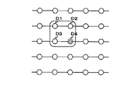
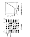
LED、CRT、LCD等の表示素子を縦横に配列することにより画面を構成する画像表示装置は、比較的小型のものから、屋外用の大型のものまで幅広く用いられている。図39に、LED等の表示素子を用いた画像表示装置の表示画面の構造を示す。図39に示すように、R(赤色)、G(緑色)、B(青色)の3原色を表す表示素子を格子状に配列することにより構成される画像表示装置を示す。R、G、Bの各表示素子は所定のパターンにより配列されている。図示するように、y=0のラインでは、図中左からB素子と、R素子とが交互に配列されており、y=1のラインでは、R素子と、G素子とが交互に配列されている。
【0003】
図39に示す表示画面に画像表示を行うには、まず入力画像を表す画像信号を所定のサンプリング周期でサンプリングすることによりR、G、Bの各階調値を表す画素データを各表示素子に対応して生成する。生成された画素データの各表示素子の発光色に対応する階調値に基づいて各表示素子を駆動する。ここで、図39に示す画像表示装置の表示画面は、G、B素子の2倍のR素子を備えているので、各R素子の表示レベル(発光レベル)は、画素データにより表されるR階調値の1/2とする。例えば、画面全体を白色とする場合、各表示素子に対応する画素データは(R,G,B)=(1,1,1)となる。ここで、R素子は図39に示すように、G、B素子の2倍配設されるので、R素子の表示レベルは画素データにより表されるR階調値の1/2とする。これにより、各表示素子の表示レベルはR=0.5、G=1、B=1となり、画面全体が白色として視認される。
【0004】
【発明が解決しようとする課題】
図39に示す画像表示装置の表示画面は、同じ色、あるいは類似した色の画像領域が、表示素子に比べて十分に大きいような画像、例えば周波数成分の低い自然画については本来の色を表示することができる。しかし、文字情報やグラフィック情報等の高周波成分を多く含む画像を表示する場合、以下に述べる偽色が発生する問題があった。
【0005】
図40は偽色の発生について説明するための説明図である。図40(a)は、PC等により出力される高周波成分を多く含む画像をサンプリングすることにより生成された画素データを模式的に示す図である。図40(a)に示す画素データによれば、黒色背景に1ドットの白線が表示される。同図において、黒色背景を表す画素データは(R,G,B)=(0,0,0)であり、白線を表す画素データは(R,G,B)=(1,1,1)である。図40(a)に示す画像データに基づいて図39に示す表示画面を有する画像表示装置を駆動した場合、各表示素子の表示レベルは図40(b)のようになる。つまり、図40(a)に示す白線に対応する領域には、R素子、およびG素子しか存在しないため、RとGとの混色により本来白色として表示されなければならない線が、RとGとの混色により黄色あるいは黄緑として視認される。
【0006】
図39に示すように、R、G、Bの各色を表す表示素子を縦横に配列して表示画面を構成する画像表示装置においては、図40(b)に示したように、高周波成分を多く含む画像を表示する際、本来の色と異なる色が表示される偽色が生じる。近年、パーソナルコンピュータ(以下、PCと称す)や、ワークステーション(WS)の発達に伴い、文字情報やグラフィック情報等の高周波成分を多く含む画像を表示する機会が増加している。こうした偽色の発生により、本来表現されるべき色が制限されるため、ユーザーが表示内容を正確に理解する上での妨げとなる。
【0007】
本発明は、上記のような問題点を解決するためになされたもので、複数の色を表す発光素子を縦横に配列することにより構成される表示手段に偽色を発生することなく画像を表示することが可能な画像表示装置をおよび画像表示方法を提供することを目的とする。
【0008】
【課題を解決するための手段】
本発明による画像表示装置は、複数の各色を表す複数の表示素子を2次元に配列して構成される表示手段に、R,G,Bの画像信号により表される入力画像に対応する画像を表示する画像表示装置であって、
前記R,G,Bの画像信号の各々を各表示素子に応じてサンプリングすることにより、R,G,Bの各色を表す単色画素データからなる画素データを、前記各表示素子に対応して生成する手段と、
前記画素データを構成する前記単色画素データの各々に平滑化処理を行うことにより平滑化された前記単色画素データからなる平滑化画素データを算出する手段と、
前記平滑化画素データを構成する前記単色画素データのいずれかを、前記表示素子の各表示色に応じて選択することにより、前記表示素子の表示レベルを示す表示データを出力する手段と、
前記表示データに基づいて前記各表示素子を駆動する手段とを備えたものである。
【0019】
本発明による画像表示方法は、複数の各色を表す複数の表示素子を2次元に配列して構成される表示手段に、R,G,Bの画像信号により表される入力画像に対応する画像を表示する画像表示方法であって、
前記R,G,Bの画像信号の各々を各表示素子に応じてサンプリングすることにより、R,G,Bの各色を表す単色画素データからなる画素データを、前記各表示素子に対応して生成し、
前記画素データを構成する前記単色画素データの各々に平滑化処理を行うことにより平滑化された前記単色画素データからなる平滑化画素データを算出し、
前記平滑化画素データを構成する前記単色画素データのいずれかを前記表示素子の各表示色に応じて選択することにより、前記表示素子の表示レベルを示す表示データを出力し、
前記表示データに基づいて前記各表示素子を駆動することにより前記画像の表示を行うものである。
【0030】
【発明の実施の形態】
実施の形態1.
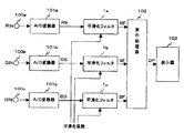
図1は本実施の形態による画像表示装置の構成を示す図であり、図2は表示器103の構成を示す図である。入力画像を表すR、G、B信号RIN、GIN、BINは、端子100a、100b、100cを介してA/D変換器101a、101b、101cにそれぞれ入力される。A/D変換器101a、101b、101cは、R、G、B信号RIN、GIN、BINを所定のサンプリング周期でサンプリングし、表示器103の各表示素子に対応する画素データRS、GS、BSを生成して出力する。RS、GS、BSはそれぞれ、一画素を表すR、G、Bの各階調を表す単色画素データである(ここでは、画素データを構成するRS、GS、BSのそれぞれを単色画素データと称する)。表示器103は、R、G、Bを表すLED等の表示素子を縦横の2次元に配列することにより構成される。A/D変換器101a、101b、101cは、図2に示す表示器103の各表示素子に対応して画素データRS、GS、BSを生成し、平滑化フィルタ1a、1b、1cに出力する。つまり、表示素子を垂直方向200ドット、水平方向300ドット配列して表示器103を構成した場合は、これと同数の200×300ドット分の画素データが生成される。
【0031】
平滑化フィルタ1a、1b、1cは、画素データRS、GS、BSに基づいて入力画像の平滑化を行い、平滑化された画像を表す平滑化画素データRF、GF、BFを算出し、表示処理器102に出力する。表示処理器102は、表示器103の表示素子の配列構成に基づいて、平滑化画素データRF、GF、BFから表示素子の発光色に対応する単色画素データを選択し、各表示素子の表示レベル(発光レベル)を示す表示データDPを出力する。例えば図2において、一点鎖線によりした位置にはB素子が配置されているので、対応する画素データの単色データBFに基づいてB素子の表示レベルが設定され、この発光レベルを示す表示データDPが表示器103に出力される。表示器103は、表示データDPに基づいて各表示素子を駆動することにより画像を表示する。
【0032】
図3は、平滑化フィルタ1a、1b、1cの構成を示す図である。同図においては、画素データRS、GS、BSを総称して画素データDとして示す。画素データ抽出手段90は平滑化演算の対象となる画素データD4とともに平滑化演算に用いる画素データD1、D2、D3を参照データとして抽出する。具体的には、図4(a)に示すように、2×2ドットの領域を表す画素データを抽出する。図3に示す画素データ抽出手段90において、1H遅延器2は、入力に対して1水平期間の遅延を与える遅延回路であり、DFF3a、3bはサンプリング周期の1周期分の遅延を与える遅延回路である。DFF3aは画素データD4の1サンプリング周期前の画素データD3を出力する。1H遅延器2は、画素データD4の1水平期間前の画素データD2を出力し、DFF3bは画素データD3の1水平期間前の画素データD1を出力する。
【0033】
加重平均演算器4は、平滑化係数K1、K2、K3、K4を重み係数とし、画素データD1、D2、D3、D4を用いた重み付き平均演算を行うことにより、画素データD4の平滑化画素データDFを出力する。乗算器5c、5d、5a、5bは、画素データD1、D2、D3、D4に平滑化係数K1、K2、K3、K4を乗じる。図4(a)および図4(b)は、各画素データD1〜D4と、これに乗じる平滑化係数K1〜K4との対応関係を示している。乗算結果K3・D3、K4・D4、K1・D1およびK2・D2は加算器6により加算され、加算結果K1・D1+K2・D2+K3・D3+K4・D4は、画素データD4に対応する平滑化画素データDFとして出力される。ここで、図3に示す平滑化画素データDFは、図1に示す平滑化フィルタ1a、1b、1cにより出力される平滑化画素データRF、GF、BFに対応している。
【0034】
図5に平滑化係数K1〜K4の設定値の具体例を示す。図5(a)に示すように、K1=K2=K3=K4=0.25とした場合、平滑化画素データDFは画素データD1〜D4の相加平均の値となる。図5(c)に示すように、K4=1、K1=K2=K3=0とした場合、DF=D4となり、入力された画素データD4がそのまま出力されることにより平滑化は行われない。図5(b)に示すように、K2=K3=0.2,K1=0.1,K4=0.5とした場合、平滑化量、すなわち平滑化の程度は、図5(a)、および図5(c)に示す平滑化係数の中間となる。このように、所望のK1〜K4を設定することにより、平滑化量を所望の量とすることができる。
【0035】
図6は図40(a)に示す画像を入力画像として、図5(a)に示す平滑化係数(K1=K2=K3=K4=0.25)を用いて平滑化処理を行なった場合の表示画像を示す図である。図40(a)に示す幅1ドット、表示レベル1の白色の縦線(x=3)は、平滑化処理により、幅2ドット、表示レベル0.5の縦線(x=3,4)となる。従って、x=3,4に配された各表示素子の平滑化画素データ(RF,GF,BF)は、(0.5,0.5,0.5)となる。これにより、x=3,4に配置されたR、G、Bの表示素子が点灯される。ここで、G、B素子の表示レベルは0.5となる。R素子は、G、B素子の2倍配設されているので、R素子の表示レベルは平滑化画素データRFに1/2を乗じた0.25となる。図6の領域Aにおける、R、G、B素子の表示レベルの総和はいずれも0.5となるので領域Aは白色として視認される。つまり、表示画像は2ドット幅の(x=3,4)白色の縦線として視認されるので、偽色の発生を防ぐことができる。
【0036】
尚、図3に示す平滑化フィルタ1は、2×2ドットの4つの画素データに基づいて平滑化演算を行なっているが、さらに多くの画素データに基づいて平滑化演算を行なってもよい。図7は、3×3ドットの領域を表す9ドットの画素データに基づいて平滑化演算を行う場合の画素データD1〜D9、および平滑化係数K1〜K9との対応関係を示す図である。図7(a)において、D5は平滑化の対象となる画素データを示している。図7(b)に示す対応関係に基づいて、平滑化係数K1〜K9を乗じた各画素データD1〜D9を加算した重み付き平均値K1・D1+K2・D2+K3・D3+K4・D4+K5・D5+K6・D6+K7・D7+K8・D8+K9・D9が、画素データD5の平滑化画素データとして出力される。
【0037】
図8に平滑化係数K1〜K9の設定値の具体例を示す。図8(a)に示すように、画素データD5の平滑化係数をK5=0.12、その他の平滑化係数を0.11とした場合に得られる平滑化画素データは、D1〜D9の相加平均値に近いデータとなる。図8(c)に示すように、画素データD5の平滑化係数をK5=1、他の平滑化係数を0とした場合に得られる平滑化画素データはD5となり、画素データD5がそのまま出力されることにより、平滑化は行われない。図8(b)に示すように、画素データD5の平滑化係数をK5=0.6とし、他の平滑化係数を0.05とした場合、平滑化量は図8(a)、および図8(c)に示す平滑化係数を用いた場合の中間となる。尚、4ドット×4ドット以上の画像データについて平滑化を行ってもよい。
【0038】
上記説明では水平方向および垂直方向に配列する画素データに基づいて平滑化演算を行なう2次元の平滑化フィルタを用いる構成としたが、水平方向あるいは垂直方向に配列する画素データに基づいて平滑化演算を行う1次元の平滑化フィルタを用いてもよい。例えば、図4に示す画素データD4の平滑化画素データを水平方向の1次元の平滑化フィルタを用いて算出するには、画素データD3、D4に基づいて加重平均演算を行う。この場合、水平方向の高周波成分に生じる偽色を抑制することができる。また、図4に示す画素データD4の平滑化画素データを垂直方向の1次元平滑化フィルタを用いて算出するには、画素データD2、D4に基づいて加重平均演算を行う。この場合、垂直方向の高周波成分に生じる偽色を抑制することができる。これらの水平方向、および垂直方向の1次元平滑化フィルタによる平滑化演算を順次行なうことにより、2次元の平滑化フィルタと同等の平滑化演算を行なってもよい。
【0039】
図5、8に示す平滑化係数は、表示画像と入力画像の明るさが等しくなるよう各平滑化係数の総和が1となるように設定されている。これに対し、平滑化係数の総和が1よりも大きくなるように各平滑化係数の値を設定した場合は、表示画像のコントラストは向上する。反対に、平滑化係数の総和が1よりも小さくなるように各平滑化係数の値を設定した場合、表示画像のコントラストは低下する。従って、平滑化係数の総和を1に対して変化するように各平滑化係数の値を設定することによりコントラストの調整を行なうことができる。
また、平滑化係数の総和をR、G、Bの各単色画素データ毎に異なるように設定することにより白バランスを調整することができる。
【0040】
実施の形態2.
実施の形態1において述べたように、入力画像の平滑化を行なうことにより、高周波成分を多く含む画像の偽色の発生を防ぐことができる。しかし、高周波成分の少ない画像領域に対して、平滑化処理を行なった場合、画像の鮮鋭度が劣化する。本実施の形態による画像表示装置は、入力画像の高周波成分を検出し、その検出結果に基づいて平滑化処理に用いる平滑化係数を制御することにより、不要な平滑化処理により生じる鮮鋭度の劣化を防ぐものである。
【0041】
図9は本実施の形態による画像表示装置の構成を示す図である。高周波検出器7a、7b、7cは、画素データRS、GS、BSの高周波成分を検出し、その検出量を表す高周波検出値RH、GH、BHを平滑化係数発生器8a、8b、8cに出力する。平滑化係数発生器8a、8b、8cは、高周波検出値RH、GH、BHに基づいて平滑化係数KR、KG、KBを発生し、平滑化フィルタ1a、1b、1cに出力する。
【0042】
図10は高周波検出器7a、7b、7cの構成を示す図である。同図においては、各単色画素データRS、GS、BSを相称して画素データDにより示し、高周波検出値RH、GH、BHを総称してDHにより示す。画素データ抽出手段91は、高周波検出値DHの算出に用いる画素データD1〜D4を参照データとして抽出する(画素データ抽出手段91の構成、および動作については実施の形態1において説明した画素データ抽出手段90と同様である)。画素データD1〜D4は図11に示す2×2ドットの領域を表す4つの画像データに対応している。画素データD4の高周波検出値DHは、画素データD1〜D4に基づいて算出される。
【0043】
図12は図10に示した高周波成分算出器11の構成を示す図である。減算器12a、12b、12cは、画素データD4と、画素データD1、D2、D3との減算を行ない、減算結果D4−D1、D4−D2、D4−D3を絶対値算出器13a、13b、13cにそれぞれ出力する。絶対値算出器13a、13b、13cは入力された各減算結果の絶対値|D4−D1|、|D4−D2|、|D4−D3|を最大値算出器14に出力する。最大値算出器14は、絶対値|D4−D1|,|D4−D2|、|D4−D3|から最大値を選択し、高周波検出値DHとして出力する。高周波検出値DHは、画素データD4と、画素データD1、D2、D3との差分絶対値の最大値であり、高周波成分が大きいほど高周波検出値DHの値は大きくなる。図12において、高周波検出値DHは、図9に示す高周波検出器7a、7b、7cから出力される高周波検出値RH、GH、BHに対応する。各高周波検出器7a、7b、7cから出力される高周波検出値RH、GH、BHは、平滑化係数発生器8a、8b、8cに入力される。
【0044】
図13は平滑化係数発生器8a、8b、8cの構成を示す図である。LUT15はルックアップテーブルである。図13では、高周波検出器7a、7b、7cからそれぞれ出力される高周波検出値RH、GH、BHを総称してDHとし、各平滑化フィルタ1a、1b、1cに出力される平滑化係数KR、KG、KBを総称してKDとして表す。LUT15は入力された高周波検出値DHに基づいて、LUT15から所定の平滑化係数KD(KD1〜KD4)を読み出して出力する。
【0045】
LUT15には、高周波検出値DHに対応する平滑化係数KD1〜KD4がLUTデータとして格納される。LUTデータは、外部から与えられる平滑化係数制御信号を介してLUT15に書き込まれる。図14はLUT15に格納されるLUTデータの一例を示す図である。同図に示すように、高周波検出値DHが0/255から255/255の値をとるものとして、各高周波検出値DHの値に対応する平滑化係数KD1〜KD4が格納されている。例えば、DH=0/255に対してはKD1=KD1(0)、KD2=KD2(0)、KD3=KD3(0)、KD4=KD4(0)がLUT15のアドレス0番地に格納されている。つまり、高周波検出値DHに対応するアドレス入力をLUT15に与えることにより、予め定められた平滑化係数KD1〜KD4をLUT15から読み出すことができる。
【0046】
図15はLUT15の入出力特性の一例を示す図であり、高周波検出値DHに対応する平滑化係数KDの値を示している。図15(a)は画素データD4の平滑化係数KD4の特性を示しており、図15(b)は画素データD1〜D3の平滑化係数KD1〜KD3の特性を示している。図15に示すように、高周波検出値DHがSH1により示す所定の閾値よりも低い場合(領域L)、平滑化係数はKD1=KD2=KD3=0、KD4=1となり、入力された画素データD4がそのまま出力される。つまり、図5(c)に示す平滑化係数が出力され、平滑化は行われない。一方、高周波検出値DHがSH2により示す所定の閾値以上の場合(領域H)、出力される平滑化係数はK1=K2=K3=K4=0.25となり、相加平均演算が行われる。つまり、図5(a)に示す平滑化係数により平滑化演算が行なわれる。平滑化係数DHがSH1≦DH<SH2の場合(領域M)、平滑化係数は0.25<K4<1、K1=K2=K3=(1−K4)/3となる。この場合、例えば図5(b)に示す平滑化係数が出力される。
【0047】
図15に示す特性に基づいて平滑化係数KD(KD1〜KD4)を設定し、LUT15に格納することにより、高周波成分が少ない領域Lにおいては平滑化が行われず、高周波成分が多い領域Hにおいては平滑化量の多い平滑化係数が出力される。また、領域Mにおいては高周波成分の量に対応して平滑化量が連続的に変化する。これにより、画像の鮮鋭度を劣化させることなく高周波画像領域に生じる偽色の発生を抑制することができる。
【0048】
実施の形態3.
実施の形態2では、平滑化係数発生器8a、8b、8c(図9参照)をLUT15(図13参照)により構成したが、ルックアップテーブルを用いた場合、回路規模が大きくなる。本実施の形態では、平滑化係数を演算により生成することが可能な平滑化係数発生器について示す。
【0049】
図16は、本実施の形態による平滑化係数発生器8a、8b、8cの構成を示す図である。図17は、図16に示す平滑化係数発生器の入出力特性を示す図であり、高周波検出値DHに対する平滑化係数KDの値を示している。図17(a)においてα1、α2は平滑化係数KD4に関するパラメータであり、図17(b)においてβ1、β2は平滑化係数KD1、K2、KD4に関するパラメータである。SH1、SH2は高周波検出値DHに関する閾値である。各制御パラメータ、および閾値は平滑化係数制御信号(図9参照)を介して外部から与えられる。本実施の形態において、各パラメータはα1=1、α2=0.25、β1=0、β2=0.25とする。
【0050】
図17に示すように、高周波検出値DHがDH<SH1である領域Lにおいて、平滑化係数はKD1=KD2=KD3=β1(=0)、KD4=α1(=1)となり、図5(c)に示す平滑化係数が出力される。高周波検出値DHがSH2≦DHである領域Hにおいて、平滑化係数はK1=K2=K3=β2(=0.25)、K4=α2(=0.25)となり、図5(a)に示す平滑化係数が出力される。高周波検出値DHがSH1≦DH<SH2である領域Mにおいて、平滑化係数はKD1=KD2=KD3=Fβ(DH)、K4=Fα(DH)により与えられ、例えば図5(b)に示す平滑化係数が出力される。ここでFα(DH)、およびFβ(DH)は以下の式(1)(2)により与えられる。
【0051】
【数1】

以下、図16に基づいて本実施の形態による平滑化係数発生器8a、8b、8cの動作を説明する。
比較器23は、高周波検出値DHと、閾値SH1、および閾値SH2との大小関係を比較することにより、高周波検出値DHが図17に示す領域L、領域M、領域Hのいずれに属するかを判別し、判別結果を選択器33、34に出力する(つまり、DH<SH1の場合は領域L、SH1≦DH<SH2の場合は領域M、SH2≦DHの場合は領域Lの判別結果を出力する)。
【0053】
減算器24は、DHからSH1を減算した減算結果を除算器28に出力する。減算器25はSH2からSH1を減算し、減算結果を除算器28に出力する。減算器26はα2からα1を減算し、減算結果を乗算器29に出力する。減算器27はβ2からβ1を減算し、減算結果を乗算器30に出力する。除算器28は、減算器24の出力を減算器25の出力で割った除算結果(DH−SH1)/(SH2−SH1)を乗算器29および30に出力する。
【0054】
乗算器29は、減算器26の出力に除算器28の出力を乗じた乗算結果(DH−SH1)・(α2−α1)/(SH2−SH1)を加算器31に出力する。加算器31は乗算器29の出力とパラメータα1との加算結果であるFα(DH)(式1参照)を選択器33に出力する。乗算器30は、減算器27の出力に除算器28の出力を乗じた乗算結果(DH−SH1)・(β2−β1)/(SH2−SH1)を加算器32に出力する。加算器32は乗算器30の出力とパラメータβ1との加算結果であるFβ(DH)(式2参照)を選択器34に出力する。
【0055】
選択器33は、比較器23の比較結果に基づいて、パラメータα1、α2、および加算器31から出力されるFα(DH)のいずれかを選択し、平滑化係数KD4として出力する。つまり、比較器23の比較結果が領域Lを示す場合はKD4=α1、領域Mを示す場合はKD4=Fα(DH)、領域Hを示す場合はKD4=α2を出力する。同様に、選択器34は、比較器23の比較結果に基づいて、パラメータβ1、β2、加算器32から出力されるFβ=(DH)のいずれかを選択し、平滑化係数KD1〜KD3として出力する。つまり、比較器23の比較結果が領域Lを示す場合はKD1〜KD3=β1、領域Mを示す場合はKD1〜KD3=Fβ(DH)、領域Hを示す場合はKD1〜KD3=β2を出力する。
【0056】
図17に示すように、領域Mの平滑化係数を、高周波検出値DHに基づいて連続的に変化させることにより、ノイズなどの影響により高周波検出値DHが変動するような場合でも、平滑化係数が段階的に変化する。このため、ノイズなどの影響による平滑化特性の急激な変化を防ぐことができる。
【0057】
図18は本実施の形態による平滑化係数発生器8a、8b、8cの他の構成を示す図である。図19は、図18に示す平滑化係数発生器8a、8b、8cの入出力特性を示す図である。図19に示すように、高周波検出値DHがDH<SH1である領域Lにおいて、平滑化係数はKD1=KD2=KD3=β1(=0)、KD4=α1(=1)となり、図5(c)に示す平滑化係数が出力される。高周波検出値DHがDH≧SH1である領域Hにおいて、平滑化係数はKD1=KD2=KD3=β2(=0.25)、KD4=α2(=0.25)となり、図5(a)に示す平滑化係数が出力される。
【0058】
以下、図18に示す平滑化係数発生器の動作について説明する。比較器21は、高周波検出値DHと外部から設定される閾値SH1とを比較し、高周波検出値DHが領域L、または領域Hのいずれに属するかを判別し、判別結果を選択器22に出力する。選択器22には、平滑化係数制御信号に基づいてパラメータα1、α2、β1、β2が与えられる。ここで、各パラメータはα1=1、α2=0.25、β1=0、β2=0.25である。選択器22は、比較結果がDH<SH1(領域L)の場合、平滑化係数KD4としてα1=1を選択し、平滑化係数KD1〜KD3としてβ1=0を選択して出力する。一方、比較結果がDH≧SH1(領域H)の場合は、平滑化係数KD4としてα2=0.25を選択し、平滑化係数KD1〜KD3としてβ2=0.25を選択して出力する。
【0059】
実施の形態4.
実施の形態2に示す高周波成分算出器11(図12参照)は、画素データD4と画素データD1、D2、D3との差分値の絶対値|D4−D1|、|D4−D2|、|D4−D3|の最大値を高周波検出値DHとして出力するため、ノイズの多い画像データが入力された場合、ノイズ成分を高周波検出値DHとして検出する可能性がある。本実施の形態は、ノイズによる誤検出を抑制することが可能な高周波検出器に関する。
【0060】
図20に示す高周波成分算出器11は、平均値算出器16により、絶対値算出器13a、13b、13cから出力される絶対値|D4−D1|,|D4−D2|、|D4−D3|の平均値を高周波検出値DHとして出力する。このように、画素データD4と画素データD1、D2、D3との差分値の平均値を高周波検出値DHとすることにより、ノイズの多い画像データであってもノイズ成分が平均化されるので、高周波検出の誤動作を抑制することができる。
【0061】
図21に示す他の高周波成分算出器11は、メディアンフィルタ17により、絶対値|D4−D1|,|D4−D2|、|D4−D3|の3つの絶対値から中間の値を選択し,その結果を高周波検出値DHとして出力する。
上記のように算出される高周波検出値DHは、画素データD4とその他の画素データD1〜D3との差分値の中間値である。そのため、ノイズの多い画像データであっても,ノイズ成分による極端に大きいあるいは小さい値は選択されないので、高周波検出の誤動作を抑制することができる。
【0062】
図22に示す高周波成分算出器11は、画素データD4と、画素データD1、D2、D3の平均値との差分絶対値を高周波検出値DHとして出力するものである。つまり、平均値算出器18は画素データD1、D2、D3の相加平均(D1+D2+D3)/3を出力する。減算器19は、単色データD4と平均値(D1+D2+D3)/3との減算を行い、減算結果D4−(D1+D2+D3)/3を出力する。絶対値算出器20は、入力された減算結果の絶対値|D4−(D1+D2+D3)/3|を算出して高周波検出値DHとして出力する。
上記のように算出される高周波検出値DHは、演算対象となる画素データD4とその他のD1、D2、D3の平均値との差分絶対値である。そのため、ノイズの多い画像データであっても画素データD1、D2、D3におけるノイズ成分が平均化されるので、誤検出を抑制することができる。
【0063】
以上においては、2×2ドットの範囲において高周波成分の検出を行う構成について説明したが、3×3ドットの範囲において高周波成分の検出を行う構成としてもよい。この場合、検出する周波数成分をより自由に与えることができる。例えば、n、mを正の整数として、n×mドットの範囲において高周波成分の検出を行う構成としてもよく,これも同様の効果を奏する。
【0064】
実施の形態5.
実施の形態2に示す画像表示装置では、平滑化フィルタ1a、1b、1c(図3参照)、および高周波検出器7a、7b、7c(図10参照)は、画素データ抽出手段90、91により画素データD1〜D4を抽出し、演算を行っているが、図23に示すように、平滑化フィルタ51a、51b、51cにより抽出される画素データD1〜D4を参照データRref、Gref、Bref(これらを総称してDrefとする)として高周波検出器57a、57b、57cに出力するように構成してもよい。つまり、図24に示すように、平滑化フィルタ51a、51b、51cにより抽出される画素データD1〜D4を参照データDrefとして外部に出力するよう構成し、この参照データDrefを図25に示す高周波検出器57a、57b、57cの高域成分算出器11に入力するよう構成する。これにより、高周波検出器57a、57b、57cの画素データ抽出手段を省略し、回路規模を縮小することができる。
【0065】
実施の形態6.
実施の形態1、2に示す画像表示装置(図1、9参照)は、アナログ画像信号を入力の対象としていたが、デジタル画像信号を直接入力するように構成してもよい。
【0066】
図26は、本実施の形態による画像表示装置の構成を示す図である。デジタル画像信号を構成する画素データRD、GD、BDは、端子35a、35b、35cを介して平滑化フィルタ1a,1bおよび1cに入力される。ここで、デジタル画像信号は、デジタルテレビ放送の受信データであってもよいし、デジタルインタフェース手段の出力であってもよい。また、アナログ画像信号をA/D変換した出力であってもよい。平滑化フィルタ1a、1b、1cは、画素データRD、GD、BDを平滑化し、平滑化画素データRF、GF、BFを表示処理器102に出力する。表示処理器102は、平滑化画素データRF、GF、BFに基づいて表示器103の各表示素子を駆動し、画像が表示される。
【0067】
実施の形態7.
実施の形態1において述べたように、図2に示す画像表示装置の表示器103は、LEDにより構成することができる。LEDは線形的な電気−光変換特性となるよう駆動されるため、ガンマ補正処理等が行われた画像信号が入力される場合は、逆ガンマ変換等の階調変換処理を行なう必要がある。また、ユーザーの好みや周囲環境(屋外、室内など)に応じて階調変換処理を行う場合もある。本実施の形態は、階調変換処理手段を備えた画像表示装置に関する。
【0068】
図27は、本実施の形態による画像表示装置の構成を示す図である。非線形階調変換器36a、36b、36cは、A/D変換器101a、101b、101cから出力される画素データRS、GS、BSに対して階調変換を行い、変換後の画素データRT、GT、BTを平滑化フィルタ1a、1b、1cにそれぞれ出力する。図28は非線形階調変換器36a、36b、36cの構成を示す図である。LUT150は、階調変換特性を表すLUTデータに基づいて画素データRS、GS、BSの階調特性を変換し、変換された画素データRT、GT、BTを出力する(図28においては、画素データRS、GS、BSを総称してDとし、階調特性変換後の画素データをRT、GT、BTを総称してDTにより示している)。図29はLUT150に格納された階調変換特性の一例を示す図である。横軸はLUT150に入力される画素データDを示し、縦軸は出力される画素データDTを示す。図29に示す階調変換特性は、DT=Dγ(γ=1,1.5,2,2.2,3,4)により表される。
【0069】
図27に示すように、非線形階調変換器36a、36b、36cは、階調変換に起因する偽色の発生を防止するため、平滑化フィルタ1a、1b、1cの前段に設けられている。以下、非線形階調変換器36a、36b、36cを平滑化フィルタ1a、1b、1cの後段に設けた場合に生じる偽色の問題について説明する。
【0070】
図30(a)はグレーを表す画像の一例を示す図である。同図に示すグレーの画像は、2ドット×2ドットの白データ(図中○により表す)、および黒データ(図中●により表す)を市松模様状に配列して構成される。白データはRS=GS=BS=1、黒データはRS=GS=BS=0である。図30(b)は非線形階調変換器36a、36b、36cの階調変換特性の一例(DT=D2の場合)を示す図である。図31は、図30に示す入力画像を平滑化フィルタ1a、1b、1cにより平滑化した後に、階調変換を行なう場合、つまり非線形階調特性変換器36a、36b、36cを平滑化フィルタ1a、1b、1cの後段に設けた場合の問題点について説明するための説明図である。図31は、図30(a)に示す入力画像の領域Sに対応する画像データのA/D変換器101a、101b、101cの出力RS(図31(1))、平滑化フィルタ1aの出力RF(図31(2))、非線形階調変換器36a、36b、36cの出力RT(図31(3))、および表示処理器102の出力DP(図31(4))の例を示している。
【0071】
図31(4)に示すように、階調変換を平滑化処理の後に行なった場合、R素子の表示レベルの総和は0.125×8=1、G素子の表示レベルの総和は1×2+0×2=2、B素子の表示レベルの総和は0.25×4=1となる。つまり、R、G、B素子の各表示レベルの比は1:2:1となり、無彩色として表示されるべき画像が緑がかった表示画像となってしまう。このように、非線形階調変換器36a、36b、36cを平滑化フィルタ1a、1b、1cの後段に備えた場合、表示画像に偽色が発生する。
【0072】
図32は非線形階調変換器36a、36b、36cを平滑化フィルタ1a、1b、1cの前段に設けた場合のA/D変換器101の出力RS(図32(1))、非線形階調変換器36の出力RT(図32(2))、平滑化フィルタ1a、1b、1c(図32(3))の出力RF、および表示処理器102の出力DP(図32(4))を示している。非線形階調変換器36a、36b、36cを平滑化フィルタ1a、1b、1cの前段に設けた場合、図32(4)に示すように、R素子の表示レベルの総和は0.25×8=2、G素子の表示レベルの総和は0.5×4=2、B素子の表示レベルの総和は0.5×4=2となる。つまり、R、G、B素子の各表示レベルの総和は全て2となり、表示画像は灰色のような無彩色として視認される。このように非線形階調変換器36を平滑化フィルタ1よりも前段に備える場合、偽色は発生しない。
【0073】
以上のように、平滑化処理と階調変換処理の順序は重要であり、画像信号の階調特性の変換を行う場合、図27に示すように、非線形階調変換器36は、平滑化フィルタ1の前段に設けなければならない。上記の構成により、表示画像の偽色の発生を抑制するとともに、階調特性の補正を行うことができる。
尚、非線形階調変換器36は、LUT(ルック・アップ・テーブル)を用いたが、演算によって変換データを算出する構成としてもよい。
【0074】
実施の形態8.
図2に示す表示器103の表示素子としてCRTやLCDといった非線形な電気−光変換特性を有する素子を用いる場合、ガンマ補正等により表示素子の非線形性を補正する必要がある。図33は、本実施の形態による画像表示装置の構成を示す図である。逆特性階調変換器37は、表示処理器102により出力される表示データDPの階調特性を変換することにより、表示器104の電気−光変換特性を補正する。図34は、表示器104の階調特性の例を示す図である。図34(a)はCRT、図34(b)はLCDの階調特性を示しており、いずれも非線形な特性を有する。図35(a)(b)はそれぞれ、CRT、LCDに対応した逆特性階調変換器37の変換特性を示す図である。図35(a)(b)に示すように、逆特性階調変換器37の階調特性は、表示器104の階調特性の逆関数として表される。従って、逆特性階調変換器37の出力データDNは、逆特性階調変換器37の階調特性をfnとするとDN=fn(DP)により表される。つまり、表示器104の表示素子の表示レベルは、表示器104の階調特性をfとするとf(DN)=f(fn(DP))となる。
【0075】
逆特性階調変換器37から出力される表示データDNは表示器104に出力され、表示器104は表示データDNに基づいて各表示素子を駆動する。
【0076】
上記のように、表示器104の表示素子としてCRT、やLCD等の非線形な電気−光変換特性を有する素子を用いる場合、これを補正する逆特性階調変換器37を設けることにより入力画像に忠実な画像を表示することができる。
【0077】
実施の形態9.
実施の形態2に示す画像表示装置(図9参照)は、画素データRS、GS、BSに基づいて高周波検出値RH、GH、BHを検出しているが、画像データの輝度データに基づいて高周波検出を行なってもよい。図36は、本実施の形態による画像表示装置の構成を示す図である。輝度算出器39は、画素データRS、GS、BSに基づいて輝度データYを算出し、高周波検出器7に出力する。輝度データYは、例えば、以下の式により算出される。
【0078】
【数2】
![]()
高周波検出器7は、輝度データYに基づいて画像レベルの変化を検出し、高周波検出値YHを平滑化係数発生器8に出力する。平滑化係数発生器8は、高周波検出結果YHに基づいて平滑化係数KDを発生し、平滑化フィルタ1a、1b、1cに出力する。平滑化フィルタ1a、1b、1cは、平滑化係数発生器8により出力された平滑化係数KDに基づいて平滑化処理を行ない、平滑化画素データRF、GF、BFを算出し、表示処理器102に出力する。
【0080】
実施の形態2では図9に示すように、高周波検出器1a、1b、1c、および平滑化係数発生器8a、8b、8cを各3つ備えている。これに対し、輝度データYにより高周波検出を行う本構成によれば、高周波検出器1a、1b、1c、および平滑化係数発生器8a、8b、8cを単一化することができるので、回路規模を縮小することができる。
【0081】
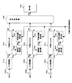
実施の形態10.
図37は、本実施の形態による画像表示装置の構成を示す図である。同図に示す画像表示装置はn種類の画像信号が入力されるR1〜Rn、G1〜Gn、B1〜Bnの複数の端子を備えている。各端子からは、NTSC、ハイビジョン等のテレビ画像信号や、PCから出力される画像信号といったフォーマットの異なる画像信号が入力される。各端子に入力される画像信号のフォーマットは予め設定されており、信号切替器40は外部から入力される切替信号SELに基づいて画像信号を選択する。信号切替器40は、選択した画像信号のR、G、B信号を、A/D変換器101a、101b、101cにそれぞれ出力する。A/D変換器101a、101b、101cは、R、G、Bの各画像信号を所定のサンプリング周期でサンプリングすることにより画素データRS、GS、BSを生成し、平滑化フィルタ1a、1b、1cに出力する。
【0082】
コントローラ41は、切替信号SELに基づいて、選択された画像信号のフォーマットを特定する。コントローラ41には切替信号SELに対応する画像信号のフォーマット情報が格納されている。コントローラ41は、特定された画像信号のフォーマットに基づいて、平滑化係数KDを発生し、各平滑化フィルタ1a、1b、1cに出力する。例えば、画素数が多い画像は高周波成分を多く含む場合が多いので、平滑化量の多い平滑化係数KDを出力する。反対に、画素数が少ない画像は高周波成分が少ない場合が多いので、偽色は発生しにくい。従って、平滑化量の少ない平滑化係数を出力することにより、平滑化処理により生じる鮮鋭度の劣化を防止する。
【0083】
上記の構成によれば、画像信号のフォーマットに応じて平滑化量を制御することにより、高周波成分の多い画像では偽色の発生を防止し、高周波成分の少ない画像では鮮鋭度の劣化を抑制するので、高画質の画像を表示することができる。尚、フォーマットに基づいて、表示画像の内容を判別し、平滑化係数を制御するよう構成してもよい。例えば、PCから出力される画像信号は、文字情報や、図形情報を多く含むので、高周波成分を多く含んでいる。これに対し、テレビ信号は自然画や、動画といった偽色の発生しにくい画像情報を含む。従って、選択された画像信号のフォーマットに基づいて、入力画像がPCの出力画像か、またはテレビ画像かを判別し、PC画像の場合は平滑化量を大きくすることにより偽色の発生を抑制し、テレビ画像の場合は平滑化量を小さくすることにより鮮鋭度の劣化を抑制するように構成してもよい。
【0084】
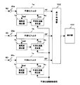
実施の形態11.
図38は、本実施の形態による画像表示装置の構成を示す図である。端子100a、100b、100cには任意のフォーマットの画像信号が入力される。A/D変換器101a、101b、101cは、入力された画像信号のフォーマットに従い、サンプリングを行い画素データRS、GS、BSを画像サイズ検出器42に出力する。
【0085】
画像サイズ検出器42は、画素データRS、GS、BS、および入力画像信号の同期信号に基づいて入力画像のサイズを検出し、検出された画像サイズをコントローラ41に出力する。コントローラ41にはまた、外部から表示器103の表示サイズ、つまり表示画面を構成する表示素子の数を示す表示サイズ情報が入力される。コントローラ41は、画像サイズ検出器42から出力される画像サイズ、および表示サイズ情報に基づいて変換倍率Zを発生する。変換倍率Zは、入力画像の画像サイズを表示画像サイズに変換するための変換倍率を表す。例えば、入力画像サイズが640×480ドット、表示サイズが1024×768ドットの場合、変換倍率Zは水平方向および垂直方向とも1.6倍となる。コントローラ41から出力された変換倍率Zは,画像サイズ変換器43に入力される。画像サイズ変換器43は、画素データRS、GS、BSに基づいて補間画素データを生成することにより画素数の変換を行い、画像のサイズを変換する。画像サイズ変換器43は、サイズ変換された画像の画素データRZ、GZ、BZを平滑化フィルタ1a、1b、1cにそれぞれ出力する。
【0086】
画像サイズの変換は、入力画像の画素データを補間する補間画素データを生成し、画素数を変換することにより行う。従って、拡大処理を行った場合、拡大画像においては輪郭部の鮮鋭度が低下する。これにより、拡大処理を行なった画像は入力画像に比べて高周波成分が減少し、偽色発生も少なくなる。特に、変換倍率が2倍以上の場合、拡大画像における輪郭部の鮮鋭度は大きく劣化する。このように、画像を拡大して表示する場合は、偽色の発生を抑制するよりも、画像の鮮鋭度の低下を抑制する必要がある。つまり、拡大画像の場合は、平滑化を行わないか、または平滑化量を少なくする必要がある。反対に、画像を縮小して表示する場合は、高周波成分が増加し、偽色の発生が生じる。従って、縮小率の大きい画像を表示する場合は、縮小率に応じて平滑化量を大きくする必要がある。コントローラ41は、変換倍率Zが大きい場合は平滑化量の少ない平滑化係数KDを出力し、反対に画像サイズの変換が行われない場合や、画像の縮小が行われる場合は、平滑化量の多い平滑化係数を出力する。
【0087】
コントローラ41は、変換倍率Zに基づいて発生した平滑化係数KDを、平滑化フィルタ1a、1b、1cに出力する。平滑化フィルタ1a、1b、1cは,画像サイズ変換された画素データRZ、GZ、BZに対して平滑化係数KDに基づく平滑化を行う。
【0088】
上記のように、入力画像のサイズを表示器103の表示画面を構成する表示素子の数に対応して変換して表示する際、変換倍率Zに応じて平滑化係数KDを制御し、平滑化量を調整する構成としたので、偽色の発生を抑制するとともに輪郭部における鮮鋭度の劣化を防ぐことにより高画質の画像を表示することができる。尚、デジタル画像データが入力された場合は、A/D変換を行わず、画像サイズ変換器43に直接出力されるよう構成してもよい。
【0089】
【発明の効果】
本発明による画像表示装置および画像表示方法は、各表示素子を一画素として入力画像を表す画素データを各表示素子に対応して生成し、平滑化された入力画像を表す画素データの平滑化画素データを算出し、各表示素子の表示レベルを平滑化画素データおよび各表示素子の各色に基づいて算出し、算出された表示レベルに基づいて各表示素子を駆動するので、偽色の発生を防ぐことができる。
【0090】
また、入力画像の高周波成分を検出し、その検出量に基づいて入力画像の平滑化量を制御するので、輪郭部における鮮鋭度の劣化を生じることなく偽色の発生を防ぐことができる。
【図面の簡単な説明】
【図1】 実施の形態1による画像表示装置の構成を示す図である。
【図2】 表示器の構成を示す図である。
【図3】 平滑化フィルタの構成を示す図である。
【図4】 平滑化フィルタの動作について説明するための説明図である。
【図5】 平滑化係数の一例を示す図である。
【図6】 実施の形態1による画像表示装置の表示画像の一例を示す図である。
【図7】 平滑化フィルタの動作について説明するための説明図である。
【図8】 平滑化係数の一例を示す図である。
【図9】 実施の形態2による画像表示装置の構成を示す図である。
【図10】 高周波検出器の構成を示す図である。
【図11】 高周波検出器の動作について説明するための説明図である。
【図12】 高周波成分算出器の構成を示す図である。
【図13】 平滑係数発生器の構成を示す図である。
【図14】 平滑係数発生器の構成を示す図である。
【図15】 平滑化係数の特性の一例を示す図である。
【図16】 平滑化係数発生器の他の構成を示す図である。
【図17】 平滑化係数の特性の一例を示す図である。
【図18】 平滑化係数発生器の他の構成を示す図である。
【図19】 平滑化係数の特性の一例を示す図である。
【図20】 高周波成分算出器の他の構成を示す図である。
【図21】 高周波成分算出器の他の構成を示す図である。
【図22】 高周波成分算出器の他の構成を示す図である。
【図23】 実施の形態5による画像表示装置の構成を示す図である。
【図24】 平滑化フィルタの構成を示す図である。
【図25】 高周波検出器の構成を示す図である。
【図26】 実施の形態6による画像表示装置の構成を示す図である。
【図27】 実施の形態7による画像表示装置の構成を示す図である。
【図28】 非線形階調変換器の構成を示す図である。
【図29】 非線形階調変換器の階調変換特性を示す図である。
【図30】 階調変換動作について説明するための説明図である。
【図31】 階調変換動作について説明するための説明図である。
【図32】 階調変換動作について説明するための説明図である。
【図33】 実施の形態8による画像表示装置の構成を示す図である。
【図34】 表示器の階調特性の一例を示す図である。
【図35】 逆特性階調変換器の階調変換特性の例を示す図である。
【図36】 実施の形態9によ画像表示装置の構成を示す図である。
【図37】 実施の形態10による画像表示装置の構成を示す図である。
【図38】 実施の形態11による画像表示装置の構成を示す図である。
【図39】 画像表示装置の構成を示す図である。
【図40】 従来の画像表示装置における問題について説明するための説明図である。
【符号の説明】
1a,1b,1c,51a,51b,51c 平滑化フィルタ、90,91 画素データ抽出手段、4 加重平均演算器、7a,7b,7c 高周波検出器、8,8a,8b,8c 平滑化係数発生器、11 高周波成分算出器,15,150 ルックアップテーブル、36a,36b,36c 非線形階調変換器、37 逆特性階調変換器、39 輝度算出器,40 信号切替器、41 コントローラ、42 画像サイズ検出器、43 画像サイズ変換器、101a,101b,101c A/D変換器、102 表示処理器、103,104 表示器。[0001]
BACKGROUND OF THE INVENTION
In the present invention, display elements such as light emitting diodes (LEDs), color cathode ray tubes (CRTs), and liquid crystal panels (LCDs) representing colors of R (red), G (green), and B (blue) are arranged vertically and horizontally. The present invention relates to an image display device that displays an image on a configured display screen, and an image display method.
[0002]
[Prior art]
2. Description of the Related Art Image display devices that form a screen by arranging display elements such as LEDs, CRTs, and LCDs vertically and horizontally are widely used from relatively small to large outdoor devices. FIG. 39 shows a structure of a display screen of an image display device using a display element such as an LED. As shown in FIG. 39, an image display device configured by arranging display elements representing three primary colors of R (red), G (green), and B (blue) in a grid pattern is shown. The R, G, and B display elements are arranged in a predetermined pattern. As shown in the figure, in the line y = 0, the B element and the R element are alternately arranged from the left in the figure, and in the line y = 1, the R element and the G element are alternately arranged. ing.
[0003]
In order to display an image on the display screen shown in FIG. 39, first, an image signal representing an input image is sampled at a predetermined sampling period, and pixel data representing R, G, and B gradation values are associated with each display element. And generate. Each display element is driven based on the gradation value corresponding to the emission color of each display element of the generated pixel data. Here, since the display screen of the image display device shown in FIG. 39 includes R elements twice as large as the G and B elements, the display level (light emission level) of each R element is represented by R. It is set to 1/2 of the gradation value. For example, when the entire screen is white, pixel data corresponding to each display element is (R, G, B) = (1, 1, 1). Here, as shown in FIG. 39, the R element is arranged twice as large as the G and B elements, so that the display level of the R element is ½ of the R gradation value represented by the pixel data. As a result, the display level of each display element is R = 0.5, G = 1, and B = 1, and the entire screen is visually recognized as white.
[0004]
[Problems to be solved by the invention]
The display screen of the image display device shown in FIG. 39 displays the original color for an image in which the image area of the same color or a similar color is sufficiently larger than the display element, for example, a natural image with a low frequency component. can do. However, when displaying an image containing a lot of high-frequency components such as character information and graphic information, there is a problem that false colors described below occur.
[0005]
FIG. 40 is an explanatory diagram for explaining the occurrence of false colors. FIG. 40A is a diagram schematically illustrating pixel data generated by sampling an image including a lot of high-frequency components output from a PC or the like. According to the pixel data shown in FIG. 40A, a one-dot white line is displayed on a black background. In the figure, pixel data representing a black background is (R, G, B) = (0, 0, 0), and pixel data representing a white line is (R, G, B) = (1, 1, 1). It is. When the image display apparatus having the display screen shown in FIG. 39 is driven based on the image data shown in FIG. 40A, the display level of each display element is as shown in FIG. That is, since only the R element and the G element exist in the region corresponding to the white line shown in FIG. 40A, the line that should be displayed as white originally by the color mixture of R and G is R and G. Is visually recognized as yellow or yellowish green.
[0006]
As shown in FIG. 39, in an image display device that configures a display screen by arranging display elements representing R, G, and B colors vertically and horizontally, as shown in FIG. When displaying an image including a false color, a color different from the original color is displayed. In recent years, with the development of personal computers (hereinafter referred to as PCs) and workstations (WS), there are increasing opportunities to display images containing a large amount of high-frequency components such as character information and graphic information. The occurrence of such false colors restricts the colors that should be originally expressed, which hinders the user from accurately understanding the display contents.
[0007]
The present invention has been made to solve the above-described problems, and displays an image without generating false colors on a display means configured by arranging light emitting elements representing a plurality of colors vertically and horizontally. An object of the present invention is to provide an image display device and an image display method that can be used.
[0008]
[Means for Solving the Problems]
An image display device according to the present invention displays an image corresponding to an input image represented by R, G, B image signals on display means configured by two-dimensionally arranging a plurality of display elements representing a plurality of colors. An image display device for displaying,
Said R, G, B Image By sampling each of the signals according to each display element , Means for generating pixel data composed of single-color pixel data representing each color of R, G, B corresponding to each display element;
The pixel data Each of the monochrome pixel data constituting By performing smoothing process A flat image comprising the smoothed monochrome pixel data. Means for calculating smoothed pixel data;
Means for outputting display data indicating a display level of the display element by selecting any one of the single-color pixel data constituting the smoothed pixel data according to each display color of the display element;
Means for driving each display element based on the display data.
[0019]
In the image display method according to the present invention, an image corresponding to an input image represented by R, G, B image signals is displayed on a display means configured by two-dimensionally arranging a plurality of display elements representing a plurality of colors. An image display method for displaying,
Said R, G, B Image By sampling each of the signals according to each display element , Pixel data composed of single-color pixel data representing each color of R, G, B is generated corresponding to each display element,
The pixel data Each of the monochrome pixel data constituting By performing smoothing process A flat image comprising the smoothed monochrome pixel data. Calculate the smoothed pixel data,
By selecting one of the single-color pixel data constituting the smoothed pixel data according to each display color of the display element, display data indicating the display level of the display element is output,
The image is displayed by driving the display elements based on the display data.
[0030]
DETAILED DESCRIPTION OF THE INVENTION
FIG. 1 is a diagram showing the configuration of the image display apparatus according to the present embodiment, and FIG. 2 is a diagram showing the configuration of the
[0031]
The smoothing
[0032]
FIG. 3 is a diagram illustrating the configuration of the smoothing
[0033]
The weighted
[0034]
FIG. 5 shows a specific example of set values of the smoothing coefficients K1 to K4. As shown in FIG. 5A, when K1 = K2 = K3 = K4 = 0.25, the smoothed pixel data DF is an arithmetic average value of the pixel data D1 to D4. As shown in FIG. 5C, when K4 = 1 and K1 = K2 = K3 = 0, DF = D4, and the input pixel data D4 is output as it is, so that smoothing is not performed. As shown in FIG. 5B, when K2 = K3 = 0.2, K1 = 0.1, and K4 = 0.5, the smoothing amount, that is, the degree of smoothing, is as shown in FIG. And it becomes the middle of the smoothing coefficient shown in FIG. Thus, the smoothing amount can be set to a desired amount by setting desired K1 to K4.
[0035]
FIG. 6 shows a case where the image shown in FIG. 40A is used as an input image and smoothing processing is performed using the smoothing coefficient (K1 = K2 = K3 = K4 = 0.25) shown in FIG. It is a figure which shows a display image. A white vertical line (x = 3) having a width of 1 dot and a
[0036]
In addition, although the smoothing
[0037]
FIG. 8 shows a specific example of set values of the smoothing coefficients K1 to K9. As shown in FIG. 8A, the smoothed pixel data obtained when the smoothing coefficient of the pixel data D5 is K5 = 0.12 and the other smoothing coefficients are 0.11, the phases D1 to D9 are obtained. The data is close to the arithmetic mean value. As shown in FIG. 8C, the smoothed pixel data obtained when the smoothing coefficient of the pixel data D5 is K5 = 1 and the other smoothing coefficients are 0 is D5, and the pixel data D5 is output as it is. Therefore, smoothing is not performed. As shown in FIG. 8B, when the smoothing coefficient of the pixel data D5 is K5 = 0.6 and the other smoothing coefficients are 0.05, the amount of smoothing is as shown in FIG. This is an intermediate when the smoothing coefficient shown in FIG. Note that smoothing may be performed on image data of 4 dots × 4 dots or more.
[0038]
Horizontal direction in the above description For In addition, the two-dimensional smoothing filter that performs the smoothing calculation based on the pixel data arranged in the vertical direction is used. However, the one-dimensional filter that performs the smoothing calculation based on the pixel data arranged in the horizontal direction or the vertical direction is used. A smoothing filter may be used. For example, in order to calculate the smoothed pixel data of the pixel data D4 shown in FIG. 4 using a one-dimensional smoothing filter in the horizontal direction, a weighted average operation is performed based on the pixel data D3 and D4. In this case, it is possible to suppress the false color generated in the high-frequency component in the horizontal direction. Further, in order to calculate the smoothed pixel data of the pixel data D4 shown in FIG. 4 using a vertical one-dimensional smoothing filter, a weighted average operation is performed based on the pixel data D2 and D4. In this case, the false color generated in the high frequency component in the vertical direction can be suppressed. A smoothing operation equivalent to that of a two-dimensional smoothing filter may be performed by sequentially performing a smoothing operation using the one-dimensional smoothing filter in the horizontal direction and the vertical direction.
[0039]
The smoothing coefficients shown in FIGS. 5 and 8 are set such that the sum of the smoothing coefficients is 1 so that the brightness of the display image and the input image are equal. On the other hand, when the value of each smoothing coefficient is set so that the sum of the smoothing coefficients is larger than 1, the contrast of the display image is improved. On the contrary, when the value of each smoothing coefficient is set so that the sum of the smoothing coefficients is smaller than 1, the contrast of the display image is lowered. Therefore, the contrast can be adjusted by setting the value of each smoothing coefficient so that the total sum of the smoothing coefficients changes with respect to 1.
Further, the white balance can be adjusted by setting the total sum of the smoothing coefficients so as to be different for each single color pixel data of R, G, and B.
[0040]
As described in
[0041]
FIG. 9 is a diagram showing the configuration of the image display apparatus according to this embodiment. The high-
[0042]
FIG. 10 is a diagram showing the configuration of the high-
[0043]
FIG. 12 is a diagram showing a configuration of the high-
[0044]
FIG. 13 is a diagram showing the configuration of the smoothing
[0045]
In the LUT 15, smoothing coefficients KD1 to KD4 corresponding to the high frequency detection value DH are stored as LUT data. The LUT data is written into the LUT 15 via a smoothing coefficient control signal given from the outside. FIG. 14 is a diagram illustrating an example of LUT data stored in the LUT 15. As shown in the figure, smoothing coefficients KD1 to KD4 corresponding to the respective high frequency detection values DH are stored on the assumption that the high frequency detection value DH takes a value from 0/255 to 255/255. For example, for DH = 0/255, KD1 = KD1 (0), KD2 = KD2 (0), KD3 = KD3 (0), and KD4 = KD4 (0) are stored in the
[0046]
FIG. 15 is a diagram showing an example of input / output characteristics of the LUT 15 and shows the value of the smoothing coefficient KD corresponding to the high-frequency detection value DH. FIG. 15A shows the characteristics of the smoothing coefficient KD4 of the pixel data D4, and FIG. 15B shows the characteristics of the smoothing coefficients KD1 to KD3 of the pixel data D1 to D3. As shown in FIG. 15, when the high-frequency detection value DH is lower than a predetermined threshold indicated by SH1 (region L), the smoothing coefficients are KD1 = KD2 = KD3 = 0, KD4 = 1, and the input pixel data D4 Is output as is. That is, the smoothing coefficient shown in FIG. 5C is output, and smoothing is not performed. On the other hand, when the high-frequency detection value DH is equal to or greater than a predetermined threshold indicated by SH2 (region H), the output smoothing coefficient is K1 = K2 = K3 = K4 = 0.25, and the arithmetic mean calculation is performed. That is, the smoothing operation is performed using the smoothing coefficient shown in FIG. When the smoothing coefficient DH is SH1 ≦ DH <SH2 (region M), the smoothing coefficient is 0.25 <K4 <1, and K1 = K2 = K3 = (1−K4) / 3. In this case, for example, the smoothing coefficient shown in FIG.
[0047]
By setting the smoothing coefficients KD (KD1 to KD4) based on the characteristics shown in FIG. 15 and storing them in the LUT 15, smoothing is not performed in the region L where the high frequency component is small, and in the region H where the high frequency component is large. A smoothing coefficient with a large amount of smoothing is output. In the region M, the smoothing amount continuously changes corresponding to the amount of the high frequency component. Thereby, generation | occurrence | production of the false color which arises in a high frequency image area | region can be suppressed, without degrading the sharpness of an image.
[0048]
In the second embodiment, the smoothing
[0049]
FIG. 16 is a diagram illustrating a configuration of the smoothing
[0050]
As shown in FIG. 17, in the region L where the high frequency detection value DH is DH <SH1, the smoothing coefficients are KD1 = KD2 = KD3 = β1 (= 0), KD4 = α1 (= 1), and FIG. ) Is output. In the region H where the high-frequency detection value DH is SH2 ≦ DH, the smoothing coefficients are K1 = K2 = K3 = β2 (= 0.25) and K4 = α2 (= 0.25), as shown in FIG. A smoothing coefficient is output. In the region M where the high frequency detection value DH is SH1 ≦ DH <SH2, the smoothing coefficient is KD1 = KD2 = KD3 = F. β (DH), K4 = F α For example, the smoothing coefficient shown in FIG. 5B is output. Where F α (DH) and F β (DH) is given by the following equations (1) and (2).
[0051]
[Expression 1]
Hereinafter, the operation of the smoothing
The
[0053]
The
[0054]
The
[0055]
The
[0056]
As shown in FIG. 17, the smoothing coefficient of the region M is continuously changed based on the high frequency detection value DH, so that the smoothing coefficient can be obtained even when the high frequency detection value DH fluctuates due to noise or the like. Changes step by step. For this reason, it is possible to prevent a sudden change in the smoothing characteristic due to the influence of noise or the like.
[0057]
FIG. 18 is a diagram showing another configuration of the smoothing
[0058]
The operation of the smoothing coefficient generator shown in FIG. 18 will be described below. The
[0059]
The high-frequency component calculator 11 (see FIG. 12) shown in the second embodiment has absolute values | D4-D1 |, | D4-D2 |, | D4 of difference values between the pixel data D4 and the pixel data D1, D2, D3. Since the maximum value of −D3 | is output as the high frequency detection value DH, when image data with a lot of noise is input, there is a possibility that the noise component is detected as the high frequency detection value DH. The present embodiment relates to a high-frequency detector capable of suppressing erroneous detection due to noise.
[0060]
The high-
[0061]
The other high-
The high frequency detection value DH calculated as described above is an intermediate value of the difference value between the pixel data D4 and the other pixel data D1 to D3. Therefore, even for image data with a lot of noise, an extremely large value or a small value due to a noise component is not selected, so that malfunction of high frequency detection can be suppressed.
[0062]
The high
The high frequency detection value DH calculated as described above is a difference absolute value between the pixel data D4 to be calculated and the average value of the other D1, D2, and D3. Therefore, even in the case of image data with a lot of noise, the noise components in the pixel data D1, D2, and D3 are averaged, so that erroneous detection can be suppressed.
[0063]
In the above, the configuration for detecting the high frequency component in the range of 2 × 2 dots has been described, but the configuration for detecting the high frequency component in the range of 3 × 3 dots may be adopted. In this case, the frequency component to be detected can be given more freely. For example, n and m may be positive integers, and high frequency components may be detected in a range of n × m dots, which also has the same effect.
[0064]
In the image display device shown in the second embodiment, the smoothing
[0065]
Although the image display devices (see FIGS. 1 and 9) shown in the first and second embodiments are intended to input analog image signals, they may be configured to directly input digital image signals.
[0066]
FIG. 26 is a diagram showing the configuration of the image display apparatus according to this embodiment. Pixel data RD, GD, and BD constituting the digital image signal are input to smoothing
[0067]
As described in
[0068]
FIG. 27 is a diagram showing the configuration of the image display apparatus according to this embodiment. The
[0069]
As shown in FIG. 27, the
[0070]
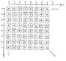
FIG. 30A shows an example of an image representing gray. The gray image shown in the figure is configured by arranging white data of 2 dots × 2 dots (represented by ◯ in the figure) and black data (represented by ● in the figure) in a checkered pattern. White data is RS = GS = BS = 1, and black data is RS = GS = BS = 0. FIG. 30B shows an example of the gradation conversion characteristics (DT = D) of the
[0071]
As shown in FIG. 31 (4), when the gradation conversion is performed after the smoothing process, the sum of the display levels of the R elements is 0.125 × 8 = 1, and the sum of the display levels of the G elements is 1 × 2 + 0. X2 = 2 and the total display level of the B element is 0.25x4 = 1. That is, the ratio of the display levels of the R, G, and B elements is 1: 2: 1, and the image to be displayed as an achromatic color is a greenish display image. As described above, when the
[0072]
FIG. 32 shows the output RS (FIG. 32 (1)) of the A / D converter 101 and the nonlinear gradation conversion when the
[0073]
As described above, the order of the smoothing process and the gradation conversion process is important. When the gradation characteristic of the image signal is converted, as shown in FIG. Must be provided in front of 1. With the above configuration, generation of false colors in the display image can be suppressed and gradation characteristics can be corrected.
The nonlinear gradation converter 36 uses an LUT (Look Up Table), but may be configured to calculate conversion data by calculation.
[0074]
When an element having a nonlinear electro-optical conversion characteristic such as CRT or LCD is used as the display element of the
[0075]
Display data DN output from the inverse
[0076]
As described above, when an element having nonlinear electro-optical conversion characteristics such as CRT or LCD is used as the display element of the
[0077]
The image display device (see FIG. 9) according to the second embodiment detects the high frequency detection values RH, GH, and BH based on the pixel data RS, GS, and BS, but the high frequency is based on the luminance data of the image data. Detection may be performed. FIG. 36 is a diagram showing the configuration of the image display device according to the present embodiment. The
[0078]
[Expression 2]
![]()
The
[0080]
In the second embodiment, as shown in FIG. 9, three high-
[0081]
FIG. 37 is a diagram showing the configuration of the image display device according to the present embodiment. The image display apparatus shown in the figure includes a plurality of terminals R1 to Rn, G1 to Gn, and B1 to Bn to which n types of image signals are input. From each terminal, an image signal having a different format such as a television image signal such as NTSC or Hi-Vision or an image signal output from a PC is input. The format of the image signal input to each terminal is set in advance, and the
[0082]
The
[0083]
According to the above configuration, by controlling the smoothing amount according to the format of the image signal, generation of false color is prevented in an image having a high frequency component, and deterioration of sharpness is suppressed in an image having a low frequency component. Therefore, a high-quality image can be displayed. Note that the display image content may be determined based on the format, and the smoothing coefficient may be controlled. For example, an image signal output from a PC contains a lot of high-frequency components because it contains a lot of character information and graphic information. On the other hand, the television signal includes image information such as a natural image or a moving image that is less likely to generate false colors. Therefore, based on the format of the selected image signal, it is determined whether the input image is an output image of a PC or a television image. In the case of a PC image, the generation of false colors is suppressed by increasing the smoothing amount. In the case of a television image, it may be configured to suppress the deterioration of sharpness by reducing the smoothing amount.
[0084]
FIG. 38 is a diagram showing a configuration of the image display device according to the present embodiment. An image signal of an arbitrary format is input to the
[0085]
The
[0086]
The conversion of the image size is performed by generating interpolated pixel data for interpolating the pixel data of the input image and converting the number of pixels. Therefore, when the enlargement process is performed, the sharpness of the contour portion is reduced in the enlarged image. As a result, the image subjected to the enlargement process has less high frequency components than the input image, and fewer false colors are generated. In particular, when the conversion magnification is 2 times or more, the sharpness of the contour portion in the enlarged image is greatly deteriorated. As described above, when an image is enlarged and displayed, it is necessary to suppress a decrease in the sharpness of the image rather than suppressing the occurrence of false colors. That is, in the case of an enlarged image, it is necessary not to perform smoothing or to reduce the smoothing amount. On the other hand, when the image is displayed in a reduced size, the high frequency component is increased and a false color is generated. Therefore, when displaying an image with a large reduction rate, it is necessary to increase the smoothing amount in accordance with the reduction rate. When the conversion magnification Z is large, the
[0087]
The
[0088]
As described above, when the size of the input image is converted and displayed according to the number of display elements constituting the display screen of the
[0089]
【The invention's effect】
An image display device and an image display method according to the present invention generate pixel data representing an input image corresponding to each display element with each display element serving as one pixel, and smooth pixel of pixel data representing a smoothed input image Data is calculated, the display level of each display element is calculated based on the smoothed pixel data and each color of each display element, and each display element is driven based on the calculated display level, thereby preventing the occurrence of false colors be able to.
[0090]
Further, since the high-frequency component of the input image is detected and the smoothing amount of the input image is controlled based on the detected amount, the generation of false colors can be prevented without causing deterioration of the sharpness in the contour portion.
[Brief description of the drawings]
FIG. 1 is a diagram illustrating a configuration of an image display device according to a first embodiment.
FIG. 2 is a diagram showing a configuration of a display device.
FIG. 3 is a diagram illustrating a configuration of a smoothing filter.
FIG. 4 is an explanatory diagram for explaining an operation of a smoothing filter.
FIG. 5 is a diagram illustrating an example of a smoothing coefficient.
6 is a diagram showing an example of a display image of the image display device according to
FIG. 7 is an explanatory diagram for explaining an operation of a smoothing filter.
FIG. 8 is a diagram illustrating an example of a smoothing coefficient.
FIG. 9 is a diagram illustrating a configuration of an image display device according to a second embodiment.
FIG. 10 is a diagram showing a configuration of a high-frequency detector.
FIG. 11 is an explanatory diagram for explaining the operation of the high-frequency detector.
FIG. 12 is a diagram illustrating a configuration of a high-frequency component calculator.
FIG. 13 is a diagram showing a configuration of a smoothing coefficient generator.
FIG. 14 is a diagram illustrating a configuration of a smoothing coefficient generator.
FIG. 15 is a diagram illustrating an example of characteristics of a smoothing coefficient.
FIG. 16 is a diagram showing another configuration of the smoothing coefficient generator.
FIG. 17 is a diagram illustrating an example of characteristics of a smoothing coefficient.
FIG. 18 is a diagram showing another configuration of the smoothing coefficient generator.
FIG. 19 is a diagram illustrating an example of characteristics of a smoothing coefficient.
FIG. 20 is a diagram showing another configuration of the high-frequency component calculator.
FIG. 21 is a diagram showing another configuration of the high-frequency component calculator.
FIG. 22 is a diagram showing another configuration of the high-frequency component calculator.
FIG. 23 is a diagram illustrating a configuration of an image display device according to a fifth embodiment.
FIG. 24 is a diagram illustrating a configuration of a smoothing filter.
FIG. 25 is a diagram showing a configuration of a high-frequency detector.
FIG. 26 is a diagram showing a configuration of an image display device according to a sixth embodiment.
FIG. 27 is a diagram showing a configuration of an image display device according to a seventh embodiment.
FIG. 28 is a diagram illustrating a configuration of a nonlinear gradation converter.
FIG. 29 is a diagram illustrating gradation conversion characteristics of a nonlinear gradation converter.
FIG. 30 is an explanatory diagram for explaining a gradation conversion operation;
FIG. 31 is an explanatory diagram for explaining a gradation conversion operation;
FIG. 32 is an explanatory diagram for explaining a gradation conversion operation;
FIG. 33 is a diagram showing a configuration of an image display device according to an eighth embodiment.
FIG. 34 is a diagram illustrating an example of gradation characteristics of a display device.
FIG. 35 is a diagram illustrating an example of gradation conversion characteristics of the inverse characteristic gradation converter.
FIG. 36 is a diagram illustrating a configuration of an image display device according to a ninth embodiment.
FIG. 37 is a diagram showing a structure of an image display device according to a tenth embodiment.
38 is a diagram showing a configuration of an image display device according to an eleventh embodiment. FIG.
FIG. 39 is a diagram illustrating a configuration of an image display device.
FIG. 40 is an explanatory diagram for describing a problem in a conventional image display device.
[Explanation of symbols]
1a, 1b, 1c, 51a, 51b, 51c Smoothing filter, 90, 91 Pixel data extraction means, 4 Weighted average calculator, 7a, 7b, 7c High frequency detector, 8, 8a, 8b, 8c Smoothing coefficient generator , 11 High frequency component calculator, 15, 1 50 Look-up table, 36a, 36b, 36c Non-linear gradation converter, 37 Inverse characteristic gradation converter, 39 Luminance calculator, 40 Signal switch, 41 Controller, 42 Image size detector, 43 Image size converter, 101a, 101b, 101c A / D converter, 102 display processor, 103, 104 display.
Claims (22)
前記R,G,Bの画像信号の各々を各表示素子に応じてサンプリングすることにより、R,G,Bの各色を表す単色画素データからなる画素データを、前記各表示素子に対応して生成する手段と、
前記画素データを構成する前記単色画素データの各々に平滑化処理を行うことにより平滑化された前記単色画素データからなる平滑化画素データを算出する手段と、
前記平滑化画素データを構成する前記単色画素データのいずれかを、前記表示素子の各表示色に応じて選択することにより、前記表示素子の表示レベルを示す表示データを出力する手段と、
前記表示データに基づいて前記各表示素子を駆動する手段とを備えたことを特徴とする画像表示装置。An image display device for displaying an image corresponding to an input image represented by R, G, B image signals on a display means configured by two-dimensionally arranging a plurality of display elements representing a plurality of colors. ,
The R, G, by sampling in accordance with the display elements each image signal of B, R, G, the pixel data consisting of a single color pixel data representing each color of B, and correspond to the respective display elements Means for generating;
Means for calculating a flat smoothed pixel data consisting of said single-color pixel data smoothed by performing a smoothing process on each of the monochrome pixel data constituting the pixel data,
Means for outputting display data indicating a display level of the display element by selecting any one of the single-color pixel data constituting the smoothed pixel data according to each display color of the display element;
An image display apparatus comprising: means for driving each display element based on the display data.
前記入力画像のサイズを変換する際の変換倍率に基づいて前記入力画像の平滑化量を制御することを特徴とする請求項1〜4のいずれか1項に記載の画像表示装置。Means for converting the size of the input image corresponding to the display size of the display means;
The image display apparatus according to any one of claims 1 to 4, characterized in that to control the amount of smoothing of the input image based on the conversion ratio in converting the size of the input image.
前記フォーマットに基づいて前記入力画像の平滑化量を制御することを特徴とする請求項1〜4のいずれか1項に記載の画像表示装置。Means for detecting the format of the input image;
The image display apparatus according to any one of claims 1 to 4, characterized in that to control the amount of smoothing of the input image based on the format.
前記R,G,Bの画像信号の各々を各表示素子に応じてサンプリングすることにより、R,G,Bの各色を表す単色画素データからなる画素データを、前記各表示素子に対応して生成し、
前記画素データを構成する前記単色画素データの各々に平滑化処理を行うことにより平滑化された前記単色画素データからなる平滑化画素データを算出し、
前記平滑化画素データを構成する前記単色画素データのいずれかを前記表示素子の各表示色に応じて選択することにより、前記表示素子の表示レベルを示す表示データを出力し、
前記表示データに基づいて前記各表示素子を駆動することにより前記画像の表示を行うことを特徴とする画像表示方法。An image display method for displaying an image corresponding to an input image represented by R, G, B image signals on a display means configured by two-dimensionally arranging a plurality of display elements representing a plurality of colors. ,
The R, G, by sampling in accordance with the display elements each image signal of B, R, G, the pixel data consisting of a single color pixel data representing each color of B, and correspond to the respective display elements Generate and
Calculates a flat smoothed pixel data consisting of said single-color pixel data smoothed by performing a smoothing process on each of the monochrome pixel data constituting the pixel data,
By selecting one of the single-color pixel data constituting the smoothed pixel data according to each display color of the display element, display data indicating the display level of the display element is output,
An image display method, wherein the image is displayed by driving each display element based on the display data.
前記入力画像のサイズを変換する際の変換倍率に基づいて前記入力画像の平滑化量を制御することを特徴とする請求項12〜15のいずれか1項に記載の画像表示方法。Convert the size of the input image corresponding to the display size of the display means,
The image display method according to any one of claims 12 to 1 5, characterized in that to control the amount of smoothing of the input image based on the conversion ratio in converting the size of the input image.
Priority Applications (2)
| Application Number | Priority Date | Filing Date | Title |
|---|---|---|---|
| JP2001080851A JP3852561B2 (en) | 2001-03-21 | 2001-03-21 | Image display device and image display method |
| US10/101,466 US6937256B2 (en) | 2001-03-21 | 2002-03-20 | Display device and image displaying method |
Applications Claiming Priority (1)
| Application Number | Priority Date | Filing Date | Title |
|---|---|---|---|
| JP2001080851A JP3852561B2 (en) | 2001-03-21 | 2001-03-21 | Image display device and image display method |
Publications (3)
| Publication Number | Publication Date |
|---|---|
| JP2002278500A JP2002278500A (en) | 2002-09-27 |
| JP2002278500A5 JP2002278500A5 (en) | 2005-10-27 |
| JP3852561B2 true JP3852561B2 (en) | 2006-11-29 |
Family
ID=18937058
Family Applications (1)
| Application Number | Title | Priority Date | Filing Date |
|---|---|---|---|
| JP2001080851A Expired - Lifetime JP3852561B2 (en) | 2001-03-21 | 2001-03-21 | Image display device and image display method |
Country Status (2)
| Country | Link |
|---|---|
| US (1) | US6937256B2 (en) |
| JP (1) | JP3852561B2 (en) |
Families Citing this family (14)
| Publication number | Priority date | Publication date | Assignee | Title |
|---|---|---|---|---|
| US6783900B2 (en) * | 2002-05-13 | 2004-08-31 | Micron Technology, Inc. | Color filter imaging array and method of formation |
| JP4451057B2 (en) | 2002-12-27 | 2010-04-14 | シャープ株式会社 | Display device driving method, display device, and program thereof |
| JP2005345678A (en) * | 2004-06-02 | 2005-12-15 | Mitsubishi Electric Corp | Portable display unit |
| US7733405B2 (en) * | 2005-02-10 | 2010-06-08 | Seiko Epson Corporation | Apparatus and method for resizing an image |
| JP4470901B2 (en) * | 2006-03-31 | 2010-06-02 | ソニー株式会社 | Imaging apparatus, high-frequency component detection circuit, high-frequency component detection method, and computer program |
| JP4569697B2 (en) * | 2008-01-08 | 2010-10-27 | 三菱電機株式会社 | Image processing apparatus, image display apparatus, and image processing method |
| US8422812B2 (en) | 2008-01-08 | 2013-04-16 | Mitsubishi Electric Corporation | Image processor and method therefor, and image display device |
| JP4503669B2 (en) * | 2008-09-26 | 2010-07-14 | シャープ株式会社 | Display device driving method, display device, and program thereof |
| US8502758B2 (en) * | 2009-12-10 | 2013-08-06 | Young Electric Sign Company | Apparatus and method for mapping virtual pixels to physical light elements of a display |
| JP2011147012A (en) * | 2010-01-15 | 2011-07-28 | Olympus Imaging Corp | Image display device, and method of displaying image |
| JP5983082B2 (en) * | 2012-06-21 | 2016-08-31 | セイコーエプソン株式会社 | Display control circuit, display device, and electronic device |
| CN105528990B (en) * | 2016-01-19 | 2019-04-09 | 西安诺瓦电子科技有限公司 | LED display uniformity correcting method |
| JP6927950B2 (en) * | 2018-11-30 | 2021-09-01 | パナソニック液晶ディスプレイ株式会社 | Display device |
| CN113296321B (en) * | 2020-02-21 | 2023-08-22 | 松下电器(美国)知识产权公司 | display device |
Family Cites Families (20)
| Publication number | Priority date | Publication date | Assignee | Title |
|---|---|---|---|---|
| JPS60120482A (en) * | 1983-12-02 | 1985-06-27 | Canon Inc | Picture signal processor |
| DE3855971T2 (en) * | 1987-11-16 | 1997-12-04 | Canon Kk | Image recorder |
| US5900982A (en) * | 1987-12-31 | 1999-05-04 | Projectavision, Inc. | High efficiency light valve projection system |
| US5300942A (en) * | 1987-12-31 | 1994-04-05 | Projectavision Incorporated | High efficiency light valve projection system with decreased perception of spaces between pixels and/or hines |
| JP2536094B2 (en) * | 1988-10-20 | 1996-09-18 | 富士ゼロックス株式会社 | Color image processing device |
| KR100202246B1 (en) * | 1989-02-27 | 1999-06-15 | 윌리엄 비. 켐플러 | Apparatus and method for digital video system |
| ATE137377T1 (en) * | 1990-02-06 | 1996-05-15 | Canon Kk | IMAGE PROCESSING DEVICE |
| US6246827B1 (en) * | 1990-08-17 | 2001-06-12 | Samsung Electronics Co., Ltd. | Deemphasis and subsequent reemphasis of high-energy reversed-spectrum components of a folded video signal |
| JP3200873B2 (en) * | 1990-11-30 | 2001-08-20 | ミノルタ株式会社 | Image processing device |
| US5818970A (en) * | 1991-04-26 | 1998-10-06 | Canon Kabushiki Kaisha | Image encoding apparatus |
| US5333243A (en) * | 1992-05-04 | 1994-07-26 | Hewlett-Packard Company | Method for forming color images, using a hue-plus-gray color model and error diffusion |
| US5603012A (en) * | 1992-06-30 | 1997-02-11 | Discovision Associates | Start code detector |
| US6072830A (en) * | 1996-08-09 | 2000-06-06 | U.S. Robotics Access Corp. | Method for generating a compressed video signal |
| JPH10319911A (en) * | 1997-05-15 | 1998-12-04 | Matsushita Electric Ind Co Ltd | Led display device and control method therefor |
| JPH118765A (en) * | 1997-06-16 | 1999-01-12 | Mitsubishi Electric Corp | Gradation lowering processing method, processor therefor integrated circuit for gradation lowering processing, and computer-readable recording medium recorded with gradation lowering program |
| US6611241B1 (en) * | 1997-12-02 | 2003-08-26 | Sarnoff Corporation | Modular display system |
| JP2000020025A (en) | 1998-07-01 | 2000-01-21 | Matsushita Electric Ind Co Ltd | Full-color light emitting diode panel display |
| US6816287B1 (en) * | 1998-07-17 | 2004-11-09 | Fuji Photo Film Co., Ltd. | Image reading apparatus and focusing control method |
| DE60141848D1 (en) * | 2000-11-02 | 2010-05-27 | Zygo Corp | METHOD AND DEVICE FOR HEAVY-ABBEASTING INTERFEROMETRY WITH PHASE DIFFERENTIAL ANALYSIS |
| JP2005011314A (en) * | 2003-05-23 | 2005-01-13 | Fujitsu Ltd | Image filter and image conversion method |
-
2001
- 2001-03-21 JP JP2001080851A patent/JP3852561B2/en not_active Expired - Lifetime
-
2002
- 2002-03-20 US US10/101,466 patent/US6937256B2/en not_active Expired - Lifetime
Also Published As
| Publication number | Publication date |
|---|---|
| US6937256B2 (en) | 2005-08-30 |
| US20020167465A1 (en) | 2002-11-14 |
| JP2002278500A (en) | 2002-09-27 |
Similar Documents
| Publication | Publication Date | Title |
|---|---|---|
| JP5296889B2 (en) | Image processing apparatus and image processing method | |
| JP4479709B2 (en) | Image display device, image display method, image display program, recording medium storing image display program, and electronic apparatus | |
| JP3852561B2 (en) | Image display device and image display method | |
| US6965389B1 (en) | Image displaying with multi-gradation processing | |
| KR100664572B1 (en) | Image signal correction method and image signal correction apparatus | |
| JP4967454B2 (en) | Image correction circuit, image correction method, and image display apparatus | |
| JP4635629B2 (en) | Sampling rate converter and image signal processing method | |
| JP2001343957A (en) | Liquid crystal display device | |
| US20070120869A1 (en) | Image display apparatus and method, program therefor, and recording medium having recorded thereon the same | |
| JPWO2007135822A1 (en) | Image processing apparatus, image processing method, program, recording medium, and integrated circuit | |
| JP2010122506A (en) | Image processing apparatus and image processing method | |
| JP5449468B2 (en) | Image processing method and image processing apparatus | |
| JP2010183232A (en) | Color gamut conversion device | |
| JP2003319411A (en) | Signal processor | |
| JPH11146349A (en) | Image converter and image conversion method | |
| US5894330A (en) | Adaptive anti-flicker method for VGA to TV data conversion | |
| JP4047859B2 (en) | Color correction apparatus and method for flat panel display device | |
| JP2002132225A (en) | Video signal corrector and multimedia computer system using the same | |
| JP4397623B2 (en) | Tone correction device | |
| JP3661925B2 (en) | Video signal processing circuit and method for display device | |
| JP2002142132A (en) | Apparatus and method for correcting image data | |
| JP4305917B2 (en) | Video signal processing apparatus and television apparatus | |
| JP2007324665A (en) | Image correction apparatus and video display apparatus | |
| JP3912079B2 (en) | Error diffusion processing circuit and method for display device | |
| JP5311443B2 (en) | Color image display device and monochrome image display method |
Legal Events
| Date | Code | Title | Description |
|---|---|---|---|
| RD01 | Notification of change of attorney |
Free format text: JAPANESE INTERMEDIATE CODE: A7421 Effective date: 20040708 |
|
| A521 | Written amendment |
Free format text: JAPANESE INTERMEDIATE CODE: A523 Effective date: 20050713 |
|
| A621 | Written request for application examination |
Free format text: JAPANESE INTERMEDIATE CODE: A621 Effective date: 20050713 |
|
| A871 | Explanation of circumstances concerning accelerated examination |
Free format text: JAPANESE INTERMEDIATE CODE: A871 Effective date: 20050713 |
|
| A975 | Report on accelerated examination |
Free format text: JAPANESE INTERMEDIATE CODE: A971005 Effective date: 20050928 |
|
| A131 | Notification of reasons for refusal |
Free format text: JAPANESE INTERMEDIATE CODE: A131 Effective date: 20060124 |
|
| A521 | Written amendment |
Free format text: JAPANESE INTERMEDIATE CODE: A523 Effective date: 20060324 |
|
| TRDD | Decision of grant or rejection written | ||
| A01 | Written decision to grant a patent or to grant a registration (utility model) |
Free format text: JAPANESE INTERMEDIATE CODE: A01 Effective date: 20060816 |
|
| A61 | First payment of annual fees (during grant procedure) |
Free format text: JAPANESE INTERMEDIATE CODE: A61 Effective date: 20060829 |
|
| R151 | Written notification of patent or utility model registration |
Ref document number: 3852561 Country of ref document: JP Free format text: JAPANESE INTERMEDIATE CODE: R151 |
|
| FPAY | Renewal fee payment (event date is renewal date of database) |
Free format text: PAYMENT UNTIL: 20090915 Year of fee payment: 3 |
|
| FPAY | Renewal fee payment (event date is renewal date of database) |
Free format text: PAYMENT UNTIL: 20100915 Year of fee payment: 4 |
|
| FPAY | Renewal fee payment (event date is renewal date of database) |
Free format text: PAYMENT UNTIL: 20110915 Year of fee payment: 5 |
|
| FPAY | Renewal fee payment (event date is renewal date of database) |
Free format text: PAYMENT UNTIL: 20110915 Year of fee payment: 5 |
|
| FPAY | Renewal fee payment (event date is renewal date of database) |
Free format text: PAYMENT UNTIL: 20120915 Year of fee payment: 6 |
|
| FPAY | Renewal fee payment (event date is renewal date of database) |
Free format text: PAYMENT UNTIL: 20130915 Year of fee payment: 7 |
|
| R250 | Receipt of annual fees |
Free format text: JAPANESE INTERMEDIATE CODE: R250 |
|
| R250 | Receipt of annual fees |
Free format text: JAPANESE INTERMEDIATE CODE: R250 |
|
| R250 | Receipt of annual fees |
Free format text: JAPANESE INTERMEDIATE CODE: R250 |
|
| R250 | Receipt of annual fees |
Free format text: JAPANESE INTERMEDIATE CODE: R250 |
|
| R250 | Receipt of annual fees |
Free format text: JAPANESE INTERMEDIATE CODE: R250 |
|
| R250 | Receipt of annual fees |
Free format text: JAPANESE INTERMEDIATE CODE: R250 |
|
| EXPY | Cancellation because of completion of term |