JP3846397B2 - Biochip with confocal optics - Google Patents
Biochip with confocal optics Download PDFInfo
- Publication number
- JP3846397B2 JP3846397B2 JP2002301288A JP2002301288A JP3846397B2 JP 3846397 B2 JP3846397 B2 JP 3846397B2 JP 2002301288 A JP2002301288 A JP 2002301288A JP 2002301288 A JP2002301288 A JP 2002301288A JP 3846397 B2 JP3846397 B2 JP 3846397B2
- Authority
- JP
- Japan
- Prior art keywords
- light
- sample
- biochip
- substrate
- lens
- Prior art date
- Legal status (The legal status is an assumption and is not a legal conclusion. Google has not performed a legal analysis and makes no representation as to the accuracy of the status listed.)
- Expired - Fee Related
Links
Images


Landscapes
- Investigating, Analyzing Materials By Fluorescence Or Luminescence (AREA)
- Microscoopes, Condenser (AREA)
Description
【0001】
【発明の属する技術分野】
本発明は、微弱な光の進行方向を所定の方向に制御する機能を有するバイオチップに関し、具体的には共焦点光学系を備えたバイオチップに関する。また本発明は、当該バイオチップを用いたバイオチップ読取装置および光検出方法に関する。
【0002】
【従来の技術】
ガラスやシリコンなどの基板上に複数の試料を並べて固定化したバイオチップ(DNAチップ、プロテインチップ、DNAアレイおよびDNAマイクロアレイなどを含む)を用いた物性評価試験や定量試験では、蛍光あるいは化学発光の検出が行われることが多い。こうした微弱な光を検出する代表的な装置としては、共焦点光学系を用いたバイオチップ読取装置が挙げられる(例えば、特許文献1を参照のこと)。
【0003】
共焦点光学系とは、結像する位置(合焦点位置)にピンホールを置くことで、合焦点以外からの光を一切排除し、コントラストの良い像を得るための光学系である。
【0004】
共焦点光学系を用いた従来のバイオチップ読取装置22は、図6に示すように、試料23を備えたバイオチップ24、対物レンズ25、ビームスプリッター26、ミラー27、光学フィルタ28、受光レンズ29、共焦点ピンホール30、受光器31などから構成される。光源(図示されない)から出射される励起光32をビームスプリッター26で反射させて試料23に照射すると、励起された試料23から蛍光33が発生する。その蛍光33を、試料23の上側に位置する対物レンズ25で取り込み、ビームスプリッター26を透過させ、ミラー27により光学フィルタ28に導き、受光レンズ29により集光し、共焦点ピンホール30によりノイズ光を除去して、受光器31により検出する。化学発光検出の場合、励起光32は照射されないが、試料23から発せられた光が受光器31により検出されるまでの過程は同様である。
このような共焦点型のバイオチップ読取装置は、検出光のSN比が高いが、ノイズ光を低減させるための光学系が複雑かつ大型なので装置価格が高い。
【0005】
【特許文献1】
特開2001−311690「バイオチップ読取装置及び電気泳動装置」
【発明が解決しようとする課題】
上述の事情に鑑み、本発明は、バイオチップ読取装置の小型化および低価格化を目的とする。
【0006】
【課題を解決するための手段】
本発明にかかるバイオチップは、複数の試料を備えた基板と、前記基板の前記試料が備えられた面とは反対側の面に設けられた遮光部材とを有するバイオチップであって、前記基板は、前記試料の各々に対応したレンズを備えており、前記遮光部材は、前記試料の各々に対応する開口を有し、前記試料と前記開口とが前記レンズを介して共焦点の関係にあることを特徴とする。
このような構成のバイオチップは、事実上チップ内に共焦点光学系を有しているので、バイオチップ読取装置の複雑かつ大型な光学系を要しない。すなわち、上記バイオチップにより、基板上の励起された試料から発生した光のうち基板側に出射した光を、レンズにより集光させ、試料の各々に対応するように遮光部材上に設けた開口を通過させることができる。従って、上記バイオチップを用いて、励起光の照射と試料が発生する光の検出とを、基板を挟んで反対側で行うようにすれば、バイオチップ読取装置の小型化および低価格化が可能となる。
【0007】
前記基板は、屈折率の異なる複数の物質を積層して形成しても良い。
このように基板を形成することで、内部にレンズ機能を有する基板を容易に形成することができる。
また、前記基板を形成する複数の物質のうち、前記試料と接する物質の屈折率を、前記試料の屈折率より大きくすると良い。
このように、試料と接する基板の材質として試料よりも屈折率が大きなものを選べば、試料から発生して基板側に進行する蛍光は基板の光入射面に対して法線の方向に屈折するため、基板と反対側に発生する蛍光よりも集光効率が良い。
【0008】
前記基板の前記試料が備えられた面側には、前記試料を挟んで第1マイクロレンズアレイがさらに形成されており、前記第1マイクロレンズアレイは、前記試料の各々に対応する第1レンズを有し、前記第1レンズの焦点が前記試料の位置に一致するようにしても良い。
このように、バイオチップが第1マイクロレンズアレイを備えることで、光源からの光を試料に集光するための対物レンズが不要となり、装置を小型化することができる。
さらに、このような構成により励起光を各試料に効率良く集光することができるので、複数の試料を同時に精度良く励起することができる。
【0009】
前記基板の前記試料が備えられた面とは反対側の面に、前記遮光部材を挟んで、第2マイクロレンズアレイが配置されており、前記第2マイクロレンズアレイは、前記開口の各々に対応する第2レンズを有し、前記第2レンズの焦点は前記開口の位置に一致するようにしても良い。
このように、バイオチップが第2マイクロレンズアレイを備えることで、遮光部材の開口を通過した光を受光する受光レンズが不要となり、装置を小型化することができる。
さらに、このような構成により各試料が発生した光を効率良く集光することができるので、複数の試料が発生する光を同時に精度良く検出することができる。
【0010】
前記試料は、生物の遺伝情報を含んでいても良い。
生物の遺伝情報を含む試料を備えたバイオチップを用いることで、遺伝子配列の決定、特定遺伝子の有無の確認、SNP(単一塩基多型)の解析、タンパク質の同定または機能解析などを行うことができる。
【0011】
本発明のバイオチップ読取装置は、光源と、光源からの励起光を試料に集光するための対物レンズと、バイオチップと、前記試料から前記基板側に発生して前記遮光部材の前記開口を通過した光を受光するための受光レンズと、前記励起光を遮断もしくは減衰させるための光学フィルタと、前記受光レンズおよび前記光学フィルタを通過した光を受光する受光器とからなり、前記バイオチップは、複数の試料を備えた基板と、前記基板の前記試料が備えられた面とは反対側の面に設けられた遮光部材とを有するバイオチップであって、前記基板は、前記試料の各々に対応したレンズを備えており、前記遮光部材は、前記試料の各々に対応する開口を有し、前記試料と前記開口とが前記レンズを介して共焦点の関係にあることを特徴とする。
このような構成のバイオチップ読取装置は、バイオチップ内に共焦点光学系を有するので、従来の装置に比べて小型で低価格である。
【0012】
本発明にかかる光検出方法は、上記バイオチップと、光源と、受光器とを用いた光検出方法であって、前記光源からの励起光を前記試料に照射することにより前記試料から発生した光のうち、前記基板側に出射した光を、前記レンズにより集光し、前記試料の各々に対応するように前記遮光部材上に設けた開口を通過させて受光器により検出することを特徴とする。
このように、共焦点光学系を備えたバイオチップを用いて、励起光の照射と試料が発生する光の検出とを、基板を挟んで反対側で行うことにより、従来の光検出装置のような複雑な光学系が不要となり、装置を小型化することができる。
【0013】
上記光検出方法において、前記光源から励起光の照射を停止したのち、前記受光器による光検出を行っても良い。
このように、励起光の照射を停止した状態で試料が発生する光の検出を行うことにより、励起光がノイズ光として検出されることはないので、SN比が飛躍的に向上する。
【0014】
【詳細な説明】
以下、本発明の好適な実施形態を、蛍光を検出する場合を例に、図面を参照しながら詳しく説明する。但し、この実施形態に記載されている構成部品の寸法、材質、形状、その相対的配置などは説明例に過ぎず、特に記載がない限りこの発明の範囲をそれらに限定する意図はない。また、各図面は模式図であり、構成要素の屈折率の相異を考慮して描かれてはいない。
【0015】
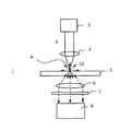
図1は、本発明の一つの実施形態にかかるバイオチップ読取装置1を示す。バイオチップ読取装置1は、光源2、対物レンズ4、バイオチップ5、受光レンズ6、光学フィルタ7、および受光器8から構成される。
【0016】
まず、図2により、バイオチップ読取装置1で使用されるバイオチップ5aの細部を説明する。バイオチップ5aにおいて、基板11は、屈折率の異なる物質12および13から形成され、基板11の表面上には試料9が備えられている。ここで、物質12と13との境界面は、試料9の各々に対応したレンズ120を有するマイクロレンズアレイを形成している。望ましくは、各レンズ120の有効半径は試料の配置間隔に等しい。さらに、基板11の試料9が備えられた面とは反対側の面には遮光部材14が形成され、遮光部材14には各試料に対応した開口15が設けられている。ここで、試料9と開口15は、物質12および13から形成されるマイクロレンズアレイを介して共焦点の関係にある。
【0017】
次に、バイオチップ読取装置1の動作を説明する。光源2からの励起光3は、対物レンズ4で集束されて、基板11上の試料9に照射される。試料9は励起光3を吸収して、蛍光10を発生する。蛍光10は、励起光3とは異なる波長特性を有する。試料9から発生した蛍光10は、バイオチップ5a内に物質12および13により形成されたマイクロレンズアレイによって屈折作用を受ける。このとき、試料9と開口15は共焦点の関係にあるので、蛍光10は遮光部材14の開口15を通過する。ここで、励起光3も同様にレンズの屈折作用によって開口15を通過するので、受光レンズ6と受光器8との間に波長選択特性を有する光学フィルタ7を設け、蛍光10を透過させ、励起光3を透過させないようにする。光学フィルタ7を透過した蛍光10は、受光器8で検出される。
ここで、光学フィルタとは、特定の波長の光を透過させるかまたは吸収もしくは反射することにより遮断する機能を有する波長選択素子をいう。
【0018】
このように、本発明のバイオチップは、従来のバイオチップと違い、試料から発生した蛍光のうち基板側に発生した蛍光を検出するための構成となっている。図6に示すような従来の共焦点型バイオチップ読取装置を用いて基板と反対側に発生する蛍光を検出する場合、検出される光の量は、対物レンズ25の開口数(NA)に依存してわずかである。一方、本発明に従って基板側に発生した蛍光を検出する場合、基板の材質として試料よりも屈折率が大きなものを選べば、基板側に進行する蛍光は基板の光入射面に対して法線の方向に屈折するため、基板と反対側に発生する蛍光よりも効率良く集光することができる。
ここで、試料の屈折率は1.33〜1.50程度であるから、例えば、試料の屈折率が1.4であるとき、基板の材料として屈折率が1.6程度の樹脂を選択すれば、蛍光の屈折角は約60度となり、集光効率が良い。従って、基板に用いる材料としては、透明で屈折率が大きなガラスや樹脂などが相応しい。
【0019】
基板内部に形成するレンズの曲率および基板の厚みは、試料および基板の屈折率に応じて、蛍光の集光効率が最適となるように選択される。
【0020】
基板11は、屈折率の異なる複数の樹脂により形成されても良いし、樹脂層と空気層とで形成されても良い。空気の屈折率は1であるから、屈折率の大きな樹脂層を組み合わせるとNAの大きなレンズを形成することができ、より多くの蛍光を検出することができる。
【0021】
図3は、本発明にかかる別のバイオチップ5bを示す。図3に示すように、基板11は、2つ以上のマイクロレンズアレイを光軸方向に積層した構成であっても良い。ここで、物質16および18の屈折率は同じであっても良いし、異なっていても良い。
このように2つ以上のマイクロレンズアレイを積層することにより、レンズの合成NAを大きくすることができるので、より多くの蛍光を検出することができる。
【0022】
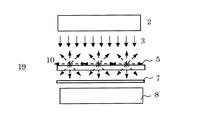
図4は、本発明のさらに別の実施形態にかかるバイオチップ読取装置19を示す。バイオチップ読取装置19は、バイオチップが備える複数の試料に一度に励起光を照射し、各試料が発生した光を同時に検出することを特徴とする。図5に、バイオチップ読取装置19に使用されるバイオチップ5cの細部を示す。
【0023】
バイオチップ5cは、バイオチップ5bの構成に加えて、基板11の試料10が備えられた面側にスペーサ21を介して第1マイクロレンズアレイ20を備える。ここで、第1マイクロレンズアレイ20は、試料の各々に対応する第1レンズ200を有し、第1レンズ200の焦点は前記試料の位置に一致する。
【0024】
このように、バイオチップ5cが第1マイクロレンズアレイ20を備えることで、光源からの励起光3を試料に集光するための対物レンズが不要となる。即ち、第1マイクロレンズアレイ20により、励起光3は各試料10の位置に効率良く集光されるので、複数の試料10を同時に精度良く励起することができる。対物レンズを用いる場合には、焦点位置を各試料に合わせる必要があるが、第1マイクロレンズアレイ20が備えられている場合は、第1レンズ200の焦点が各試料の位置に一致しているので焦点位置を調節する必要がない。
【0025】
さらに、図示しないが、基板の試料が備えられた面とは反対側の面に、遮光部材を挟んで第2マイクロレンズアレイを備えても良い。第2マイクロレンズアレイは、遮光部材の開口の各々に対応する第2レンズを有し、第2レンズの焦点は前記開口の位置に一致するようにする。
このように、バイオチップ5cが第2マイクロレンズアレイを備えることで、各試料が発生した光は効率良く集光されるので、複数の試料が発生する光を同時に精度良く検出することができる。受光器としては高感度CCDカメラなどが用いられる。
【0026】
従って、バイオチップ5cを用いれば、複数の試料を同時に励起し、複数の試料が発生する光を同時に検出することができるので、基板を走査する必要がない。
ただし、バイオチップ5bに第1マイクロレンズアレイ20および第2マイクロレンズアレイを設ける際には、精度の高い位置合わせが必要である。位置合わせにはアラインメントマークを用いる。
【0027】
第1マイクロレンズアレイ20の第1レンズ200は、空気と接触していても良いが、屈折率の異なる樹脂を用いてレンズ表面を平坦化しても良い。そうすれば、レンズ表面を粉塵から保護することができると同時に取り扱いが容易となる。
【0028】
以上の実施例においては、基板が備えるレンズとして、屈折率の異なる複数の物質を積層して形成したマイクロレンズアレイの例を示したが、屈折率分布型レンズ(GRINレンズ)を配列したGRINレンズアレイとしても同様の効果が得られる。
【0029】
本発明にかかる光検出方法は、以上で説明したバイオチップと、光源と、受光器とを用いた光検出方法であって、光源からの励起光を試料に照射し、励起された試料から発生した光のうち、基板側に出射した光を、チップ内部のレンズにより集光し、試料の各々に対応するように遮光部材上に設けた開口を通過させて受光器により検出することを特徴とする。
このように、共焦点光学系を備えたバイオチップを用いて、励起光の照射と試料が発生する光の検出とを、基板を挟んで反対側で行うことにより、従来の光検出装置のような複雑な光学系が不要となり、装置を小型化することができる。
【0030】
さらに、上記光検出方法において、光源からの励起光の照射を停止したのち、受光器による光検出を行えば、励起光がノイズ光として検出されることはないので、SN比が飛躍的に向上する。また、光検出装置において励起光を除去するための光学フィルタは不要となり、装置を小型化することができる。
【0031】
以上、蛍光を検出する場合を例に説明したが、化学発光を検出する場合においても本発明にかかるバイオチップにより同様の効果が得られることは明白である。
【0032】
本発明の光検出方法は、遺伝子配列の決定、特定遺伝子の有無の確認、特定遺伝子の発現レベルの測定、SNP(単一塩基多型)の解析、実験用マウスに投与した物質の代謝・吸収・排泄の経路または状態の確認、細胞内のイオン濃度測定、タンパク質の同定または機能解析などに用いることができる。また、個人の健康状態を判別する健康診断や個人セキュリティーのための検査などにも応用することができる。
【発明の効果】
本発明にかかるバイオチップは、例えば、複数の試料を備える基板を屈折率の異なる物質を積層して形成することで、基板にレンズ機能を持たせている。さらに、基板の試料が備えられた面とは反対側の面に、試料の各々に対応する開口を有する遮光部材を設けることでチップ内部に共焦点光学系を備える構成とした。本発明のバイオチップを用いて、励起光の照射と試料が発生する光の検出とを、基板を挟んで反対側で行えば、従来の複雑かつ大型な光学系が不要となり、バイオチップ読取装置の小型化および低価格化が可能となる。
【図面の簡単な説明】
【図1】 本発明の実施形態にかかるバイオチップ読取装置を示す。
【図2】 本発明の実施形態にかかるバイオチップ読取装置の要部を示す。
【図3】 本発明の別の実施形態にかかるバイオチップを示す。
【図4】 本発明の別の実施形態にかかるバイオチップ読取装置を示す。
【図5】 本発明の別の実施形態にかかるバイオチップ読取装置の要部を示す。
【図6】 従来の共焦点型バイオチップ読取装置を示す。
【符号の説明】
1、19、22 バイオチップ読取装置
2 光源
3、32 励起光
4、25 対物レンズ
5、24 バイオチップ
6、29 受光レンズ
7、28 光学フィルタ
8、31 受光器
9、23 試料
10、33 蛍光
11 基板
14 遮光部材
15 開口
20 第1マイクロレンズアレイ
21 スペーサ
26 ピームスプリッタ
27 ミラー
30 共焦点ピンホール
120 レンズ
200 第1レンズ[0001]
BACKGROUND OF THE INVENTION
The present invention relates to a biochip having a function of controlling a weak light traveling direction in a predetermined direction, and more specifically to a biochip including a confocal optical system. The present invention also relates to a biochip reader and a light detection method using the biochip.
[0002]
[Prior art]
In physical property evaluation tests and quantitative tests using biochips (including DNA chips, protein chips, DNA arrays, DNA microarrays, etc.) in which multiple samples are arranged and immobilized on a substrate such as glass or silicon, fluorescence or chemiluminescence Detection is often performed. A typical device for detecting such weak light includes a biochip reader using a confocal optical system (see, for example, Patent Document 1).
[0003]
A confocal optical system is an optical system for obtaining an image with good contrast by placing a pinhole at a position where an image is formed (focused position), thereby eliminating any light from other than the focused position.
[0004]
As shown in FIG. 6, a
Such a confocal biochip reader has a high S / N ratio of detection light, but the cost of the apparatus is high because the optical system for reducing noise light is complex and large.
[0005]
[Patent Document 1]
JP 2001-31690 “Biochip reader and electrophoresis apparatus”
[Problems to be solved by the invention]
In view of the above circumstances, an object of the present invention is to reduce the size and price of a biochip reader.
[0006]
[Means for Solving the Problems]
A biochip according to the present invention is a biochip having a substrate provided with a plurality of samples and a light shielding member provided on a surface of the substrate opposite to the surface provided with the samples. Includes a lens corresponding to each of the samples, and the light shielding member has an opening corresponding to each of the samples, and the sample and the opening are in a confocal relationship via the lens. It is characterized by that.
Since the biochip having such a configuration actually has a confocal optical system in the chip, a complicated and large optical system of the biochip reader is not required. That is, the light emitted from the excited sample on the substrate to the substrate side by the biochip is condensed by the lens, and an opening provided on the light shielding member so as to correspond to each of the samples. Can be passed. Therefore, if the biochip is used to irradiate the excitation light and detect the light generated by the sample on the opposite side of the substrate, the biochip reader can be reduced in size and cost. It becomes.
[0007]
The substrate may be formed by stacking a plurality of substances having different refractive indexes.
By forming the substrate in this way, a substrate having a lens function can be easily formed inside.
Moreover, it is preferable that a refractive index of a substance in contact with the sample among a plurality of substances forming the substrate is larger than a refractive index of the sample.
Thus, if a material having a higher refractive index than the sample is selected as the material of the substrate in contact with the sample, the fluorescence generated from the sample and traveling to the substrate side is refracted in the direction normal to the light incident surface of the substrate. Therefore, the light collection efficiency is better than the fluorescence generated on the side opposite to the substrate.
[0008]
A first microlens array is further formed on the surface side of the substrate on which the sample is provided, with the sample interposed therebetween, and the first microlens array has a first lens corresponding to each of the samples. And the focal point of the first lens may coincide with the position of the sample.
Thus, since the biochip includes the first microlens array, an objective lens for condensing light from the light source onto the sample becomes unnecessary, and the apparatus can be downsized.
Furthermore, since the excitation light can be efficiently collected on each sample by such a configuration, a plurality of samples can be excited simultaneously with high accuracy.
[0009]
A second microlens array is disposed on a surface of the substrate opposite to the surface on which the sample is provided, with the light shielding member interposed therebetween, and the second microlens array corresponds to each of the openings. The second lens may be provided, and the focal point of the second lens may coincide with the position of the opening.
As described above, since the biochip includes the second microlens array, a light receiving lens that receives light that has passed through the opening of the light shielding member is not required, and the apparatus can be miniaturized.
Further, since the light generated by each sample can be efficiently collected with such a configuration, the light generated by a plurality of samples can be detected simultaneously with high accuracy.
[0010]
The sample may contain genetic information of the organism.
By using a biochip equipped with a sample containing genetic information of organisms, determination of gene sequence, confirmation of the presence or absence of a specific gene, analysis of SNP (single nucleotide polymorphism), protein identification or functional analysis, etc. Can do.
[0011]
The biochip reader of the present invention includes a light source, an objective lens for condensing excitation light from the light source on the sample, a biochip, and the opening of the light shielding member generated from the sample on the substrate side. The biochip comprises: a light receiving lens for receiving light that has passed; an optical filter for blocking or attenuating the excitation light; and a light receiver for receiving light that has passed through the light receiving lens and the optical filter. A biochip having a substrate provided with a plurality of samples and a light shielding member provided on a surface of the substrate opposite to the surface provided with the samples, wherein the substrate is provided on each of the samples. A corresponding lens is provided, and the light shielding member has an opening corresponding to each of the samples, and the sample and the opening are in a confocal relationship through the lens.
Since the biochip reader having such a configuration has a confocal optical system in the biochip, it is smaller and less expensive than the conventional apparatus.
[0012]
A light detection method according to the present invention is a light detection method using the biochip, a light source, and a light receiver, and light generated from the sample by irradiating the sample with excitation light from the light source. Among these, the light emitted to the substrate side is collected by the lens, and detected by a light receiver through an opening provided on the light shielding member so as to correspond to each of the samples. .
In this way, using a biochip equipped with a confocal optical system, the irradiation of excitation light and the detection of light generated by the sample are performed on the opposite side across the substrate, so that the conventional photodetection device is used. A complicated optical system becomes unnecessary, and the apparatus can be miniaturized.
[0013]
In the light detection method, light detection by the light receiver may be performed after the irradiation of excitation light from the light source is stopped.
Thus, by detecting the light generated by the sample in a state where the irradiation of the excitation light is stopped, the excitation light is not detected as noise light, and the SN ratio is dramatically improved.
[0014]
[Detailed explanation]
Hereinafter, a preferred embodiment of the present invention will be described in detail with reference to the drawings, taking the case of detecting fluorescence as an example. However, the dimensions, materials, shapes, relative arrangements, and the like of the components described in this embodiment are merely illustrative examples, and the scope of the present invention is not intended to be limited to these unless otherwise specified. Each drawing is a schematic diagram and is not drawn in consideration of the difference in refractive index of the constituent elements.
[0015]
FIG. 1 shows a
[0016]
First, details of the
[0017]
Next, the operation of the
Here, the optical filter refers to a wavelength selection element having a function of transmitting light of a specific wavelength or blocking it by absorbing or reflecting.
[0018]
Thus, unlike the conventional biochip, the biochip of the present invention is configured to detect the fluorescence generated on the substrate side among the fluorescence generated from the sample. When detecting fluorescence generated on the opposite side of the substrate using a conventional confocal biochip reader as shown in FIG. 6, the amount of light detected depends on the numerical aperture (NA) of the
Here, since the refractive index of the sample is about 1.33 to 1.50, for example, when the refractive index of the sample is 1.4, a resin having a refractive index of about 1.6 is selected as the substrate material. For example, the refraction angle of fluorescence is about 60 degrees, and the light collection efficiency is good. Accordingly, glass or resin having a high refractive index is suitable as a material used for the substrate.
[0019]
The curvature of the lens formed in the substrate and the thickness of the substrate are selected so as to optimize the fluorescence condensing efficiency according to the refractive index of the sample and the substrate.
[0020]
The
[0021]
FIG. 3 shows another
By stacking two or more microlens arrays in this way, the combined NA of the lenses can be increased, so that more fluorescence can be detected.
[0022]
FIG. 4 shows a
[0023]
In addition to the configuration of the
[0024]
Thus, since the
[0025]
Further, although not shown, a second microlens array may be provided on a surface opposite to the surface on which the sample of the substrate is provided with a light shielding member interposed therebetween. The second microlens array has a second lens corresponding to each of the openings of the light shielding member, and the focal point of the second lens is made to coincide with the position of the opening.
As described above, since the
[0026]
Therefore, if the
However, when the
[0027]
The
[0028]
In the above embodiments, an example of a microlens array formed by laminating a plurality of substances having different refractive indexes has been shown as a lens included in the substrate. However, a GRIN lens in which refractive index distribution lenses (GRIN lenses) are arranged is shown. The same effect can be obtained as an array.
[0029]
The light detection method according to the present invention is a light detection method using the biochip described above, a light source, and a light receiver, and is generated from the excited sample by irradiating the sample with excitation light from the light source. The light emitted to the substrate side is collected by the lens inside the chip and is detected by the light receiver through the opening provided on the light shielding member so as to correspond to each of the samples. To do.
In this way, using a biochip equipped with a confocal optical system, the irradiation of excitation light and the detection of light generated by the sample are performed on the opposite side across the substrate, so that the conventional photodetection device is used. A complicated optical system becomes unnecessary, and the apparatus can be miniaturized.
[0030]
Furthermore, in the above-described light detection method, if the light detection by the light receiver is performed after the irradiation of the excitation light from the light source is stopped, the excitation light is not detected as noise light, so the SN ratio is greatly improved. To do. In addition, an optical filter for removing excitation light in the light detection device is not necessary, and the device can be miniaturized.
[0031]
Although the case where fluorescence is detected has been described above as an example, it is obvious that the same effect can be obtained by the biochip according to the present invention even when chemiluminescence is detected.
[0032]
The light detection method of the present invention includes determination of gene sequence, confirmation of the presence or absence of a specific gene, measurement of the expression level of a specific gene, analysis of SNP (single nucleotide polymorphism), metabolism / absorption of a substance administered to an experimental mouse. -It can be used for confirmation of the route or state of excretion, measurement of intracellular ion concentration, protein identification or functional analysis. In addition, it can be applied to a health check for determining an individual's health condition and a test for personal security.
【The invention's effect】
In the biochip according to the present invention, for example, a substrate having a plurality of samples is formed by laminating substances having different refractive indexes, so that the substrate has a lens function. Further, a confocal optical system is provided inside the chip by providing a light shielding member having an opening corresponding to each of the samples on the surface of the substrate opposite to the surface on which the sample is provided. By using the biochip of the present invention to perform excitation light irradiation and detection of light generated by a sample on the opposite side across the substrate, a conventional complicated and large optical system becomes unnecessary, and a biochip reader Can be reduced in size and price.
[Brief description of the drawings]
FIG. 1 shows a biochip reader according to an embodiment of the present invention.
FIG. 2 shows a main part of a biochip reader according to an embodiment of the present invention.
FIG. 3 shows a biochip according to another embodiment of the present invention.
FIG. 4 shows a biochip reader according to another embodiment of the present invention.
FIG. 5 shows a main part of a biochip reader according to another embodiment of the present invention.
FIG. 6 shows a conventional confocal biochip reader.
[Explanation of symbols]
1, 19, 22
Claims (8)
前記基板は、前記試料の各々に対応したレンズを備えており、
前記遮光部材は、前記試料の各々に対応する開口を有し、
前記試料と前記開口とが前記レンズを介して共焦点の関係にあることを特徴とする、バイオチップ。A biochip having a substrate provided with a plurality of samples, and a light shielding member provided on a surface of the substrate opposite to the surface provided with the samples,
The substrate includes a lens corresponding to each of the samples,
The light shielding member has an opening corresponding to each of the samples,
A biochip, wherein the sample and the aperture are in a confocal relationship through the lens.
前記第1マイクロレンズアレイは、前記試料の各々に対応する第1レンズを有し、
前記第1レンズの焦点は前記試料の位置に一致することを特徴とする、請求項1に記載のバイオチップ。A first microlens array is arranged on the surface side of the substrate on which the sample is provided, with the sample interposed therebetween,
The first microlens array has a first lens corresponding to each of the samples,
The biochip according to claim 1, wherein a focal point of the first lens coincides with a position of the sample.
Priority Applications (1)
| Application Number | Priority Date | Filing Date | Title |
|---|---|---|---|
| JP2002301288A JP3846397B2 (en) | 2002-10-16 | 2002-10-16 | Biochip with confocal optics |
Applications Claiming Priority (1)
| Application Number | Priority Date | Filing Date | Title |
|---|---|---|---|
| JP2002301288A JP3846397B2 (en) | 2002-10-16 | 2002-10-16 | Biochip with confocal optics |
Publications (2)
| Publication Number | Publication Date |
|---|---|
| JP2004138420A JP2004138420A (en) | 2004-05-13 |
| JP3846397B2 true JP3846397B2 (en) | 2006-11-15 |
Family
ID=32449670
Family Applications (1)
| Application Number | Title | Priority Date | Filing Date |
|---|---|---|---|
| JP2002301288A Expired - Fee Related JP3846397B2 (en) | 2002-10-16 | 2002-10-16 | Biochip with confocal optics |
Country Status (1)
| Country | Link |
|---|---|
| JP (1) | JP3846397B2 (en) |
Families Citing this family (12)
| Publication number | Priority date | Publication date | Assignee | Title |
|---|---|---|---|---|
| JP4581498B2 (en) * | 2004-06-15 | 2010-11-17 | カシオ計算機株式会社 | Biopolymer analysis chip |
| JP4500612B2 (en) | 2004-07-09 | 2010-07-14 | 横河電機株式会社 | Biochip reader |
| JP2006058044A (en) | 2004-08-18 | 2006-03-02 | Yokogawa Electric Corp | Biochip cartridge and biochip reader |
| EP1795965B1 (en) | 2005-12-08 | 2012-05-16 | Electronics and Telecommunications Research Institute | Programmable mask for fabricating biomolecule array or polymer array |
| US20080266546A1 (en) * | 2005-12-15 | 2008-10-30 | Koninklijke Philips Electronics, N.V. | Device for Analyzing Samples |
| JP4782593B2 (en) * | 2006-03-13 | 2011-09-28 | 株式会社日立製作所 | Photodetector |
| KR100958720B1 (en) | 2007-12-17 | 2010-05-18 | 한국전자통신연구원 | Ubiquitous biochip reading system, biochip applied thereto, and manufacturing method thereof |
| US8686376B2 (en) * | 2008-06-24 | 2014-04-01 | Koninklijke Philips N.V. | Microarray characterization system and method |
| JP5609611B2 (en) * | 2010-03-11 | 2014-10-22 | 株式会社リコー | Spectral characteristic acquisition device, image evaluation device, and image forming device |
| CN102608032A (en) * | 2012-04-10 | 2012-07-25 | 无锡国盛精密模具有限公司 | Integrated micro lens array device |
| CN109433282B (en) * | 2018-11-27 | 2024-02-13 | 茂莱(南京)仪器有限公司 | Step biochip and gene sequencing device for detecting same |
| CN116087159A (en) * | 2021-11-08 | 2023-05-09 | 深圳市云际生物技术有限公司 | Immunofluorescence analyzer |
-
2002
- 2002-10-16 JP JP2002301288A patent/JP3846397B2/en not_active Expired - Fee Related
Also Published As
| Publication number | Publication date |
|---|---|
| JP2004138420A (en) | 2004-05-13 |
Similar Documents
| Publication | Publication Date | Title |
|---|---|---|
| JP5816083B2 (en) | Microarray evaluation system and method | |
| EP1055925B1 (en) | Biochip reader | |
| EP2745094B1 (en) | Optical biosensor with a plurality of sensor regions | |
| KR100590548B1 (en) | Photodetector | |
| US6921908B2 (en) | Methods for fluorescence detection that minimizes undesirable background fluorescence | |
| US20160187333A1 (en) | Planar waveguide based cartridges and associated methods for detecting target analyte | |
| US20040038386A1 (en) | Multianalyte determination system and methods | |
| JP3846397B2 (en) | Biochip with confocal optics | |
| US20100136709A1 (en) | Receptacle and method for the detection of fluorescence | |
| US6714297B1 (en) | Light detecting optical device | |
| JP3747890B2 (en) | OPTICAL COMPONENT, OPTICAL DETECTOR USING THE OPTICAL COMPONENT, OPTICAL DETECTING METHOD, AND ANALYSIS METHOD | |
| JP5497088B2 (en) | Optical unit, fluorescence detection apparatus, and fluorescence detection method | |
| CN101868752A (en) | Optical irradiation device for irradiating samples with a line beam | |
| US11366060B2 (en) | Apparatus for detecting fluorescent light emitted from a sample, a biosensor system, and a detector for detecting supercritical angle fluorescent light | |
| JPWO2018012436A1 (en) | Optical detection apparatus and optical detection method | |
| US12000785B2 (en) | Apparatus and method for detecting photoluminescent light emitted from a sample | |
| CN111788473B (en) | Device for detecting binding affinity | |
| CN101939635A (en) | Molecular diagnostic system based on evanescent illumination and fluorescence | |
| JP2001074657A (en) | Photometric method and apparatus | |
| AU2003205102A1 (en) | Methods for fluorescence detection that minimizes undesirable background fluorescence |
Legal Events
| Date | Code | Title | Description |
|---|---|---|---|
| A621 | Written request for application examination |
Free format text: JAPANESE INTERMEDIATE CODE: A621 Effective date: 20041102 |
|
| A977 | Report on retrieval |
Free format text: JAPANESE INTERMEDIATE CODE: A971007 Effective date: 20060605 |
|
| TRDD | Decision of grant or rejection written | ||
| A01 | Written decision to grant a patent or to grant a registration (utility model) |
Free format text: JAPANESE INTERMEDIATE CODE: A01 Effective date: 20060801 |
|
| A61 | First payment of annual fees (during grant procedure) |
Free format text: JAPANESE INTERMEDIATE CODE: A61 Effective date: 20060814 |
|
| R150 | Certificate of patent or registration of utility model |
Free format text: JAPANESE INTERMEDIATE CODE: R150 |
|
| FPAY | Renewal fee payment (event date is renewal date of database) |
Free format text: PAYMENT UNTIL: 20090901 Year of fee payment: 3 |
|
| FPAY | Renewal fee payment (event date is renewal date of database) |
Free format text: PAYMENT UNTIL: 20100901 Year of fee payment: 4 |
|
| FPAY | Renewal fee payment (event date is renewal date of database) |
Free format text: PAYMENT UNTIL: 20100901 Year of fee payment: 4 |
|
| FPAY | Renewal fee payment (event date is renewal date of database) |
Free format text: PAYMENT UNTIL: 20110901 Year of fee payment: 5 |
|
| FPAY | Renewal fee payment (event date is renewal date of database) |
Free format text: PAYMENT UNTIL: 20110901 Year of fee payment: 5 |
|
| FPAY | Renewal fee payment (event date is renewal date of database) |
Free format text: PAYMENT UNTIL: 20120901 Year of fee payment: 6 |
|
| LAPS | Cancellation because of no payment of annual fees |