JP3845258B2 - MODEM DEVICE AND COMMUNICATION TERMINAL DEVICE - Google Patents
MODEM DEVICE AND COMMUNICATION TERMINAL DEVICE Download PDFInfo
- Publication number
- JP3845258B2 JP3845258B2 JP2000385356A JP2000385356A JP3845258B2 JP 3845258 B2 JP3845258 B2 JP 3845258B2 JP 2000385356 A JP2000385356 A JP 2000385356A JP 2000385356 A JP2000385356 A JP 2000385356A JP 3845258 B2 JP3845258 B2 JP 3845258B2
- Authority
- JP
- Japan
- Prior art keywords
- program
- modem
- dsp
- ram
- data
- Prior art date
- Legal status (The legal status is an assumption and is not a legal conclusion. Google has not performed a legal analysis and makes no representation as to the accuracy of the status listed.)
- Expired - Fee Related
Links
Images


Description
【0001】
【発明の属する技術分野】
本発明は、モデム装置及びそのモデム装置を備えた通信端末装置に関し、特に、プログラムデータが格納されるプログラムRAMと、そのプログラムRAMに格納されたプログラムデータに基づいて動作し、電話回線等のアナログ回線を介してやりとりされる通信信号を処理するDSP(デジタルシグナルプロセッサ)とを少なくとも備えたモデム装置とそのモデム装置を備えた通信端末装置に関する。
【0002】
【従来の技術】
ファクシミリ装置等の通信端末装置においては、環境に対する配慮から、その消費電力を低減する事が強く求められている。
【0003】
そのため、オペレータによる送信操作も無く、回線からの着信を待っているだけの待機状態では、オペレータ操作、回線からの着信を監視する機能以外の回路動作を抑制する事により、不要な電力消費を抑えることが行われている。
【0004】
一方、ファクシミリ装置等の通信端末装置が電話回線等のアナログ回線を介して通信を行う場合に不可欠なモデム装置では、やりとりされるアナログの通信信号に対してA/D変換器またはD/A変換器を介してデジタル信号レベルで高速信号処理を行うDSP(デジタル・シグナル・プロセッサ)を用いる。
【0005】
しかし、DSPには高速信号処理のために高い処理能力が要求され、その分消費電力が小さくない。
【0006】
そのため、従来のファクシミリ装置等の通信端末装置においては、モデムの消費電力を抑制するために、モデムに電源供給を行わない、あるいはモデムを低消費電力動作へ移行させる等して、待機状態での低消費電力化を図るようにしている。
【0007】
また一方で、近来のファクシミリモデムやデータモデムの高機能化に伴い、モデム装置を構成するDSPの動作に必要なプログラムを格納するためのメモリとして大容量のものが必要となってきている。
【0008】
従来は、DSP用のプログラムメモリとしては、ROM(リードオンリメモリ)が使用されていたが、いっそう安価にDSPを用いたモデムを構成するために、プログラムROMに代えて、モデム外部のホスト側(モデムが搭載される通信端末装置のCPU等)からプログラムをダウンロードするプログラムRAM(ランダムアクセスメモリ)を持つものが使われるようになっている。
【0009】
【発明が解決しようとする課題】
しかし、プログラムRAMは電源OFFの状態では、その値を保持しないため、省電力状態でプログラムRAMやDSPを含むモデム構成への電力供給が停止された省電力状態において、回線からの着呼が検出されて、通常の動作状態に復帰する際に、プログラムRAMへのDSP動作用のプログラムの再ダウンロードが必要となる。
【0010】
一方で、省電力状態において、回線からの着呼が検出されて、通常の動作状態に復帰する際には、DSPは速やかに信号処理を開始する必要がある場合があり、DSP用プログラムのプログラムRAMへのダウンロードを省電力状態から通常の動作状態に復帰する都度行っていたのでは、DSPにおける信号処理の開始が遅れ、通常の動作状態への復帰後のモデム信号の処理に支障がでてしまう場合があるという問題点があった。
【0011】
本発明は係る事情に鑑みてなされたものであり、省電力状態から通常の動作状態に復帰する際における、DSP用のプログラムRAMへのプログラムのダウンロードが不要で素早い再起動が可能なモデム装置及びそのモデム装置を備えた通信端末装置提供することを目的とする。
【0012】
【課題を解決するための手段】
請求項1に記載のモデム装置は、プログラムデータが格納されるプログラムRAMと、そのプログラムRAMに格納されたプログラムデータに基づいて動作し、アナログ回線を介してやりとりされる通信信号を処理するDSP(デジタルシグナルプロセッサ)とを少なくとも備えたモデム装置において、前記プログラムRAMは、前記DSPとは異なる系統で電源供給されて前記DSPへの電源供給が停止さている状態でもその記憶内容を保持する一方、前記DSPの起動時に、外部のホスト側制御手段に対して前記プログラムRAMへの新しいプログラムデータのダウンロードを要求してその要求に呼応して前記ホスト側制御手段から転送される当該新しいプログラムデータを受信して前記プログラムRAMに格納した上で前記DSPを起動するコールドスタートのモードと、前記プログラムRAMに保持されたプログラムデータをそのまま使用して前記DSPを起動するウォームスタートのモードとのいずれかの起動モードで前記DSPを起動する制御手段を備えたことを特徴とする。
【0013】
請求項2に記載のモデム装置は、請求項1に記載のモデム装置において、前記制御手段は、新規にプログラムデータを前記プログラムRAMにダウンロードする際に、当該プログラムデータの誤り検出符号を算出して保持しておく一方、前記ウォームスタート時には、前記プログラムRAMに格納されたプログラムデータについて誤り検出符号を算出して、その算出した誤り検出符号と前記ダウンロード時に保持していた誤り検出符号とを比較して一致した場合にのみ、前記ウォームスタートを起動することを特徴とする。
【0014】
請求項3に記載の通信端末装置は、アナログ回線を介してやりとりされる通信信号をモデム装置により処理して通信を行う通信端末装置において、前記モデム装置として、請求項1または2のいずれかに記載のモデム装置を備え、通常の動作状態から少なくとも前記DSPへの電源供給が停止される省電力状態に移行する際には、当該省電力状態から動作状態に復帰後最初に必要なモデム動作処理のプログラムを前記モデム装置側のプログラム用RAMにダウンロードし、前記省電力状態から動作状態に復帰する際には、前記モデム装置側の前記制御手段にウォームスタートを指示して、ウォームスタートのモードで前記DSPを起動させるホスト側制御手段を備えたことを特徴とする。
【0015】
【発明の実施の形態】
以下、添付図面を参照しながら、本発明の実施の形態を詳細に説明する。
【0016】
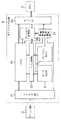
先ず、図1に、本発明の実施の形態に係るモデム装置としてのMODEM8を備えた通信端末装置としてのファクシミリ装置1のブロック構成を示す。
【0017】
同図において、ファクシミリ装置1は、ホスト側制御手段としてのCPU2、RAM3、プログラムROM4、I/O制御部5、スキャナ6、プロッタ7、MODEM8、網制御部11、省電力時回線状態監視部、切換回路13、操作表示部14及びシステムバス15により構成されている。
【0018】
システムバス15は、CPU2と、RAM3、プログラムROM4、I/O制御部5とがデータをやりとりする際の信号ラインである。
【0019】
CPU2は、プログラムROM4に書き込まれた制御プログラムに従って、RAM3を作業領域として使用しながら、装置各部を制御するマイクロコンピュータであり、MODEM8にとってのホスト側制御手段としての制御も行う。
【0020】
RAM3は、前述したようにCPU2の作業領域として使用されるランダムアクセスメモリである。プログラムROM4は、前述したように、システム制御部2が上記装置各部を制御するための制御プログラムやデータが記憶されているリードオンリメモリである。
【0021】
I/O制御部5は、システムバス15を介して接続されるCPU2と、I/O制御部5側に接続される各部とのデータのやりとりを制御するためのインターフェースである。
【0022】
スキャナ6は、原稿画像を読み取って画像データを得るためのものである。プロッタ7は、受信した画像データを、記録出力したり、スキャナ6で読み取った画像データを、その線密度に応じて記録出力するためのものである。
【0023】
MODEM8は、網制御部11及び切換回路13を介して電話回線に送信するデジタルデータをアナログ信号に変調したり、電話回線から受信するアナログ信号をデジタルデータに復調するためのものであり、アナログ信号のA/D、D/A変換のインターフェースとなるモデムアナログ部10と、変調や復調、呼び出し信号等の各種トーン信号の検出等の信号処理を行うモデムデジタル部9とにより構成されている。
【0024】
網制御部11は、電話回線に接続されて、回線の直流ループの閉結・解放や、回線の極性反転の検出、回線解放の検出、発信音の検出、ビジートーン等のトーン信号の検出、呼出信号の検出等の回線との接続制御や、ダイヤル番号に対応したダイヤルパルスの生成を行うものである。
【0025】
省電力時回線状態監視部13は、MODEM8が後述する省電力状態である場合に、MODEM8に代わって、呼び出し信号の有無等の回線状態を監視するためのものである。
【0026】
切換回路13は、I/O制御部5を介したCPU2からの指示に応じて、網制御部11を介した電話回線からの信号を、通常の動作状態時にはMODEM8側に接続するためのものである。
【0027】
操作表示部9は、相手先ファクシミリ番号を指定するためのテンキー、送信スタートキー、ワンタッチダイヤルキー、及び、その他各種キーが配設される一方、液晶表示装置等の表示器を備え、ユーザに知らせるべき装置の動作状態や、各種メッセージを表示するものである。
【0028】
図2に、MODEM8のモデムデジタル部9の第1実施形態に係るブロック構成を示す。
【0029】
同図において、ホストI/F22は、I/O制御部5とシステムバス15を介した、CPU2と、モデムデジタル部9内のDSP20、ダウンロード制御部26、及び、電源供給/起動制御部27との間のデータ交換を中継するインターフェースである。
【0030】
DSP20は、アナログ部I/F21を介してアナログ部10とやりとりされる各種信号についての演算処理を行うデジタル・シグナル・プロセッサであり、バス切替部23を介してプログラムRAM25にアクセスして処理手順を読み出し、データRAM24を作業領域として使用して各種信号処理を行う。
【0031】
バス切替部23は、ダウンロード制御部26からの制御により、プログラムラム25のデータ・アドレスバスを、通常の動作状態では、DSP20側に接続し、ダウンロード制御部26がホスト側のCPU2から転送されてくるプログラムデータをプログラムRAM25にダウンロードする際には、ダウンロード制御部26側に接続するものであり、また、プログラムRAM25のバスの切り離しも行う。
【0032】
電源供給/起動制御部27は、モデムデジタル部9内の比較的電力消費の多い構成、つまり、DSP20に加え、データRAM24、プログラムRAM25、アナログ部I/F21への電力供給を行うと共に、その電力供給の起動/停止を制御する。
【0033】
モデムデジタル部8は、その処理すべき信号処理プログラムをホスト側のCPU2からホストI/F22を経由してモデムデジタル部8のプログラムRAM25に格納して実行する。
【0034】
モデムデジタル部8の処理内容は、ホストからダウンロードされるモデムプログラム用コードによって決まり、ファクシミリ全体を制御するホスト側のCPU2がこれを決定している。
【0035】
ファクシミリ全体を制御するCPU2は、ホストI/F22を通してモデムに処理させるべきプログラムをプログラムROM4中に格納されたモデム用プログラムコードを選択してモデムにダウンロードする。
【0036】
CPU2は、通常動作時は、MODEM8に対して、プログラムROM4から処理の必要に応じたプログラムコードをダウンロードする。例えば、着呼直後には各種のトーン検出機能をダウンロードし、またファクシミリプロトコルが成立した後は、変調モードに応じた変復調用の処理プログラムコードをダウンロードする。
【0037】
本実施の形態では、ファクシミリ装置1が電源ONにより動作を開始してから省電力状態に移行し、その省電力状態から、着呼を復帰要因として通常の動作状態に復帰する場合についてその動作を説明する。
【0038】
ここで、ファクシミリ装置1本体側のCPU2、及び、MODEM8のモデムデジタル部9のそれぞれにおける、第1実施形態に係る、電源ONから動作状態への移行処理手順について図3を参照して説明する。
【0039】
同図において、CPU2及びモデムデジタル部9はそれぞれ装置電源がONされると動作を開始する。モデムデジタル部9においては、電源供給/起動制御部27によるモデムデジタル部9各部への電力供給が開始される(処理201)。
【0040】
そして、CPU2は、モデムデジタル部9のダウンロード制御部26に対して、コールドスタートを指示し(処理101)、ダウンロード制御部26が起動される(処理202)。
【0041】
処理202により起動されたダウンロード制御部26は、バス切替部23に指示してプログラムRAM25のバスラインをダウンロード制御部26側に一時的に切り替える(処理203)。
【0042】
一方CPU2は、予めプログラムROMにデータとして記憶していた、DSP20が処理すべきプログラムデータのモデムデジタル部9への転送を(処理102)、転送が終了するまで行い(判断103のNoのループ)、転送が終了すると(判断103のYes)、ファクシミリ装置としての通常の動作を行う状態である動作状態に移行する。
【0043】
一方モデムデジタル部9のダウンロード制御部26は、処理102によりCPU2からホストI/F22を介して転送されてくるプログラムデータを受信し(処理204)、バス切り替えされているプログラムラム25に転送する処理を(処理205)、プログラムデータの受信・転送が終了するまで繰り返し行い(判断206のNoのループ)、プログラムデータの受信・転送が終了すると(判断206のYes)、処理203により、ダウンロード制御部26側に一時的に切り替えられていたプログラムラム25のバスラインを、バス切替部23に指示して、DSP20側に切り替える。
【0044】
そして、ダウンロード制御部26は、DSP20を起動して(処理208)、DSP20がプログラムRAM25に格納されたプログラムに従って、データRAM24を作業領域として使用しながら各種信号処理を行う動作状態に移行する。
【0045】
モデムデジタル部9のDSP20は、動作状態において、ファクシミリ通信中における変復調処理等の各種信号処理を行うが、高速処理が必要となるため、動作状態におけるDSP20の電力消費量は多い。
【0046】
そのため、図4に示すように、ホスト側のCPU2、及び、モデムデジタル部9のそれぞれにおいて、第1実施形態に係る、動作状態から省電力状態への移行処理手順が行われる。
【0047】
同図において、CPU2は、一定時間(例えば15分間)着信(MODEM8による呼び出し信号の検出)がない状態が続いたかを監視し(判断301のNoのループ)、一定時間着信がない状態が続いた場合には(判断301のYes)、モデムデジタル部8のダウンロード制御部26に対して、省電力状態への移行を指示する(処理302)。
【0048】
一方、モデムデジタル部9では、処理302に呼応して、ダウンロード制御部26が起動される(処理401)。
【0049】
処理401により起動されたダウンロード制御部26は、バス切替部23に指示してプログラムRAM25のバスラインをダウンロード制御部26側に一時的に切り替える(処理402)。
【0050】
一方CPU2は、予めプログラムROMにデータとして記憶していた、DSP40が起動時に必要な処理プログラムのデータのモデムデジタル部9への転送を(処理303)、転送が終了するまで行い(判断304のNoのループ)、転送が終了すると(判断304のYes)、モデムデジタル部9のダウンロード制御部26に対してDSP20への電源供給の停止を指示すると共に(処理305)、それまで、網制御部11を、MODEM9のモデムアナログ部10に接続していた切換回路13を制御して、網制御部11を省電力時回線状態監視部12に切り換えた上で(処理306)、少なくとも、モデムデジタル部9のDSP20への電力供給が停止される(DSP20での着信検出ができなくなる)、省電力状態に移行する。
【0051】
一方モデムデジタル部9のダウンロード制御部26は、処理303によりCPU2からホストI/F22を介して転送されてくる起動プログラムデータを受信し(処理403)、バス切り替えされているプログラムラム25に転送する処理を(処理404)、起動プログラムデータの受信・転送が終了するまで繰り返し行い(判断405のNoのループ)、プログラムデータの受信・転送が終了すると(判断405のYes)、DSP20への電源供給の停止の指示を待ち(判断406のNoのループ)、CPU2側の処理305に対応して判断406がYesとなると、プログラムラム25のバスラインを、バス切替部23に指示して、DSP40から切り離す(処理407)。
【0052】
そして、電源供給/起動制御部27に指示して、プログラムRAM25以外への電源供給を停止する(処理408)。これにより、DSP20には電源が供給されなくなる分電力消費を抑えることができる一方、プログラムRAM25に記憶されたプログラムデータはそのまま保持される省電力状態に移行する。
【0053】
このようにして省電力状態に移行したホスト側のCPU2と、モデムデジタル部9とは、図5に示す、第1実施形態に係る、省電力状態から動作状態への復帰処理手順を行う。
【0054】
同図において、CPU2は、省電力時回線状態監視部12により電話回線からの着信があるかを監視し(判断501のNoのループ)、着信があると(判断501のYes)、モデムデジタル部9に対して、ウォームスタートを指示して(処理502)、動作状態に復帰する。
【0055】
一方、モデムデジタル部9では、CPU2からのウォームスタートの指示があるかを監視し(判断601のNoのループ)、指示があると(判断601のYes)、電源供給/起動制御部27によりそれまで電力供給が停止されていた、DSP20、データRAM24、及び、アナログ部I/F21にも電源供給を再開してモデムデジタル部9の各部の動作を可能とし(処理602)、バス切替部23によりプログラムRAM25のバスラインをDSP20に切り替えた上で(処理603)、DSP20を起動して(処理604)、プログラムRAM25に格納された起動プログラムによりDSP20の動作を開始させ、アナログ部I/F21を介してやりとりされる信号の処理をDSP20により行う、動作状態に移行し、判断501で着信した通信を処理する。
【0056】
これにより、モデムデジタル部9のDSP20が省電力状態に移行して動作停止され、再度動作状態に復帰する場合に、プログラムRAM25へのプログラムのダウンロードが不要で素早い起動が可能となり、動作状態に移行後における着信した通信に関する各種信号処理を迅速に開始することができるようになる。
【0057】
図6に、MODEM8のモデムデジタル部9の第2実施形態に係るブロック構成を示す。
【0058】
同図に示す第2実施形態に係るモデムデジタル部9は、図2に示した第1実施形態に係るモデムデジタル部9と同一構成であるが、ダウンロード制御部26が、誤り検出制御部26aを備えている点のみが異なる。
【0059】
誤り検出制御部26aは、ホスト側のCPU2から転送されてくるプログラムデータを元に誤り検出符号を生成するもので、生成された誤り検出符号は、プログラムRAM上にダウンロードされたプログラムデータの末尾に付加される。
【0060】
以上の構成の第2実施形態に係るモデムデジタル部9を備えたファクシミリ装置1本体側のCPU2、及び、モデムデジタル部9のそれぞれにおいては、図3に示した、第1実施形態に係る、電源ONから動作状態への移行処理手順と同一手順により動作状態に移行する。
【0061】
モデムデジタル部9のDSP20は、動作状態において、ファクシミリ通信中における変復調処理等の各種信号処理を行うが、高速処理が必要となるため、動作状態におけるDSP20の電力消費量は多い。
【0062】
そのため、図7に示すように、ホスト側のCPU2、及び、モデムデジタル部9のそれぞれにおいて、第2実施形態に係る、動作状態から省電力状態への移行処理手順が行われる。
【0063】
同図において、CPU2は、一定時間(例えば15分間)着信(MODEM8による呼び出し信号の検出)がない状態が続いたかを監視し(判断701のNoのループ)、一定時間着信がない状態が続いた場合には(判断701のYes)、モデムデジタル部8のダウンロード制御部26に対して、省電力状態への移行を指示する(処理702)。
【0064】
一方、モデムデジタル部9では、処理702に呼応して、ダウンロード制御部26が起動される(処理801)。
【0065】
処理801により起動されたダウンロード制御部26は、バス切替部23に指示してプログラムRAM25のバスラインをダウンロード制御部26側に一時的に切り替える(処理802)。
【0066】
一方CPU2は、予めプログラムROMにデータとして記憶していた、DSP80が起動時に必要な処理プログラムのデータのモデムデジタル部9への転送を(処理703)、転送が終了するまで行い(判断704のNoのループ)、転送が終了すると(判断704のYes)、モデムデジタル部9のダウンロード制御部26に対してDSP20への電源供給の停止を指示すると共に(処理705)、それまで、網制御部11を、MODEM9のモデムアナログ部10に接続していた切換回路13を制御して、網制御部11を省電力時回線状態監視部12に切り換えた上で(処理706)、少なくとも、モデムデジタル部9のDSP20への電力供給が停止され、操作表示部14の表示部の照明の消灯等のその他の省電力処理が行われる、省電力状態に移行する。
【0067】
一方モデムデジタル部9のダウンロード制御部26は、処理703によりCPU2からホストI/F22を介して転送されてくる起動プログラムデータを受信し、その転送されてきたプログラムデータについて誤り検出制御部26aにより誤り検出符号を生成する処理を行うと共に(処理803)、バス切り替えされているプログラムラム25に、受信したプログラムデータを転送する処理を(処理804)、起動プログラムデータの受信・転送が終了するまで繰り返し行い(判断805のNoのループ)、プログラムデータの受信・誤り検出符号の生成・転送が終了すると(判断805のYes)、処理803で生成した誤り検出符号をプログラムRAM25に格納した起動プログラムデータの末尾に付加する。
【0068】
そして、DSP20への電源供給の停止の指示を待ち(判断807のNoのループ)、CPU2側の処理705に対応して判断807がYesとなると、プログラムRAM25のバスラインを、バス切替部23に指示して、DSP80から切り離す(処理807)。
【0069】
そして、電源供給/起動制御部27に指示して、プログラムRAM25以外への電源供給を停止する(処理808)。これにより、DSP20には電源が供給されなくなる分電力消費を抑えることができる一方、プログラムRAM25に記憶されたプログラムデータはそのまま保持される省電力状態に移行する。
【0070】
このようにして省電力状態に移行したホスト側のCPU2と、モデムデジタル部9とは、図8及び図9に示す、第2実施形態に係る、省電力状態から動作状態への復帰処理手順を行う。
【0071】
先ず、図8において、CPU2は、省電力時回線状態監視部12により電話回線からの着信があるかを監視し(判断901のNoのループ)、着信があると(判断901のYes)、モデムデジタル部9に対して、ウォームスタートを指示して(処理902)、切換回路13をモデムアナログ部10側に切り換えた上で(処理903)、動作状態に移行し、判断901で着信した通信を処理する。
【0072】
一方、モデムデジタル部9では、CPU2からのウォームスタートの指示があるかを監視し(判断1001のNoのループ)、指示があると(判断1001のYes)、電源供給/起動制御部27によりそれまで電力供給が停止されていた、DSP20、データRAM24、及び、アナログ部I/F21にも電源供給を再開してモデムデジタル部9の各部の動作を可能とし(処理1002)、ダウンロード制御部26を起動し(処理1003)、バス切替部23によりプログラムRAM25のバスラインをダウンロード制御部26側の切り替え(処理1004)、プログラムRAM25の格納されている起動プログラムデータについて、誤り検出制御部26aより誤り検出符号を検出し(処理1005)、処理806によりプログラムRAM25の格納されている起動プログラムデータに付加していた誤り検出符号と比較する(処理1006)。
【0073】
そして、一致した場合には(判断1007のYes)、バス切替部23によりプログラムRAM25のバスラインをDSP20に切り替えた上で(処理1008)、DSP20を起動して(処理1009)、プログラムRAM25に格納された起動プログラムによりDSP20の動作を開始させ、アナログ部I/F21を介してやりとりされる信号の処理をDSP20により行う、動作状態に移行し、判断901で着信した通信を処理する。
【0074】
これにより、起動プログラムデータの内容に誤りがない場合には、モデムデジタル部9のDSP20が省電力状態に移行して動作停止され、再度動作状態に復帰する場合に、プログラムRAM25へのプログラムのダウンロードが不要で素早い起動が可能となり、動作状態に移行後における着信した通信に関する各種信号処理を迅速に開始することができるようになる。
【0075】
一方、判断1007において、誤り検出符号が一致しなかった場合には(判断1007のNo)、図9の処理1201に移行し、ホスト側のCPU2に対して、コールドスタートの要求を行う(処理1201)。
【0076】
一方、動作状態移行後のホスト側のCPU2は、モデムデジタル部9からのコールドスタートの要求があるかを監視し(判断1101のNoのループ)、コールドスタートの要求があると(判断1101のYes)、CPU2は、モデムデジタル部9のダウンロード制御部26に対して、コールドスタートを指示し(処理1102)、その指示に対して、ダウンロード制御部26は、バス切替部23に指示してプログラムRAM25のバスラインをダウンロード制御部26側に切り替える(処理1202)。
【0077】
一方CPU2は、予めプログラムROMにデータとして記憶していた、DSP20が処理すべきプログラムデータのモデムデジタル部9への転送を(処理1103)、転送が終了するまで行い(判断1104のNoのループ)、転送が終了すると(判断1104のYes)、動作状態に移行する。
【0078】
一方モデムデジタル部9のダウンロード制御部26は、処理1103によりCPU2からホストI/F22を介して転送されてくるプログラムデータを受信し(処理1203)、バス切り替えされているプログラムRAM25に転送する処理を(処理1204)、プログラムデータの受信・転送が終了するまで繰り返し行い(判断1205のNoのループ)、プログラムデータの受信・転送が終了すると(判断1205のYes)、ダウンロード制御部26側に一時的に切り替えられていたプログラムRAM25のバスラインを、バス切替部23に指示して、DSP20側に切り替える(処理1206)。
【0079】
そして、ダウンロード制御部26は、DSP20を起動して(処理1207)、DSP20がプログラムRAM25に格納されたプログラムに従って、データRAM24を作業領域として使用しながら各種信号処理を行う動作状態に移行する。
【0080】
これにより、起動プログラムデータの内容に誤りがある場合には、モデムデジタル部9のDSP20が省電力状態に移行して動作停止され、再度動作状態に復帰する場合に、予期せぬ電源変動等により破損したプログラムデータによりMODEM8が起動することを防止でき、動作の信頼性を損なうことなくMODEM8の起動時間を短縮することができる。
【0081】
なお、以上説明した実施の形態においては、通信端末装置の1つである、MOモデム装置によりファクシミリメッセージをやりとりするファクシミリ装置に本発明を適用したが、本発明はモデムによりやりとりされるデータの内容により限定されるものではなく、プログラムRAMに格納されたプログラムデータに基づいて動作するDSPにより構成されたモデム装置を備えた通信端末装置であれば、同様に適用可能なものである。
【0082】
【発明の効果】
請求項1に係る発明によれば、前記DSPが動作するためのプログラムがRAMに記憶される場合でも、前記プログラムRAMが前記DSPとは独立した電源供給によりプログラムデータを保持することができ、また、保持されたプログラムデータにより前記DSPを起動することができるため、起動の際のプログラムダウンロード時間が不要となり、本発明に係るモデム装置の起動時間を短縮することが可能となる効果が得られる。
【0083】
請求項2に係る発明によれば、前記DSPを前記プログラムRAMに保持されたプログラムデータから起動するウォームスタート時に、予期せぬ電源変動等により前記プログラムRAMに保持されたプログラムデータが破損した状態で前記DSPが起動してしまう事を回避でき、動作の信頼性を損わずに、本発明に係るモデム装置の起動時間を短縮することが可能となる効果が得られる。
【0084】
請求項3に係る発明によれば、前記モデム装置として、請求項1または2のいずれかに記載のモデム装置を適用することにより、前記DSPへの電源供給が停止される前記省電力状態から前記通常常態に復帰時の起動時間を短縮できるため、消費電力の抑制と起動時間の短縮とを両立した通信端末装置を実現することが可能となる効果が得られる。
【図面の簡単な説明】
【図1】本発明の実施の形態に係るモデム装置(MODEM)を備えた通信端末装置としてのファクシミリ装置のブロック構成を示す図である。
【図2】本発明の実施の形態に係るモデム装置(MODEM)の第1実施形態に係るモデムデジタル部のブロック構成について示す図である。
【図3】ファクシミリ装置本体側のCPU及びモデム装置(MODEM)のモデムデジタル部のそれぞれにおける、第1実施形態に係る、電源ONから動作状態への移行処理手順について示すフローチャートである。
【図4】ファクシミリ装置本体側のCPU及びモデム装置(MODEM)のモデムデジタル部のそれぞれにおける、第1実施形態に係る、動作状態から省電力状態への移行処理手順について示すフローチャートである。
【図5】ファクシミリ装置本体側のCPU及びモデム装置(MODEM)のモデムデジタル部のそれぞれにおける、第1実施形態に係る、省電力状態から動作状態への復帰処理手順について示すフローチャートである。
【図6】本発明の実施の形態に係るモデム装置(MODEM)の、第2実施の形態に係るモデムデジタル部のブロック構成について示す図である。
【図7】ファクシミリ装置本体側のCPU及びモデム装置(MODEM)のモデムデジタル部のそれぞれにおける、第2実施形態に係る、動作状態から省電力状態への移行処理手順について示すフローチャートである。
【図8】ファクシミリ装置本体側のCPU及びモデム装置(MODEM)のモデムデジタル部のそれぞれにおける、第2実施形態に係る、省電力状態から動作状態への復帰処理手順について示すフローチャートである。
【図9】図8と共に、ファクシミリ装置本体側のCPU及びモデム装置(MODEM)のモデムデジタル部のそれぞれにおける、第2実施形態に係る、省電力状態から動作状態への復帰処理手順について示すフローチャートである。
【符号の説明】
1 ファクシミリ装置
2 CPU
3 RAM
4 プログラムROM
5 I/O制御部
6 スキャナ
7 プロッタ
8 MODEM(モデム装置)
9 モデムデジタル部
10 モデムアナログ部
11 網制御部
12 省電力時回線状態監視部
13 切換回路
14 操作表示部
20 DSP
21 アナログI/F部
22 ホストI/F
23 バス切換部
24 データRAM
25 プログラムRAM
26 ダウンロード制御部
26a 誤り検出制御部
27 電源供給/起動制御部[0001]
BACKGROUND OF THE INVENTION
The present invention relates to a modem device and a communication terminal device including the modem device, and more particularly, a program RAM in which program data is stored and an analog such as a telephone line that operates based on the program data stored in the program RAM. The present invention relates to a modem device including at least a DSP (digital signal processor) that processes communication signals exchanged via a line, and a communication terminal device including the modem device.
[0002]
[Prior art]
In communication terminal devices such as facsimile machines, it is strongly required to reduce power consumption in consideration of the environment.
[0003]
Therefore, in the standby state where there is no transmission operation by the operator and only waiting for an incoming call from the line, unnecessary power consumption is suppressed by suppressing circuit operations other than the operator operation and the function for monitoring the incoming call from the line. Things have been done.
[0004]
On the other hand, in a modem device that is indispensable when a communication terminal device such as a facsimile device performs communication via an analog line such as a telephone line, an A / D converter or D / A conversion is performed on an analog communication signal exchanged. A DSP (digital signal processor) that performs high-speed signal processing at a digital signal level through a device is used.
[0005]
However, the DSP is required to have a high processing capacity for high-speed signal processing, and the power consumption is not small.
[0006]
Therefore, in communication terminal devices such as conventional facsimile devices, in order to reduce power consumption of the modem, power is not supplied to the modem or the modem is shifted to a low power consumption operation. The power consumption is reduced.
[0007]
On the other hand, with recent enhancement of functions of facsimile modems and data modems, a large-capacity memory is required as a memory for storing programs necessary for the operation of the DSP constituting the modem device.
[0008]
Conventionally, ROM (read only memory) has been used as a program memory for DSP. However, in order to construct a modem using DSP at a lower cost, the host side (external to the modem ( A device having a program RAM (random access memory) for downloading a program from a communication terminal device CPU or the like on which a modem is mounted is used.
[0009]
[Problems to be solved by the invention]
However, since the program RAM does not retain its value when the power is off, an incoming call from the line is detected in the power saving state in which the power supply to the modem configuration including the program RAM and DSP is stopped in the power saving state. Thus, when returning to the normal operation state, it is necessary to re-download the program for the DSP operation into the program RAM.
[0010]
On the other hand, when an incoming call from the line is detected in the power saving state and the normal operation state is restored, the DSP may need to start signal processing promptly. If the download to the RAM is performed every time the power saving state is restored to the normal operation state, the start of the signal processing in the DSP is delayed, which hinders the modem signal processing after the return to the normal operation state. There was a problem that it might end.
[0011]
The present invention has been made in view of such circumstances, and a modem device capable of quick restart without needing to download a program to a DSP program RAM when returning from a power saving state to a normal operation state. An object of the present invention is to provide a communication terminal device provided with the modem device.
[0012]
[Means for Solving the Problems]
The modem device according to claim 1 operates based on a program RAM in which program data is stored and the program data stored in the program RAM. A In a modem apparatus including at least a DSP (digital signal processor) that processes communication signals exchanged via a analog line, the program RAM is supplied with power through a system different from the DSP and supplies power to the DSP. The stored contents are retained even when the DSP is stopped, and when the DSP is started, the external host side control means is requested to download new program data to the program RAM, and the request is made in response to the request. The new program data transferred from the host-side control means is received and stored in the program RAM and then the DSP is started, and the program data held in the program RAM is used as it is. Warm start mode to start DSP and Characterized by comprising a control means for activating the DSP in one of start-up mode.
[0013]
The modem device according to
[0014]
The communication terminal device according to claim 3 A A communication terminal device for performing communication by processing a communication signal exchanged via a analog line by a modem device, comprising the modem device according to
[0015]
DETAILED DESCRIPTION OF THE INVENTION
Hereinafter, embodiments of the present invention will be described in detail with reference to the accompanying drawings.
[0016]
First, FIG. 1 shows a block configuration of a facsimile apparatus 1 as a communication terminal apparatus provided with a MODEM 8 as a modem apparatus according to an embodiment of the present invention.
[0017]
In the figure, a facsimile apparatus 1 includes a
[0018]
The
[0019]
The
[0020]
The
[0021]
The I / O control unit 5 is an interface for controlling data exchange between the
[0022]
The
[0023]
The MODEM 8 is used to modulate digital data transmitted to the telephone line via the
[0024]
The
[0025]
The power-saving line
[0026]
The switching
[0027]
The
[0028]
FIG. 2 shows a block configuration according to the first embodiment of the modem
[0029]
In the figure, the host I /
[0030]
The
[0031]
Under the control of the
[0032]
The power supply / start-up
[0033]
The modem digital unit 8 stores the signal processing program to be processed from the
[0034]
The processing contents of the modem digital unit 8 are determined by the code for the modem program downloaded from the host, and this is determined by the
[0035]
The
[0036]
During normal operation, the
[0037]
In the present embodiment, when the facsimile apparatus 1 starts operating when the power is turned on, the facsimile apparatus 1 shifts to the power saving state, and when the incoming call is returned to the normal operating state as a return factor from the power saving state, the operation is performed. explain.
[0038]
Here, the transition processing procedure from the power ON to the operation state according to the first embodiment in each of the
[0039]
In the figure, the
[0040]
Then, the
[0041]
The
[0042]
On the other hand, the
[0043]
On the other hand, the
[0044]
Then, the
[0045]
The
[0046]
Therefore, as shown in FIG. 4, the transition processing procedure from the operation state to the power saving state according to the first embodiment is performed in each of the
[0047]
In the figure, the
[0048]
On the other hand, in the modem
[0049]
The
[0050]
On the other hand, the
[0051]
On the other hand, the
[0052]
Then, the power supply /
[0053]
The host-
[0054]
In the figure, the
[0055]
On the other hand, the modem
[0056]
As a result, when the
[0057]
FIG. 6 shows a block configuration according to the second embodiment of the modem
[0058]
The modem
[0059]
The error detection control unit 26a generates an error detection code based on the program data transferred from the
[0060]
In each of the
[0061]
The
[0062]
Therefore, as shown in FIG. 7, the transition processing procedure from the operation state to the power saving state according to the second embodiment is performed in each of the
[0063]
In the figure, the
[0064]
On the other hand, in the modem
[0065]
The
[0066]
On the other hand, the
[0067]
On the other hand, the
[0068]
Then, it waits for an instruction to stop the power supply to the DSP 20 (No loop in the determination 807). When the
[0069]
Then, the power supply /
[0070]
The host-
[0071]
First, in FIG. 8, the
[0072]
On the other hand, the modem
[0073]
If they match (Yes in decision 1007), the
[0074]
As a result, when there is no error in the contents of the startup program data, the
[0075]
On the other hand, if the error detection codes do not match in the decision 1007 (No in the decision 1007), the processing shifts to the processing 1201 in FIG. 9, and a cold start request is made to the
[0076]
On the other hand, the
[0077]
On the other hand, the
[0078]
On the other hand, the
[0079]
Then, the
[0080]
As a result, when there is an error in the contents of the startup program data, the
[0081]
In the embodiment described above, the present invention is applied to a facsimile apparatus that exchanges a facsimile message by an MO modem apparatus, which is one of communication terminal apparatuses. However, the present invention is a content of data exchanged by a modem. However, the present invention is similarly applicable to any communication terminal device including a modem device configured by a DSP that operates based on program data stored in the program RAM.
[0082]
【The invention's effect】
According to the first aspect of the present invention, even when a program for operating the DSP is stored in the RAM, the program RAM can hold program data by power supply independent of the DSP, and Since the DSP can be activated by the stored program data, the program download time at the time of activation is not required, and the activation time of the modem device according to the present invention can be shortened.
[0083]
According to the second aspect of the present invention, in a warm start in which the DSP is started from the program data held in the program RAM, the program data held in the program RAM is damaged due to an unexpected power supply fluctuation or the like. The DSP can be prevented from being activated, and the activation time of the modem device according to the present invention can be shortened without impairing operational reliability.
[0084]
According to the invention according to
[Brief description of the drawings]
FIG. 1 is a diagram showing a block configuration of a facsimile apparatus as a communication terminal apparatus provided with a modem apparatus (MODEM) according to an embodiment of the present invention.
FIG. 2 is a diagram showing a block configuration of a modem digital unit according to the first embodiment of the modem device (MODEM) according to the embodiment of the present invention;
FIG. 3 is a flowchart showing a transition processing procedure from the power-on to the operating state according to the first embodiment in each of the CPU on the facsimile apparatus main body and the modem digital unit of the modem apparatus (MODEM).
FIG. 4 is a flowchart illustrating a transition processing procedure from an operation state to a power saving state according to the first embodiment in each of the CPU on the facsimile apparatus main body and the modem digital unit of the modem apparatus (MODEM).
FIG. 5 is a flowchart showing a procedure for returning from the power saving state to the operating state according to the first embodiment in each of the CPU on the main body side of the facsimile apparatus and the modem digital unit of the modem apparatus (MODEM).
FIG. 6 is a diagram showing a block configuration of a modem digital unit according to a second embodiment of the modem device (MODEM) according to the embodiment of the present invention.
FIG. 7 is a flowchart illustrating a transition processing procedure from an operation state to a power saving state according to the second embodiment in each of the CPU on the facsimile apparatus main body and the modem digital unit of the modem apparatus (MODEM).
FIG. 8 is a flowchart illustrating a procedure for returning from a power saving state to an operating state according to the second embodiment in each of the CPU on the facsimile apparatus main body and the modem digital unit of the modem apparatus (MODEM).
FIG. 9 is a flowchart showing a procedure for returning from the power saving state to the operating state according to the second embodiment in each of the CPU on the main body side of the facsimile apparatus and the modem digital unit of the modem apparatus (MODEM) together with FIG. 8; is there.
[Explanation of symbols]
1 Facsimile device
2 CPU
3 RAM
4 Program ROM
5 I / O control unit
6 Scanner
7 Plotter
8 MODEM (modem equipment)
9 Modem digital part
10 Modem analog part
11 Network control unit
12 Power-saving line status monitoring unit
13 Switching circuit
14 Operation display
20 DSP
21 Analog I / F section
22 Host I / F
23 Bus switching part
24 data RAM
25 Program RAM
26 Download controller
26a Error detection control unit
27 Power supply / startup control unit
Claims (3)
前記プログラムRAMは、前記DSPとは異なる系統で電源供給されて前記DSPへの電源供給が停止さている状態でもその記憶内容を保持する一方、前記DSPの起動時に、外部のホスト側制御手段に対して前記プログラムRAMへの新しいプログラムデータのダウンロードを要求してその要求に呼応して前記ホスト側制御手段から転送される当該新しいプログラムデータを受信して前記プログラムRAMに格納した上で前記DSPを起動するコールドスタートのモードと、前記プログラムRAMに保持されたプログラムデータをそのまま使用して前記DSPを起動するウォームスタートのモードとのいずれかの起動モードで前記DSPを起動する制御手段を備えたことを特徴とするモデム装置。A program RAM in which the program data is stored, its operates based on programs stored data in the program RAM, comprising at least a DSP (digital signal processor) for processing communication signals exchanged via the analog line In a modem device,
The program RAM retains its stored contents even when power is supplied from a system different from the DSP and power supply to the DSP is stopped. On the other hand, when the DSP is started up, Requesting the download of new program data to the program RAM, receiving the new program data transferred from the host side control means in response to the request, storing the program data in the program RAM, and starting the DSP Control means for starting up the DSP in any one of the start mode of the cold start mode and the warm start mode of starting the DSP using the program data held in the program RAM as it is. A characteristic modem device.
前記モデム装置として、請求項1または2のいずれかに記載のモデム装置を備え、通常の動作状態から少なくとも前記DSPへの電源供給が停止される省電力状態に移行する際には、当該省電力状態から動作状態に復帰後最初に必要なモデム動作処理のプログラムを前記モデム装置側のプログラム用RAMにダウンロードし、前記省電力状態から動作状態に復帰する際には、前記モデム装置側の前記制御手段にウォームスタートを指示して、ウォームスタートのモードで前記DSPを起動させるホスト側制御手段を備えたことを特徴とする通信端末装置。A communication terminal apparatus that performs communication processing by the modem device communication signals exchanged via the analog line,
The modem device according to claim 1 or 2 as the modem device, and when shifting from a normal operation state to a power saving state where power supply to at least the DSP is stopped, After returning from the state to the operation state, the first necessary modem operation processing program is downloaded to the program RAM on the modem device side, and when returning from the power saving state to the operation state, the control on the modem device side is performed. A communication terminal apparatus comprising host-side control means for instructing the means to start a warm start and starting the DSP in a warm start mode.
Priority Applications (1)
| Application Number | Priority Date | Filing Date | Title |
|---|---|---|---|
| JP2000385356A JP3845258B2 (en) | 2000-12-19 | 2000-12-19 | MODEM DEVICE AND COMMUNICATION TERMINAL DEVICE |
Applications Claiming Priority (1)
| Application Number | Priority Date | Filing Date | Title |
|---|---|---|---|
| JP2000385356A JP3845258B2 (en) | 2000-12-19 | 2000-12-19 | MODEM DEVICE AND COMMUNICATION TERMINAL DEVICE |
Publications (3)
| Publication Number | Publication Date |
|---|---|
| JP2002185549A JP2002185549A (en) | 2002-06-28 |
| JP2002185549A5 JP2002185549A5 (en) | 2006-02-23 |
| JP3845258B2 true JP3845258B2 (en) | 2006-11-15 |
Family
ID=18852634
Family Applications (1)
| Application Number | Title | Priority Date | Filing Date |
|---|---|---|---|
| JP2000385356A Expired - Fee Related JP3845258B2 (en) | 2000-12-19 | 2000-12-19 | MODEM DEVICE AND COMMUNICATION TERMINAL DEVICE |
Country Status (1)
| Country | Link |
|---|---|
| JP (1) | JP3845258B2 (en) |
Cited By (1)
| Publication number | Priority date | Publication date | Assignee | Title |
|---|---|---|---|---|
| CN109922014A (en) * | 2019-02-01 | 2019-06-21 | 南京国电南自软件工程有限公司 | A kind of cold and hot starting judgment method of interchanger and system |
Families Citing this family (11)
| Publication number | Priority date | Publication date | Assignee | Title |
|---|---|---|---|---|
| US8284323B2 (en) | 2007-07-18 | 2012-10-09 | Panasonic Corporation | Video audio processing device and standby and return method thereof |
| JP4881901B2 (en) * | 2008-03-17 | 2012-02-22 | シャープ株式会社 | Image forming system |
| JP5278221B2 (en) * | 2009-07-21 | 2013-09-04 | 富士ゼロックス株式会社 | Information processing apparatus, image processing system, and program |
| JP2011061309A (en) * | 2009-09-07 | 2011-03-24 | Ricoh Co Ltd | Image processing apparatus |
| CN102263874B (en) | 2010-05-28 | 2014-03-12 | 京瓷办公信息系统株式会社 | Image forming apparatus having power saving mode |
| JP5910408B2 (en) * | 2012-08-09 | 2016-04-27 | ブラザー工業株式会社 | Communication device |
| JP2014112819A (en) | 2012-10-30 | 2014-06-19 | Yokogawa Electric Corp | Radio equipment, input/output unit, radio unit and radio equipment setup method |
| JP5898642B2 (en) | 2013-05-20 | 2016-04-06 | 横河電機株式会社 | Wireless equipment |
| JP6589681B2 (en) * | 2016-02-19 | 2019-10-16 | コニカミノルタ株式会社 | Image forming apparatus, activation control method, and activation control program |
| WO2017088531A1 (en) * | 2016-03-28 | 2017-06-01 | 中车青岛四方车辆研究所有限公司 | Tigersharc series dsp start-up management chip and method |
| CN111722878A (en) * | 2020-06-19 | 2020-09-29 | 北京集创北方科技股份有限公司 | Chip starting control method, chip, display panel and electronic equipment |
-
2000
- 2000-12-19 JP JP2000385356A patent/JP3845258B2/en not_active Expired - Fee Related
Cited By (2)
| Publication number | Priority date | Publication date | Assignee | Title |
|---|---|---|---|---|
| CN109922014A (en) * | 2019-02-01 | 2019-06-21 | 南京国电南自软件工程有限公司 | A kind of cold and hot starting judgment method of interchanger and system |
| CN109922014B (en) * | 2019-02-01 | 2020-12-29 | 南京国电南自软件工程有限公司 | Method and system for judging cold and hot start of switch |
Also Published As
| Publication number | Publication date |
|---|---|
| JP2002185549A (en) | 2002-06-28 |
Similar Documents
| Publication | Publication Date | Title |
|---|---|---|
| JP3845258B2 (en) | MODEM DEVICE AND COMMUNICATION TERMINAL DEVICE | |
| JP4522347B2 (en) | Facsimile MFP | |
| JP2002344673A (en) | Image forming system | |
| JP2002218099A (en) | Communication system | |
| JP2002359703A (en) | Image forming device | |
| JPH11168559A (en) | Call controller and exchange system using the call controller | |
| JP5796374B2 (en) | Image processing apparatus, image processing method, and program | |
| JP2001061027A (en) | Electric apparatus and communication terminal | |
| JPH10173832A (en) | Facsimile equipment | |
| JP2004135215A (en) | Electronic apparatus and remote control system for the electronic apparatus | |
| JPH0969889A (en) | Data processor | |
| JP3851479B2 (en) | Image forming apparatus | |
| JPH11289419A (en) | Combined device | |
| JP3136936B2 (en) | Facsimile machine with energy saving function | |
| JP3480783B2 (en) | Compound facsimile machine | |
| US5956155A (en) | Facsimile apparatus having a modem function | |
| US7224688B2 (en) | Communication terminal device and method for controlling same | |
| JPH11161381A (en) | Power mode informing device, power mode notifying device, and storage medium for program used by the notifying device | |
| JP3370818B2 (en) | Facsimile machine | |
| JPH11243464A (en) | Facsimile equipment | |
| JP3576839B2 (en) | Communication terminal device and communication terminal control method | |
| JPH0983669A (en) | Modem equipment | |
| JP2006217647A (en) | Data communication apparatus | |
| JPH04209056A (en) | Personal computer with communication function | |
| JP2774867B2 (en) | Communication device and control method thereof |
Legal Events
| Date | Code | Title | Description |
|---|---|---|---|
| A621 | Written request for application examination |
Free format text: JAPANESE INTERMEDIATE CODE: A621 Effective date: 20041108 |
|
| A521 | Written amendment |
Free format text: JAPANESE INTERMEDIATE CODE: A523 Effective date: 20060111 |
|
| A977 | Report on retrieval |
Free format text: JAPANESE INTERMEDIATE CODE: A971007 Effective date: 20060619 |
|
| TRDD | Decision of grant or rejection written | ||
| A01 | Written decision to grant a patent or to grant a registration (utility model) |
Free format text: JAPANESE INTERMEDIATE CODE: A01 Effective date: 20060815 |
|
| A61 | First payment of annual fees (during grant procedure) |
Free format text: JAPANESE INTERMEDIATE CODE: A61 Effective date: 20060818 |
|
| R150 | Certificate of patent or registration of utility model |
Free format text: JAPANESE INTERMEDIATE CODE: R150 |
|
| FPAY | Renewal fee payment (event date is renewal date of database) |
Free format text: PAYMENT UNTIL: 20090825 Year of fee payment: 3 |
|
| FPAY | Renewal fee payment (event date is renewal date of database) |
Free format text: PAYMENT UNTIL: 20100825 Year of fee payment: 4 |
|
| FPAY | Renewal fee payment (event date is renewal date of database) |
Free format text: PAYMENT UNTIL: 20100825 Year of fee payment: 4 |
|
| FPAY | Renewal fee payment (event date is renewal date of database) |
Free format text: PAYMENT UNTIL: 20110825 Year of fee payment: 5 |
|
| FPAY | Renewal fee payment (event date is renewal date of database) |
Free format text: PAYMENT UNTIL: 20110825 Year of fee payment: 5 |
|
| FPAY | Renewal fee payment (event date is renewal date of database) |
Free format text: PAYMENT UNTIL: 20120825 Year of fee payment: 6 |
|
| FPAY | Renewal fee payment (event date is renewal date of database) |
Free format text: PAYMENT UNTIL: 20120825 Year of fee payment: 6 |
|
| FPAY | Renewal fee payment (event date is renewal date of database) |
Free format text: PAYMENT UNTIL: 20130825 Year of fee payment: 7 |
|
| LAPS | Cancellation because of no payment of annual fees |