JP3843532B2 - Liquid crystal display - Google Patents
Liquid crystal display Download PDFInfo
- Publication number
- JP3843532B2 JP3843532B2 JP10004397A JP10004397A JP3843532B2 JP 3843532 B2 JP3843532 B2 JP 3843532B2 JP 10004397 A JP10004397 A JP 10004397A JP 10004397 A JP10004397 A JP 10004397A JP 3843532 B2 JP3843532 B2 JP 3843532B2
- Authority
- JP
- Japan
- Prior art keywords
- liquid crystal
- thin film
- film separator
- substrates
- pair
- Prior art date
- Legal status (The legal status is an assumption and is not a legal conclusion. Google has not performed a legal analysis and makes no representation as to the accuracy of the status listed.)
- Expired - Fee Related
Links
Images


Description
【0001】
【発明の属する技術分野】
2つの液晶層を有する2層積層型液晶表示装置に係り、特に、液晶層に2色性色素を含有するゲストホスト型の2層積層型カラー液晶表示装置の最適構造に関する。
【0002】
【従来の技術】
従来、一対の基板を二対利用した液晶表示装置があったが、これらは視差が生じていた。また、特に、2層直交積層型の液晶表示装置にカラーフィルタとを組み合わせて反射型カラー液晶表示装置において問題となっていた。視差とは、使用者が観察する光が液晶表示装置に入射し、反射板で反射され、液晶表示装置から出射して使用者に到達する過程で入射時とは異なった画素に入り込む現象であり、視差が生じると、コントラスト比や表示色の彩度が低下する。この視差を解消するために、特開平7−159805 号では液晶層の間に誘電体層を設け、液晶層を分割している。
【0003】
【発明が解決しようとする課題】
しかし、特開平7−159805 号の構成の液晶表示装置は、誘電体層と基板とをシール剤で接着する際に、基板間のギャップが所定のギャップにならず、光透過特性が変化するという問題があった。これは、薄膜セパレータを有さない液晶表示装置では通常一対の基板の間は液晶層と1層のスペーサビーズを挟持しているので、ギャップを制御できるが、薄膜セパレータを用いる液晶表示装置ではセパレータを介して2層のスペーサビーズを有し、基板と薄膜セパレータを接着する際に基板に圧力をかけると、それぞれの基板と薄膜セパレータとがスペーサビーズのみを介して保持されているため、図7の様に、薄膜セパレータに中心に対して線対称にスペーサビーズが形成されないところでは薄膜セパレータが非常に歪みやすく、基板間ギャップが均一でなくなるという問題があった。同様に、2層のスペーサビーズで挟持されていたので基板自体の強度が低下するとともに、基板と薄膜セパレータを接着する分だけ接着力が低下し、剥離を起こしやすかったために歩留まりが低下していた。
【0004】
本発明の目的は、セルギャップを保持することで光透過特性が一定で、セル強度が強い2層積層型液晶表示装置、特に2層直交積層型液晶表示装置を実現することにある。
【0005】
また、特開平7−159805 号の液晶層の間の誘電体層(以後、薄膜セパレータとする)はごく薄いため、ラビング等の機械的なストレスによる配向処理方法は用いることができないという問題がある。また、ラビングできるように厚い誘電体を用いることも可能だが、それでは誘電体を用いる利点が無くなってしまう。そこで、本発明のさらなる目的は、薄膜セパレータの歪まない液晶表示装置において、その薄膜セパレータとしてラビング以外の手法で液晶分子を様々な配向方向に配向させることができる薄膜セパレータを用いることにある。特に、2つの固有偏光の両方を充分に吸収でき、高コントラスト比,高輝度,高色純度が実現可能な2層直交積層型液晶表示装置を実現することにある。
【0006】
【課題を解決するための手段】
上記課題を解決する手段としては、一対の基板と、その一対の基板挟持された薄膜セパレータと、その一対の基板のそれぞれと前記薄膜セパレータに挟持された液晶層と、前記液晶層に形成され前記一対の基板と薄膜セパレータの間隔を保持する第1のスペーサビーズと、前記一対の基板の対向面端部に形成されたシール部と、前記シール部に形成され前記一対の基板を挟持する第2のスペーサビーズとを有する構成とする。
【0007】
上記構成に対して、さらに、第2のスペーサビーズの一対の基板に対する法線方向の長さは第1のスペーサビーズの一対の基板の法線方向の長さよりも長くした構成を加えてもよい。
【0008】
同様な効果を生じる液晶表示装置の構成としては、一対の基板と、その一対の基板挟持された薄膜セパレータと、その一対の基板のそれぞれと薄膜セパレータに挟持された液晶層と、その液晶層に形成され一対の基板と薄膜セパレータの間隔を保持する第1のスペーサビーズと、基板の対向面端部に形成されたシール部と、前記シール部に形成された第2のスペーサビーズを有し、薄膜セパレータは前記一対の基板の対向面よりも面積が小さく、シール部は薄膜セパレータの外側に形成される構成が考えられる。
【0009】
また、上記薄膜セパレータ近傍での液晶分子は前記薄膜セパレータに対して垂直に配向され、一対の基板のそれぞれの基板近傍での液晶分子はそれぞれの基板に対してほぼ平行に配向され、基板平面に対して法線方向から見て第1の基板と第2基板界面の液晶分子は互いに直交する様に配向処理されることが好ましい。
また、薄膜セパレータ近傍での液晶分子は薄膜セパレータに対して水平に配向され、第1の基板平面の法線方向から見て薄膜セパレータの両面での液晶配向方向は直交するように配向処理されることが好ましい。
【0010】
さらに、薄膜セパレータを垂直配向性の高分子フィルムである垂直配向膜を両面に塗布した透明薄膜にしてもよい。
【0011】
また、薄膜セパレータは延伸して成膜化された2枚の高分子フィルムの積層体であり、前記2枚の高分子フィルムの延伸方向が直交する様に積層されているものでもよい。
【0012】
【発明の実施の形態】
図2(e)に本発明の液晶表示装置の断面図を示す。薄膜セパレータ45は基板よりも面積が小さく、シール部70の内側に分布し、かつ表示部全体を覆う様に分布する。シール部には直径がシール部よりも内側に配置したスペーサビーズの直径よりも大きく、望ましくは2つの液晶層の厚みと薄膜セパレータの厚さの和に概略等しいスペーサビーズを混入する。2つの対向基板を薄膜セパレータを介さずにシール部で直接に保持されるため、液晶セルの強度は従来の単層の液晶セルと同程度にまで向上し、同様にセルギャップを均一にすることができる。また、接着面の数も従来の単層の液晶セルと同じであるため、剥離の発生も従来の単層の液晶セルと同程度に低い。
【0013】
次に、薄膜セパレータで隔てられた2層の液晶層の配向方向を直交させるための手段について述べる。
【0014】
延伸法により作成された高分子フィルムの多くは、その両面近傍における液晶分子を延伸方向に向けて水平に配向させる作用を有する。しかし、側鎖に長鎖アルキル基等のバルキリーな基を有する有機高分子からなる高分子フィルムには、垂直配向性を示すものも有る。
【0015】
薄膜セパレータを垂直配向性の高分子フィルムで形成する。また、2つの対向基板の液晶層と近接する側にはプレチルト角が45度以下となる水平配向性の配向膜を塗布する。これら2層の配向膜にラビング法により配向処理を施し、その配向処理方向は基板方線方向から見て直交する様に設定する。
【0016】
或いはまた、薄膜セパレータに水平配向性の高分子フィルムの両面に垂直配向性のポリイミド膜を塗布したものを用いても、これと同様の液晶配向が実現される。
【0017】
また、薄膜セパレータに水平配向性の高分子フィルムを2枚積層したものを用い、その2枚の高分子フィルムは、延伸方向が直交する様に積層する。対向基板の配向膜は垂直配向膜としても、水平配向膜としても良い。
【0018】
以上の方法により、薄膜セパレータで隔てられた2層の液晶層の配向方向を直交させることができる。
【0019】
本発明の実施の具体的な形態を以下に示す。
【0020】
「実施例1」
図1に本発明の液晶表示装置の液晶セルの構造を示す透視図を示す。
【0021】
一対の基板の一方(以下、第1の基板と称する)はホウケイサンガラス製であり、厚さは0.7mm であり、配向膜,共通電極,平坦化層,カラーフィルタが順次積層されている。配向膜はポリイミド系高分子であり、層厚は1000Åであり、ラビング法により配向処理され、そのプレチルト角は10°である。共通電極はITO製であり、層厚は1000Åである。平坦化層はエポキシ樹脂製であり、層厚は2μmである。カラーフィルタは染色法で作成し、透過率が最低になる波長での透過率はR,G,Bいずれのカラーフィルタでも約50%である。
【0022】
一対の基板の他方(以下、第2の基板と称する)は第1の基板と同じ材質と厚さであり、配向膜,反射電極,絶縁層,アクティブ素子が順次積層されている。配向膜は第1の基板上のものと同様である。反射電極はAl製であり、層厚は2000Åである。絶縁層はSINx製であり、層厚は1μmである。アクティブ素子は逆スタガ型の薄膜トランジスタである。反射電極は1画素を形成し、その形状は概略長方形状であり、大きさは約100μm×900μmである。反射電極とアクティブ素子はスルーホールにより接続されている。
【0023】
薄膜セパレータはポリイミド系高分子の薄膜であり、膜厚は2μmである。薄膜セパレータのポリイミド系高分子には、側鎖に長鎖アルキル基を有するものを用いた。薄膜セパレータ表面は側鎖の長鎖アルキル基によって覆われ、長鎖アルキル基は配向膜平面法線方向に向かって伸びていると考えられる。液晶分子は長鎖アルキル基に沿う様に配向し、結果として垂直配向となると考えられる。
【0024】
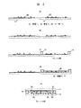
その後の第1の基板、第2の基板に対する処理と組立てを図2に示す。第1の基板、第2の基板の各層が積層されている側に直径5μmの固着型ビーズを1cm2 あたり200個の密度で分散した(図2(a))。その後、基板を加熱し、固着型ビーズを基板上に固定した(図2(b))。次に、シール剤を第1の基板上に印刷し、シール部とした(図2(c))。シール剤中には、直径が13μmのビーズを混合した。シール剤中のビーズの直径は、第1の液晶層、第2の液晶層(各5μm、固着ビーズの基板に法線方向の等しいとする)と、薄膜セパレータの厚さ(2μm)と、カラーフィルタの厚さ(1μm)の和とした。第2の基板の固着ビーズ上に薄膜セパレータを積層し(図2(d))、次いで第1の基板、第2の基板を組立てて液晶表示素子とした(図2(e))。
【0025】
基板平面法線方向から見た本発明の液晶表示素子上でのシール部と薄膜セパレータと表示部の分布を図3に示す。薄膜セパレータは表示部全体を覆い、かつシール部の内側に分布している。また、第1の基板,2の配向処理方向を図3に併記した。第1の基板,2の配向処理方向は何れも基板の4辺と45°をなす。第1の基板、第2の基板の配向処理方向は、基板平面法線方向から見て互いに直交する。
【0026】
液晶層には、2色性色素を3重量%含有する誘電率異方性が正の液晶を用い、真空封入法により封入した。封入に要する時間は液晶の移動方向と配向処理方向のなす角度に影響され、この角度が小さいほど封入時間は短くなる。配向処理方向と基板の4辺とのなす角を45°としたため、液晶封入時における主な液晶移動方向と配向処理方向のなす角は、第1の基板側,第2の基板側共ほぼ45°になる。そのため、液晶は第1の基板側,第2の基板側共ほぼ等しい速さで注入された。
【0027】
薄膜セパレータとシール部の間に間隙があるため、液晶は第1の液晶層と第2の液晶層の間を行き来する。しかし、第1の液晶層と第2の液晶層の層厚と配向状態は保持されるため、表示には影響がない。
【0028】
最後に駆動装置を接続して、図1に示した構成の2層直交型の液晶表示装置を作成した。液晶層は、薄膜セパレータ近傍で垂直配向,基板近傍で水平配向となるハイブリッド配向である。以上の液晶表示装置の作成過程において、所定以上のセルギャップの縮小や基板の剥離等は生じなかった。
【0029】
反射率の印加電圧依存性を図5に示す。ノーマリクローズ型の印加電圧依存性であり、7Vの駆動電圧にて白表示の反射率は18.8% 、黒表示の反射率は2.8%であり、コントラスト比は7.8:1であった。また、赤,青,緑,黄,シアン,マゼンダの色度を測定した結果を図4に示す。実用上充分に鮮やかなカラー表示が得られた。
【0030】
以上の様に、垂直配向性の高分子フィルムからなる薄膜セパレータを用いて2つの液晶層を隔て、カラーフィルタを内蔵した第1の基板と反射電極を内蔵した第2の基板のシール部の1層のスペーサビーズでこれを保持した構造とすることにより、高コントラスト比で光学特性に優れた2層積層型液晶表示装置が得られた。
【0031】
「実施例2」
実施例1の液晶表示装置において、薄膜セパレータを以下の様にして作成したものに変えた。
【0032】
厚さ2μmのポリエチレンテレフタレート製の高分子フィルムをガラス板上にテープで固定し、スピンコート法で垂直配向性の配向膜を塗布した。加熱処理後に有機高分子膜を裏返して再びガラス板上にテープで固定し、スピンコート法で垂直配向性の配向膜を塗布し、加熱処理した。配向膜は側鎖に長鎖アルキル基を有するポリイミド系高分子とした。
【0033】
この場合にも視差が無く、かつ低分子液晶から成る2層直交型の液晶表示装置が作成でき、高反射率,高コントラスト比で色純度の高い反射型カラー液晶表示装置が得られた。
【0034】
「実施例3」
実施例1の液晶表示装置において、薄膜セパレータを以下の様にして作成したものに変えた。
【0035】
厚さ2μmのポリエチレンテレフタレート製の高分子フィルムを延伸方向が直交する様に積層し、これを近接する基板の配向処理方向と延伸方向が直交する様に配置した。薄膜セパレータの厚さが4μmとなったため、シール剤中のビーズの直径を15μmに変えた。薄膜セパレータの近傍で液晶は水平配向するため、第1の液晶層,第2の液晶層はホモジニアス配向となり、その配向方向は薄膜セパレータの上下で直交した。
【0036】
この場合にも視差が無く、かつ低分子液晶から成る2層直交型の液晶表示装置が作成でき、高反射率,高コントラスト比で色純度の高い反射型カラー液晶表示装置が得られた。
【0037】
「実施例4」
実施例3の液晶表示装置において、薄膜セパレータを近接する基板の配向処理方向と延伸方向が直交する様に配置した。これに伴い、液晶層は3重量%の2色性色素の他にメルク社製カイラル剤S811を0.2 重量%混合したものに換えた。第1の液晶層,第2の液晶層はねじれ配向となり、その配向方向は薄膜セパレータの上下で直交した。
【0038】
この場合にも低分子液晶から成る2層積層直交型の液晶表示装置が作成でき、高反射率,高コントラスト比で色純度の高い反射型カラー液晶表示装置が得られた。
【0039】
「実施例5」
実施例3の液晶表示装置において、薄膜セパレータを近接する基板の配向処理方向と延伸方向が250度をなす様に配置した。これに伴い、液晶層は3重量%の2色性色素の他にメルク社製カイラル剤S811を1.0 重量%混合したものに換えた。さらに、第1,第2の基板の電極はマトリクス電極とした。第1の液晶層、2はねじれ配向となり、その配向方向は薄膜セパレータの上下で直交した。
【0040】
この場合にも視差が無く、かつ低分子液晶から成る2層直交型の液晶表示装置が作成でき、高反射率,高コントラスト比で色純度の高い反射型カラー液晶表示装置が得られた。
【0041】
また、薄膜セパレータを近接する基板の配向処理方向と延伸方向が250度をなす様に配置したが、180度から270度以内の角度であれば、同様な2層積層型液晶表示装置が実現できる。
【0042】
「実施例6」
図8に示すように実施例1の2層積層型液晶表示装置において、薄膜セパレータをシール部に挟み込む構成とした。
【0043】
このように、シール剤に挟み込むように形成することにより、基板の端部を薄膜セパレータを介して2層のスペーサビーズで挟持することがないので、シール剤の歪みをさらに防止することができる。また、薄膜セパレータはシール部によって引っ張られているので、さらに、薄膜セパレータ全体を平坦化することができる、
「比較例1」
図7に実施例1の液晶表示装置において、スペーサビーズを従来の2層積層型液晶表示装置のように、薄膜セパレータを介して2層形成した2層積層型液晶表示装置を示した。しかし、シール部のスペーサビーズによって薄膜セパレータが歪み、セルギャップが不均一となり、表示特性が悪化した。
【0044】
また、端部のスペーサビーズの分散度によって、それぞれのセルギャップを均一することができなかった。
【0045】
「比較例2」
実施例1の液晶表示装置において、薄膜セパレータを変え、延伸したポリエチレンテレフタレートからなるものにした。第1の液晶層、2ともセパレータとの界面でセパレータの延伸方向に配向した。その結果、2層の液晶層の配向方向は直交にならなかった。
【0046】
「比較例3」
実施例1の液晶表示装置において、薄膜セパレータを変え、延伸したポリエチレンテレフタレートからなるものにした。第1の液晶層,第2の液晶層とも薄膜セパレータとの界面で薄膜セパレータの延伸方向に配向した。その結果、2層の液晶層の配向方向は直交にならなかった。
【0047】
駆動装置を接続して表示特性を測定したところ、白表示の反射率は25.5%と若干高いものの、黒表示の反射率は9.4%であり、コントラスト比は2.7:1と大幅に低下した。それに伴い、色表示の色純度も大幅に低下した。
【0048】
薄膜セパレータはラビング法等により配向処理ができないため、水平配向性の高分子フィルムを1層用い、これに表面処理等しない場合には2層の液晶層の配向方向を直交させることができなかった。
【0049】
「比較例4」
実施例1の液晶表示装置において、薄膜セパレータの分布を拡大し、端部に形成したシール部のスペーサビーズ領域まで広くした。この液晶表示装置の断面図を図6に示す。薄膜セパレータの分布の拡大に伴い、液晶表示素子の製造方法も以下の様に変更した。第1の基板と第2の基板の両方にシール部を形成した。カラーフィルタを有する第1の基板のシール剤に混合するスペーサビーズの直径は、第1の液晶層の層厚(5μm、固着ビーズの直径に等しいとするとカラーフィルタの層厚(1μm)の合計である6μmとした。第2の基板のシール剤に混合するスペーサビーズの基板垂直方向の長さは、第2の液晶層の層厚(5μm、固着ビーズの直径に等しいとする)に等しくした。薄膜セパレータを第2の基板に積層した後、その上に第1の基板を積層した。
【0050】
この様にして製造した液晶表示素子の断面を図7に示す。2つの基板は2つのシール部と薄膜セパレータを介して保持されているため、2つのシール部に挟まれた薄膜セパレータに応力が加わり、規定したセルギャップが実現できなかった。また、接着面が増加しているために、剥離しやすくなっていた。
【0051】
製造過程において、薄膜セパレータのシール部に近接する部分に亀裂がしょうじた。また、接着面からの剥離が生じた。
【0052】
【発明の効果】
以上により、セルギャップの均一な高コントラスト比を有し、高色純度の反射型カラー液晶表示装置が得られる。
【図面の簡単な説明】
【図1】本発明の液晶表示装置の液晶セルの構造を示す透視図である。
【図2】本発明の液晶表示装置の組立て方法を示す図である。
【図3】本発明の液晶表示装置の表示部と薄膜セパレータとシール部の分布状況及び配向処理方向の関係を示す図である。
【図4】本発明の液晶表示装置の反射率の色表示の色度を示す図である。
【図5】本発明の液晶表示装置の反射率の印加電圧依存性を示す図である。
【図6】比較例4における液晶表示装置の液晶セルの構造を示す断面図である。
【図7】比較例4における液晶表示装置の液晶セルの端部での断面図を示す。
【図8】本発明における液晶表示装置の液晶セルの構造を示す断面図である。
【符号の説明】
10…基板、11…第1の基板、12…第2の基板、15…カラーフィルタ、16…平坦化層、21…第1の液晶層、22…第2の液晶層、31,32…配向膜、35…共通電極、40…反射電極、45…薄膜セパレータ、50…TFT、60…スペーサビーズ、70…シール部、75…封入口、80…表示部、91…第1の基板近傍での第1の液晶層の配向方向、92…第2の基板近傍での第2の液晶層の配向方向、93…液晶の注入方向。[0001]
BACKGROUND OF THE INVENTION
The present invention relates to a two-layer stacked liquid crystal display device having two liquid crystal layers, and more particularly to an optimum structure of a guest-host type two-layer stacked color liquid crystal display device containing a dichroic dye in the liquid crystal layer.
[0002]
[Prior art]
Conventionally, there have been liquid crystal display devices using two pairs of a pair of substrates, but these have caused parallax. In particular, there has been a problem in a reflective color liquid crystal display device in which a color filter is combined with a two-layer orthogonal stacked liquid crystal display device. Parallax is a phenomenon in which light observed by the user enters the liquid crystal display device, is reflected by the reflector, and enters the pixels different from the incident time in the process of exiting the liquid crystal display device and reaching the user. When parallax occurs, the contrast ratio and the saturation of the display color decrease. In order to eliminate this parallax, Japanese Patent Laid-Open No. 7-159805 provides a dielectric layer between liquid crystal layers to divide the liquid crystal layer.
[0003]
[Problems to be solved by the invention]
However, in the liquid crystal display device having the configuration of JP-A-7-159805, when the dielectric layer and the substrate are bonded with a sealant, the gap between the substrates does not become a predetermined gap, and the light transmission characteristics change. There was a problem. This is because in a liquid crystal display device having no thin film separator, the gap can be controlled because a liquid crystal layer and one spacer bead are usually sandwiched between a pair of substrates. When the substrate and the thin film separator are bonded to each other when a pressure is applied to the substrate and the thin film separator, the respective substrates and the thin film separator are held only through the spacer beads. As described above, when the spacer beads are not formed in line symmetry with respect to the center of the thin film separator, the thin film separator is very distorted, and there is a problem that the gap between the substrates is not uniform. Similarly, since it was sandwiched between two layers of spacer beads, the strength of the substrate itself was lowered, the adhesive strength was lowered by the amount of adhesion between the substrate and the thin film separator, and the yield was lowered due to easy peeling. .
[0004]
An object of the present invention is to realize a two-layer stacked liquid crystal display device, in particular, a two-layer orthogonal stacked liquid crystal display device having a constant light transmission characteristic and strong cell strength by maintaining a cell gap.
[0005]
Further, since the dielectric layer (hereinafter referred to as a thin film separator) between the liquid crystal layers of JP-A-7-159805 is very thin, there is a problem that an alignment treatment method by mechanical stress such as rubbing cannot be used. . Also, it is possible to use a thick dielectric so that it can be rubbed, but this eliminates the advantage of using the dielectric. Therefore, a further object of the present invention is to use a thin film separator capable of aligning liquid crystal molecules in various alignment directions by a method other than rubbing as the thin film separator in a liquid crystal display device in which the thin film separator is not distorted. In particular, it is to realize a two-layer orthogonal stacked liquid crystal display device that can sufficiently absorb both of two intrinsic polarizations and can realize a high contrast ratio, high luminance, and high color purity.
[0006]
[Means for Solving the Problems]
Means for solving the above problems include a pair of substrates, a thin film separator sandwiched between the pair of substrates, a liquid crystal layer sandwiched between the pair of substrates and the thin film separator, and the liquid crystal layer formed on the liquid crystal layer. A first spacer bead for maintaining a distance between the pair of substrates and the thin film separator; a seal portion formed at an end portion of the opposing surface of the pair of substrates; and a second formed between the pair of substrates and sandwiching the pair of substrates. The spacer beads are used.
[0007]
In addition to the above configuration, a configuration in which the length of the second spacer beads in the normal direction with respect to the pair of substrates is longer than the length of the first spacer beads in the normal direction of the pair of substrates may be added. .
[0008]
A liquid crystal display device that produces the same effect includes a pair of substrates, a thin film separator sandwiched between the pair of substrates, a liquid crystal layer sandwiched between the pair of substrates and the thin film separator, and a liquid crystal layer A first spacer bead that holds the distance between the pair of substrates and the thin film separator formed; a seal part formed at the end of the opposing surface of the substrate; and a second spacer bead formed on the seal part, It is conceivable that the thin film separator has a smaller area than the opposed surfaces of the pair of substrates, and the seal portion is formed outside the thin film separator.
[0009]
The liquid crystal molecules in the vicinity of the thin film separator are aligned perpendicularly to the thin film separator, and the liquid crystal molecules in the vicinity of each of the pair of substrates are aligned substantially parallel to the respective substrates, so that they are on the substrate plane. On the other hand, it is preferable that the liquid crystal molecules at the interface between the first substrate and the second substrate are aligned so as to be orthogonal to each other when viewed from the normal direction.
In addition, the liquid crystal molecules in the vicinity of the thin film separator are aligned horizontally with respect to the thin film separator, and are aligned so that the liquid crystal alignment directions on both surfaces of the thin film separator are orthogonal when viewed from the normal direction of the first substrate plane. It is preferable.
[0010]
Further, the thin film separator may be a transparent thin film in which a vertical alignment film, which is a vertical alignment polymer film, is applied on both surfaces.
[0011]
Further, the thin film separator is a laminate of two polymer films formed into a film by stretching, and may be laminated so that the stretching directions of the two polymer films are orthogonal.
[0012]
DETAILED DESCRIPTION OF THE INVENTION
FIG. 2E shows a cross-sectional view of the liquid crystal display device of the present invention. The
[0013]
Next, means for making the alignment directions of the two liquid crystal layers separated by the thin film separator orthogonal to each other will be described.
[0014]
Many of the polymer films prepared by the stretching method have a function of horizontally aligning liquid crystal molecules in the vicinity of both surfaces in the stretching direction. However, some polymer films made of an organic polymer having a bulky group such as a long-chain alkyl group in the side chain exhibit a vertical alignment property.
[0015]
A thin film separator is formed of a vertically oriented polymer film. Further, a horizontal alignment film having a pretilt angle of 45 degrees or less is applied to the side of the two opposing substrates close to the liquid crystal layer. These two alignment films are subjected to an alignment process by a rubbing method, and the alignment process direction is set to be orthogonal when viewed from the substrate direction.
[0016]
Alternatively, the same liquid crystal alignment can be realized by using a thin film separator obtained by applying a vertical alignment polyimide film to both sides of a horizontal alignment polymer film.
[0017]
In addition, a thin film separator in which two horizontally oriented polymer films are laminated is used, and the two polymer films are laminated so that the stretching directions are orthogonal to each other. The alignment film of the counter substrate may be a vertical alignment film or a horizontal alignment film.
[0018]
By the above method, the orientation directions of the two liquid crystal layers separated by the thin film separator can be made orthogonal.
[0019]
Specific embodiments of the present invention are shown below.
[0020]
"Example 1"
FIG. 1 is a perspective view showing the structure of the liquid crystal cell of the liquid crystal display device of the present invention.
[0021]
One of the pair of substrates (hereinafter referred to as the first substrate) is made of borosilicate glass, has a thickness of 0.7 mm, and an alignment film, a common electrode, a planarization layer, and a color filter are sequentially stacked. . The alignment film is a polyimide-based polymer, has a layer thickness of 1000 mm, is subjected to alignment treatment by a rubbing method, and has a pretilt angle of 10 °. The common electrode is made of ITO, and the layer thickness is 1000 mm. The planarizing layer is made of epoxy resin, and the layer thickness is 2 μm. The color filter is prepared by a staining method, and the transmittance at a wavelength at which the transmittance is lowest is about 50% for any of the R, G, and B color filters.
[0022]
The other of the pair of substrates (hereinafter referred to as a second substrate) has the same material and thickness as the first substrate, and an alignment film, a reflective electrode, an insulating layer, and an active element are sequentially stacked. The alignment film is the same as that on the first substrate. The reflective electrode is made of Al, and the layer thickness is 2000 mm. The insulating layer is made of SINx, and the layer thickness is 1 μm. The active element is an inverted staggered thin film transistor. The reflective electrode forms one pixel, and the shape thereof is approximately rectangular, and the size is about 100 μm × 900 μm. The reflective electrode and the active element are connected by a through hole.
[0023]
The thin film separator is a polyimide polymer thin film with a thickness of 2 μm. As the polyimide polymer for the thin film separator, one having a long chain alkyl group in the side chain was used. It is considered that the surface of the thin film separator is covered with side chain long-chain alkyl groups, and the long-chain alkyl groups extend toward the normal direction of the alignment film plane. It is considered that the liquid crystal molecules are aligned along the long-chain alkyl group, resulting in a vertical alignment.
[0024]
The subsequent processing and assembly for the first substrate and the second substrate are shown in FIG. On the side where the layers of the first substrate and the second substrate were laminated, fixed type beads having a diameter of 5 μm were dispersed at a density of 200 per 1 cm 2 (FIG. 2A). Thereafter, the substrate was heated to fix the fixed type beads on the substrate (FIG. 2B). Next, a sealant was printed on the first substrate to form a seal portion (FIG. 2 (c)). In the sealant, beads having a diameter of 13 μm were mixed. The diameter of the beads in the sealant includes the first liquid crystal layer, the second liquid crystal layer (each 5 μm, assuming that the normal direction of the fixed bead substrate is equal), the thickness of the thin film separator (2 μm), the color The sum of the filter thicknesses (1 μm) was used. A thin film separator was laminated on the fixed beads of the second substrate (FIG. 2D), and then the first substrate and the second substrate were assembled to form a liquid crystal display element (FIG. 2E).
[0025]
FIG. 3 shows the distribution of the seal portion, the thin film separator, and the display portion on the liquid crystal display element of the present invention as viewed from the normal direction of the substrate plane. The thin film separator covers the entire display portion and is distributed inside the seal portion. Further, the orientation processing directions of the
[0026]
In the liquid crystal layer, a liquid crystal containing 3% by weight of a dichroic dye and having a positive dielectric anisotropy was sealed by a vacuum sealing method. The time required for encapsulation is affected by the angle formed between the moving direction of the liquid crystal and the alignment treatment direction. The smaller this angle, the shorter the encapsulation time. Since the angle formed between the alignment processing direction and the four sides of the substrate is 45 °, the angle formed between the main liquid crystal moving direction and the alignment processing direction when the liquid crystal is sealed is approximately 45 on both the first substrate side and the second substrate side. It becomes °. Therefore, the liquid crystal was injected at substantially the same speed on both the first substrate side and the second substrate side.
[0027]
Since there is a gap between the thin film separator and the seal portion, the liquid crystal goes back and forth between the first liquid crystal layer and the second liquid crystal layer. However, since the layer thickness and the alignment state of the first liquid crystal layer and the second liquid crystal layer are maintained, the display is not affected.
[0028]
Finally, a driving device was connected to produce a two-layer orthogonal liquid crystal display device having the configuration shown in FIG. The liquid crystal layer has a hybrid alignment that is vertically aligned near the thin film separator and horizontally aligned near the substrate. In the manufacturing process of the liquid crystal display device described above, the cell gap was not reduced more than a predetermined value, and the substrate was not peeled off.
[0029]
FIG. 5 shows the dependency of the reflectance on the applied voltage. It is a normally closed type applied voltage dependency. At a drive voltage of 7 V, the reflectance of white display is 18.8%, the reflectance of black display is 2.8%, and the contrast ratio is 7.8: 1. Met. FIG. 4 shows the results of measuring the chromaticity of red, blue, green, yellow, cyan, and magenta. A practically sufficiently vivid color display was obtained.
[0030]
As described above, one of the seal portions of the first substrate incorporating the color filter and the second substrate incorporating the reflective electrode is separated from the two liquid crystal layers by using the thin film separator made of a polymer film of vertical alignment. By adopting a structure in which this is held by spacer spacer layers, a two-layer stacked liquid crystal display device having a high contrast ratio and excellent optical characteristics was obtained.
[0031]
"Example 2"
In the liquid crystal display device of Example 1, the thin film separator was changed to that prepared as follows.
[0032]
A polymer film made of polyethylene terephthalate having a thickness of 2 μm was fixed on a glass plate with a tape, and a vertical alignment film was applied by spin coating. After the heat treatment, the organic polymer film was turned over and fixed again on the glass plate with a tape, and a vertical alignment film was applied by a spin coating method, followed by heat treatment. The alignment film was a polyimide polymer having a long chain alkyl group in the side chain.
[0033]
Also in this case, a two-layer orthogonal type liquid crystal display device having no parallax and made of a low-molecular liquid crystal could be produced, and a reflective color liquid crystal display device having high reflectance, high contrast ratio and high color purity was obtained.
[0034]
"Example 3"
In the liquid crystal display device of Example 1, the thin film separator was changed to that prepared as follows.
[0035]
A polymer film made of polyethylene terephthalate having a thickness of 2 μm was laminated so that the stretching direction was orthogonal to each other, and the polymer film was arranged so that the orientation direction of the adjacent substrate and the stretching direction were orthogonal. Since the thickness of the thin film separator became 4 μm, the diameter of the beads in the sealant was changed to 15 μm. Since the liquid crystal is horizontally aligned in the vicinity of the thin film separator, the first liquid crystal layer and the second liquid crystal layer are homogeneously aligned, and the alignment directions are perpendicular to the upper and lower sides of the thin film separator.
[0036]
Also in this case, a two-layer orthogonal type liquid crystal display device having no parallax and made of a low-molecular liquid crystal could be produced, and a reflective color liquid crystal display device having high reflectance, high contrast ratio and high color purity was obtained.
[0037]
Example 4
In the liquid crystal display device of Example 3, the thin film separator was disposed so that the orientation direction of the adjacent substrate and the stretching direction were orthogonal to each other. Along with this, the liquid crystal layer was replaced with a mixture of 0.2% by weight of Merck's chiral agent S811 in addition to 3% by weight of the dichroic dye. The first liquid crystal layer and the second liquid crystal layer had a twisted orientation, and the orientation directions were perpendicular to the top and bottom of the thin film separator.
[0038]
Also in this case, a two-layer stacked orthogonal type liquid crystal display device composed of low-molecular liquid crystals could be produced, and a reflective color liquid crystal display device with high reflectance and high contrast ratio and high color purity was obtained.
[0039]
"Example 5"
In the liquid crystal display device of Example 3, the thin film separator was arranged so that the orientation processing direction of the adjacent substrate and the stretching direction were 250 degrees. Along with this, the liquid crystal layer was replaced with 3% by weight of dichroic dye mixed with 1.0% by weight of a chiral agent S811 manufactured by Merck. Furthermore, the electrodes of the first and second substrates were matrix electrodes. The first
[0040]
Also in this case, a two-layer orthogonal type liquid crystal display device having no parallax and made of a low-molecular liquid crystal could be produced, and a reflective color liquid crystal display device having high reflectance, high contrast ratio and high color purity was obtained.
[0041]
Further, the thin film separator is arranged so that the orientation processing direction of the adjacent substrate and the stretching direction form 250 degrees, but if the angle is within the range of 180 degrees to 270 degrees, a similar two-layer stacked liquid crystal display device can be realized. .
[0042]
"Example 6"
As shown in FIG. 8, in the two-layer stacked liquid crystal display device of Example 1, the thin film separator was sandwiched between the seal portions.
[0043]
In this way, by forming so as to be sandwiched between the sealing agents, the end portion of the substrate is not sandwiched between the two layers of spacer beads via the thin film separator, so that the distortion of the sealing agent can be further prevented. Moreover, since the thin film separator is pulled by the seal portion, the entire thin film separator can be further flattened.
"Comparative Example 1"
FIG. 7 shows a two-layer stacked liquid crystal display device in which two spacer beads are formed via a thin film separator in the liquid crystal display device of Example 1 as in a conventional two-layer stacked liquid crystal display device. However, the spacer beads in the seal portion distorted the thin film separator, resulting in non-uniform cell gaps and deteriorated display characteristics.
[0044]
Further, the cell gaps could not be made uniform depending on the degree of dispersion of the spacer beads at the end.
[0045]
"Comparative Example 2"
In the liquid crystal display device of Example 1, the thin film separator was changed to be made of stretched polyethylene terephthalate. Both the first liquid crystal layer and the liquid crystal layer were aligned in the stretching direction of the separator at the interface with the separator. As a result, the alignment directions of the two liquid crystal layers were not orthogonal.
[0046]
“Comparative Example 3”
In the liquid crystal display device of Example 1, the thin film separator was changed to be made of stretched polyethylene terephthalate. Both the first liquid crystal layer and the second liquid crystal layer were aligned in the extending direction of the thin film separator at the interface with the thin film separator. As a result, the alignment directions of the two liquid crystal layers were not orthogonal.
[0047]
When the display device was measured by connecting a driving device, the reflectance of white display was slightly high at 25.5%, but the reflectance of black display was 9.4% and the contrast ratio was 2.7: 1. Decreased significantly. Along with this, the color purity of the color display also decreased significantly.
[0048]
Since the thin film separator cannot be oriented by rubbing or the like, the orientation direction of the two liquid crystal layers could not be made orthogonal when a single layer of a horizontally oriented polymer film was used and the surface treatment was not applied thereto. .
[0049]
“Comparative Example 4”
In the liquid crystal display device of Example 1, the distribution of the thin film separator was expanded to widen the spacer bead region of the seal portion formed at the end. A cross-sectional view of this liquid crystal display device is shown in FIG. With the expansion of the distribution of the thin film separator, the manufacturing method of the liquid crystal display element was also changed as follows. Seal portions were formed on both the first substrate and the second substrate. The diameter of the spacer beads mixed with the sealant of the first substrate having the color filter is the sum of the layer thickness of the first liquid crystal layer (5 μm and the thickness of the color filter (1 μm) if it is equal to the diameter of the fixed beads). The length of the spacer beads mixed with the sealant of the second substrate in the direction perpendicular to the substrate was equal to the thickness of the second liquid crystal layer (5 μm, equal to the diameter of the fixed beads). After laminating the thin film separator on the second substrate, the first substrate was laminated thereon.
[0050]
FIG. 7 shows a cross section of the liquid crystal display device thus manufactured. Since the two substrates are held via the two seal portions and the thin film separator, stress is applied to the thin film separator sandwiched between the two seal portions, and the specified cell gap cannot be realized. Moreover, since the adhesion surface increased, it was easy to peel.
[0051]
During the manufacturing process, cracks occurred in the portion adjacent to the seal portion of the thin film separator. Moreover, peeling from the adhesive surface occurred.
[0052]
【The invention's effect】
As described above, a reflective color liquid crystal display device having a high contrast ratio with a uniform cell gap and high color purity can be obtained.
[Brief description of the drawings]
FIG. 1 is a perspective view showing a structure of a liquid crystal cell of a liquid crystal display device of the present invention.
FIG. 2 is a diagram showing an assembling method of a liquid crystal display device of the present invention.
FIG. 3 is a diagram showing the relationship between the distribution state of the display unit, thin film separator, and seal unit and the alignment treatment direction of the liquid crystal display device of the present invention.
FIG. 4 is a diagram showing chromaticity of color display of reflectance of the liquid crystal display device of the present invention.
FIG. 5 is a graph showing the applied voltage dependence of the reflectance of the liquid crystal display device of the present invention.
6 is a cross-sectional view showing the structure of a liquid crystal cell of a liquid crystal display device in Comparative Example 4. FIG.
7 shows a cross-sectional view of an end portion of a liquid crystal cell of a liquid crystal display device in Comparative Example 4. FIG.
FIG. 8 is a cross-sectional view showing the structure of a liquid crystal cell of a liquid crystal display device according to the present invention.
[Explanation of symbols]
DESCRIPTION OF
Claims (9)
前記一対の基板に挟持された薄膜セパレータと、
前記一対の基板のそれぞれと前記薄膜セパレータに挟持されたゲストホスト型の液晶層と、
前記液晶層に形成され、前記一対の基板のそれぞれと薄膜セパレータとの間隔を保持するように配置された第1のスペーサビーズと、
前記一対の基板の対向面端部に形成され、且つ前記薄膜セパレータの外側に形成されたシール部と、
前記シール部に形成され前記一対の基板を挟持するように配置された第2のスペーサビーズとを有し、
前記薄膜セパレータは、前記液晶層より厚さが薄いことを特徴とする液晶表示装置。A pair of substrates;
A thin film separator which is sandwiched the pair of substrate,
A guest-host type liquid crystal layer sandwiched between each of the pair of substrates and the thin film separator;
A first spacer bead formed on the liquid crystal layer and arranged to maintain a distance between each of the pair of substrates and the thin film separator;
A seal portion formed on the opposing surface end of the pair of substrates and formed outside the thin film separator ;
Wherein formed on the sealing portion to have a second spacer beads disposed to sandwich the pair of substrates,
The liquid crystal display device , wherein the thin film separator is thinner than the liquid crystal layer .
前記一対の基板挟持された薄膜セパレータと、
前記一対の基板のそれぞれと前記薄膜セパレータに挟持されたゲストホスト型の液晶層と、
前記液晶層に形成され前記一対の基板と薄膜セパレータの間隔を保持する第1のスペーサビーズと、
前記一対の基板の対向面端部に形成されたシール部と、
前記シール部に形成された第2のスペーサビーズとを有し、
前記薄膜セパレータは前記一対の基板の対向面よりも面積が小さく、且つ前記液晶層より厚さが薄く、
前記シール部は前記薄膜セパレータの外側に形成されることを特徴とする液晶表示装置。A pair of substrates;
A thin film separator wherein is a pair of substrates sandwiching,
A liquid crystal layer of the guest-host type sandwiched the thin film separator and each of the pair of substrates,
First spacer beads formed in the liquid crystal layer and maintaining a distance between the pair of substrates and the thin film separator;
A seal portion formed at opposite end portions of the pair of substrates;
A second spacer bead formed on the seal portion,
The thin film separator has a smaller area than the opposed surfaces of the pair of substrates and a thickness smaller than the liquid crystal layer,
The liquid crystal display device, wherein the seal portion is formed outside the thin film separator.
Priority Applications (1)
| Application Number | Priority Date | Filing Date | Title |
|---|---|---|---|
| JP10004397A JP3843532B2 (en) | 1997-04-17 | 1997-04-17 | Liquid crystal display |
Applications Claiming Priority (1)
| Application Number | Priority Date | Filing Date | Title |
|---|---|---|---|
| JP10004397A JP3843532B2 (en) | 1997-04-17 | 1997-04-17 | Liquid crystal display |
Publications (2)
| Publication Number | Publication Date |
|---|---|
| JPH10293311A JPH10293311A (en) | 1998-11-04 |
| JP3843532B2 true JP3843532B2 (en) | 2006-11-08 |
Family
ID=14263494
Family Applications (1)
| Application Number | Title | Priority Date | Filing Date |
|---|---|---|---|
| JP10004397A Expired - Fee Related JP3843532B2 (en) | 1997-04-17 | 1997-04-17 | Liquid crystal display |
Country Status (1)
| Country | Link |
|---|---|
| JP (1) | JP3843532B2 (en) |
Families Citing this family (1)
| Publication number | Priority date | Publication date | Assignee | Title |
|---|---|---|---|---|
| TW482933B (en) * | 1999-09-01 | 2002-04-11 | Matsushita Electric Ind Co Ltd | Liquid crystal display panel and method for producing the panel |
-
1997
- 1997-04-17 JP JP10004397A patent/JP3843532B2/en not_active Expired - Fee Related
Also Published As
| Publication number | Publication date |
|---|---|
| JPH10293311A (en) | 1998-11-04 |
Similar Documents
| Publication | Publication Date | Title |
|---|---|---|
| JP3339334B2 (en) | Reflective liquid crystal display | |
| US7151585B2 (en) | Liquid crystal display panel with corner pattern of the sealant having a portion substantially wider than another pattern connected to the corner pattern | |
| US4929060A (en) | Color liquid crystal display device | |
| KR100385691B1 (en) | Reflection liquid crystal display element | |
| JP3843532B2 (en) | Liquid crystal display | |
| JPH08220528A (en) | Manufacture of liquid crystal display panel | |
| JP2000194004A (en) | Reflection type liquid crystal color display device | |
| JP3422785B2 (en) | Reflective color liquid crystal display | |
| JPH07333635A (en) | Color liquid crystal display device | |
| JPH09179131A (en) | Liquid crystal display device | |
| JP3118054B2 (en) | Liquid crystal display device | |
| JPH03276123A (en) | Liquid crystal display element | |
| JPH06258635A (en) | Liquid crystal display device | |
| KR100326440B1 (en) | Liquid crystal display having film type compensation cell and method for fabricating the same | |
| JP4120166B2 (en) | Manufacturing method of liquid crystal display element | |
| JP2675543B2 (en) | Color liquid crystal display | |
| JP2847187B2 (en) | Liquid crystal display device | |
| JP3316156B2 (en) | Reflective color liquid crystal display | |
| JPH0980463A (en) | Liquid crystal display device | |
| JP2881181B2 (en) | Liquid crystal display device | |
| JPH0333721A (en) | Color liquid crystal display device | |
| JP2675542B2 (en) | Color liquid crystal display | |
| JP2847192B2 (en) | Liquid crystal display device | |
| JP2675541B2 (en) | Color liquid crystal display | |
| JPH06242436A (en) | Liquid crystal display element |
Legal Events
| Date | Code | Title | Description |
|---|---|---|---|
| A977 | Report on retrieval |
Free format text: JAPANESE INTERMEDIATE CODE: A971007 Effective date: 20051227 |
|
| A131 | Notification of reasons for refusal |
Free format text: JAPANESE INTERMEDIATE CODE: A131 Effective date: 20060322 |
|
| RD01 | Notification of change of attorney |
Free format text: JAPANESE INTERMEDIATE CODE: A7421 Effective date: 20060417 |
|
| A521 | Written amendment |
Free format text: JAPANESE INTERMEDIATE CODE: A523 Effective date: 20060522 |
|
| TRDD | Decision of grant or rejection written | ||
| A01 | Written decision to grant a patent or to grant a registration (utility model) |
Free format text: JAPANESE INTERMEDIATE CODE: A01 Effective date: 20060725 |
|
| A61 | First payment of annual fees (during grant procedure) |
Free format text: JAPANESE INTERMEDIATE CODE: A61 Effective date: 20060807 |
|
| LAPS | Cancellation because of no payment of annual fees |