JP3838482B2 - Output circuit and input circuit - Google Patents
Output circuit and input circuit Download PDFInfo
- Publication number
- JP3838482B2 JP3838482B2 JP2000330274A JP2000330274A JP3838482B2 JP 3838482 B2 JP3838482 B2 JP 3838482B2 JP 2000330274 A JP2000330274 A JP 2000330274A JP 2000330274 A JP2000330274 A JP 2000330274A JP 3838482 B2 JP3838482 B2 JP 3838482B2
- Authority
- JP
- Japan
- Prior art keywords
- power supply
- voltage
- input
- circuit
- output
- Prior art date
- Legal status (The legal status is an assumption and is not a legal conclusion. Google has not performed a legal analysis and makes no representation as to the accuracy of the status listed.)
- Expired - Fee Related
Links
Images


Landscapes
- Logic Circuits (AREA)
- Static Random-Access Memory (AREA)
Description
【0001】
【発明の属する技術分野】
この発明は、半導体集積回路の入出力回路に適用して有用な技術に関し、特に、ゲート耐圧の低い素子の形成技術を使用して外部電源電圧がゲート耐圧よりも高い半導体デバイスを形成する場合に利用して有用な技術に関する。
【0002】
【従来の技術】
近年、例えば0.18μmCMOSプロセスなどの微細化プロセスを利用した半導体デバイスが主流になりつつある。微細化プロセスでは1.8V系の素子と3V系の素子とが形成可能であり、例えば微細化プロセスで形成される半導体メモリなどではメモリセルとその周辺回路部に1.8V系の素子が使用され、入出力回路部に3V系の素子が使用される。
【0003】
一方、産業用途に用いられるようなデバイスは外部電源電圧5V±10%といった仕様が主流であるが、このような仕様のデバイスも微細化プロセスにより形成したいという要求がある。微細化プロセスによればチップサイズの低減が図れることに加え、主流になりつつある0.18プロセスの製造工程で外部電源電圧5V仕様のデバイスを製造することができれば、互いの製造工程を統合して、半導体デバイスの製造工程を総合的に合理化し、それにより大幅なコスト削減を実現できるという利点がある。
【0004】
【発明が解決しようとする課題】
しかしながら、外部電源電圧の高いデバイスを微細化プロセスで形成するためには、素子の耐圧との関係で、外部電源電圧を内部で降圧して1.8V系の電源電圧と3V系の電源電圧とを生成し、それぞれの回路に合った電源電圧を供給してやる必要がある。具体的には、デバイス内にレギュレータ等の電源回路を2種類形成して上記2系統の電源電圧を生成するとともに、1.8V系回路により形成されるデバイスのコア部分には1.8V系の電源電圧を供給し、3V系回路により形成される入出力回路部には3V系の電源電圧を供給するといった形態が考えられる。
【0005】
出力回路は外部負荷を駆動するので比較的大きな電流を出力できるように構成する必要がある。したがって、内部の電源回路から出力回路の出力を得ていたのでは、電源回路の駆動力も大きくしなければならず、それを従来の一般的な電源回路で実現するには、電源回路のレイアウト面積は非常に大きくなり、さらには、電源回路自体の消費電力も非常に大きくなるという問題が生じる。
【0006】
この発明の目的は、5V電源のような電圧の大きな外部電源仕様のデバイスを、微細化プロセスで形成されるような耐圧の低い素子を用いて形成可能にするとともに、外部電源を降圧する電源回路の駆動力が小さくても動作可能な半導体集積回路の入出力回路を提供することにある。
【0007】
この発明の前記ならびにそのほかの目的と新規な特徴については、本明細書の記述および添附図面から明らかになるであろう。
【0008】
【課題を解決するための手段】
本願において開示される発明のうち代表的なものの概要を説明すれば、下記のとおりである。
【0009】
すなわち、電圧の大きな第1電源系の電源と電圧の小さな第2電源系の電源とが供給されるとともに、上記第1電源系の高電位点と低電位点との間に直列形態に接続されて信号の出力を行うPチャネルMOSFETおよびNチャネルMOSFETを有するプッシュプル型出力段とを備えた出力回路であって、上記第1電源系の高電位点と上記PチャネルMOSFETのソースとの間にソースとドレインとがそれぞれ接続され、且つ、上記第2電源系の高電位点にゲートが接続された第1のデプレッション形NチャネルMOSFET(以下、第1デプレッションNMOSと略す)と、外部出力端子と上記PチャネルMOSFETのドレインとの間にソースとドレインとがそれぞれ接続され、且つ、上記第2電源系の高電位点にゲートが接続された第2のデプレッション形NチャネルMOSFET(以下、第2デプレッションNMOSと略す)と、外部出力端子と上記NチャネルMOSFETのドレインとの間にソースとドレインとがそれぞれ接続され、且つ、上記第2電源系の高電位点にゲートが接続されたNチャネルMOSFETとを設けたものである。
【0010】
このような手段によれば、上記第1デプレッションNMOSにより、プッシュプル出力回路のPチャネルMOSFETのソース電圧を、第1デプレッションNMOSのゲート電圧よりわずかに低い値にクランプすることができる。従って、PチャネルMOSFETの耐圧が第1電源系の電圧以下であっても、そのソース・ドレイン間およびソース・ゲート間の電圧を耐圧以下に保持できる。また、電圧クランプ用の素子としてデプレッション形のMOSFETを用いているので、クランプ電圧の値を第1デプレッションNMOSのゲートに印加されている第2電源系の高電位点の電圧値より余り低下させずに、且つ、安定的に電圧をクランプすることが出来る。それゆえ、PチャネルMOSFETから第1電源系の高電位点とほぼ同じ電位の出力が得られる。
【0011】
さらに、外部出力端子が入力端子も兼用している場合に、該外部出力端子に例えば5V系のハイレベル信号のような第1電源系に対応する高い電圧の信号が入力された場合には、上記第2デプレッションNMOSにより、PチャネルMOSFETのドレイン側の電圧を第2デプレッションNMOSのゲート電圧よりわずかに低い値にクランプすることが出来る。従って、PチャネルMOSFETの耐圧が入力信号の電圧以下であっても、そのソース・ドレイン間およびソース・ゲート間の電圧を耐圧以下に保持できる。また、ここでの電圧クランプ用の素子としてデプレッション形のMOSFETを用いているので、信号出力時にはPチャネルMOSFETの出力電圧をあまり低下させずに外部出力端子へ送ることが出来る。
【0012】
同様に外部出力端子に高い電圧の信号が入力された場合において、NチャネルMOSFETのドレイン側の電圧は、上記NチャネルMOSFETにより、該NチャネルMOSFETのゲート電圧よりしきい値電圧だけ低い電圧にクランプされる。従って、NチャネルMOSFETの耐圧が入力信号の電圧以下であっても、そのソース・ドレイン間およびソース・ゲート間の電圧を耐圧以下に保持することが出来る。
【0013】
また、本発明の入力回路は、電圧の大きな第1電源系の電源と電圧の小さな第2電源系の電源とが供給されるとともに、上記第1電源系の高電位点と低電位点との間にソースとドレインとが接続され、ゲートに信号を入力するPチャネルMOSFETを備えた入力回路であって、上記第1電源系の高電位点と上記PチャネルMOSFETのソースとの間にソースとドレインとがそれぞれ接続され、且つ、上記第2電源系の高電位点にゲートが接続された第3のデプレッション形NチャネルMOSFETと、外部入力端子と上記PチャネルMOSFETのゲートとの間にソースとドレインとがそれぞれ接続され、且つ、上記第2電源系の高電位点にゲートが接続された第4のデプレッション形NチャネルMOSFETとを設けたものである。
【0014】
このような手段によれば、外部入力端子に例えば5V系のハイレベル信号のような第1電源系に対応する高い電圧の信号が入力された場合には、上記第3デプレッションNMOSにより、PチャネルMOSFETのドレイン側の電圧を第2デプレッションNMOSのゲート電圧よりわずかに低い値にクランプすることが出来る。従って、PチャネルMOSFETの耐圧が入力信号の電圧以下であっても、そのソース・ドレイン間およびソース・ゲート間の電圧を耐圧以下に保持できる。また、ここでの電圧クランプ用の素子としてデプレッション形のMOSFETを用いているので、ハイレベルの信号入力時にPチャネルMOSFETから後段の回路に出力される出力電圧を第2電源系の高電位側の電圧よりそれほど低下させずに済む。
【0015】
同様に外部入力端子に高い電圧の信号が入力された場合において、上記PチャネルMOSFETのゲート電圧は、上記第4デプレッションNMOSにより、第2デプレッションNMOSのゲート電圧よりわずかに低い値にクランプすることが出来る。従って、PチャネルMOSFETの耐圧が入力信号の電圧以下であっても、そのゲート・ドレイン間の電圧を耐圧以下に保持できる。また、ここでの電圧クランプ用の素子としてデプレッション形のMOSFETを用いているので、ハイレベルの信号入力時にPチャネルMOSFETのゲート電圧を第2電源系の高電位側の電圧よりそれほど低下させることなくPチャネルMOSFETを十分にオン状態にすることが出来る。
【0016】
また、本発明の入力回路や出力回路を半導体デバイスの入出力回路に適用するとともに、該デバイス内に第2電源系(例えば3V系)の電源電圧を生成する電源回路を設けて、この第2電源系の電圧をクランプ用MOSFETのゲートに印加し、且つ、外部電源電圧(例えば5V系)を出力回路の駆動源として使用するように構成することで、例えば、外部電源電圧5V仕様の半導体デバイスを0.18μCMOSプロセスなどの微細化プロセスで形成できるとともに、デバイス内に設ける電源回路を駆動が小さく消費電力も小さなものにできる。
【0017】
また、それにより、半導体デバイスのチップサイズを顕著に小さくすることが出来るし、例えば5V仕様などの第1電源系の半導体デバイスの製造工程を例えば微細化プロセスによる3V仕様などの第2電源系の半導体デバイスの製造工程に統合させて、半導体デバイスの製造工程の総合的な合理化を図ることが可能で、それによりコストの大幅な低減も図ることが出来る。
【0018】
【発明の実施の形態】
以下、本発明の好適な実施例を図面に基づいて説明する。
【0019】
図1は、本発明を適用して好適な半導体集積回路の入力回路の実施例を示す回路図である。
【0020】
この実施例の入力回路は、例えば外部電源仕様が5Vで且つ0.18μCMOSプロセスなどの微細化プロセスにより形成可能な半導体デバイスの入力回路として適用されるものであり、外部から入力される信号振幅の許容範囲は例えば0〜7Vである。
【0021】
図1において、10は外部から信号が入力される外部入力端子としての入力パッド、D1は規定外の入力信号から内部の回路を保護する保護ダイオード、R1とC1はノイズ除去用に設けられた抵抗とゲート・ソース間を結合したMOSFETからなる容量、QD1は入力信号の電圧をクランプするデプレッション形NチャネルMOSFET(以下デプレッションNMOSと略す)、QD2は電源電圧をクランプするデプレッションNMOS、INV1は入力信号を受ける入力段CMOSインバータ、INV2は信号振幅を1.8V系にレベルシフトさせるCMOSインバータ、Qs1とQs2は半導体集積回路の内部回路を構成する1.8V系のエンハンスメント形PチャネルMOSFET(以下PMOSと略す)とエンハンスメント形NチャネルMOSFET(以下NMOSと略す)である。
【0022】
これらのうち、容量C1、インバータINV1,INV2を構成するNMOSQm2,Qm4、PMOS Qm1,Qm3、並びに、電圧クランプ用のデプレッションNMOS QD1,QD2は、例えば3.3Vの電源電圧で動作するように形成された3V系のMOSFETであり、そのゲート耐圧は5V程度である。
【0023】
また、内部回路の一部であるPMOS Qs1、NMOS Qs2は、例えば1.8Vの電源電圧VDDiで動作するように形成された1.8V系のMOSFETであり、そのゲート耐圧は3.5V程度である。
【0024】
入力段のインバータINV1におけるPMOS Qm1のソース側には、クランプ用のデプレッションNMOS QD2を介して外部電源電圧VCC(例えば4.5〜7.0V)が接続され、NMOS Qm2のソース側はグランドに接続される。この入力段のインバータINV1の出力は次段のレベルシフト用のインバータINV2に入力される。
【0025】
レベルシフト用のインバータINV2におけるPMOS Qm3のソース側には、例えば半導体集積回路内で外部電源を降圧して生成した内部回路用の1.8V系の電源電圧VDDi(例えば1.8V)が供給され、NMOS Qm4のソース側はグランドに接続される。そして、その出力は後段の内部回路へと入力される。内部回路用の電源電圧VDDiを用いているのでハイレベル出力信号の電位は内部回路用の素子に対応して約1.8Vとなる。
【0026】
PMOS Qs1、NMOS Qs2からなるインバータINV3などを含んだ内部回路には、内部回路用の電源電圧VDDiが供給されている。入出力されるハイレベルの信号の電位は約1.8V、ローレベルの信号の電位は0Vとなる。
【0027】
電圧クランプ用のデプレッションNMOS QD1は、外部から高電圧(例えば5.0〜7.0V)が印加されたときにこの信号を所定電圧にクランプして入力段のインバータINV1を高電位の外部入力信号から保護するものであり、インバータINV1の入力ノードn1と入力パッド10との間にソース・ドレインを接続し、且つ、ゲートに、例えば半導体集積回路内で外部電源を降圧して生成した電源電圧VDD(例えば3.6V)が印加されるように構成される。また、基板電位はグランド電位にされる。
【0028】
このように構成されたデプレッションNMOS QD1によれば、入力パッド10側に高電圧(例えば5.0〜7.0V)が印加された場合に、ソース・ドレイン間にドレイン電流が流れ、これによりインバータINV1の入力ノードn1の電位を所定電圧のクランプする。クランプ電圧は、ほぼゲート電圧VDDよりしきい値電圧Vthdだけ低い電圧(VDD−Vthd)となる。ここで、デプレッションNMOSのしきい値電圧Vthdは、チャネルドーピング法などの制御によりエンハンスメント形MOSFETよりも小さい値となるように形成することが可能であり、結果としてクランプ電圧を3.4V程度にすることが出来る。
【0029】
また、インバータINV1の入力ノードに電流が流れ込んでゲートの寄生容量が充電された後では、デプレッションNMOS QD1のソース・ドレイン間の電流は遮断されるが、デプレッションNMOS QD1のドレインから基板へ僅かなリーク電流が流れ、これによりインバータINV1の入力ノードn1の電位が所定電圧のクランプされる。この場合のクランプ電圧も、上記のドレイン電流が流れた場合のクランプ電圧(VDD−Vthd)とほぼ同等の電圧にできる。
【0030】
もう一方の電圧クランプ用のデプレッションNMOS QD2は、入力段のインバータINV1の高電位側の電源電圧をクランプして、インバータINV1の素子耐圧以上の外部電源電圧VCC(例えば4.5〜7.0V)からインバータINV1を保護するものであり、PMOS Qm1のソースと外部電源電圧VCCとの間にソース・ドレインを接続し、且つ、ゲートに上記の内部電源VDD(例えば3.6V)が印加されるように構成される。また、基板電位はグランドに接続される。
【0031】
このように構成されたデプレッションNMOS QD2によれば、インバータINV1の動作時、外部電源VCC側からPMOS Qm1に電流が流れたときに、デプレッションNMOS QD2にドレイン電流が流れ、これによりインバータINV1の駆動電源ノードn2の電位を所定電圧のクランプする。クランプ電圧は、ほぼゲート電圧VDDよりしきい値電圧Vthdだけ低い電圧(VDD−Vthd)となる。ここで、デプレッションNMOSのしきい値電圧Vthdは、チャネルドーピング法などの制御によりエンハンスメント形MOSFETよりも小さい値に形成することが可能であり、結果としてクランプ電圧を3.4V程度にすることが出来る。
【0032】
また、インバータINV1への入力信号が変化せずに、デプレッションNMOS QD2のソース・ドレイン間に電流が流れない状態では、ソースから基板へ僅かなリーク電流が流れ、これによりインバータINV1の駆動電源ノードn2の電位が所定電圧のクランプされる。この場合のクランプ電圧も、上記のドレイン電流が流れた場合のクランプ電圧(VDD−Vthd)とほぼ同等の電圧となる。
【0033】
以上のように、この実施例の入力回路によれば、デプレッションNMOS QD1,QD2により、入力段にあるインバータINV1の入力ノードn1の電圧と、該インバータINV1のPMOS Qm1のソース電圧とを、内部で生成される3V系の電源電圧VDDよりわずかに低い電圧にクランプすることができ、それにより、0.18μCMOSプロセスのような微細化プロセスで形成される耐圧5V以下のMOS Qm1,Qm2を5V系の外部入力信号や外部電源電圧VCCから保護することが出来る。
【0034】
図4には、図1の入力回路の変形例を示す。
【0035】
なお、入力段のインバータINV1の動作電圧を、外部電源電圧VCCをデプレッションNMOSにより降圧して得るのではなく、図4に示すように、内部の電源電源VDDを動作電源として直接供給するような構成としても良い。デプレッションNMOSのしきい値電圧Vthdは、プロセスばらつきによりばらつくため、デプレッションNMOSによるクランプ電圧もプロセスばらつきによりばらつくが、このように電源電圧VDDを直接供給することで、入力段のインバータINV1の出力振幅を安定させて後段に信号を伝達することが出来る。
【0036】
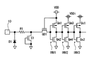
図2は、本発明を適用して好適な半導体集積回路の出力回路の実施例を示す回路図である。
【0037】
この実施例の出力回路は、例えば外部電源仕様が5Vで且つ0.18μCMOSプロセスなどの微細化プロセスにより形成可能な半導体デバイスにおいて、外部出力端子として出力パッドもしくは入力と出力とを兼ねた入出力パッド20に接続されるトライステートの出力回路として適用されるものである。入出力パッド20に入力される信号振幅の許容範囲は例えば0〜7Vである。
【0038】
図2において、20は入力と出力とを兼ねた入出力パッド、D2,D3は規定外の入力信号から内部の回路を保護する保護ダイオード、R2,R3はノイズ除去用の抵抗、Qm5,Qm6は内部回路から信号を受けて入出力パッド20側に信号出力するプッシュプル型出力回路を構成する出力PMOSと出力NMOS、31,32は内部回路から出力MOS Qm5,Qm6のゲート信号を形成する論理ゲート回路、QD3は電源電圧をクランプするデプレッションNMOS、QD4とQN1は入力信号の電圧をクランプするデプレッシNMOSとNMOSである。図示は省略するが、入出力パッド20には、例えば図1に示すような入力回路が別途接続されるものである。図2の出力回路はイネーブル信号/Eがロウレベルのときは、データ信号Dに応じて出力MOS Qm5,Qm6の何れかがオンされて、ハイレベル信号又はロウレベル信号を出力し、イネーブル信号/Eがハイレベルにされると出力MOS Qm5,Qm6がともにオフされて、出力ハイインピーダンス状態となる。
【0039】
上記構成のうち、出力回路を構成するN−PMOS Qm5,Qm6、デプレッションNMOS QD3,QD4、NMOS QN1は、例えば3.3Vの電源電圧で動作するように形成された3V系のMOSFETであり、そのゲート耐圧は5V程度である。
【0040】
出力PMOS Qm5と出力NMOS Qm6から構成される出力回路の動作電源は外部電源電圧VCCをデプレッションNMOS QD3により降圧され且つクランプされた電圧を用いている。
【0041】
電圧クランプ用のデプレッションNMOS QD3は、図1のデプレッションNMOS QD2と同様のもので、プッシュ側の出力PMOS Qm5のソースと外部電源電圧VCCとの間にソース・ドレインが接続される。そして、図1のデプレッションNMOS QD2と同様の作用により出力PMOS Qm5のソース側のノードn3の電位を、おおよそ電源電圧VDDよりしきい値電圧Vthdだけ低い電圧(VDD−Vthd)にクランプすることが出来る。
【0042】
また、入力信号の電圧をクランプするデプレッションNMOS QD4は、入出力パッド20に外部から高電圧(例えば5.0〜7.0V)が印加されたときにこの信号を所定電圧にクランプして出力PMOS Qm5を保護するものである。そして、入出力パッド20と出力PMOS Qm5のドレインとの間にソース・ドレインが接続され、且つ、ゲートに上述の3V系の電源電圧VDD(例えば3.6V)が印加されるように構成される。また、基板電位はグランド電位にされる。
【0043】
このデプレッションNMOS QD4によれば、図1のデプレッションNMOS QD1と同様の作用により、入出力パッド20に高電圧(例えば5.0〜7.0V)が印加された場合でも、出力PMOS Qm5のドレイン側のノードn4の電位を、ほぼ電源電圧VDDよりしきい値電圧Vthdだけ低い電圧(VDD−Vthd)にクランプすることが出来る。それにより出力PMOS Qm5のゲート・ドレイン間電圧を耐圧以下に保つことが出来る。
【0044】
また、信号出力時に出力PMOS Qm5がオン状態にされた際には、デプレッションNMOS QD4はそのソース・ドレイン経路に十分な電流を流して出力ノードn5の電圧を低下させない。
【0045】
この実施例の出力回路のハイレベルの信号は、上記のことからデプレッションMOS QD3によりクランプされた電圧(VDD−Vthd=約3.4V)となる。また、ロウレベルの信号はほぼグランド電位となる。
【0046】
もう一方の入力信号の電圧をクランプするNMOS QN1は、入出力パッド20に外部から高電圧(例えば5.0〜7.0V)が印加されたときにこの信号を所定電圧にクランプして出力NMOS Qm6を保護するものである。そして、入出力パッド20と出力NMOS Qm6のドレインとの間にソース・ドレインが接続され、且つ、ゲートに上述の3V系の電源電圧VDD(例えば3.6V)が印加されるように構成される。また、基板電位はグランド電位にされる。
【0047】
このNMOS QN1によれば、図1のデプレッションNMOS QD1と同様の作用により、入出力パッド20に高電圧(例えば5.0〜7.0V)が印加された場合でも、出力NMOS Qm6のドレイン側のノードn6の電位を、ほぼ電源電圧VDDよりしきい値電圧Vthだけ低い電圧(VDD−Vth)にクランプすることが出来る。それにより出力NMOS Qm6のソース・ドレイン間、ゲート・ドレイン間の電圧を耐圧以下に保つことが出来る。
【0048】
NMOS QN1のしきい値電圧Vthは比較的大きくなるので、クランプ電圧(VDD−Vth)は3V系の電源電圧VDDよりある程度低い値となる。ここでエンハンスメント形のMOSFETを用いているのは、電圧をクランプするノードが出力回路のプル側のノードn6であり、このNMOS QN1による電圧降下が問題にならないからである。従って、デプレッションNMOSにより構成することも出来る。
【0049】
以上のように、この実施例の出力回路によれば、出力回路のプッシュ側に設けられたデプレッションNMOS QD3,QD4とプル側に設けられたNMOSQN1とにより、5V系の外部電源電圧VCCや5V系のハイレベルの入力信号を適宜な電圧にクランプすることができ、それにより0.18μCMOSプロセスのような微細化プロセスで形成される耐圧5Vの出力PMOS Qm5や出力NMOS Qm6を外部電源電圧VCCや5V系の外部入力信号から保護することが出来る。
【0050】
図3は、実施例の入力回路と出力回路とをSRAMに適用した場合の概略構成を示す構成図である。
【0051】
この実施例のSRAM(Static Random Access Memory)は、微細化プロセスにより3V系や1.8V系のMOSFETを用いて外部電源電圧5V仕様に構成したものであり、その入出力回路として本発明に係る入力回路や出力回路が適用されたものである。そして、入出力回路には3V系のMOSFETが使用され、メモリアレイ6やその周辺回路であるアドレスデコーダ回路5やセンスアンプ回路7などには1.8V系のMOSFETが使用されている。
【0052】
この半導体デバイスの内部には、5V系の外部電源電圧VCCを2段階で降圧して、3V系の電源電圧VDDと、1.8V系の電源電圧VDDiとを生成する電源回路2,3が設けられ、入力回路15や出力回路25には3V系の電源電圧VDDが供給され、内部回路には1.8V系の電源電圧VDDiが供給されるようになっている。
【0053】
本発明に係る入力回路15は、SRAMのアドレス信号や制御系信号が入力される入力系に設けられ、出力回路25はデータ信号の入出力系に設けられる。出力回路25に接続される入出力パッド20はデータ信号の入力と出力とが行われる。
【0054】
このようなSRAMによれば、外部電源電圧VCCを2段階で降圧する2つの電源回路2,3を内部に設けるだけで、内部回路や入出力回路を微細化プロセスによる3V系と1.8V系のMOSFETにより形成し、且つ、外部電源電圧5V仕様に対応することが出来る。
【0055】
さらに、出力回路25の駆動源は外部電源電圧VCCであり、入力回路15や出力回路25に供給される電源電圧VDDの駆動能力は小さなもので済むので、電源回路2によるチップサイズの増加分や消費電力は低く抑えることが可能である。それゆえ、例えば0.35μCMOSプロセスなどにより5V仕様のMOSFETを使用してSRAMを形成した場合に比べて、全体のチップサイズを顕著に小さくすることが出来るし、また、消費電力も削減できる。
【0056】
また、微細化プロセスの3V系と1.8V系のMOSFETにより5V仕様のSRAMを形成できるので、5V仕様のSRAM製造工程を3V仕様の微細化プロセスの製造工程へ統合することが出来る。従って、半導体デバイスの製造工程を総合的に合理化することが可能で、それによりコストの大幅な低減も図ることが出来る。また、3V仕様の半導体デバイスと5V仕様のSRAMとをマスタスライス方式により拡散工程まで同一に製造できるので、それにより生産調整も容易なものととなる。
【0057】
また、入力回路15や出力回路25で動作電源をクランプするデプレッションNMOS QD2,QD3が、各入力回路ごと或いは各出力回路ごとに設けられているので、各入力回路間或いは各出力回路間の干渉がなくなり耐ノイズ性が向上されている。
【0058】
図5には、入力回路や出力回路のその他の実施例の回路図を示す。
【0059】
なお、入力回路15や出力回路25で外部電源電圧VCCをクランプするデプレッションNMOS QD2,QD3を各入出力回路に設けずに、図5に示すように1個のデプレッションNMOS QD5を複数の入力回路15Aや出力回路25Aで共有するように構成しても良い。それにより、素子数を減らしてチップ面積をさらに小さくできる。
【0060】
以上本発明者によってなされた発明を実施例に基づき具体的に説明したが、本発明は上記実施例に限定されるものではなく、その要旨を逸脱しない範囲で種々変更可能であることはいうまでもない。
【0061】
例えば、実施例では5V仕様のデバイスを3V仕様の微細化プロセスで形成するための構成として説明したが、その他の外部電源電圧仕様のデバイスに適用することも可能である。
【0062】
また、以上の説明では主として本発明者によってなされた発明をその背景となった利用分野であるSRAMに適用した場合について説明したがこの発明はそれに限定されるものでなく、DRAM(Dynamic Random Access Memory)やフラッシュメモリなどのメモリ一般、論理集積回路、メモリや論理が混載された集積回路装置などに広く利用することができる。
【0063】
【発明の効果】
本願において開示される発明のうち代表的なものによって得られる効果を簡単に説明すれば下記のとおりである。
【0064】
すなわち、本発明の入力回路や出力回路を適用すると、駆動力をあまり必要としない降圧回路を内部に備えるだけで、5V外部電源電圧仕様の半導体デバイスを、微細化プロセスにより形成される1.8V仕様のMOSFETや3V仕様のMOSFETで構成することが可能となり、それにより半導体集積回路のチップサイズを顕著に小さくすることが出来るという効果がある。
【0065】
また、例えば外部電源電圧5V仕様の半導体デバイスの製造工程と微細化プロセスによる例えば外部電源電圧3V仕様の半導体デバイスの製造工程との統合を図り、半導体デバイスの製造工程の総合的な合理化を図ることが可能で、それにより半導体デバイスのコストの大幅な低減を図れるという効果がある。
【図面の簡単な説明】
【図1】本発明を適用して好適な半導体集積回路の入力回路の実施例を示す回路図である。
【図2】本発明を適用して好適な半導体集積回路の出力回路の実施例を示す回路図である。
【図3】実施例の入力回路と出力回路とが適用されたSRAMの概略を示す構成図である。
【図4】入力回路の変形例を示す回路図である。
【図5】入力回路や出力回路のその他の実施例を示す回路図である。
【符号の説明】
2,3 電源回路
10 入力パッド
15 入力回路
20 入出力パッド
25 出力回路
Qm1 入力段のPMOS
Qm2 入力段のNMOS
Qm5 出力PMOS
Qm6 出力NMOS
QD1〜QD4 電圧クランプ用のデプレッションNMOS
QN1 電圧クランプ用のNMOS[0001]
BACKGROUND OF THE INVENTION
The present invention relates to a technique that is useful when applied to an input / output circuit of a semiconductor integrated circuit, and in particular, when a semiconductor device having an external power supply voltage higher than a gate breakdown voltage is formed using a technique for forming an element having a low gate breakdown voltage. Useful technology.
[0002]
[Prior art]
In recent years, semiconductor devices using a miniaturization process such as a 0.18 μm CMOS process are becoming mainstream. In the miniaturization process, 1.8V-type elements and 3V-type elements can be formed. For example, in a semiconductor memory formed by the miniaturization process, 1.8V-type elements are used for the memory cell and its peripheral circuit portion. Therefore, a 3V system element is used for the input / output circuit section.
[0003]
On the other hand, specifications such as an external power supply voltage of 5 V ± 10% are mainly used for devices used in industrial applications, but there is a demand for devices with such specifications to be formed by a miniaturization process. In addition to being able to reduce the chip size according to the miniaturization process, if a device with an external power supply voltage specification of 5V can be manufactured in the manufacturing process of the 0.18 process that is becoming mainstream, the manufacturing process of each other is integrated. Thus, there is an advantage that the manufacturing process of the semiconductor device can be rationalized comprehensively, thereby realizing a significant cost reduction.
[0004]
[Problems to be solved by the invention]
However, in order to form a device having a high external power supply voltage by a miniaturization process, the external power supply voltage is stepped down internally to reduce the 1.8V power supply voltage and the 3V power supply voltage in relation to the breakdown voltage of the element. Must be generated and a power supply voltage suitable for each circuit must be supplied. Specifically, two types of power supply circuits such as regulators are formed in the device to generate the above two systems of power supply voltage, and the core portion of the device formed by the 1.8V system circuit has a 1.8V system. A configuration is conceivable in which a power supply voltage is supplied and a 3V power supply voltage is supplied to an input / output circuit formed by a 3V system circuit.
[0005]
Since the output circuit drives an external load, it needs to be configured to output a relatively large current. Therefore, if the output of the output circuit is obtained from the internal power supply circuit, the driving power of the power supply circuit must also be increased. To realize this with a conventional general power supply circuit, the layout area of the power supply circuit Becomes very large, and the power consumption of the power supply circuit itself becomes very large.
[0006]
SUMMARY OF THE INVENTION An object of the present invention is to make it possible to form a device having an external power supply specification having a large voltage, such as a 5V power supply, using an element with a low withstand voltage formed by a miniaturization process, and a power supply circuit for stepping down the external power supply Another object of the present invention is to provide an input / output circuit of a semiconductor integrated circuit that can operate even when the driving force of the circuit is small.
[0007]
The above and other objects and novel features of the present invention will become apparent from the description of the present specification and the accompanying drawings.
[0008]
[Means for Solving the Problems]
Outlines of representative ones of the inventions disclosed in the present application will be described as follows.
[0009]
That is, the power source of the first power source system having a high voltage and the power source of the second power source system having a low voltage are supplied and connected in series between the high potential point and the low potential point of the first power source system. And an output circuit having a push-pull type output stage having a P-channel MOSFET and an N-channel MOSFET for outputting a signal between the high potential point of the first power supply system and the source of the P-channel MOSFET. A first depletion type N-channel MOSFET (hereinafter abbreviated as first depletion NMOS) having a source and a drain connected to each other and a gate connected to a high potential point of the second power supply system; an external output terminal; A source and a drain are respectively connected between the drain of the P-channel MOSFET, and a gate is connected to a high potential point of the second power supply system. A second depletion type N-channel MOSFET (hereinafter abbreviated as a second depletion NMOS), a source and a drain connected between an external output terminal and the drain of the N-channel MOSFET, and the second power supply system And an N-channel MOSFET having a gate connected to the high potential point.
[0010]
According to such means, the source voltage of the P-channel MOSFET of the push-pull output circuit can be clamped to a value slightly lower than the gate voltage of the first depletion NMOS by the first depletion NMOS. Therefore, even when the withstand voltage of the P-channel MOSFET is less than or equal to the voltage of the first power supply system, the source-drain voltage and the source-gate voltage can be kept below the withstand voltage. In addition, since a depletion type MOSFET is used as the voltage clamping element, the clamp voltage value is not lowered much than the voltage value at the high potential point of the second power supply system applied to the gate of the first depletion NMOS. In addition, the voltage can be clamped stably. Therefore, an output having substantially the same potential as the high potential point of the first power supply system can be obtained from the P-channel MOSFET.
[0011]
Furthermore, when the external output terminal is also used as an input terminal, when a high voltage signal corresponding to the first power supply system such as a 5V high level signal is input to the external output terminal, With the second depletion NMOS, the voltage on the drain side of the P-channel MOSFET can be clamped to a value slightly lower than the gate voltage of the second depletion NMOS. Therefore, even when the withstand voltage of the P-channel MOSFET is less than or equal to the voltage of the input signal, the source-drain voltage and the source-gate voltage can be kept below the withstand voltage. Since a depletion type MOSFET is used as the voltage clamping element here, the output voltage of the P-channel MOSFET can be sent to the external output terminal without much lowering at the time of signal output.
[0012]
Similarly, when a high voltage signal is input to the external output terminal, the voltage on the drain side of the N-channel MOSFET is clamped by the N-channel MOSFET to a voltage lower than the gate voltage of the N-channel MOSFET by a threshold voltage. Is done. Therefore, even if the breakdown voltage of the N-channel MOSFET is less than or equal to the voltage of the input signal, the voltage between the source and drain and between the source and gate can be kept below the breakdown voltage.
[0013]
The input circuit of the present invention is supplied with a power supply of a first power supply system having a high voltage and a power supply of a second power supply system having a low voltage, and has a high potential point and a low potential point of the first power supply system. An input circuit including a P-channel MOSFET having a source and a drain connected to each other and inputting a signal to a gate, the source between the high potential point of the first power supply system and the source of the P-channel MOSFET A third depletion type N-channel MOSFET having a drain connected to each other and a gate connected to a high potential point of the second power supply system; and a source between an external input terminal and the gate of the P-channel MOSFET. A fourth depletion type N-channel MOSFET having a drain connected to each other and a gate connected to a high potential point of the second power supply system is provided.
[0014]
According to such a means, when a high voltage signal corresponding to the first power supply system such as a 5V high level signal is input to the external input terminal, the third depletion NMOS causes the P channel. The voltage on the drain side of the MOSFET can be clamped to a value slightly lower than the gate voltage of the second depletion NMOS. Therefore, even when the withstand voltage of the P-channel MOSFET is less than or equal to the voltage of the input signal, the source-drain voltage and the source-gate voltage can be kept below the withstand voltage. Also, since a depletion type MOSFET is used as the voltage clamping element here, the output voltage output from the P-channel MOSFET to the subsequent circuit when a high level signal is input is supplied to the high potential side of the second power supply system. It does not need to be much lower than the voltage.
[0015]
Similarly, when a high voltage signal is input to the external input terminal, the gate voltage of the P-channel MOSFET can be clamped to a value slightly lower than the gate voltage of the second depletion NMOS by the fourth depletion NMOS. I can do it. Therefore, even when the withstand voltage of the P-channel MOSFET is less than or equal to the voltage of the input signal, the voltage between the gate and the drain can be kept below the withstand voltage. In addition, since a depletion type MOSFET is used as the voltage clamping element here, the gate voltage of the P-channel MOSFET is not lowered much more than the voltage on the high potential side of the second power supply system when a high level signal is input. The P-channel MOSFET can be sufficiently turned on.
[0016]
The input circuit and output circuit of the present invention are applied to an input / output circuit of a semiconductor device, and a power supply circuit for generating a power supply voltage of a second power supply system (for example, 3V system) is provided in the device. By applying a power supply system voltage to the gate of the clamping MOSFET and using an external power supply voltage (for example, 5V system) as a drive source of the output circuit, for example, a semiconductor device having an external power supply voltage specification of 5V Can be formed by a miniaturization process such as a 0.18 μCMOS process, and a power supply circuit provided in the device can be driven less and power consumption can be reduced.
[0017]
Thereby, the chip size of the semiconductor device can be remarkably reduced, and the manufacturing process of the semiconductor device of the first power supply system such as 5V specification can be reduced to that of the second power supply system such as 3V specification by the miniaturization process. It is possible to integrate the manufacturing process of the semiconductor device to comprehensively rationalize the manufacturing process of the semiconductor device, which can greatly reduce the cost.
[0018]
DETAILED DESCRIPTION OF THE INVENTION
Preferred embodiments of the present invention will be described below with reference to the drawings.
[0019]
FIG. 1 is a circuit diagram showing an embodiment of an input circuit of a semiconductor integrated circuit suitable for applying the present invention.
[0020]
The input circuit of this embodiment is applied as an input circuit of a semiconductor device having an external power supply specification of 5 V and can be formed by a miniaturization process such as a 0.18 μCMOS process. The allowable range is, for example, 0 to 7V.
[0021]
In FIG. 1, 10 is an input pad as an external input terminal to which a signal is input from the outside, D1 is a protection diode that protects an internal circuit from an unspecified input signal, and R1 and C1 are resistors provided for noise removal QD1 is a depletion type N-channel MOSFET (hereinafter abbreviated as depletion NMOS) for clamping the voltage of the input signal, QD2 is a depletion NMOS for clamping the power supply voltage, and INV1 is the input signal. Input stage CMOS inverter, INV2 is a CMOS inverter that shifts the signal amplitude to 1.8V system, Qs1 and Qs2 are 1.8V enhancement type P-channel MOSFETs (hereinafter abbreviated as PMOS) constituting the internal circuit of the semiconductor integrated circuit. ) And enhancement type N Yaneru a MOSFET (hereinafter abbreviated as NMOS).
[0022]
Among these, the capacitor C1, the NMOSs Qm2 and Qm4 constituting the inverters INV1 and INV2, the PMOSs Qm1 and Qm3, and the voltage clamping depletion NMOSs QD1 and QD2 are formed to operate with a power supply voltage of 3.3 V, for example. In addition, the gate breakdown voltage is about 5V.
[0023]
Further, the PMOS Qs1 and the NMOS Qs2 which are part of the internal circuit are 1.8V type MOSFETs formed to operate with a power supply voltage VDDi of 1.8V, for example, and the gate withstand voltage is about 3.5V. is there.
[0024]
An external power supply voltage VCC (for example, 4.5 to 7.0 V) is connected to the source side of the PMOS Qm1 in the inverter INV1 in the input stage via a depletion NMOS QD2 for clamping, and the source side of the NMOS Qm2 is connected to the ground. Is done. The output of the inverter INV1 in the input stage is input to the inverter INV2 for level shift in the next stage.
[0025]
The source side of the PMOS Qm3 in the level shift inverter INV2 is supplied with, for example, a 1.8V power supply voltage VDDi (for example, 1.8V) for an internal circuit generated by stepping down the external power supply in the semiconductor integrated circuit. The source side of the NMOS Qm4 is connected to the ground. Then, the output is input to the internal circuit at the subsequent stage. Since the power supply voltage VDDi for the internal circuit is used, the potential of the high level output signal is about 1.8 V corresponding to the element for the internal circuit.
[0026]
A power supply voltage VDDi for the internal circuit is supplied to the internal circuit including the inverter INV3 including the PMOS Qs1 and the NMOS Qs2. The potential of the high level signal to be input / output is about 1.8V, and the potential of the low level signal is 0V.
[0027]
The voltage clamping depletion NMOS QD1 clamps this signal to a predetermined voltage when a high voltage (for example, 5.0 to 7.0 V) is applied from the outside, and causes the inverter INV1 in the input stage to be a high potential external input signal. The power source voltage VDD is generated by connecting the source / drain between the input node n1 of the inverter INV1 and the
[0028]
According to the depletion NMOS QD1 configured as described above, when a high voltage (for example, 5.0 to 7.0 V) is applied to the
[0029]
In addition, after the current flows into the input node of the inverter INV1 and the parasitic capacitance of the gate is charged, the current between the source and drain of the depletion NMOS QD1 is cut off, but a slight leak from the drain of the depletion NMOS QD1 to the substrate. A current flows, whereby the potential of the input node n1 of the inverter INV1 is clamped to a predetermined voltage. The clamp voltage in this case can also be set to a voltage substantially equal to the clamp voltage (VDD−Vthd) when the drain current flows.
[0030]
The other depletion NMOS QD2 for clamping the voltage clamps the power supply voltage on the high potential side of the inverter INV1 in the input stage, so that the external power supply voltage VCC (for example, 4.5 to 7.0 V) higher than the element withstand voltage of the inverter INV1. The inverter INV1 is protected from the source, the source / drain is connected between the source of the PMOS Qm1 and the external power supply voltage VCC, and the internal power supply VDD (for example, 3.6V) is applied to the gate. Configured. The substrate potential is connected to the ground.
[0031]
According to the depletion NMOS QD2 configured in this way, when the inverter INV1 operates, when a current flows from the external power supply VCC side to the PMOS Qm1, a drain current flows to the depletion NMOS QD2, thereby driving the power supply for the inverter INV1. The potential of the node n2 is clamped to a predetermined voltage. The clamp voltage is a voltage (VDD−Vthd) substantially lower than the gate voltage VDD by the threshold voltage Vthd. Here, the threshold voltage Vthd of the depletion NMOS can be formed to a value smaller than that of the enhancement type MOSFET by controlling the channel doping method or the like, and as a result, the clamp voltage can be reduced to about 3.4V. .
[0032]
Further, in a state where the input signal to the inverter INV1 does not change and no current flows between the source and drain of the depletion NMOS QD2, a slight leak current flows from the source to the substrate, thereby driving the power supply node n2 of the inverter INV1. Is clamped to a predetermined voltage. The clamp voltage in this case is also substantially equal to the clamp voltage (VDD−Vthd) when the drain current flows.
[0033]
As described above, according to the input circuit of this embodiment, the depletion NMOSs QD1 and QD2 use the input node n1 of the inverter INV1 in the input stage and the source voltage of the PMOS Qm1 of the inverter INV1 internally. It can be clamped to a voltage slightly lower than the generated 3V system power supply voltage VDD, so that the MOS Qm1 and Qm2 having a breakdown voltage of 5V or less formed by a miniaturization process such as the 0.18 μCMOS process can be It is possible to protect from external input signals and external power supply voltage VCC.
[0034]
FIG. 4 shows a modification of the input circuit of FIG.
[0035]
The operation voltage of the inverter INV1 in the input stage is not obtained by stepping down the external power supply voltage VCC by the depletion NMOS, but is directly supplied with the internal power supply VDD as the operation power supply as shown in FIG. It is also good. Since the threshold voltage Vthd of the depletion NMOS varies due to process variations, the clamp voltage due to the depletion NMOS also varies due to process variations. By directly supplying the power supply voltage VDD in this way, the output amplitude of the inverter INV1 in the input stage can be increased. It is possible to stabilize and transmit the signal to the subsequent stage.
[0036]
FIG. 2 is a circuit diagram showing an embodiment of an output circuit of a semiconductor integrated circuit suitable for applying the present invention.
[0037]
The output circuit of this embodiment is, for example, an output pad or an input / output pad serving as both an input and an output as an external output terminal in a semiconductor device having an external power supply specification of 5 V and capable of being formed by a miniaturization process such as 0.18 μCMOS process. 20 is applied as a tri-state output circuit connected to 20. The allowable range of the signal amplitude input to the input /
[0038]
In FIG. 2, 20 is an input / output pad that serves both as input and output, D2 and D3 are protective diodes that protect internal circuits from unspecified input signals, R2 and R3 are noise removal resistors, and Qm5 and Qm6 are An output PMOS and an output NMOS, 31 and 32 that constitute a push-pull type output circuit that receives a signal from the internal circuit and outputs the signal to the input /
[0039]
Among the above-described configurations, the N-PMOS Qm5, Qm6, depletion NMOS QD3, QD4, and NMOS QN1 constituting the output circuit are, for example, 3V type MOSFETs configured to operate with a power supply voltage of 3.3V. The gate breakdown voltage is about 5V.
[0040]
The operating power supply of the output circuit composed of the output PMOS Qm5 and the output NMOS Qm6 uses a voltage obtained by stepping down and clamping the external power supply voltage VCC by the depletion NMOS QD3.
[0041]
The voltage clamping depletion NMOS QD3 is the same as the depletion NMOS QD2 in FIG. 1, and the source and drain are connected between the source of the push-side output PMOS Qm5 and the external power supply voltage VCC. The potential of the node n3 on the source side of the output PMOS Qm5 can be clamped to a voltage (VDD−Vthd) approximately lower than the power supply voltage VDD by the threshold voltage Vthd by the same operation as the depletion NMOS QD2 of FIG. .
[0042]
The depletion NMOS QD4 that clamps the voltage of the input signal clamps this signal to a predetermined voltage when an external high voltage (for example, 5.0 to 7.0 V) is applied to the input /
[0043]
According to the depletion NMOS QD4, the drain side of the output PMOS Qm5 can be operated even when a high voltage (for example, 5.0 to 7.0 V) is applied to the input /
[0044]
In addition, when the output PMOS Qm5 is turned on at the time of signal output, the depletion NMOS QD4 does not reduce the voltage of the output node n5 by causing a sufficient current to flow through the source / drain path.
[0045]
The high level signal of the output circuit of this embodiment is the voltage (VDD−Vthd = about 3.4 V) clamped by the depletion MOS QD3. The low level signal is almost at the ground potential.
[0046]
The NMOS QN1, which clamps the voltage of the other input signal, clamps this signal to a predetermined voltage when an external high voltage (for example, 5.0 to 7.0 V) is applied to the input /
[0047]
According to this NMOS QN1, even when a high voltage (for example, 5.0 to 7.0 V) is applied to the input /
[0048]
Since the threshold voltage Vth of the NMOS QN1 is relatively large, the clamp voltage (VDD−Vth) is a value that is somewhat lower than the 3V power supply voltage VDD. The enhancement type MOSFET is used here because the node for clamping the voltage is the node n6 on the pull side of the output circuit, and this voltage drop due to the NMOS QN1 does not become a problem. Therefore, it can be constituted by a depletion NMOS.
[0049]
As described above, according to the output circuit of this embodiment, the depletion NMOSs QD3 and QD4 provided on the push side of the output circuit and the NMOS QN1 provided on the pull side allow the 5V external power supply voltage VCC and 5V The high-level input signal can be clamped to an appropriate voltage, whereby the output PMOS Qm5 and the output NMOS Qm6 with a withstand voltage of 5V formed by a miniaturization process such as the 0.18 μCMOS process can be used as the external power supply voltage VCC or 5V. It can protect against external input signals of the system.
[0050]
FIG. 3 is a configuration diagram showing a schematic configuration when the input circuit and the output circuit of the embodiment are applied to the SRAM.
[0051]
The SRAM (Static Random Access Memory) of this embodiment is configured to have an external power supply voltage 5 V specification by using a 3 V or 1.8 V MOSFET by a miniaturization process, and an input / output circuit according to the present invention. An input circuit and an output circuit are applied. A 3V type MOSFET is used for the input / output circuit, and a 1.8V type MOSFET is used for the memory array 6 and its peripheral circuits, such as the address decoder circuit 5 and the sense amplifier circuit 7.
[0052]
Inside this semiconductor device, there are provided power supply circuits 2 and 3 for stepping down the 5V external power supply voltage VCC in two stages to generate a 3V power supply voltage VDD and a 1.8V power supply voltage VDDi. The
[0053]
The
[0054]
According to such an SRAM, only by providing two power supply circuits 2 and 3 for stepping down the external power supply voltage VCC in two stages, the internal circuit and the input / output circuit are 3V system and 1.8V system by a miniaturization process. It is possible to correspond to the external power supply voltage 5V specification.
[0055]
Further, the drive source of the
[0056]
In addition, since the 5V-specific SRAM can be formed by the 3V-type and 1.8V-type MOSFETs in the miniaturization process, the 5V-specific SRAM manufacturing process can be integrated into the 3V-specific miniaturization process. Therefore, it is possible to comprehensively rationalize the manufacturing process of the semiconductor device, and thereby to greatly reduce the cost. In addition, since the 3V specification semiconductor device and the 5V specification SRAM can be manufactured in the same way up to the diffusion process by the master slice method, the production adjustment is also facilitated.
[0057]
In addition, since the depletion NMOSs QD2 and QD3 for clamping the operation power supply by the
[0058]
FIG. 5 shows a circuit diagram of another embodiment of the input circuit and the output circuit.
[0059]
Note that the depletion NMOSs QD2 and QD3 for clamping the external power supply voltage VCC by the
[0060]
The invention made by the present inventor has been specifically described based on the embodiments. However, the present invention is not limited to the above embodiments, and various modifications can be made without departing from the scope of the invention. Nor.
[0061]
For example, in the embodiment, the configuration for forming a 5V specification device by a 3V specification miniaturization process has been described, but the present invention can also be applied to other external power supply voltage specification devices.
[0062]
Further, in the above description, the case where the invention made by the present inventor is applied to the SRAM which is the field of use as the background has been described. However, the present invention is not limited to this, and DRAM (Dynamic Random Access Memory) ) And a flash memory, etc., a general memory, a logic integrated circuit, an integrated circuit device in which a memory and logic are mixedly mounted, and the like.
[0063]
【The invention's effect】
The effects obtained by the representative ones of the inventions disclosed in the present application will be briefly described as follows.
[0064]
That is, when the input circuit or output circuit of the present invention is applied, a semiconductor device having a 5V external power supply voltage specification is formed by a miniaturization process by merely including a step-down circuit that does not require much driving force. It is possible to configure with a specification MOSFET or a 3V specification MOSFET, which has the effect of significantly reducing the chip size of the semiconductor integrated circuit.
[0065]
Also, for example, by integrating the manufacturing process of a semiconductor device having an external power supply voltage specification of 5V and the manufacturing process of a semiconductor device having an external power supply voltage specification of 3V by a miniaturization process, the manufacturing process of the semiconductor device is rationalized. Therefore, the cost of the semiconductor device can be greatly reduced.
[Brief description of the drawings]
FIG. 1 is a circuit diagram showing an embodiment of an input circuit of a semiconductor integrated circuit suitable for application of the present invention.
FIG. 2 is a circuit diagram showing an embodiment of an output circuit of a semiconductor integrated circuit suitable for applying the present invention.
FIG. 3 is a configuration diagram illustrating an outline of an SRAM to which an input circuit and an output circuit of an embodiment are applied;
FIG. 4 is a circuit diagram showing a modification of the input circuit.
FIG. 5 is a circuit diagram showing another embodiment of the input circuit and the output circuit.
[Explanation of symbols]
2, 3 Power supply circuit
10 Input pad
15 Input circuit
20 I / O pads
25 Output circuit
PMOS of Qm1 input stage
NMOS of Qm2 input stage
Qm5 output PMOS
Qm6 output NMOS
Depletion NMOS for QD1 to QD4 voltage clamp
NMOS for QN1 voltage clamp
Claims (2)
上記第1電源系の高電位点と上記PチャネルMOSFETのソースとの間にソースとドレインとがそれぞれ接続され、且つ、上記第2電源系の高電位点にゲートが接続された第1のデプレッション形NチャネルMOSFETと、
外部出力端子と上記PチャネルMOSFETのドレインとの間にソースとドレインとがそれぞれ接続され、且つ、上記第2電源系の高電位点にゲートが接続された第2のデプレッション形NチャネルMOSFETと、
外部出力端子と上記第1NチャネルMOSFETのドレインとの間にソースとドレインとがそれぞれ接続され、且つ、上記第2電源系の高電位点にゲートが接続された第2NチャネルMOSFETと、
を備えたことを特徴とする出力回路。The power supply of the first power supply system having the same or higher gate breakdown voltage and voltage of the MOSFET and the depletion type MOSFET constituting the circuit and the second power supply system power supply having a voltage lower than the gate breakdown voltage are supplied. An output circuit having a push-pull type output stage having a P-channel MOSFET and a first N-channel MOSFET that are connected in series between a high potential point and a low potential point of a single power supply system and that output a signal. And
A first depletion in which a source and a drain are connected between a high potential point of the first power supply system and a source of the P-channel MOSFET, and a gate is connected to the high potential point of the second power supply system. N-channel MOSFET,
A second depletion type N-channel MOSFET having a source and a drain connected between an external output terminal and the drain of the P-channel MOSFET, and a gate connected to a high potential point of the second power supply system;
Is connected to the source and drain, respectively between the drain of the external output terminal and the first 1 N-channel MOSFET, and a second 2 N-channel MOSFET having a gate connected to the high potential point of the second power supply system,
An output circuit comprising:
上記第1電源系の高電位点と上記PチャネルMOSFETのソースとの間にソースとドレインとがそれぞれ接続され、且つ、上記第2電源系の高電位点にゲートが接続された第3のデプレッション形NチャネルMOSFETと、
外部入力端子と上記PチャネルMOSFETのゲートとの間にソースとドレインとがそれぞれ接続され、且つ、上記第2電源系の高電位点にゲートが接続された第4のデプレッション形NチャネルMOSFETと、
を備え、
前記外部入力端子に前記第1電源系の電圧と同等の電圧レベルの入力信号を入力可能としたことを特徴とする入力回路。The power supply of the first power supply system having the same or higher gate breakdown voltage and voltage of the MOSFET and the depletion type MOSFET constituting the circuit and the second power supply system power supply having a voltage lower than the gate breakdown voltage are supplied. An input circuit including a P-channel MOSFET in which a source and a drain are connected between a high potential point and a low potential point of a single power supply system, and a signal is input to a gate,
A third depletion in which a source and a drain are connected between a high potential point of the first power supply system and a source of the P-channel MOSFET, and a gate is connected to the high potential point of the second power supply system. N-channel MOSFET,
A fourth depletion-type N-channel MOSFET having a source and a drain connected between the external input terminal and the gate of the P-channel MOSFET, and a gate connected to a high potential point of the second power supply system;
Equipped with a,
An input circuit, wherein an input signal having a voltage level equivalent to the voltage of the first power supply system can be input to the external input terminal .
Priority Applications (1)
| Application Number | Priority Date | Filing Date | Title |
|---|---|---|---|
| JP2000330274A JP3838482B2 (en) | 2000-10-30 | 2000-10-30 | Output circuit and input circuit |
Applications Claiming Priority (1)
| Application Number | Priority Date | Filing Date | Title |
|---|---|---|---|
| JP2000330274A JP3838482B2 (en) | 2000-10-30 | 2000-10-30 | Output circuit and input circuit |
Publications (3)
| Publication Number | Publication Date |
|---|---|
| JP2002135104A JP2002135104A (en) | 2002-05-10 |
| JP2002135104A5 JP2002135104A5 (en) | 2005-06-16 |
| JP3838482B2 true JP3838482B2 (en) | 2006-10-25 |
Family
ID=18806826
Family Applications (1)
| Application Number | Title | Priority Date | Filing Date |
|---|---|---|---|
| JP2000330274A Expired - Fee Related JP3838482B2 (en) | 2000-10-30 | 2000-10-30 | Output circuit and input circuit |
Country Status (1)
| Country | Link |
|---|---|
| JP (1) | JP3838482B2 (en) |
Families Citing this family (3)
| Publication number | Priority date | Publication date | Assignee | Title |
|---|---|---|---|---|
| JP2004023402A (en) * | 2002-06-14 | 2004-01-22 | Ricoh Co Ltd | Io cell circuit |
| JP2005122832A (en) | 2003-10-17 | 2005-05-12 | Renesas Technology Corp | Semiconductor integrated circuit device |
| US7391193B2 (en) * | 2005-01-25 | 2008-06-24 | Sandisk Corporation | Voltage regulator with bypass mode |
Family Cites Families (10)
| Publication number | Priority date | Publication date | Assignee | Title |
|---|---|---|---|---|
| JPS59112725A (en) * | 1982-12-17 | 1984-06-29 | Sanyo Electric Co Ltd | Semiconductor device |
| JPH0685497B2 (en) * | 1985-12-20 | 1994-10-26 | 株式会社東芝 | Semiconductor integrated circuit |
| JPH0522109A (en) * | 1991-07-12 | 1993-01-29 | Nec Corp | Microcomputer |
| JP2819950B2 (en) * | 1992-07-28 | 1998-11-05 | 日本電気株式会社 | Output circuit |
| JPH06232728A (en) * | 1993-02-03 | 1994-08-19 | Nec Corp | Input output circuit |
| JPH06244710A (en) * | 1993-02-16 | 1994-09-02 | Sharp Corp | Outputting circuit for semiconductor integrated circuit |
| JPH06260927A (en) * | 1993-03-08 | 1994-09-16 | Nippon Telegr & Teleph Corp <Ntt> | Logic circuit for complementary field-effect transistor |
| JP2901171B2 (en) * | 1993-10-08 | 1999-06-07 | 日本電信電話株式会社 | Deep submicron MOSFET output buffer circuit |
| JPH08148986A (en) * | 1994-11-21 | 1996-06-07 | Mitsubishi Electric Corp | Output buffer circuit |
| JP3580062B2 (en) * | 1995-12-20 | 2004-10-20 | セイコーエプソン株式会社 | Bus line driving circuit and semiconductor memory device having the same |
-
2000
- 2000-10-30 JP JP2000330274A patent/JP3838482B2/en not_active Expired - Fee Related
Also Published As
| Publication number | Publication date |
|---|---|
| JP2002135104A (en) | 2002-05-10 |
Similar Documents
| Publication | Publication Date | Title |
|---|---|---|
| KR0155078B1 (en) | Semiconductor circuit having cmos circuit for use in strong electric field | |
| KR100363142B1 (en) | Semiconductor Integrated Circuits with Three-State Logic Circuits | |
| US20070121358A1 (en) | Semiconductor integrated circuit | |
| KR100644224B1 (en) | Level shifter for reducing leakage current and block driver in nonvolatile semiconductor memory device having the same | |
| US20060279346A1 (en) | Semiconductor integrated circuit | |
| KR100471737B1 (en) | Output circuits, circuits to reduce leakage currents, methods for selectively switching transistors and semiconductor memory | |
| US20080284504A1 (en) | Semiconductor integrated circuit | |
| US6225852B1 (en) | Use of biased high threshold voltage transistor to eliminate standby current in low voltage integrated circuits | |
| US20080001656A1 (en) | Semiconductor integrated circuit | |
| US9054700B2 (en) | Apparatus and methods of driving signal for reducing the leakage current | |
| US6128230A (en) | Semiconductor memory with PN junction potential reduction in a writing mode | |
| US7598794B1 (en) | Well bias architecture for integrated circuit device | |
| JPH0865135A (en) | Output buffer circuit | |
| JPH10173499A (en) | Output driver circuit and semiconductor device | |
| JPH08203270A (en) | Semiconductor integrated circuit | |
| JP3838482B2 (en) | Output circuit and input circuit | |
| JP3554638B2 (en) | Semiconductor circuit | |
| US5808934A (en) | Integrated logic circuit and EEPROM | |
| US6459556B1 (en) | Input buffer | |
| US7667521B2 (en) | Voltage switch circuit of semiconductor device | |
| US6028800A (en) | Sense amplifier driver having variable power-supply voltage | |
| JPH09245482A (en) | Logic circuit and semiconductor memory | |
| JP2003298410A (en) | Semiconductor integrated circuit | |
| JP2913379B2 (en) | Write circuit for nonvolatile memory | |
| US6570811B1 (en) | Writing operation control circuit and semiconductor memory using the same |
Legal Events
| Date | Code | Title | Description |
|---|---|---|---|
| A711 | Notification of change in applicant |
Free format text: JAPANESE INTERMEDIATE CODE: A712 Effective date: 20030725 |
|
| A521 | Written amendment |
Free format text: JAPANESE INTERMEDIATE CODE: A523 Effective date: 20040924 |
|
| A621 | Written request for application examination |
Free format text: JAPANESE INTERMEDIATE CODE: A621 Effective date: 20040924 |
|
| A521 | Written amendment |
Free format text: JAPANESE INTERMEDIATE CODE: A523 Effective date: 20040924 |
|
| A977 | Report on retrieval |
Free format text: JAPANESE INTERMEDIATE CODE: A971007 Effective date: 20060313 |
|
| A131 | Notification of reasons for refusal |
Free format text: JAPANESE INTERMEDIATE CODE: A131 Effective date: 20060413 |
|
| A521 | Written amendment |
Free format text: JAPANESE INTERMEDIATE CODE: A523 Effective date: 20060609 |
|
| TRDD | Decision of grant or rejection written | ||
| A01 | Written decision to grant a patent or to grant a registration (utility model) |
Free format text: JAPANESE INTERMEDIATE CODE: A01 Effective date: 20060629 |
|
| A61 | First payment of annual fees (during grant procedure) |
Free format text: JAPANESE INTERMEDIATE CODE: A61 Effective date: 20060629 |
|
| A61 | First payment of annual fees (during grant procedure) |
Free format text: JAPANESE INTERMEDIATE CODE: A61 Effective date: 20060727 |
|
| R150 | Certificate of patent or registration of utility model |
Free format text: JAPANESE INTERMEDIATE CODE: R150 |
|
| FPAY | Renewal fee payment (event date is renewal date of database) |
Free format text: PAYMENT UNTIL: 20090811 Year of fee payment: 3 |
|
| FPAY | Renewal fee payment (event date is renewal date of database) |
Free format text: PAYMENT UNTIL: 20100811 Year of fee payment: 4 |
|
| FPAY | Renewal fee payment (event date is renewal date of database) |
Free format text: PAYMENT UNTIL: 20110811 Year of fee payment: 5 |
|
| FPAY | Renewal fee payment (event date is renewal date of database) |
Free format text: PAYMENT UNTIL: 20110811 Year of fee payment: 5 |
|
| S111 | Request for change of ownership or part of ownership |
Free format text: JAPANESE INTERMEDIATE CODE: R313115 |
|
| FPAY | Renewal fee payment (event date is renewal date of database) |
Free format text: PAYMENT UNTIL: 20110811 Year of fee payment: 5 |
|
| R350 | Written notification of registration of transfer |
Free format text: JAPANESE INTERMEDIATE CODE: R350 |
|
| FPAY | Renewal fee payment (event date is renewal date of database) |
Free format text: PAYMENT UNTIL: 20120811 Year of fee payment: 6 |
|
| FPAY | Renewal fee payment (event date is renewal date of database) |
Free format text: PAYMENT UNTIL: 20120811 Year of fee payment: 6 |
|
| FPAY | Renewal fee payment (event date is renewal date of database) |
Free format text: PAYMENT UNTIL: 20130811 Year of fee payment: 7 |
|
| S531 | Written request for registration of change of domicile |
Free format text: JAPANESE INTERMEDIATE CODE: R313531 |
|
| R350 | Written notification of registration of transfer |
Free format text: JAPANESE INTERMEDIATE CODE: R350 |
|
| LAPS | Cancellation because of no payment of annual fees |