JP3832947B2 - Data transfer memory device - Google Patents
Data transfer memory device Download PDFInfo
- Publication number
- JP3832947B2 JP3832947B2 JP31392797A JP31392797A JP3832947B2 JP 3832947 B2 JP3832947 B2 JP 3832947B2 JP 31392797 A JP31392797 A JP 31392797A JP 31392797 A JP31392797 A JP 31392797A JP 3832947 B2 JP3832947 B2 JP 3832947B2
- Authority
- JP
- Japan
- Prior art keywords
- data
- memory
- output
- memory device
- memory module
- Prior art date
- Legal status (The legal status is an assumption and is not a legal conclusion. Google has not performed a legal analysis and makes no representation as to the accuracy of the status listed.)
- Expired - Fee Related
Links
Images


Classifications
-
- G—PHYSICS
- G06—COMPUTING; CALCULATING OR COUNTING
- G06F—ELECTRIC DIGITAL DATA PROCESSING
- G06F13/00—Interconnection of, or transfer of information or other signals between, memories, input/output devices or central processing units
- G06F13/38—Information transfer, e.g. on bus
- G06F13/42—Bus transfer protocol, e.g. handshake; Synchronisation
- G06F13/4204—Bus transfer protocol, e.g. handshake; Synchronisation on a parallel bus
- G06F13/4234—Bus transfer protocol, e.g. handshake; Synchronisation on a parallel bus being a memory bus
- G06F13/4243—Bus transfer protocol, e.g. handshake; Synchronisation on a parallel bus being a memory bus with synchronous protocol
-
- G—PHYSICS
- G11—INFORMATION STORAGE
- G11C—STATIC STORES
- G11C11/00—Digital stores characterised by the use of particular electric or magnetic storage elements; Storage elements therefor
- G11C11/21—Digital stores characterised by the use of particular electric or magnetic storage elements; Storage elements therefor using electric elements
- G11C11/34—Digital stores characterised by the use of particular electric or magnetic storage elements; Storage elements therefor using electric elements using semiconductor devices
-
- Y—GENERAL TAGGING OF NEW TECHNOLOGICAL DEVELOPMENTS; GENERAL TAGGING OF CROSS-SECTIONAL TECHNOLOGIES SPANNING OVER SEVERAL SECTIONS OF THE IPC; TECHNICAL SUBJECTS COVERED BY FORMER USPC CROSS-REFERENCE ART COLLECTIONS [XRACs] AND DIGESTS
- Y02—TECHNOLOGIES OR APPLICATIONS FOR MITIGATION OR ADAPTATION AGAINST CLIMATE CHANGE
- Y02D—CLIMATE CHANGE MITIGATION TECHNOLOGIES IN INFORMATION AND COMMUNICATION TECHNOLOGIES [ICT], I.E. INFORMATION AND COMMUNICATION TECHNOLOGIES AIMING AT THE REDUCTION OF THEIR OWN ENERGY USE
- Y02D10/00—Energy efficient computing, e.g. low power processors, power management or thermal management
Description
【0001】
【発明の属する技術分野】
本発明は、バスシステム内の一つのシステムバス上でデータを転送する機能を有する複数のDRAM(ダイミック・ランダムアクセスメモリ)等の複数のメモリデバイスや、このようなメモリデバイスがそれぞれ搭載された複数個のメモリモジュールから構成されるデータ転送メモリ装置に関する。
【0002】
一般に、バスシステムにおいては、システム全体の効率を高めるために、複数のメモリデバイスまたは複数のメモリモジュールとCPU(中央処理装置)等との間で各種のデータの入出力を高速にて行うことが要求される。
本発明は、複数のメモリデバイスをシステムバス上に配置するか、または、このような複数のメモリデバイスが搭載されたメモリモジュールを複数個システムバス上に配置して形成されるデータ転送メモリ装置において、各々のメモリデバイスまたはメモリモジュールに対する入出力の対象となる各種のデータを、システムバスのバスラインを介して高速にてかつ途切れなく転送するための一手法について言及するものである。
【0003】
【従来の技術】
以下、図19〜図21を参照しながら、従来方式によるデータ転送メモリ装置を使用したバスシステムの構成を説明する。
図19は、従来の第1例に係るバスシステムの構成を示すブロック図である。ここでは、ランバス(Rambus)方式により動作する複数のランバスDRAMからなるメモリデバイス、または、このようなメモリデバイスが搭載された複数のメモリモジュールを含むバスシステムの構成を例示する。ただし、ここでは、システムバス7のデータ転送用バスライン(通常、DQラインと称する)は省略する。
【0004】
図19においては、CPU等からなる一つのチップセット(チップセット♯0)40と、基準信号発生器42と、第1のメモリデバイスまたはメモリモジュール〜第mのメモリデバイスまたはメモリモジュール100−1、100−2、……、100−m(以下、複数のメモリデバイスまたはメモリモジュール100−1〜100−mと略記する:mは任意の正の整数)とが、システムバス7のクロックラインに接続されている。このクロックラインでは、複数のメモリデバイスまたはメモリモジュール100−1〜100−mからチップセット40へ向かうデータ出力用クロックラインと、チップセット40から複数のメモリデバイスまたはメモリモジュール100−1〜100−mへ向かうデータ入力用クロックラインとを折り返して構成されている。
【0005】
ここでは、データ出力用クロックラインを介してトランスファクロック(Transfer Clock)T−CLKが転送されると共に、データ入力用クロックラインを介してレシーブクロック(Receive Clock )R−CLKが転送される。すなわち、この場合は、同一のクロックラインのみを使用して上記のトランスファクロックT−CLKおよびレシーブクロックR−CLKを転送することによって、各メモリデバイスまたは各メモリモジュールへのデータ入力と各メモリデバイスまたは各メモリモジュールからのデータ出力の位相のずれをなくすようにしている。このクロックライン上の信号のレベルは、電源Vtよりレベル調整用抵抗Rt1を介して供給される電圧により調整される。
【0006】
図19に示す従来の第1例のバスシステムでは、複数のメモリデバイスまたはメモリモジュールからチップセット40へのデータ出力は、どのランバスRAM等にアクセスしても同一タイミングになっている。ただし、システムバスのバスラインの長さを示すシステムバス長Lによる信号遅延時間τがデータ転送時間の半分以上になると、レシーブクロックR−CLKによるプロトコル入力からトランスファクロックT−CLKによるデータ出力までの時間が不足する。このため、システムバス長Lの上限値が制限され、データ転送速度が増加して高速になるほど、システムバス長Lを短くしなければならなくなる。
【0007】
また一方で、アクノリッジパケットがチップセットへ到着する時間を監視することによって、チップセットがデータの到着をあらかじめ知ることができる。ただし、上記アクノリッジパケットがチップセットへ到着する時間は、各々のメモリデバイスまたはメモリモジュールからの距離で決まるため、チップセットはその時間だけ待たなければならなくなる。
【0008】
図20は、従来の第2例に係るバスシステムの構成を示すブロック図である。ここでは、DQストローブ(DQ Strobe )方式により動作する複数のメモリデバイス、または、このようなメモリデバイスが搭載された複数のメモリモジュールを含むバスシステムの構成を例示する。ただし、ここでも、システムバス7のDQラインは省略する。
【0009】
図20において、システムバス7のバスラインは、CPU等の一つのチップセット40から、第1のメモリデバイスまたはメモリモジュール〜第mのメモリデバイスまたはメモリモジュール110−1、110−2、……、110−m(以下、複数のメモリデバイスまたはメモリモジュール110−1〜110−mと略記する)へ向かうメインクロックMCLKを転送するためのMCLKラインと、データ出力時に複数のメモリデバイスまたはメモリモジュール110−1〜110−mの各々からデータを出力するときに発信されるDQストローブ信号DQSを転送するためのDQSラインとを含む。上記MCLKライン上の信号のレベルは、電源Vtよりレベル調整用抵抗Rt2を介して供給される電圧により調整され、上記DQSライン上の信号のレベルは、電源Vtより他のレベル調整用抵抗Rt3を介して供給される電圧により調整される。
【0010】
さらに、図20においては、チップセット40と、基準信号発生器42と、複数のメモリデバイスまたはメモリモジュール110−1〜110−mとが、上記のMCLKラインおよびDQSラインに接続されている。
図20に示す従来の第2例のバスシステムでは、メインクロックMCLKに同期して複数のメモリデバイスまたはメモリモジュール110−1〜110−mが、入力されるデータを受け取る。また一方で、複数のメモリデバイスまたはメモリモジュールからのデータ出力時(すなわち、データ読み出し時)には、各々のメモリデバイスまたはメモリモジュールにより生成されるDQストローブ信号DQSに同期してデータが出力される。
【0011】
さらに、複数のメモリデバイスまたはメモリモジュールへのデータ入力時(すなわち、データ書き込み時)にもチップセット40からDQストローブ信号用端子を制御し、このDQストローブ信号用端子を制御するタイミングに同期して複数のメモリデバイスまたはメモリモジュールが、入力されるデータを受け取る方法もある。
【0012】
この方法では、システムバス長Lによる信号遅延時間τが生ずるので、メモリデバイスまたはメモリモジュールの位置により同メモリデバイスまたはメモリモジュールがデータ読み出し用のリード命令を受け取る時間や、メモリデバイスまたはメモリモジュールから出力されるデータをチップセット40が受け取る時間がまちまちになる。この場合、チップセット40がリード命令を発行してから同チップセット40が最初にデータを受け取るまでに要するファーストアクセス・タイム(ファーストアクセス時間)は、チップセット40から制御することができないため、同チップセット40は、メモリデバイスまたはメモリモジュールから出力されるデータに応じてデータ取り込みウィンドウの位置を変えなければならなくなる。
【0013】
特に、チップセット40から最も近い位置にある第1のメモリデバイスまたはメモリモジュールデバイス110─1から出力されるデータを受け取る時間と、チップセット40から最も遠い位置にある第mのメモリデバイスまたはメモリモジュールデバイス110─mから出力されるデータを受け取る時間とは大きく異なるため、チップセット40では、これらのメモリデバイスまたはメモリモジュールデバイスからデータを受け取る度に、データ取り込みウィンドウの位置をいちいち設定し直すことが必要になる。
【0014】
図21は、従来の第3例に係るバスシステムの構成を示すブロック図である。ここでは、リターンクロック(Return Clock)方式により動作するような、複数のメモリデバイスがそれぞれ搭載された複数のメモリモジュールを含むバスシステムの構成を例示する。
図21において、システムバス7のバスラインは、データ入力時に、チップセット40から、第1のメモリモジュール〜第mのメモリモジュール120−1、120−2、……、120−m(以下、複数のメモリモジュール120−1〜120−mと略記する)へ向かうメインクロックMCLKを転送するためのMCLKラインと、データ出力時に、複数のメモリモジュール120−1〜120−mからチップセット40へ向かうリターンクロック(Return Clock)RCLKを転送するためのRCLKラインとを含む。上記MCLKライン上の信号のレベルは、電源Vtよりレベル調整用抵抗Rt4を介して供給される電圧により調整され、上記RCLKライン上の信号のレベルは、電源Vtより他のレベル調整用抵抗Rt5を介して供給される電圧により調整される。
【0015】
図21においても、図19に示した従来の第1例と同じように、CPU等からなる一つのチップセット40と、基準信号発生器42と、複数のメモリモジュール120−1〜120−mとが、システムバス7のMCLKラインやRCLKラインやDQライン等に接続されている。
ただし、図21の従来の第3例のバスシステムでは、図19に示した従来の第1例と異なり、各々のメモリモジュール120−1〜120−m内に、クロック位相調整用のDLL(ディレイド・ロック・ループ(Delayed Lock Loop )の略)500とバッファアンプ510とを含むモジュールバッファを設けている。さらに、メモリモジュール内の各半導体素子を駆動するための電源Vccが、レベル調整用抵抗Rpmを介して、チップセット40から最も遠い位置にあるメモリモジュール120−mのイネーブル端子ENに接続されている。
【0016】
この場合、チップセット40から転送されるメインクロックMCLKに応じて、上記メモリモジュール120−m内のモジュールバッファが、イネーブル端子ENのレベルの状態(ここでは、電源Vccによる電源電圧レベル)に基づき活性化される。このようにして活性化されたモジュールバッファは、メインクロックMCLKを受け取り、DLL510にて同メインクロックMCLKの位相補正を行う。このメインクロックMCLKは、位相補正を行った後に、リターンクロックRCLKとして、各々のメモリモジュールに搭載された複数のメモリデバイスのデータ出力用のクロックとして用いられる。すなわち、この場合は、図19に示した従来の第1例のトランファクロックT−CLKの代わりに、メモリモジュールそのものからリターンクロックRCLKを生成している。上記のリターンクロック方式では、従来の第1例のランバス方式と同様に、どのメモリモジュールにアクセスした場合でも、当該メモリモジュールから出力されるデータは、同一タイミングにてチップセット40に到達する。
【0017】
しかしながら、このようなリターンクロック方式においても、システムバス長Lによる信号遅延時間τがデータ転送時間の半分以上になると、従来の第1例のランバス方式と同様に、チップセット40から最も近い位置にあるメモリモジュール120−1のデータと、最も遠い位置にあるメモリモジュール120−mのデータとのアクセス時間に差が生じてくる。
【0018】
【発明が解決しようとする課題】
上記のとおり、従来の第1例のバスシステムでは、システムバスのバスライン長により生ずる信号遅延時間が大きくなると、チップセットから最も遠い位置にあるメモリデバイスからデータが到達するのをチップセットにて待つ時間が長くなる。このため、高速にてデータを転送することが困難になり、システム全体の効率が低下するという問題が発生する。
【0019】
さらに、従来の第2例のバスシステムでは、システムバスのバスライン長により生ずる信号遅延時間が大きくなると、メモリデバイスまたはメモリモジュールから出力されるデータをチップセットが受け取る時間がまちまちになる。このため、メモリデバイスまたはメモリモジュールのチップセットに対する相対的な位置に応じてチップセット内のデータ取り込みウィンドウの位置を変えなければならなくなるので、システム全体の効率が低下するという問題が発生する。
【0020】
さらにまた、従来の第3例のバスシステムでは、システムバスのバスライン長により生ずる信号遅延時間がデータ転送時間の半分以上になると、従来の第1例の場合と同様に、チップセットから最も近い位置のメモリモジュールのデータが同チップセットに到達するまでの時間と、最も遠い位置のメモリモジュールのデータが同チップセットに到達するまでの時間との間に差が生じてくる。このため、従来の第1例の場合と同様に、高速にてデータを転送することが困難になり、システム全体の効率が低下するという問題が発生する。
【0021】
本発明は上記問題点に鑑みてなされたものであり、複数のメモリデバイスまたは複数のメモリモジュールとCPU等との間で各種のデータを高速にてかつ途切れなく転送し、システム全体の効率を高めることが可能なデータ転送メモリ装置を提供することを目的とするものである。
【0022】
【課題を解決するための手段】
図1は、本発明の原理構成を示すブロック図である。なお、これ以降、前述した構成要素と同様のものについては、同一の参照番号を付して表すこととする。
図1に示すように、本発明のデータ転送メモリ装置は、一つのシステムバス7上でデータを転送する機能を有し、かつ、上記データを処理するCPU等のデータ処理部4により制御される複数のメモリデバイスを含む。あるいは、複数のメモリデバイスの代わりに、複数のメモリデバイスがそれぞれ搭載された複数のメモリモジュールを含む。ここでは、本発明の原理構成図を簡単化するために、上記のような複数のメモリデバイス、または後述の複数のメモリモジュールを、第1のメモリデバイスまたはメモリモジュール3−1〜第mのメモリデバイスまたはメモリモジュール3−m(mは任意の正の整数)のようにまとめて表すこととする。
【0023】
上記問題点を解決するために、図1に示すような複数のメモリデバイスを含む本発明のデータ転送装置においては、上記複数のメモリデバイス(第1〜第mのメモリデバイス3−1〜3−m)の各々は、上記データ処理部4から出力されるクロック(例えば、メインクロックMCLK)をもとに生成されるリターンクロックRCLKを入出力するリターンクロック入出力手段(第1〜第mのリターンクロック入出力手段1−1〜1−m)と、これらのリターンクロック入出力手段から出力されるリターンクロックRCLKをもとに生成されるデータ出力イネーブル信号DQEに基づき、上記データの出力を活性化する出力活性化手段(第1〜第mの出力活性化手段2−1〜2−m)とを備える。
【0024】
好ましくは、複数のメモリデバイスを含む本発明のデータ転送装置においては、システムバス7上の所定の位置にあるメモリデバイスのみが、上記リターンクロックRCLKおよび上記データ出力イネーブル信号DQEを生成するようになっている。
さらに、好ましくは、複数のメモリデバイスを含む本発明のデータ転送装置においては、上記所定の位置にあるメモリデバイスが、システムバス7上で上記データ処理部4から最も遠い位置にあるメモリデバイス(図1では、第mのメモリデバイス3−m)になっている。
【0025】
さらに、好ましくは、複数のメモリデバイスを含む本発明のデータ転送装置においては、上記所定の位置にあるメモリデバイス以外の複数のメモリデバイス3−1〜3−m−1が、データ処理部4により出力選択された場合、それぞれ、上記所定の位置にあるメモリデバイスにて生成される上記リターンクロックRCLKおよび上記データ出力イネーブル信号DQEを入力として受け取り、当該データ出力イネーブル信号DQEによって上記データの出力を活性化すると共に、当該リターンクロックRCLKに同期して上記データを出力するようになっている。
【0026】
さらに、好ましくは、複数のメモリデバイスを含む本発明のデータ転送装置においては、上記所定の位置にあるメモリデバイス(例えば、第mのメモリデバイス3−m)が、データ処理部4により出力選択された場合、上記所定の位置にあるメモリデバイス(すなわち、自分自身のメモリデバイス)にて生成されるデータ出力イネーブル信号DQEによって上記データの出力を活性化すると共に、上記所定の位置にあるメモリデバイスにて生成されるリターンクロックRCLKに同期して該データを出力することも可能になっている。
【0027】
さらに、好ましくは、複数のメモリデバイスを含む本発明のデータ転送装置においては、上記リターンクロックRCLKおよび上記データ出力イネーブル信号DQEが、任意の位相に設定されるようになっている。このようなリターンクロックRCLKおよびデータ出力イネーブル信号DQEの位相調整は、メモリデバイス内に設けられたDLL等により行われる。
【0028】
さらに、好ましくは、複数のメモリデバイスを含む本発明のデータ転送装置においては、上記データ処理部4の入力回路部と、各々のメモリデバイス内の出力活性化手段の入力回路部とが、上記データ出力イネーブル信号DQEによって所定の時間のみ活性化されるようになっている。
また一方で、図1に示すような複数のメモリモジュールを含む本発明のデータ転送装置においては、上記複数のメモリモジュール(第1〜第mのメモリモジュール3−1〜3−m)の各々は、複数のメモリデバイスと、これらの複数のメモリデバイスと上記データ処理部4との間で上記データおよび各種の信号を入出力するためのメモリモジュール用バッファ装置とを備えている。
【0029】
さらに、このメモリモジュール用バッファ装置は、上記データ処理部4から出力されるクロック(例えば、メインクロックMCLK)をもとに生成されるリターンクロックRCLKを入出力するリターンクロック入出力手段(第1〜第mのリターンクロック入出力手段1−1〜1−m)と、これらのリターンクロック入出力手段から出力されるリターンクロックRCLKをもとに生成されるデータ出力イネーブル信号DQEに基づき、上記データの出力を活性化する出力活性化手段(第1〜第mの出力活性化手段2−1〜2−m)とを備える。
【0030】
好ましくは、複数のメモリモジュールを含む本発明のデータ転送装置においては、上記システムバス7上の所定の位置にあるメモリモジュール内のメモリモジュール用バッファ装置のみが、上記リターンクロックRCLKおよび上記データ出力イネーブル信号DQEを生成するようになっている。
さらに、好ましくは、複数のメモリモジュールを含む本発明のデータ転送装置においては、上記所定の位置にあるメモリモジュールが、上記システムバス7上で上記データ処理部4から最も遠い位置にあるメモリモジュール(図1では、第mのメモリモジュール3−m)になっている。
【0031】
さらに、好ましくは、複数のメモリモジュールを含む本発明のデータ転送装置においては、上記所定の位置にあるメモリモジュール用バッファ装置以外のメモリモジュール用バッファ装置が、データ処理部4により出力選択された場合、上記所定の位置にあるメモリモジュール内のメモリモジュール用バッファ装置にて生成されるリターンクロックRCLKおよび上記データ出力イネーブル信号DQEを入力として受け取り、上記の出力選択されたメモリモジュール内のメモリデバイスに供給するようになっている。
【0032】
さらに、好ましくは、複数のメモリモジュールを含む本発明のデータ転送装置においては、上記所定の位置にあるメモリモジュール以外のメモリモジュール内のメモリデバイスが、データ処理部4により出力選択された場合、上記所定の位置にあるメモリモジュール内のメモリモジュール用バッファ装置から供給されるデータ出力イネーブル信号DQEを入力として受け取り、当該データ出力イネーブル信号DQEによって上記データの出力を活性化すると共に、当該リターンクロックRCLKに同期して、対応するメモリモジュール用バッファ装置に上記データを送出するようになっている。
【0033】
さらに、好ましくは、複数のメモリモジュールを含む本発明のデータ転送装置においては、上記所定の位置にあるメモリモジュールに搭載されているメモリデバイスが、データ処理部4により出力選択された場合、上記所定の位置にあるメモリモジュール内のメモリモジュール用バッファ装置(すなわち、自分自身のメモリモジュール用バッファ装置)にて生成されるリターンクロックRCLKおよびデータ出力イネーブル信号DQEを入力として受け取り、当該データ出力イネーブル信号DQEによって上記データの出力を活性化すると共に、当該リターンクロックRCLKに同期して、上記所定の位置にあるメモリモジュール内のメモリモジュール用バッファ装置に上記データを送出することも可能になっている。
【0034】
さらに、好ましくは、複数のメモリモジュールを含む本発明のデータ転送装置においては、上記リターンクロックRCLKおよび上記データ出力イネーブル信号DQEが、任意の位相に設定されるようになっている。このようなリターンクロックRCLKおよびデータ出力イネーブル信号DQEの位相調整は、メモリモジュール用バッファ装置内に設けられたDLL等により行われる。
【0035】
さらに、好ましくは、複数のメモリモジュールを含む本発明のデータ転送装置においては、上記データ処理部4の入力回路部と、各々のメモリモジュール用バッファ装置の入力回路部とが、上記データ出力イネーブル信号DQEによって所定の時間のみ活性化されるようになっている。
複数のメモリデバイスまたは複数のメモリモジュールを含む本発明のデータ転送装置によれば、CPU等のデータ処理部4から最も遠い位置にあるメモリデバイスまたはメモリモジュール(例えば、第mのメモリデバイスまたはメモリモジュール)からリターンクロックRCLKを生成すると共に、このリターンクロックRCLKに基づき任意のメモリデバイスまたはメモリモジュールの出力回路部を活性化するデータ出力イネーブル信号DQEを生成する。このデータ出力イネーブル信号DQEは、リターンクロックRCLKに同期し、このリターンクロックRCLKと同一方向に(すなわち、データ処理部4に向かって)流れる。このために、システムバス長がどのように長くなっても、かつ、データ転送時間が信号遅延時間τの半分以下になる程高速であっても、システムバス7上の任意のメモリデバイスまたはメモリモジュールから、CPU等のデータ処理部4に対し同一アクセス時間でデータを転送することが可能になる。
【0036】
特に、ギガバイト(GB)〜テラバイト(TB)といったような大規模なバスシステムを構築した場合に、このようなバスシステムにおけるデータ転送速度は最高速度を維持することができる。上記のような大規模なバスシステムを構築した際の不都合な点(ペナルティ)は、ファーストデータ(CPU等のデータ処理部4がリード命令を発行してから同データ処理部4が一番最初に受け取るデータ)に対するアクセス時間の遅れだけで済む。しかも、このようなファーストデータに対するアクセス時間の遅れは、各メモリデバイスまたは各メモリモジュールで同一化することができるので、データ処理部4にとってデータ処理が容易に行える。さらに、リターンクロックRCLKは、レジスタ等を適切に設定することにより、データ処理部4において同データ処理部から生成されるメインクロックMCLKと同相にすることができるので、システム全体の効率が向上する。
【0037】
かくして、本発明では、複数のメモリデバイスまたは複数のメモリモジュールとCPU等との間で各種のデータを高速にてかつ途切れなく転送することができるので、バスシステムにおけるデータ転送速度として最高速度が維持されると共に、システム全体の効率を高めることが可能になる。
【0038】
【発明の実施の形態】
以下、添付図面(図2〜図17)を参照しながら本発明の好ましい実施例を説明することとする。
図2は、本発明の一実施例に係るバスシステムの構成を示すブロック図であり、図3は、本発明の一実施例に使用されるメモリデバイスの一例を示す図であり、図4は、本発明の一実施例に使用されるメモリモジュール用バッファ装置の一例を示すブロック図であり、図5は、図4のメモリモジュールに使用されるメモリデバイスの一例を示すブロック図である。
【0039】
図2〜図4に示す本発明の一実施例は、基本的に、前述したような従来の第3例のリターンクロック方式によるバスシステム(図21参照)の欠点を補うために考え出されたバスシステムである。このような本発明の一実施例は、複数のメモリデバイスが搭載されたメモリモジュールだけでなく、メモリデバイス単体にも適用することが可能である。
【0040】
図2において、システムバス7のバスラインは、データ入力時に、データ処理部4(図1)を構成するCPU等のチップセット(チップセット♯0)40から、−1番目のメモリデバイスまたはメモリモジュール〜第mのメモリデバイスまたはメモリモジュール3−1r、3−1、3−2、……、3−m(以下、複数のメモリデバイスまたはメモリモジュール3−1r〜3−mと略記する)へメインクロックMCLKを転送するためのMCLKラインと、データ出力時に、複数のメモリモジュール3−1r〜3−mからチップセット40へ向かうリターンクロックRCLKを転送するためのRCLKラインとを含む。なお、ここでは、チップセット40からあらゆる方向にシステムバス7が伸びており、このようなシステムバス7上に複数のメモリデバイスまたは複数のメモリモジュールを配置することが可能であることを示すために、−1番目のメモリデバイス3−1rを図示することとする。
【0041】
さらに、ここでは、複数のメモリデバイスまたはメモリモジュール3−1r〜3−mでの位相ずれを考慮して、これらのメモリデバイスまたはメモリモジュールに入力されるメインクロックを、それぞれMCLK−1〜MCLKmにより表すこととする。さらに、チップセット40から最も遠い位置にある第mのメモリデバイスまたはメモリモジュール3−mからリターンクロックRCLKmが生成されてRCLKラインに出力されるものとする。なお、チップセット40に到達するタイミングのメインクロックをMCLK0により表すと共に、同チップセット40に到達するタイミングのリターンクロックをRCLK0により表すこととする。
さらにまた、システムバス7のバスラインは、チップセット40と複数のメモリデバイスまたはメモリモジュール3−1〜3−mとの間でデータを転送するためのDQラインを含む。このDQライン上の複数のメモリデバイスまたはメモリモジュールのデータ入出力に対する位相ずれを考慮して、これらのメモリデバイスまたはメモリモジュールのデータに関連するデータ入出力信号を、それぞれDQ1〜DQmにより表すこととする。さらに、チップセット40に到達するタイミングのデータに関連するデータ入出力信号を、DQ0により表すこととする。
【0042】
図2においては、図21に示した従来の第3例と同じように、CPU等からなる一つのチップセット40と、基準信号発生器42と、複数のメモリデバイスまたはメモリモジュール3−1r〜3−m(図20の複数のメモリモジュールにほぼ対応する)とが、システムバス7のMCLKラインやRCLKラインやDQライン等に接続されている。
【0043】
本発明の一実施例にて使用される複数のメモリデバイスが、システムバス7に直接接続されている場合、好ましくは、これらのメモリデバイスの各々は、図3に示すようなメモリデバイス30により構成される。このメモリデバイス30は、本発明のリターンクロック入出力手段(図1参照)として、チップセット40から出力されるメインクロックMCLKをもとに生成されるリターンクロックRCLKを入出力するリターンクロック入出力回路(図3では、第kのリターンクロック入出力回路として示す、ここで、kは任意の正の整数:1≦k≦m)10−kを設けている。さらに、本発明の出力活性化手段(図1参照)として、上記リターンクロックRCLKをもとに生成される負論理のデータ出力イネーブル信号/DQE(このデータ出力イネーブル信号は、出力活性化信号ともよばれる)に基づきデータの出力を活性化する出力活性化回路(図3では、第kの出力活性化回路として示す)20−kを設けている。
【0044】
さらに、図3に示すメモリデバイス30には、イネーブル信号をメモリデバイスに供給するためのイネーブル端子ENが設けられている。このイネーブル端子ENは、レベル調整用抵抗Rp1〜Rpmを介して、各々のメモリデバイス(またはメモリモジュール)内の各半導体素子を駆動するための高電位の電源Vccに接続されるか、または、低電位(例えば、アースレベル)の他の電源Vssに直接接続されている。この場合、上記イネーブル信号は、データ読み出しの際に、リターンクロックRCLKおよびデータ出力イネーブル信号(すなわち、出力活性化信号)/DQEをどのメモリデバイス(またはメモリモジュール)から送出するかを決定するために使用される。
【0045】
ここで、再び図2に戻り、複数のメモリデバイスにおけるリターンクロックRCLKとデータ出力イネーブル信号/DQEの入出力の関係を説明する。図2においては、チップセット40から最も遠い位置にある第mのメモリデバイス3−mのイネーブル端子ENのみが、レベル調整用抵抗Rpmを介して特定の高電位の電源Vccに接続されており、この第mのメモリデバイス3−m以外のメモリデバイスの各々は、低電位の他の電源Vssに直接接続されている。すなわち、チップセット40から最も遠い位置にある第mのメモリデバイス3−mのイネーブル端子ENのみが“H(High)”レベルに設定され、その他のメモリデバイスのイネーブル端子ENは“L(Low )”レベルに設定されている。この場合、チップセット40から最も遠い位置にある第mのメモリデバイス3−mが“H”レベルのイネーブル端子ENにより選択された状態になり、上記のチップセット40から最も遠い位置にある第mのメモリデバイス3−mのみから、リターンクロックRCLK(すなわち、リターンクロックRCLKm)が生成されると共に、負論理のデータ出力イネーブル信号/DQE(すなわち、データ出力イネーブル信号/DQEm)が生成され、システムバス7上のRCLKラインに送出される。
【0046】
さらに、チップセット40から最も遠い位置にある第mのメモリデバイス3−m以外のメモリデバイスの各々においては、前述したように、イネーブル端子ENが低電位の電源Vssに接続され、“L”レベルに設定されている。この状態で、第mのメモリデバイス3−m以外のメモリデバイスの各々は、上記第mのメモリデバイス3−mから送出されるリターンクロックRCLKおよびデータ出力イネーブル信号/DQEmを入力として取り込む。さらに、チップセレクト信号/CS等によりチップセット40から選択されたメモリデバイスが自分であれば、当該メモリデバイスは、上記データ出力イネーブル信号/DQEmに基づき上記メモリデバイス内の出力回路部を活性化し、アドレス信号に対応する番地に記憶されているデータ(メモリデータ)を、上記のリターンクロックRCLKmに同期してシステムバス上のDQラインに出力する。
【0047】
この場合、注意しなければならない点は、上記のリターンクロックRCLKmおよびデータ出力イネーブル信号/DQEmを出力しているメモリデバイスでも、チップセット40から選択されたときには、自分自身が生成したリターンクロックRCLKmおよびデータ出力イネーブル信号/DQEmを用い、これらの信号に同期してメモリデータを出力することである。換言すれば、チップセット40から選択されたメモリデバイスが第mのメモリデバイス3−m自身である場合、この第mのメモリデバイス3−mは、上記のリターンクロックRCLKmおよびデータ出力イネーブル信号/DQEmを入力として受け取り、データ出力イネーブル信号/DQEmに基づき第mのメモリデバイス3−mの出力回路部を活性化し、リターンクロックRCLKに同期してデータを出力する。このデータ出力イネーブル信号/DQEmは、リターンクロックRCLKmに同期し、このリターンクロックRCLKmと同一方向に流れる。すなわち、データ出力イネーブル信号/DQEmは、データ処理部4に向かって流れる。なお、チップセット40に到達するタイミングのクロックRCLK0の位相は、上記メインクロックMCLK0と位相を一致させることも可能である。
【0048】
複数のメモリモジュールを使用してバスシステムを構成する場合にも、前述の複数のメモリデバイスの場合と同様なことがいえる。本発明の一実施例にて使用される複数のメモリモジュールにおいては、モジュール形式の複数のメモリデバイス30′−1〜30′−m(図4では、第1のメモリデバイス30′−1〜第mのメモリデバイス30′−mとして図示する)が、メモリモジュール用バッファ装置を介してシステムバス7に接続されている場合、好ましくは、これらのメモリモジュールの各々は、図4に示すようなメモリモジュール35により構成される。このメモリモジュール35は、複数のメモリデバイス30′−1〜30′−m(図4では、第1のメモリデバイス30′−1〜第mのメモリデバイス30′−mとして図示する)と、これらの複数のメモリデバイスとチップセット40との間で、メモリデータに関連するデータ入出力信号DQや、アドレス制御用のメインクロックMCLKや、リターンクロックRCLKや、負論理のデータ出力イネーブル信号/DQEM等を入出力するためのメモリモジュール用バッファ装置として機能するメモリモジュール用バッファ回路5(図4の斜線部)とを備えている。
【0049】
さらに、このメモリモジュール用バッファ回路5の入出力回路部は、好ましくは、チップセット40から出力されるアドレス制御用のメインクロックMCLKをもとに生成されるリターンクロックRCLKを入出力するリターンクロック入出力回路部(図4には図示されていない)と、これらのリターンクロック入出力回路部から出力されるリターンクロックRCLKをもとに生成されるデータ出力イネーブル信号/DQEMに基づき、メモリモジュール内のメモリデバイスのデータの出力を活性化するための出力活性化信号発生回路部(図4には図示されていない)とを有する。
【0050】
さらに、図4に示すメモリモジュール35には、イネーブル信号をメモリモジュール用バッファ回路5に供給するためのイネーブル端子EN(例えば、第mのメモリモジュールに設けられたENm)が設けられている。このイネーブル端子ENは、レベル調整用抵抗Rp1〜Rpmを介して、高電位の電源Vccに接続されるか、または、低電位(例えば、アースレベル)の他の電源Vssに直接接続されている。この場合、上記イネーブル信号は、データ読み出しの際に、リターンクロックRCLKおよびデータ出力イネーブル信号(すなわち、出力活性化信号)/DQEMをどのメモリモジュールから送出するかを決定するために使用される。
【0051】
ここで、再び図2に戻り、複数のメモリモジュール内のメモリモジュール用バッファ装置におけるリターンクロックRCLKとデータ出力イネーブル信号/DQEMの入出力の関係を説明する。図2においては、チップセット40から最も遠い位置にある第mのメモリモジュールのイネーブル端子EN(ENm)のみが、レベル調整用抵抗Rpmを介して特定の高電位の電源Vccに接続されて“H”レベルに設定され、この第mのメモリモジュール以外のメモリモジュールの各々は、低電位の他の電源Vssに直接接続されて“L”レベルに設定される。この場合、チップセット40から最も遠い位置にある第mのメモリモジュールが“H”レベルのイネーブル端子ENにより選択された状態になり、チップセット40から最も遠い位置にある第mのメモリモジュール内のメモリモジュール用バッファ装置から、リターンクロックRCLK(すなわち、リターンクロックRCLKm)が生成されると共に、負論理のデータ出力イネーブル信号/DQEM(すなわち、データ出力イネーブル信号/DQEMm)が生成され、システムバス7上のRCLKラインに送出される。すなわち、メモリモジュール内のメモリモジュール用バッファ装置においても、メインクロックMCLKからリターンクロックRCLKとデータ出力イネーブル信号/DQEMを生成するメモリモジュール用バッファ装置は、一つのシステムバス上でイネーブル端子ENにより選択されている一つのメモリモジュール用バッファ装置のみである。
【0052】
さらに、図2においては、チップセット40から最も遠い位置にある第mのメモリモジュール内のメモリモジュール用バッファ回路以外のメモリモジュール用バッファ装置の各々は、上記リターンクロックRCLKmおよびデータ出力イネーブル信号/DQEMmを入力として受け取り、ローカルのリターンクロックRCLKL(Lはローカルの意味)を生成すると共に、このリターンクロックRCLKLに基づき各々のメモリデバイス30′−1〜30′−mの出力回路部を活性化する負論理のローカルのデータ出力イネーブル信号/DQEL(Lは同じくローカルの意味)を生成する。このデータ出力イネーブル信号/DQELは、リターンクロックRCLKLに同期し、このリターンクロックRCLKLと同一方向に流れる。すなわち、データ出力イネーブル信号/DQELは、メモリモジュール内の各々のメモリデバイスに向かって流れる。
【0053】
ただし、上記のようなモジュール形式の構成においては、他のメモリモジュールに設けられたメモリモジュール用バッファ回路は、リターンクロックRCLKとデータ出力イネーブル信号/DQEMを取り込むだけではなく、メモリモジュール内の各々のメモリデバイスに対してこれらの信号を伝える機能を有する。それゆえに、メモリモジュール内でリターンクロックRCLKおよびデータ出力イネーブル信号/DQEMをそれぞれバッファリングして得られるローカルのリターンクロックRCLKLおよびデータ出力イネーブル信号/DQELが、メモリモジュール用バッファ回路から出力信号として出力される。必要があれば、メインクロックMCLKやデータ入出力信号DQも、メモリモジュール用バッファ回路にてバッファリングした後に、ローカルのメインクロックMCLKL(Lは同じくローカルの意味)やデータ入出力信号DQL(Lは同じくローカルの意味)として出力することも可能である。
【0054】
本発明の一実施例に使用されるメモリモジュールが上記のような構成になっているために、このメモリモジュールに用いられるモジュール形式のメモリデバイスは全て、出力信号であるローカルのリターンクロックRCLKLおよびデータ出力イネーブル信号/DQELを受け取るための入力回路部しか必要としない。さらに、当然のことながら、リターンクロックとデータ出力イネーブル信号の発生源を示すイネーブル端子ENも必要としない。このようなメモリモジュール内の各々のメモリデバイス30′の一構成例を図5に示す。
【0055】
図5においては、メモリモジュール内の各々のメモリデバイス30′は、ローカルのリターンクロックRCLKLを入力として受け取るリターンクロック入力回路(図5では、第kのリターンクロック入力回路として示す、ここで、kは任意の正の整数:1≦k≦m)10′−kと、上記ローカルのリターンクロックRCLKLをもとに生成されるローカルのデータ出力イネーブル信号/DQEL(このデータ出力イネーブル信号は、出力活性化信号ともよばれる)に基づきデータの出力を活性化する出力活性化回路(図5では、第kの出力活性化回路として示す)20′−kとを備えている。
【0056】
さらに、図2、図4および図5においては、チップセット40から最も遠い位置にあるメモリモジュール用バッファ回路以外のメモリモジュール用バッファ回路の各々は、上記チップセット40から最も遠い位置にあるメモリモジュール用バッファ回路から供給されるデータ出力イネーブル信号/DQEMmを入力として受け取り、当該データ出力イネーブル信号/DQEMmをもとに作成したローカルのデータ出力イネーブル信号/DQELによってモジュール内のメモリデバイス中、選択されたメモリデバイスのデータの出力を活性化すると共に、ローカルのリターンクロックRCLKLに同期して対応するメモリモジュール用バッファ回路に上記データを送出する。
【0057】
さらに、図2、図4および図5においては、チップセット40から最も遠い位置にあるメモリモジュール内の複数のメモリデバイス30′−1〜30′−mの各々は、同メモリモジュールがチップセット40から選択された場合、当該メモリモジュール内のメモリモジュール用バッファ回路にて生成されるローカルのリターンクロックRCLKLおよびデータ出力イネーブル信号/DQELを入力として受け取り、このデータ出力イネーブル信号/DQELによってデータの出力を活性化すると共に、上記リターンクロックRCLKLに同期して上記データを上記メモリモジュール用バッファ回路に送出する。
【0058】
さらに、図2、図4および図5においては、チップセット40から最も遠い位置にあるメモリモジュール内の複数のメモリデバイス30′−1〜30′−mの各々は、このメモリモジュールが選択された場合、当該メモリモジュール内のメモリモジュール用バッファ回路にて生成されるリターンクロックRCLKLおよびデータ出力イネーブル信号/DQELを入力として受け取り、当該データ出力イネーブル信号/DQELによってデータの出力を活性化すると共に、リターンクロックRCLKLに同期して上記データを上記メモリモジュール用バッファ装置に送出する。
【0059】
換言すれば、上記のようなモジュール形式の構成においても、リターンクロックRCLKおよびデータ出力イネーブル信号/DQEMを出力しているメモリモジュール内のメモリモジュール用バッファ回路(例えば、チップセット40から最も遠い位置にある第mのメモリモジュール内のメモリモジュール用バッファ回路)は、同メモリモジュール内のメモリモジュール用バッファ回路に対してもリターンクロックRCLKとデータ出力イネーブル信号/DQEMを出力することができる。それゆえに、上記リターンクロックRCLKおよびデータ出力イネーブル信号/DQEMを出力しているメモリモジュール内のメモリデバイスでも、チップセット40から選択されたときには、他のメモリモジュールと同じタイミングでメモリデータを出力することが可能である。
【0060】
図2〜図5の本発明の一実施例に使用されるデータ転送メモリ装置が、複数のメモリデバイスにより構成される場合、および、複数のモジュール形式のメモリデバイスを含む複数のメモリモジュールにより構成される場合のいずれにおいても、データ出力イネーブル信号/DQEまたは/DQEMは、リターンクロックRCLKと同一方向に流れるので、システムバス長Lがどのように長くなっても、システムバス7上の任意のメモリデバイスまたはメモリモジュールから、チップセット40に対し同一アクセス時間でデータを転送することができる。
【0061】
さらに、図2〜図5に示した本発明の一実施例においては、リターンクロックRCLK、およびデータ出力イネーブル信号/DQEまたは/DQEMは、メモリデバイス、またはメモリモジュール内のメモリモジュール用バッファ回路に設けられたDLL等により、任意の位相に設定することができる。
さらに、図2〜図5に示した本発明の一実施例においては、上記チップセット40の入力回路部と、各々のメモリデバイスまたはメモリモジュール内部の出力活性化回路の入力回路部とが、上記データ出力イネーブル信号/DQEまたは/DQEMによって所定の時間のみ活性化されるようになっている。それゆえに、チップセット40や、各々のメモリデバイスまたはメモリモジュールの出力活性化回路の消費電力が節減される。
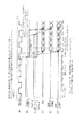
【0062】
図6および図7は、本発明の一実施例において、第1の条件により異なるメモリデバイス間またはメモリモジュール間でギャップレス・リード動作を行う場合の各々の信号波形を示すタイミングチャートのその1およびその2である。
ここでは、図6および図7のタイミングチャートを参照しながら、あるメモリデバイスまたはメモリモジュールのデータの読み出しを行った後に、他のメモリデバイスまたはメモリモジュールのデータの読み出しを連続して行う場合(ギャップレス・リード(Gapless Read)、すなわち、インタリーブ(Interleave)動作を実行する場合)の本発明の一実施例の動作を説明する。
【0063】
ただし、この場合、クロック周波数400MHzにて動作するDDR SDRAM(Double Data Rate Synchronous DRAM )からなるメモリデバイスまたはメモリモジュールが、キャス・レイテンシーCL(Column Access Strobe Signal Latency の略)=3、読み出されるデータのビット長BL=4ビット、および2Xルールの条件下で動作する場合を想定する。ここで、キャス・レイテンシーCLは、メモリデバイスが活性化された状態(アクティブ状態)のときに、CPU等によりリード命令が発行されてから何クロックサイクル目にデータ出力イネーブル信号が出力されるかを示すものである。例えば、CL=3の場合には、データ読み出し命令が発行されてから3クロックサイクル目にデータ出力イネーブル信号が出力されることになる。さらに、クロック周波数の逆数を示すクロックレートtCLK=5ns(nsは10-9秒)、データ転送速度が2.5ns、位相ずれ時間tAC=tOH≒1.25ns、システムバス長L=30cm、および、伝播遅延時間τ=3nsであると仮定する。
【0064】
さらに、ここでは、チップセットから最も近い位置にあるメモリデバイスまたはメモリモジュールのデータの読み出しを行った後に、同じ位置のメモリデバイスまたはメモリモジュールのデータの読み出しを連続して行う場合の各々の信号波形と、チップセットから最も遠い位置にあるメモリデバイスまたはメモリモジュールのデータの読み出しを行った後に、最も近い位置にあるメモリデバイスまたはメモリモジュールのデータの読み出しを連続して行う場合の各々の信号波形とを比較することとする。
【0065】
本発明の一実施例では、図6の(a)部に示すように、チップセットにより生成されたメインクロックMCLK0は、MCLKラインを介して、上記チップセットから最も遠い位置にあるメモリデバイスまたはメモリモジュールに入力される。さらに、図6の(b)部および(c)部に示すように、チップセットから最も遠い位置にあるメモリデバイスまたはメモリモジュールに入力されたメインクロックMCLKmの位相は、DLL等を用いて任意の値に調整された後に、リターンクロックRCLKmとして出力される。これと平行してリターンクロックRCLKmから派生させたデータ出力イネーブル信号(すなわち、出力活性化信号)/DQEm(または/DQEMm)が出力される(図6の(d)部)。
【0066】
メモリデバイスを対象とする場合、このデータ出力イネーブル信号/DQEmは、システムバスを介して全てのメモリデバイスに入力され、同メモリデバイス内の内部信号としてデータ出力イネーブル信号/DQEImが生成される(図6の(e)部)。さらに、リターンクロックRCLKmおよびデータ出力イネーブル信号/DQEImに同期して、チップセットからのリード命令(RDm)により選択されたメモリデバイス(すなわち、チップセットから最も遠い位置にある第mのメモリデバイス)からデータ(Q0−m〜Q3−m)が出力される(図6の(f)部)。次に、チップセットからのさらなるリード命令(RD1′)により、他のメモリデバイス、例えば、チップセットから最も近い位置にあるメモリデバイス(第1のメモリデバイス)が、ギャップレス・リード動作を実行すべき出力デバイスとして選択された場合、データ出力イネーブル信号/DQEm′(データ出力イネーブル信号/DQEmに対応する)に同期してデータ出力イネーブル信号/DQEIm′(ただし、m=1)が生成される(図7の(h)部および(i)部)。
【0067】
さらに、モノマルチバイブレータ(ワンショット)等により、選択されたメモリデバイス(第1のメモリデバイス)のデータ出力イネーブル信号/DQEIm′(ただし、m=1)を1クロック期間だけ“L”レベルにし、その他の非選択メモリデバイスのデータ出力イネーブル信号を“H”レベルにする。ここでは、選択されたメモリデバイス(第1のメモリデバイス)のみデータ出力イネーブル信号/DQEIm′にて出力回路部が活性化され、リターンクロックRCLK(RCLKm)に同期して(図7の(g)部)、以前のデータ(Q0−m〜Q3−m)の後に今回のデータ(Q0−1′〜Q3−1′)が連続して出力される(RDm−RD1モード、図7の(l)部)。この場合、リターンクロックRCLKの転送インピーダンスと、データ出力イネーブル信号/DQEおよびデータ入出力信号DQの転送インピーダンスとを一致させることにより、チップセットからは、どのメモリデバイにアクセスをかけた場合でも、リード命令発行から一定時間(ここでは、アクセス時間(アクセス・タイム)tCAC=21ns(CL×tCLK+2τ=3×5ns+2×3ns))でファーストデータを受け取ることができる。それゆえに、このファーストデータをチップセットにて受け取った後は、同チップセットは高速にてかつ途切れなくデータを受け取ることが可能になる。
【0068】
さらにまた、チップセットから最も近い位置にあるメモリデバイスのデータの読み出しを行った後に、同じ位置のメモリデバイスのデータの読み出しを連続して行う場合も、リード命令発行から一定時間(アクセス時間tCAC=21ns)でファーストデータを受け取ることができる(図7の(j)部および(k)部)。この場合、リターンクロックRCLKに同期して、以前のデータ(Q0−1〜Q3−1)の後に、同じメモリデバイス内のデータ(Q0−1′〜Q3−1′)が連続して出力されることになる(RD1−RD1′モード)。
【0069】
また一方で、メモリモジュールを対象とする場合、上記データ出力イネーブル信号/DQEMmは、システムバスを介して全てのメモリモジュール内のメモリモジュール用バッファ装置に入力され、同メモリモジュール内の複数のメモリデバイス内の内部信号としてローカルのデータ出力イネーブル信号/DQELmが生成される(図6の(e)部)。さらに、リターンクロックRCLKmおよびデータ出力イネーブル信号/DQELmに同期して、チップセットからのリード命令(RDm)により選択されたメモリモジュール、すなわち、チップセットから最も遠い位置にある第mのメモリモジュール)からデータ(Q0−m〜Q3−m)が出力される(図6の(f)部)。次に、チップセットからのさらなるリード命令(RD1′)により、他のメモリモジュール、例えば、チップセットから最も近い位置にあるメモリモジュール(第1のメモリモジュール)が、ギャップレス・リード動作を実行すべき出力モジュールとして選択された場合、データ出力イネーブル信号/DQEMm′(データ出力イネーブル信号/DQEMmに対応する)に同期してデータ出力イネーブル信号/DQELm′(ただし、m=1)が生成される(図7の(h)部および(i)部)。
【0070】
チップセットから最も近い位置にあるメモリモジュールが選択されてデータ出力イネーブル信号/DQELm′が生成された後の動作は、前述のメモリデバイスを対象とした場合の動作(図7の(j)部〜(k)部)と実質的に同じなので、ここでは、その詳細な説明を省略する。
図8および図9は、本発明の一実施例において、第2の条件により異なるメモリデバイス間またはメモリモジュール間でギャップレス・リード動作を行う場合の各々の信号波形を示すタイミングチャートのその1およびその2である。
【0071】
ここでは、前述の図6および図7の場合と同様に、あるデバイスまたはメモリモジュールのデータの読み出しを行った後に、他のメモリデバイスまたはメモリモジュールのデータの読み出しを連続して行う場合の各々の信号波形が示されている。
この場合、モノマルチバイブレータ等により、選択されたメモリデバイスまたはメモリモジュールのデータ出力イネーブル信号/DQEIm、/DQEIm′、/DQELm′または/DQELm′を1クロック期間だけ活性化する(“L”レベルにする)代わりに、データが出力されている期間中、上記のデータ出力イネーブル信号を活性化するようにしている点が、前述の図6および図7の場合と異なる(図8の(e)部、および図9の(i)部)。
【0072】
その他の条件、およびバスシステムの動作は、前述の図6および図7の場合と実質的に同じなので、ここでは、その詳細な説明を省略する。
図10および図11は、本発明の一実施例において、第3の条件により異なるメモリデバイス間でギャップレス・リード動作を行う場合の各々の信号波形を示すタイミングチャートのその1およびその2である。
【0073】
ここでは、あるメモリデバイスのデータの読み出しを行っている最中に、リード・インタラプト(Read Interrupt)動作により、他のメモリデバイスのデータの読み出しを行う場合の各々の信号波形が示されている。
この場合、チップセットからのリード命令(RDm)によって、現在データの読み出しを行っているメモリデバイス(例えば、チップセットから最も遠い位置にあるメモリデバイス)に対しバースト・ストップをかけることにより、当該メモリデバイス内部のデータ出力イネーブル信号/DQEIm′を不活性化する(図10の(e)部)。また一方で、リード・インタラプト動作(RD1′)により選択されたメモリデバイス(例えば、チップセットから最も近い位置にあるメモリデバイス)に対しバースト・スタートをかけることにより、当該メモリデバイス内部のデータ出力イネーブル信号/DQEIm′(ただし、m=1)を活性化する(図11の(i)部)。
【0074】
その他の条件、およびバスシステムの動作は、前述の図6および図7の場合と実質的に同じなので、ここでは、その詳細な説明を省略する。
図10および図11に示すようなリード・インタラプト動作による他のメモリデバイスのデータの読み出しを行う場合でも、前述の図6〜図9のギャップレス・リード動作による異なるメモリデバイス間のデータの読み出しを行う場合と同様に、チップセットからは、どのメモリデバイスにリード・インタラプト動作をかけた場合でも、リード命令発行から一定時間(ここでは、アクセス時間tCAC=21ns)でファーストデータを受け取ることができる。それゆえに、このファーストデータをチップセットにて受け取った後は、高速にてかつ途切れなくデータを受け取ることが可能になる。
【0075】
ここで、本発明の実施例を用いてデータの読み出しを行った場合のデータ転送の様子と、従来の方式を使用してデータの読み出しを行った場合のデータ転送の様子との違いをより明確にするために、従来の第2例のDQストローブ方式および従来の第3例のリターンクロック方式による各々の信号波形を図12〜図15に図示することとする。
【0076】
図12および図13は、従来のDQストローブ方式において異なるメモリデバイス間でギャップレス・リード動作を行う場合の各々の信号波形を示すタイミングチャートのその1およびその2である。
ここでは、あるメモリデバイスまたはメモリモジュールのデータの読み出しを行った後に、他のメモリデバイスまたはメモリモジュールのデータの読み出しを連続して行う場合、すなわち、インタリーブ動作を実行しようとした場合の各々の波形が示されている。ただし、この場合、クロックレートやデータ転送速度等の条件は、前述の実施例の場合と同じであると仮定する。
【0077】
従来のDQストローブ方式によるバスシステムでは、図20を参照しながら既述したように、システムバス長Lによる信号遅延時間τが生ずるために、メモリデバイスの位置により同メモリデバイスがデータ読み出し用のリード命令を受け取る時間や、メモリデバイスから出力されるDQストローブ信号DQS1〜DQSmに同期してメモリデバイスから出力されるデータをチップセットが受け取る時間がまちまちになる(図12の(a)部〜図13の(h)部)。
【0078】
それゆえに、チップセットからのリード命令(RDm)に従って所定のメモリデバイス(例えば、チップセットから最も遠い位置にあるメモリデバイス)のデータの読み出しを行ってから、他のメモリデバイス(例えば、チップセットから最も近い位置にあるメモリデバイス)に対しギャップレス・リード命令(RD1′)がかかったときに(DQストローブ信号が“H”レベルまたはハイインピーダンス状態(Hi −z)のときに)、当該メモリデバイスのチップセットからの距離がかなり異なるために、両メモリデバイスに対するアクセス時間tCACが異なってくる。この結果、図13の(k)部および(l)部に示すように、インタリーブ動作を実行しようとしても、チップセットからの距離が異なるメモリデバイス間での調停がスムーズに行えなくなる。この結果、同図のハッチング部分のようなバス衝突が発生し、高速にてデータを転送することが困難になる。なお、チップセットから最も近い位置にあるメモリデバイスのデータの読み出しを行った後に、同じ位置のメモリデバイスのデータの読み出しを連続して行う場合は、アクセス時間tCACの違いは生じないので、リード命令発行から一定時間遅延した後に、連続してデータを転送することができる(図13の(i)部および(j)部)。
【0079】
図14および図15は、従来のリターンクロック方式において異なるメモリデバイス間でギャップレス・リード動作を行う場合の各々の信号波形を示すタイミングチャートのその1およびその2である。
ここでも、あるメモリデバイスまたはメモリモジュールのデータの読み出しを行った後に、他のメモリデバイスまたはメモリモジュールのデータの読み出しを連続して行う場合、すなわち、インタリーブ動作を実行しようとした場合の各々の波形が示されている。ただし、この場合、クロックレートやデータ転送速度等の条件は、前述の実施例の場合と同じであると仮定する。
【0080】
従来のリターンクロック方式によるバスシステムでは、図21を参照しながら既述したように、システムバス長Lによる信号遅延時間τがデータ転送時間の半分以上になると、チップセットから最も近い位置にあるメモリモジュールのデータと、最も遠い位置にあるメモリモジュールのデータとのアクセス時間に差が生じてくる(図14の(a)部〜(f)部)。
【0081】
それゆえに、あるメモリデバイス(例えば、チップセットから最も遠い位置にあるメモリデバイス)のデータの読み出しを行ってから、他のメモリデバイス(例えば、チップセットから最も近い位置にあるメモリデバイス)に対しギャップレス・リード命令がかかったときに、当該メモリデバイスのチップセットからの距離がかなり異なるために、両メモリデバイスに対するアクセス時間tCACが異なってくる。この結果、図15の(g)部、(h)部および(j)部に示すように、インタリーブ動作を実行しようとしても、チップセットからの距離が異なるメモリデバイス間での調停がスムーズに行えなくなる。この結果、同図のハッチング部分のようなバス衝突が発生し、高速にてデータを転送することが困難になる。なお、チップセットから最も近い位置にあるメモリデバイスのデータの読み出しを行った後に、同じ位置のメモリデバイスのデータの読み出しを連続して行う場合は、アクセス時間tCACの違いは生じないので、リード命令発行から一定時間遅延した後に、連続してデータを転送することができる(図15の(i)部)。
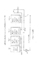
【0082】
図16は、本発明の他の実施例に係るバスシステムの構成を示すブロック図であり、図17は、本発明の他の実施例に使用されるメモリデバイスの一例を示すブロック図であり、図18は、本発明の他の実施例に使用されるメモリモジュール用バッファ装置の一例を示すブロック図である。
図16においては、図2〜図5に示した本発明の一実施例の場合と異なり、チップセット40から最も遠い位置(すなわち、第mのメモリデバイスまたはメモリモジュールが配置される位置)に、複数のメモリデバイスまたはメモリモジュール制御用のコントローラ6からなるコントローラチップを設けている。複数のメモリデバイスを制御の対象にする場合、上記コントローラ6により、リターンクロックRCLKmおよびデータ出力イネーブル信号/DQEmが生成される。あるいは、複数のメモリモジュールを制御の対象にする場合、上記コントローラ6により、リターンクロックRCLKmおよびデータ出力イネーブル信号/DQEMmが生成される。この場合、コントローラ6からなるコントローラチップに対しリターンクロックおよびデータ出力イネーブル信号を生成する機能をもたせているので、制御の対象がメモリデバイスおよびメモリモジュールのいずれであっても、上記のリターンクロックおよびデータ出力イネーブル信号をどのメモリデバイスまたはメモリモジュールから送出するかを決定するためのイネーブル端子ENは不要になる。
さらに、図16においては、システムバス7のバスラインは、データ入力時に、CPU等のチップセット(チップセット♯0)40から、−1番目のメモリデバイスまたはメモリモジュール〜第m─1のメモリデバイスまたはメモリモジュール3−1r、3−1、3−2、……、3−m─1(複数のメモリデバイスまたはメモリモジュール3−1r〜3−m─1)へ向かうメインクロックMCLKを転送するためのMCLKラインと、データ出力時に、複数のメモリモジュール3−1r〜3−m─1からチップセット40へ向かうリターンクロックRCLKを転送するためのRCLKラインとを含む。
【0083】
図16におけるコントローラ6以外の構成は、前述の図2の構成と実質的に同じなので、ここでは、その詳細な説明を省略する。
また一方で、図16においては、各々のメモリデバイスまたはメモリモジュールは、コントローラ6により生成されるリターンクロックRCLKmおよびデータ出力イネーブル信号/DQEmまたは/DQEMmを入力として受け取り、リターンクロックRCLKを生成すると共に、このリターンクロックRCLKに基づき各々のメモリデバイスの出力回路部を活性化するデータ出力イネーブル信号/DQEまたは/DQEMを生成する。このデータ出力イネーブル信号/DQEまたは/DQEMは、リターンクロックRCLKに同期し、このリターンクロックRCLKと同一方向に流れる。すなわち、データ出力イネーブル信号/DQEまたは/DQEMは、チップセット40に向って流れる。
【0084】
本発明の他の実施例にて使用される複数のメモリデバイスの各々は、好ましくは、図17に示すようなメモリデバイス31により構成される。このメモリデバイス31は、本発明のリターンクロック入出力手段(図1参照)として、チップセット40から出力されるメインクロックMCLKをもとに生成されるリターンクロックRCLKを入力するリターンクロック入力回路(図17では、第kのリターンクロック入力回路として示す)11−kを設けている。さらに、本発明の出力活性化手段(図1参照)として、上記リターンクロックRCLKをもとに生成されるデータ出力イネーブル信号/DQE(または/DQEL)を受け取り、このデータ出力イネーブル信号/DQEに基づきデータの出力を活性化する出力活性化回路(図17では、第kの出力活性化回路として示す)21−kを設けている。これらのリターンクロック入出力回路11−kおよび出力活性化回路21−kを有するメモリデバイス31の構成は、図3のメモリデバイス30の構成と基本的に同じであるが、前述のようにイネーブル端子ENが不要になっている点と、リターンクロック入力回路等の入力回路部だけで出力回路部が不要になっている点とが異なる。
【0085】
また一方で、本発明の他の実施例にて使用される複数のメモリモジュールの各々は、好ましくは、図18に示すようなメモリモジュール用バッファ装置(図18の斜線部)を有するメモリモジュール36により構成される。このメモリモジュール36は、複数のメモリデバイス31−1〜31−mと、これらの複数のメモリデバイスとチップセット40との間で、データに関連するデータ入出力信号DQやその他の信号を入出力するためのメモリモジュール用バッファ装置として機能するメモリモジュール用バッファ回路50とを備えている。
【0086】
このようなメモリモジュール36の構成は、図4のメモリモジュール35の構成と基本的に同じであるが、前述のようにイネーブル端子ENが不要になっている点が異なる。
本発明の他の実施例では、リターンクロックRCLKの発生源を示すイネーブル端子ENを設ける必要がなくなるので、前述の本発明の一実施例に比べて回路構成が簡単になる。
【0087】
【発明の効果】
以上説明したように、本発明のデータ転送メモリ装置によれば、第1に、所定の位置にあるメモリデバイスまたはメモリモジュールおよびコントローラからリターンクロックを生成すると共に、このリターンクロックに基づきデータ出力イネーブル信号を生成しているので、データ出力イネーブル信号は、リターンクロックと同一方向に流れる。このために、システムバス長がどのように長くなっても、かつ、データ転送時間が信号遅延時間の半分以下になる程高速であっても、システムバス上の任意のメモリデバイスまたはメモリモジュールから、CPU等に対し同一アクセス時間でデータを転送することができると共に、各種のデータを高速にてかつ途切れなく転送することができる。
【0088】
さらに、本発明のデータ転送メモリ装置によれば、第2に、CPU等から最も遠い位置にあるメモリデバイスまたはメモリモジュールからリターンクロックを生成すると共に、このリターンクロックに基づきデータ出力イネーブル信号を生成しているので、システムバス長による信号遅延時間変動が生じなくなり、システム全体の効率を高めることが可能になる。
【0089】
さらに、本発明のデータ転送メモリ装置によれば、第3に、CPU等から最も遠い位置にあるメモリデバイスまたはメモリモジュール以外のメモリデバイスまたはメモリモジュールは、前者のメモリデバイスまたはメモリモジュールから供給されるデータ出力イネーブル信号を入力として受け取り、当該データ出力イネーブル信号によってデータの出力を活性化すると共に、当該リターンクロックに同期してデータを出力するようにしているので、システムバス上の任意のメモリデバイスまたはメモリモジュールから、CPU等に対し同一アクセス時間でデータを転送することが可能になる。
【0090】
さらに、本発明のデータ転送装置によれば、第4に、リターンクロックおよびデータ出力イネーブル信号を任意の位相に設定することができるので、システムバス長による信号遅延が生じないようにすることが可能になる。
さらに、本発明のデータ転送装置によれば、第5に、各々のメモリデバイスまたはメモリモジュールの入力回路部が、データ出力イネーブル信号によって所定の時間のみ活性化されるようになっているので、システム全体の消費電力の節減が図れる。
【図面の簡単な説明】
【図1】本発明の原理構成を示すブロック図である。
【図2】本発明の一実施例に係るバスシステムの構成を示すブロック図である。
【図3】本発明の一実施例に使用されるメモリデバイスの一例を示す図である。
【図4】本発明の一実施例に使用されるメモリモジュール用バッファ装置の一例を示すブロック図である。
【図5】図4のメモリモジュールに使用されるメモリデバイスの一例を示すブロック図である。
【図6】本発明の一実施例において、第1の条件により異なるメモリデバイス間またはメモリモジュール間でギャップレス・リード動作を行う場合の各々の信号波形を示すタイミングチャート(その1)である。
【図7】本発明の一実施例において、第1の条件により異なるメモリデバイス間またはメモリモジュール間でギャップレス・リード動作を行う場合の各々の信号波形を示すタイミングチャート(その2)である。
【図8】本発明の一実施例において、第2の条件により異なるメモリデバイス間またはメモリモジュール間でギャップレス・リード動作を行う場合の各々の信号波形を示すタイミングチャート(その1)である。
【図9】本発明の一実施例において、第2の条件により異なるメモリデバイス間またはメモリモジュール間でギャップレス・リード動作を行う場合の各々の信号波形を示すタイミングチャート(その2)である。
【図10】本発明の一実施例において、第3の条件により異なるメモリデバイス間またはメモリモジュール間でギャップレス・リード動作を行う場合の各々の信号波形を示すタイミングチャート(その1)である。
【図11】本発明の一実施例において、第3の条件により異なるメモリデバイス間またはメモリモジュール間でギャップレス・リード動作を行う場合の各々の信号波形を示すタイミングチャート(その2)である。
【図12】従来のDQストローブ方式において異なるメモリデバイス間でギャップレス・リード動作を行う場合の各々の信号波形を示すタイミングチャート(その1)である。
【図13】従来のDQストローブ方式において異なるメモリデバイス間でギャップレス・リード動作を行う場合の各々の信号波形を示すタイミングチャート(その2)である。
【図14】従来のリターンクロック方式において異なるメモリデバイス間でギャップレス・リード動作を行う場合の各々の信号波形を示すタイミングチャート(その1)である。
【図15】従来のリターンクロック方式において異なるメモリデバイス間でギャップレス・リード動作を行う場合の各々の信号波形を示すタイミングチャート(その2)である。
【図16】本発明の他の実施例に係るバスシステムの構成を示すブロック図である。
【図17】本発明の他の実施例に使用されるメモリデバイスの一例を示すブロック図である。
【図18】本発明の他の実施例に使用されるメモリモジュール用バッファ装置の一例を示すブロック図である。
【図19】従来の第1例に係るバスシステムの構成を示すブロック図である。
【図20】従来の第2例に係るバスシステムの構成を示すブロック図である。
【図21】従来の第3例に係るバスシステムの構成を示すブロック図である。
【符号の説明】
1−1〜1−m…第1〜第mのリターンクロック入出力手段
2−1〜2−m…第1〜第mの出力活性化手段
3−1r〜3−m…−1番目〜第mのメモリデバイスまたはメモリモジュール
4…データ処理部
5…メモリモジュール用バッファ回路
6…コントローラ
7…システムバス
10−k…第kのリターンクロック入出力回路
10′−k…第kのリターンクロック入力回路
11−k…第kのリターンクロック入力回路
20−k、20′−k…第kの出力活性化回路
21−k…第kの出力活性化回路
30、30′…メモリデバイス
30−1〜30−m、30′−1〜30′−m…第1〜第mのメモリデバイス
31…メモリデバイス
31−1〜31−m…第1〜第mのメモリデバイス
35…メモリモジュール
36…メモリモジュール
40…チップセット
42…基準電圧発生回路
50…メモリモジュール用バッファ回路
120−1〜120−m…第1〜第mのメモリモジュール
500…DLL
510…バッファアンプ[0001]
BACKGROUND OF THE INVENTION
The present invention relates to a plurality of memory devices such as a plurality of DRAMs (Dimic Random Access Memory) having a function of transferring data on one system bus in a bus system, and a plurality of such memory devices each having such a memory device mounted thereon. The present invention relates to a data transfer memory device composed of a plurality of memory modules.
[0002]
In general, in a bus system, in order to increase the efficiency of the entire system, various data can be input / output between a plurality of memory devices or a plurality of memory modules and a CPU (central processing unit) at a high speed. Required.
The present invention relates to a data transfer memory device formed by arranging a plurality of memory devices on a system bus or by arranging a plurality of memory modules on which such a plurality of memory devices are mounted on the system bus. A method for transferring various data to be input / output to / from each memory device or memory module at high speed and without interruption through the bus line of the system bus will be described.
[0003]
[Prior art]
The configuration of the bus system using the conventional data transfer memory device will be described below with reference to FIGS.
FIG. 19 is a block diagram showing a configuration of a conventional bus system according to a first example. Here, the configuration of a bus system including a memory device composed of a plurality of Rambus DRAMs operating according to the Rambus method or a plurality of memory modules on which such memory devices are mounted is illustrated. However, a data transfer bus line (usually referred to as a DQ line) of the
[0004]
In FIG. 19, one chip set (chip set # 0) 40 composed of a CPU or the like, a
[0005]
Here, a transfer clock T-CLK is transferred via the data output clock line, and a receive clock R-CLK is transferred via the data input clock line. That is, in this case, by transferring the transfer clock T-CLK and the receive clock R-CLK using only the same clock line, data input to each memory device or each memory module and each memory device or The phase shift of the data output from each memory module is eliminated. The level of the signal on the clock line is adjusted by the voltage supplied from the power supply Vt via the level adjustment resistor Rt1.
[0006]
In the conventional bus system of the first example shown in FIG. 19, data output from a plurality of memory devices or memory modules to the
[0007]
On the other hand, by monitoring the time when the acknowledge packet arrives at the chip set, the chip set can know in advance the arrival of data. However, since the time for the acknowledge packet to arrive at the chipset is determined by the distance from each memory device or memory module, the chipset has to wait for that time.
[0008]
FIG. 20 is a block diagram showing a configuration of a bus system according to a second conventional example. Here, a configuration of a bus system including a plurality of memory devices that operate according to the DQ strobe method or a plurality of memory modules on which such memory devices are mounted is illustrated. Here, however, the DQ line of the
[0009]
20, the bus line of the
[0010]
Further, in FIG. 20, a chip set 40, a
In the conventional second example bus system shown in FIG. 20, a plurality of memory devices or memory modules 110-1 to 110-m receive input data in synchronization with a main clock MCLK. On the other hand, when data is output from a plurality of memory devices or memory modules (that is, when data is read), data is output in synchronization with the DQ strobe signal DQS generated by each memory device or memory module. .
[0011]
Further, the DQ strobe signal terminal is controlled from the chip set 40 even when data is input to a plurality of memory devices or memory modules (that is, when data is written), and in synchronization with the timing for controlling the DQ strobe signal terminal. There are also ways in which multiple memory devices or memory modules receive incoming data.
[0012]
In this method, since a signal delay time τ due to the system bus length L occurs, the time at which the memory device or the memory module receives a read command for reading data depending on the position of the memory device or the memory module, and the output from the memory device or the memory module. The time for receiving the data to be received by the
[0013]
In particular, the time for receiving data output from the first memory device or memory module device 110-1 located closest to the
[0014]
FIG. 21 is a block diagram showing a configuration of a conventional bus system according to a third example. Here, a configuration of a bus system including a plurality of memory modules each mounted with a plurality of memory devices that operate by a return clock method is illustrated.
In FIG. 21, the bus lines of the
[0015]
Also in FIG. 21, as in the first example of the related art shown in FIG. 19, one chip set 40 including a CPU, a
However, unlike the conventional first example shown in FIG. 19, the conventional third example bus system of FIG. 21 has a DLL (delayed delay clock) for adjusting the clock phase in each of the memory modules 120-1 to 120-m. A module buffer including a lock loop (abbreviated as “Delayed Lock Loop”) 500 and a
[0016]
In this case, according to the main clock MCLK transferred from the
[0017]
However, even in such a return clock method, when the signal delay time τ due to the system bus length L becomes more than half of the data transfer time, as in the conventional Rambus method of the first example, the closest position from the chip set 40 is obtained. There is a difference in the access time between the data of a certain memory module 120-1 and the data of the memory module 120-m located at the farthest position.
[0018]
[Problems to be solved by the invention]
As described above, in the conventional bus system of the first example, when the signal delay time caused by the bus line length of the system bus increases, the data arrives from the memory device located farthest from the chipset at the chipset. The waiting time becomes longer. For this reason, it becomes difficult to transfer data at high speed, resulting in a problem that the efficiency of the entire system is lowered.
[0019]
Furthermore, in the conventional bus system of the second example, when the signal delay time caused by the bus line length of the system bus is increased, the time for the chipset to receive the data output from the memory device or the memory module varies. For this reason, the position of the data capture window in the chipset must be changed in accordance with the relative position of the memory device or the memory module with respect to the chipset, resulting in a problem that the efficiency of the entire system is lowered.
[0020]
Furthermore, in the conventional bus system of the third example, when the signal delay time caused by the bus line length of the system bus becomes more than half of the data transfer time, as in the case of the conventional first example, the closest to the chip set. There is a difference between the time until the data of the memory module at the position reaches the chip set and the time until the data of the memory module at the farthest position reaches the chip set. For this reason, as in the case of the first conventional example, it becomes difficult to transfer data at a high speed, resulting in a problem that the efficiency of the entire system is lowered.
[0021]
The present invention has been made in view of the above problems, and transfers various data between a plurality of memory devices or a plurality of memory modules and a CPU or the like at high speed and improves the efficiency of the entire system. It is an object of the present invention to provide a data transfer memory device that can perform the above-described operation.
[0022]
[Means for Solving the Problems]
FIG. 1 is a block diagram showing the principle configuration of the present invention. Hereinafter, the same components as those described above are denoted by the same reference numerals.
As shown in FIG. 1, the data transfer memory device of the present invention has a function of transferring data on one
[0023]
In order to solve the above problem, in the data transfer apparatus of the present invention including a plurality of memory devices as shown in FIG. 1, the plurality of memory devices (first to m-th memory devices 3-1 to 3- Each of m) is a return clock input / output means (first to mth returns) for inputting / outputting a return clock RCLK generated based on a clock (for example, main clock MCLK) output from the
[0024]
Preferably, in the data transfer apparatus of the present invention including a plurality of memory devices, only the memory device at a predetermined position on the
Furthermore, preferably, in the data transfer apparatus according to the present invention including a plurality of memory devices, the memory device at the predetermined position is the memory device at the farthest position from the
[0025]
Furthermore, preferably, in the data transfer apparatus of the present invention including a plurality of memory devices, a plurality of memory devices 3-1 to 3 -m−1 other than the memory device at the predetermined position are transferred by the
[0026]
Furthermore, preferably, in the data transfer apparatus of the present invention including a plurality of memory devices, the
[0027]
Further, preferably, in the data transfer device of the present invention including a plurality of memory devices, the return clock RCLK and the data output enable signal DQE are set to arbitrary phases. Such phase adjustment of the return clock RCLK and the data output enable signal DQE is performed by a DLL or the like provided in the memory device.
[0028]
Furthermore, preferably, in the data transfer device of the present invention including a plurality of memory devices, the input circuit unit of the
On the other hand, in the data transfer device of the present invention including a plurality of memory modules as shown in FIG. 1, each of the plurality of memory modules (first to mth memory modules 3-1 to 3-m) is A plurality of memory devices, and a memory module buffer device for inputting and outputting the data and various signals between the plurality of memory devices and the
[0029]
Further, the memory module buffer device includes return clock input / output means (first to first clocks) for inputting / outputting a return clock RCLK generated based on a clock (for example, main clock MCLK) output from the
[0030]
Preferably, in the data transfer device of the present invention including a plurality of memory modules, only the memory module buffer device in the memory module at a predetermined position on the
Furthermore, preferably, in the data transfer device of the present invention including a plurality of memory modules, the memory module at the predetermined position is the memory module (at the farthest position from the
[0031]
Further preferably, in the data transfer device of the present invention including a plurality of memory modules, when the memory module buffer device other than the memory module buffer device at the predetermined position is selected for output by the
[0032]
Furthermore, preferably, in the data transfer device of the present invention including a plurality of memory modules, when a memory device in a memory module other than the memory module at the predetermined position is selected for output by the
[0033]
Further preferably, in the data transfer apparatus of the present invention including a plurality of memory modules, when the memory device mounted on the memory module at the predetermined position is selected by the
[0034]
Further preferably, in the data transfer device of the present invention including a plurality of memory modules, the return clock RCLK and the data output enable signal DQE are set to arbitrary phases. Such phase adjustment of the return clock RCLK and the data output enable signal DQE is performed by a DLL or the like provided in the memory module buffer device.
[0035]
Further preferably, in the data transfer device of the present invention including a plurality of memory modules, the input circuit unit of the
According to the data transfer apparatus of the present invention including a plurality of memory devices or a plurality of memory modules, the memory device or the memory module (for example, the mth memory device or the memory module) located farthest from the
[0036]
In particular, when a large-scale bus system such as gigabyte (GB) to terabyte (TB) is constructed, the data transfer speed in such a bus system can maintain the maximum speed. The disadvantage (penalty) when constructing such a large-scale bus system is that the first data (the
[0037]
Thus, according to the present invention, various data can be transferred between a plurality of memory devices or a plurality of memory modules and a CPU at high speed without interruption, so that the maximum data transfer speed in the bus system is maintained. In addition, the efficiency of the entire system can be increased.
[0038]
DETAILED DESCRIPTION OF THE INVENTION
Hereinafter, preferred embodiments of the present invention will be described with reference to the accompanying drawings (FIGS. 2 to 17).
2 is a block diagram showing a configuration of a bus system according to an embodiment of the present invention, FIG. 3 is a diagram showing an example of a memory device used in the embodiment of the present invention, and FIG. FIG. 5 is a block diagram showing an example of a memory module buffer device used in one embodiment of the present invention, and FIG. 5 is a block diagram showing an example of a memory device used in the memory module of FIG.
[0039]
The embodiment of the present invention shown in FIGS. 2 to 4 was basically conceived to compensate for the drawbacks of the conventional return clock system bus system (see FIG. 21) of the third example as described above. It is a bus system. Such an embodiment of the present invention can be applied not only to a memory module equipped with a plurality of memory devices but also to a memory device alone.
[0040]
In FIG. 2, the bus line of the
[0041]
Further, here, in consideration of phase shifts in the plurality of memory devices or memory modules 3-1r to 3-m, main clocks input to these memory devices or memory modules are respectively represented by MCLK-1 to MCLKm. Let's represent. Further, it is assumed that a return clock RCLKm is generated from the mth memory device or memory module 3-m located farthest from the
Furthermore, the bus line of the
[0042]
In FIG. 2, as in the third conventional example shown in FIG. 21, one chip set 40 including a CPU, a
[0043]
When a plurality of memory devices used in one embodiment of the present invention are directly connected to the
[0044]
Further, the
[0045]
Here, referring again to FIG. 2, the relationship between the input / output of the return clock RCLK and the data output enable signal / DQE in a plurality of memory devices will be described. In FIG. 2, only the enable terminal EN of the m-th memory device 3-m located farthest from the
[0046]
Further, in each of the memory devices other than the m-th memory device 3-m located farthest from the
[0047]
In this case, it should be noted that even when the memory device outputting the return clock RCLKm and the data output enable signal / DQEm is selected from the
[0048]
The same can be said for the case where the bus system is configured using a plurality of memory modules as in the case of the plurality of memory devices described above. In the plurality of memory modules used in one embodiment of the present invention, a plurality of memory devices 30'-1 to 30'-m (in FIG. 4, the first memory device 30'-1 to the first memory device) are used. m memory devices 30'-m) are connected to the
[0049]
Further, the input / output circuit portion of the memory
[0050]
Further, the
[0051]
Here, referring again to FIG. 2, the relationship between the input / output of the return clock RCLK and the data output enable signal / DQEM in the memory module buffer device in the plurality of memory modules will be described. In FIG. 2, only the enable terminal EN (ENm) of the m-th memory module located farthest from the
[0052]
Further, in FIG. 2, each of the memory module buffer devices other than the memory module buffer circuit in the m-th memory module farthest from the
[0053]
However, in the module configuration as described above, the memory module buffer circuit provided in the other memory module not only takes in the return clock RCLK and the data output enable signal / DQEM, but also in each of the memory modules. It has a function of transmitting these signals to the memory device. Therefore, the local return clock RCLKL and the data output enable signal / DQEL obtained by buffering the return clock RCLK and the data output enable signal / DQEM in the memory module are output from the memory module buffer circuit as output signals. The If necessary, after the main clock MCLK and the data input / output signal DQ are also buffered by the memory module buffer circuit, the local main clock MCLKL (L is also a local meaning) and the data input / output signal DQL (L is It is also possible to output as local meaning).
[0054]
Since the memory module used in one embodiment of the present invention is configured as described above, all of the memory devices of the module type used in this memory module are the local return clock RCLKL and data as output signals. Only an input circuit section for receiving the output enable signal / DQEL is required. Further, as a matter of course, the enable terminal EN indicating the source of the return clock and the data output enable signal is not required. One configuration example of each memory device 30 'in such a memory module is shown in FIG.
[0055]
In FIG. 5, each
[0056]
Further, in FIGS. 2, 4 and 5, each of the memory module buffer circuits other than the memory module buffer circuit located farthest from the chip set 40 is the memory module located farthest from the chip set 40. The data output enable signal / DQEMm supplied from the buffer circuit is received as an input, and is selected in the memory device in the module by the local data output enable signal / DQEL created based on the data output enable signal / DQEMm The output of the memory device data is activated, and the data is sent to the corresponding memory module buffer circuit in synchronization with the local return clock RCLKL.
[0057]
Further, in FIGS. 2, 4, and 5, each of the plurality of
[0058]
Further, in FIGS. 2, 4 and 5, each of the plurality of
[0059]
In other words, even in the module-type configuration as described above, the memory module buffer circuit (for example, the farthest from the chip set 40) in the memory module that outputs the return clock RCLK and the data output enable signal / DQEM. The memory module buffer circuit in an m-th memory module can output the return clock RCLK and the data output enable signal / DQEM to the memory module buffer circuit in the memory module. Therefore, even when the memory device in the memory module outputting the return clock RCLK and the data output enable signal / DQEM is selected from the
[0060]
The data transfer memory device used in the embodiment of the present invention shown in FIGS. 2 to 5 includes a plurality of memory devices and a plurality of memory modules including a plurality of module type memory devices. In any case, since the data output enable signal / DQE or / DQEM flows in the same direction as the return clock RCLK, any memory device on the
[0061]
Further, in the embodiment of the present invention shown in FIGS. 2 to 5, the return clock RCLK and the data output enable signal / DQE or / DQEM are provided in the memory device or the buffer circuit for the memory module in the memory module. It is possible to set an arbitrary phase by using the generated DLL.
2 to 5, the input circuit section of the chip set 40 and the input circuit section of the output activation circuit in each memory device or memory module are The data output enable signal / DQE or / DQEM is activated only for a predetermined time. Therefore, the power consumption of the chip set 40 and the output activation circuit of each memory device or memory module is reduced.
[0062]
FIGS. 6 and 7 are timing
Here, referring to the timing charts of FIGS. 6 and 7, after reading data from a certain memory device or memory module, the data from another memory device or memory module is continuously read (gapless). The operation of an embodiment of the present invention for reading (gapless read), that is, when performing an interleave operation will be described.
[0063]
In this case, however, a memory device or memory module composed of a DDR SDRAM (Double Data Rate Synchronous DRAM) operating at a clock frequency of 400 MHz has a CAS latency CL (abbreviation of Column Access Strobe Signal Latency) = 3, It is assumed that the bit length BL = 4 bits and the operation is performed under the condition of 2X rule. Here, the CAS latency CL indicates the number of clock cycles after the read command is issued by the CPU or the like when the memory device is activated (active state). It is shown. For example, when CL = 3, the data output enable signal is output at the third clock cycle after the data read command is issued. Further, a clock rate tCLK = 5 ns (ns is 10 ns) indicating the reciprocal of the clock frequency. -9 Second), the data transfer rate is 2.5 ns, the phase shift time tAC = tOH≈1.25 ns, the system bus length L = 30 cm, and the propagation delay time τ = 3 ns.
[0064]
Furthermore, here, after reading data from the memory device or memory module closest to the chipset, each signal waveform when reading data from the memory device or memory module at the same position continuously And each signal waveform when the data of the memory device or memory module located at the furthest position from the chipset is read and then the data of the memory device or memory module located at the nearest position is read continuously. Will be compared.
[0065]
In one embodiment of the present invention, as shown in part (a) of FIG. 6, the main clock MCLK0 generated by the chipset is connected to the memory device or memory farthest from the chipset via the MCLK line. Input to the module. Further, as shown in FIGS. 6B and 6C, the phase of the main clock MCLKm input to the memory device or memory module farthest from the chipset can be arbitrarily set using a DLL or the like. After being adjusted to a value, it is output as a return clock RCLKm. In parallel with this, a data output enable signal (that is, output activation signal) / DQEm (or / DQEMm) derived from the return clock RCLKm is output (part (d) of FIG. 6).
[0066]
When the memory device is targeted, the data output enable signal / DQEm is input to all the memory devices via the system bus, and the data output enable signal / DQEIm is generated as an internal signal in the memory device (see FIG. 6 (e) part). Further, in synchronization with the return clock RCLKm and the data output enable signal / DQEIm, the memory device selected by the read command (RDm) from the chipset (that is, the mth memory device farthest from the chipset) Data (Q0-m to Q3-m) is output (part (f) in FIG. 6). Next, a further read instruction (RD1 ') from the chipset causes another memory device, for example, the memory device closest to the chipset (first memory device) to perform a gapless read operation. When selected as an output device, a data output enable signal / DQEIm ′ (where m = 1) is generated in synchronization with the data output enable signal / DQEm ′ (corresponding to the data output enable signal / DQEm) (FIG. 5). 7 (h) part and (i) part).
[0067]
Furthermore, the data output enable signal / DQEIm ′ (where m = 1) of the selected memory device (first memory device) is set to the “L” level for one clock period by a mono multivibrator (one-shot) or the like, Data output enable signals of other non-selected memory devices are set to “H” level. Here, only the selected memory device (first memory device) activates the output circuit section by the data output enable signal / DQEIm ′ and synchronizes with the return clock RCLK (RCLKm) ((g) of FIG. 7). Part), the previous data (Q0-m to Q3-m) and the current data (Q0-1 'to Q3-1') are continuously output (RDm-RD1 mode, (l) in FIG. 7). Part). In this case, by making the transfer impedance of the return clock RCLK coincide with the transfer impedance of the data output enable signal / DQE and the data input / output signal DQ, the chip set can read any memory device. Fast data can be received at a fixed time (in this case, access time (access time) tCAC = 21 ns (CL × tCLK + 2τ = 3 × 5 ns + 2 × 3 ns)). Therefore, after receiving the first data in the chip set, the chip set can receive the data at high speed and without interruption.
[0068]
Furthermore, when data is read from the memory device closest to the chipset and then continuously read from the memory device at the same position, a certain time (access time tCAC = 21 ns), the first data can be received (part (j) and part (k) in FIG. 7). In this case, data (Q0-1 ′ to Q3-1 ′) in the same memory device is continuously output after the previous data (Q0-1 to Q3-1) in synchronization with the return clock RCLK. (RD1-RD1 ′ mode).
[0069]
On the other hand, when the memory module is targeted, the data output enable signal / DQEMm is input to the memory module buffer device in all the memory modules via the system bus, and a plurality of memory devices in the memory module are input. A local data output enable signal / DQELm is generated as an internal signal (part (e) of FIG. 6). Further, in synchronization with the return clock RCLKm and the data output enable signal / DQELm, from the memory module selected by the read command (RDm) from the chipset, that is, the mth memory module farthest from the chipset) Data (Q0-m to Q3-m) is output (part (f) in FIG. 6). Next, according to a further read command (RD1 ′) from the chipset, another memory module, for example, the memory module closest to the chipset (first memory module) should perform a gapless read operation. When selected as an output module, a data output enable signal / DQELm ′ (where m = 1) is generated in synchronization with the data output enable signal / DQEMm ′ (corresponding to the data output enable signal / DQEMm) (FIG. 1). 7 (h) part and (i) part).
[0070]
The operation after the memory module closest to the chip set is selected and the data output enable signal / DQELm ′ is generated is the operation when the above-described memory device is targeted (part (j) in FIG. 7 to (K) part) is substantially the same, and detailed description thereof is omitted here.
FIGS. 8 and 9 are timing
[0071]
Here, as in the case of FIG. 6 and FIG. 7 described above, after reading data from a certain device or memory module, each data reading from another memory device or memory module is continuously performed. The signal waveform is shown.
In this case, the data output enable signal / DQEIm, / DQEIm ′, / DQELm ′ or / DQELm ′ of the selected memory device or memory module is activated for one clock period by the mono multivibrator or the like (set to “L” level). Instead, the above-described data output enable signal is activated during the period in which the data is output, which is different from the case of FIG. 6 and FIG. 7 (part (e) of FIG. 8). And (i) part of FIG. 9).
[0072]
Since the other conditions and the operation of the bus system are substantially the same as those in FIGS. 6 and 7, the detailed description thereof will be omitted here.
FIGS. 10 and 11 are timing
[0073]
Here, each signal waveform when data of another memory device is read by a read interrupt operation while data of a certain memory device is being read is shown.
In this case, in response to a read command (RDm) from the chipset, a memory device that is currently reading data (for example, a memory device located farthest from the chipset) is subjected to a burst stop, whereby the memory The data output enable signal / DQEIm ′ in the device is inactivated (part (e) of FIG. 10). On the other hand, by performing a burst start on the memory device (for example, the memory device closest to the chipset) selected by the read interrupt operation (RD1 ′), the data output enable inside the memory device is enabled. The signal / DQEIm ′ (where m = 1) is activated (part (i) in FIG. 11).
[0074]
Since the other conditions and the operation of the bus system are substantially the same as those in FIGS. 6 and 7, the detailed description thereof will be omitted here.
Even when data of another memory device is read by the read interrupt operation as shown in FIGS. 10 and 11, data is read between different memory devices by the gapless read operation of FIGS. As is the case with any memory device from the chipset. The Even when a read interrupt operation is performed, the first data can be received within a fixed time (in this case, the access time tCAC = 21 ns) after the read command is issued. Therefore, after receiving the first data by the chip set, it becomes possible to receive the data at high speed and without interruption.
[0075]
Here, the difference between the state of data transfer when data is read using the embodiment of the present invention and the state of data transfer when data is read using the conventional method is more clearly shown. In order to achieve this, the respective signal waveforms according to the DQ strobe method of the second conventional example and the return clock method of the third conventional example are shown in FIGS.
[0076]
12 and 13 are timing
Here, each waveform when reading data from another memory device or memory module continuously after reading data from another memory device or memory module, that is, when attempting to perform an interleave operation It is shown. However, in this case, it is assumed that conditions such as a clock rate and a data transfer rate are the same as those in the above-described embodiment.
[0077]
In the conventional bus system using the DQ strobe method, as already described with reference to FIG. 20, since the signal delay time τ due to the system bus length L is generated, the memory device reads the data for reading data depending on the position of the memory device. The time for receiving an instruction and the time for receiving data output from the memory device in synchronization with the DQ strobe signals DQS1 to DQSm output from the memory device vary (part (a) in FIG. 12 to FIG. 13). (H) part).
[0078]
Therefore, after reading data from a predetermined memory device (for example, the memory device farthest from the chipset) in accordance with a read command (RDm) from the chipset, other memory devices (for example, from the chipset) When a gapless read command (RD1 ') is applied to the nearest memory device (when the DQ strobe signal is at "H" level or high impedance state (Hi-z)), the memory device Because the distance from the chipset is quite different, the access time tCAC for both memory devices will be different. As a result, as shown in the (k) part and (l) part of FIG. 13, even if an interleave operation is attempted, arbitration between memory devices having different distances from the chipset cannot be performed smoothly. As a result, a bus collision such as the hatched portion in the figure occurs, making it difficult to transfer data at high speed. Note that when data is read continuously from the memory device located closest to the chipset and then continuously read out from the memory device at the same position, there is no difference in the access time tCAC. Data can be transferred continuously after a certain time delay from issuance (part (i) and part (j) in FIG. 13).
[0079]
FIGS. 14 and 15 are timing
Again, each waveform when reading data from one memory device or memory module and then continuously reading data from another memory device or memory module, that is, when trying to perform an interleave operation It is shown. However, in this case, it is assumed that conditions such as a clock rate and a data transfer rate are the same as those in the above-described embodiment.
[0080]
In the conventional bus system based on the return clock system, as already described with reference to FIG. 21, when the signal delay time τ due to the system bus length L becomes more than half of the data transfer time, the memory closest to the chipset is located. There is a difference in the access time between the module data and the data of the farthest memory module (parts (a) to (f) in FIG. 14).
[0081]
Therefore, after reading data from one memory device (for example, the memory device farthest from the chipset), it is gapless with respect to another memory device (for example, the memory device closest to the chipset). When the read command is issued, the access time tCAC for the two memory devices differs because the distance from the chip set of the memory device is considerably different. As a result, as shown in (g) part, (h) part, and (j) part of FIG. 15, even when trying to perform the interleave operation, arbitration can be smoothly performed between memory devices having different distances from the chipset. Disappear. As a result, a bus collision such as the hatched portion in the figure occurs, making it difficult to transfer data at high speed. Note that when data is read continuously from the memory device located closest to the chipset and then continuously read out from the memory device at the same position, there is no difference in the access time tCAC. Data can be transferred continuously after a certain time delay from issuance (part (i) in FIG. 15).
[0082]
FIG. 16 is a block diagram showing a configuration of a bus system according to another embodiment of the present invention, and FIG. 17 is a block diagram showing an example of a memory device used in another embodiment of the present invention. FIG. 18 is a block diagram showing an example of a memory module buffer device used in another embodiment of the present invention.
In FIG. 16, unlike the embodiment of the present invention shown in FIGS. 2 to 5, the farthest position from the chipset 40 (that is, the position where the mth memory device or memory module is disposed) A controller chip including a plurality of memory devices or a controller 6 for controlling a memory module is provided. When a plurality of memory devices are to be controlled, the controller 6 generates a return clock RCLKm and a data output enable signal / DQEm. Alternatively, when a plurality of memory modules are to be controlled, the controller 6 generates a return clock RCLKm and a data output enable signal / DQEMm. In this case, since the controller chip comprising the controller 6 has a function of generating a return clock and a data output enable signal, the above-described return clock and data are controlled regardless of whether the control target is a memory device or a memory module. The enable terminal EN for determining which memory device or memory module the output enable signal is sent from becomes unnecessary.
Further, in FIG. 16, the bus line of the
[0083]
Since the configuration other than the controller 6 in FIG. 16 is substantially the same as the configuration in FIG. 2, the detailed description thereof is omitted here.
On the other hand, in FIG. 16, each memory device or memory module receives the return clock RCLKm and the data output enable signal / DQEm or / DQEMm generated by the controller 6 as inputs, generates the return clock RCLK, Based on the return clock RCLK, a data output enable signal / DQE or / DQEM for activating the output circuit portion of each memory device is generated. The data output enable signal / DQE or / DQEM flows in the same direction as the return clock RCLK in synchronization with the return clock RCLK. That is, the data output enable signal / DQE or / DQEM flows toward the chip set 40.
[0084]
Each of the plurality of memory devices used in another embodiment of the present invention is preferably constituted by a
[0085]
On the other hand, each of the plurality of memory modules used in another embodiment of the present invention preferably has a memory module buffer device (shaded portion in FIG. 18) as shown in FIG. Consists of. The
[0086]
The configuration of such a
In another embodiment of the present invention, it is not necessary to provide an enable terminal EN indicating the source of the return clock RCLK, so that the circuit configuration is simplified compared to the above-described embodiment of the present invention.
[0087]
【The invention's effect】
As described above, according to the data transfer memory device of the present invention, first, the return clock is generated from the memory device or the memory module and the controller at the predetermined position, and the data output enable signal is generated based on the return clock. Therefore, the data output enable signal flows in the same direction as the return clock. For this reason, from any memory device or memory module on the system bus, no matter how long the system bus length increases and the data transfer time is as fast as half the signal delay time, Data can be transferred to the CPU or the like in the same access time, and various data can be transferred at high speed without interruption.
[0088]
Furthermore, according to the data transfer memory device of the present invention, second, a return clock is generated from a memory device or a memory module located farthest from the CPU or the like, and a data output enable signal is generated based on the return clock. Therefore, the signal delay time fluctuation due to the system bus length does not occur, and the efficiency of the entire system can be improved.
[0089]
Further, according to the data transfer memory device of the present invention, thirdly, the memory device or memory module other than the memory device or memory module farthest from the CPU or the like is supplied from the former memory device or memory module. Since the data output enable signal is received as an input and the data output is activated by the data output enable signal and the data is output in synchronization with the return clock, any memory device on the system bus or Data can be transferred from the memory module to the CPU or the like in the same access time.
[0090]
Furthermore, according to the data transfer device of the present invention, fourthly, the return clock and the data output enable signal can be set to arbitrary phases, so that signal delay due to the system bus length can be prevented. become.
Furthermore, according to the data transfer apparatus of the present invention, fifthly, the input circuit portion of each memory device or memory module is activated only for a predetermined time by the data output enable signal. The overall power consumption can be reduced.
[Brief description of the drawings]
FIG. 1 is a block diagram showing a principle configuration of the present invention.
FIG. 2 is a block diagram showing a configuration of a bus system according to an embodiment of the present invention.
FIG. 3 is a diagram showing an example of a memory device used in an embodiment of the present invention.
FIG. 4 is a block diagram showing an example of a memory module buffer device used in an embodiment of the present invention.
5 is a block diagram showing an example of a memory device used in the memory module of FIG.
FIG. 6 is a timing chart (No. 1) showing signal waveforms when a gapless read operation is performed between different memory devices or memory modules according to the first condition in the embodiment of the present invention.
FIG. 7 is a timing chart (No. 2) showing respective signal waveforms when a gapless read operation is performed between different memory devices or memory modules according to the first condition in the embodiment of the present invention.
FIG. 8 is a timing chart (part 1) showing signal waveforms when a gapless read operation is performed between different memory devices or memory modules according to a second condition in the embodiment of the present invention.
FIG. 9 is a timing chart (No. 2) showing signal waveforms when a gapless read operation is performed between different memory devices or memory modules according to a second condition in the embodiment of the present invention.
FIG. 10 is a timing chart (part 1) showing signal waveforms when a gapless read operation is performed between different memory devices or memory modules according to a third condition in the embodiment of the present invention.
FIG. 11 is a timing chart (part 2) showing signal waveforms when a gapless read operation is performed between different memory devices or memory modules according to a third condition in the embodiment of the present invention.
FIG. 12 is a timing chart (No. 1) showing signal waveforms when a gapless read operation is performed between different memory devices in the conventional DQ strobe method.
FIG. 13 is a timing chart (No. 2) showing signal waveforms when a gapless read operation is performed between different memory devices in the conventional DQ strobe method.
FIG. 14 is a timing chart (No. 1) showing signal waveforms when a gapless read operation is performed between different memory devices in the conventional return clock method.
FIG. 15 is a timing chart (No. 2) showing signal waveforms when a gapless read operation is performed between different memory devices in the conventional return clock method.
FIG. 16 is a block diagram showing a configuration of a bus system according to another embodiment of the present invention.
FIG. 17 is a block diagram showing an example of a memory device used in another embodiment of the present invention.
FIG. 18 is a block diagram showing an example of a memory module buffer device used in another embodiment of the present invention.
FIG. 19 is a block diagram showing a configuration of a bus system according to a first conventional example.
FIG. 20 is a block diagram showing a configuration of a bus system according to a second conventional example.
FIG. 21 is a block diagram showing a configuration of a bus system according to a third conventional example.
[Explanation of symbols]
1-1 to 1-m ... 1st to m-th return clock input / output means
2-1 to 2-m ... 1st to mth output activation means
3-1r to 3-m ...- 1st to m-th memory device or memory module
4. Data processing unit
5 ... Buffer circuit for memory module
6 ... Controller
7 ... System bus
10-k: k-th return clock input / output circuit
10'-k ... kth return clock input circuit
11-k: k-th return clock input circuit
20-k, 20'-k ... k-th output activation circuit
21-k: k-th output activation circuit
30, 30 '... Memory device
30-1 to 30-m, 30'-1 to 30'-m ... 1st to m-th memory devices
31 ... Memory device
31-1 to 31-m... 1st to mth memory devices
35 ... Memory module
36 ... Memory module
40 ... Chipset
42. Reference voltage generation circuit
50. Buffer circuit for memory module
120-1 to 120-m ... 1st to m-th memory modules
500 ... DLL
510 ... Buffer amplifier
Claims (11)
前記データ処理部から出力されるクロックをもとに生成されるリターンクロックを入出力するリターンクロック入出力手段と、
該リターンクロック入出力手段から出力されるリターンクロックをもとに生成されるデータ出力イネーブル信号に基づき、前記データの出力を活性化する出力活性化手段とを備え、
前記システムバス上で前記データ処理部から最も遠い位置にあるメモリデバイスのみが、前記リターンクロックおよび前記データ出力イネーブル信号を生成するように構成され、
前記データ処理部から最も遠い位置にあるメモリデバイス以外の前記メモリデバイスが、前記データ処理部により出力選択された場合、前記データ処理部から最も遠い位置にあるメモリデバイスにて生成される前記リターンクロックおよび前記データ出力イネーブル信号を入力として受け取り、当該データ出力イネーブル信号によって前記データの出力を活性化すると共に、当該リターンクロックに同期して該データを出力することが可能であることを特徴とするデータ転送メモリ装置。In a data transfer memory device having a function of transferring data on a single system bus and including a plurality of memory devices controlled by a data processing unit that processes the data, each of the plurality of memory devices includes:
Return clock input / output means for inputting / outputting a return clock generated based on the clock output from the data processing unit;
Output activation means for activating the output of the data based on a data output enable signal generated based on a return clock output from the return clock input / output means;
Only the memory device located farthest from the data processing unit on the system bus is configured to generate the return clock and the data output enable signal,
When the memory device other than the memory device farthest from the data processing unit is selected for output by the data processing unit, the return clock generated by the memory device farthest from the data processing unit And receiving the data output enable signal as an input, activating the output of the data by the data output enable signal, and outputting the data in synchronization with the return clock Transfer memory device.
該複数のメモリモジュールの各々は、複数のメモリデバイスと、該複数のメモリデバイスと前記データ処理部との間で前記データおよび各種の信号を入出力するためのメモリモジュール用バッファ装置とを備えており、
各々の前記メモリモジュール内の該メモリモジュール用バッファ装置は、
前記データ処理部から出力されるクロックをもとに生成されるリターンクロックを入出力するリターンクロック入出力手段と、
該リターンクロック入出力手段から出力されるリターンクロックをもとに生成されるデータ出力イネーブル信号に基づき、前記複数のメモリデバイスからの前記データの出力を活性化する出力活性化手段とを備え、
前記システムバス上において、前記データ処理部から最も遠い位置にあるメモリモジュール内のメモリモジュール用バッファ装置以外の前記メモリモジュール用バッファ装置が、前記データ処理部により出力選択された場合、前記データ処理部から最も遠い位置にあるメモリモジュール内のメモリモジュール用バッファ装置にて生成される前記リターンクロックおよび前記データ出力イネーブル信号を入力として受け取り、前記の出力選択されたメモリモジュール内の前記メモリデバイスに供給することを特徴とするデータ転送メモリ装置。In a data transfer memory device having a function of transferring data on one system bus and including a plurality of memory modules controlled by a data processing unit for processing the data,
Each of the plurality of memory modules includes a plurality of memory devices, and a memory module buffer device for inputting and outputting the data and various signals between the plurality of memory devices and the data processing unit. And
The memory module buffer device in each of the memory modules includes:
Return clock input / output means for inputting / outputting a return clock generated based on the clock output from the data processing unit;
Output activation means for activating output of the data from the plurality of memory devices based on a data output enable signal generated based on a return clock output from the return clock input / output means;
When the memory module buffer device other than the memory module buffer device in the memory module located farthest from the data processing unit on the system bus is selected for output by the data processing unit, the data processing unit The return clock and the data output enable signal generated by the memory module buffer device in the memory module farthest from the memory module are received as inputs and supplied to the memory device in the memory module selected for output. A data transfer memory device.
前記の出力選択されたメモリモジュール内の前記メモリデバイスは、当該メモリモジュール用バッファ装置から供給される当該データ出力イネーブル信号を入力として受け取り、当該データ出力イネーブル信号によって前記データの出力を活性化すると共に、当該リターンクロックに同期して、対応するメモリモジュール用バッファ装置に該データを送出する請求項6記載のデータ転送メモリ装置。When the output of the memory module buffer device other than the memory module buffer device in the memory module farthest from the data processing unit is selected by the data processing unit, the memory module buffer device is at the farthest position from the data processing unit. Receiving the return clock and the data output enable signal generated by the memory module buffer device in the memory module as inputs, and supplying them to the memory device in the memory module selected for output;
The memory device in the output-selected memory module receives the data output enable signal supplied from the memory module buffer device as an input, and activates the output of the data by the data output enable signal. 7. The data transfer memory device according to claim 6, wherein the data is sent to the corresponding memory module buffer device in synchronization with the return clock.
Priority Applications (4)
| Application Number | Priority Date | Filing Date | Title |
|---|---|---|---|
| JP31392797A JP3832947B2 (en) | 1997-11-14 | 1997-11-14 | Data transfer memory device |
| US09/129,424 US6393541B1 (en) | 1997-11-14 | 1998-08-05 | Data transfer memory having the function of transferring data on a system bus |
| KR1019980035092A KR100281952B1 (en) | 1997-11-14 | 1998-08-28 | Data transfer memory device |
| US10/122,179 US6708263B2 (en) | 1997-11-14 | 2002-04-16 | Data transfer memory having the function of transferring data on a system bus |
Applications Claiming Priority (1)
| Application Number | Priority Date | Filing Date | Title |
|---|---|---|---|
| JP31392797A JP3832947B2 (en) | 1997-11-14 | 1997-11-14 | Data transfer memory device |
Publications (2)
| Publication Number | Publication Date |
|---|---|
| JPH11149437A JPH11149437A (en) | 1999-06-02 |
| JP3832947B2 true JP3832947B2 (en) | 2006-10-11 |
Family
ID=18047200
Family Applications (1)
| Application Number | Title | Priority Date | Filing Date |
|---|---|---|---|
| JP31392797A Expired - Fee Related JP3832947B2 (en) | 1997-11-14 | 1997-11-14 | Data transfer memory device |
Country Status (3)
| Country | Link |
|---|---|
| US (2) | US6393541B1 (en) |
| JP (1) | JP3832947B2 (en) |
| KR (1) | KR100281952B1 (en) |
Families Citing this family (19)
| Publication number | Priority date | Publication date | Assignee | Title |
|---|---|---|---|---|
| JP3832947B2 (en) * | 1997-11-14 | 2006-10-11 | 富士通株式会社 | Data transfer memory device |
| JP2001035188A (en) * | 1999-07-26 | 2001-02-09 | Fujitsu Ltd | Test method for semiconductor device and semiconductor device |
| TW482954B (en) * | 2000-11-10 | 2002-04-11 | Via Tech Inc | Internal operation method of chip set to reduce the power consumption |
| US7313715B2 (en) | 2001-02-09 | 2007-12-25 | Samsung Electronics Co., Ltd. | Memory system having stub bus configuration |
| US6445624B1 (en) * | 2001-02-23 | 2002-09-03 | Micron Technology, Inc. | Method of synchronizing read timing in a high speed memory system |
| KR100391990B1 (en) * | 2001-06-14 | 2003-07-22 | 삼성전자주식회사 | Information processing system with memory modules of a serial bus architecture |
| JP4308461B2 (en) * | 2001-10-05 | 2009-08-05 | ラムバス・インコーポレーテッド | Semiconductor memory device |
| US6963991B2 (en) * | 2002-05-31 | 2005-11-08 | Intel Corporation | Synchronizing and aligning differing clock domains |
| DE60210170T2 (en) * | 2002-07-15 | 2006-11-02 | Infineon Technologies Ag | storage system |
| KR100520219B1 (en) * | 2003-01-03 | 2005-10-11 | 삼성전자주식회사 | memory module device for use in high frequency operation |
| US7436010B2 (en) * | 2003-02-13 | 2008-10-14 | Matsushita Electric Industrial Co., Ltd. | Solid state imaging apparatus, method for driving the same and camera using the same |
| US7234099B2 (en) * | 2003-04-14 | 2007-06-19 | International Business Machines Corporation | High reliability memory module with a fault tolerant address and command bus |
| US8214541B2 (en) * | 2006-06-07 | 2012-07-03 | Dell Products L.P. | Method and system for uniquely identifying peripheral component devices |
| US20080086590A1 (en) * | 2006-10-04 | 2008-04-10 | Masayuki Urabe | Flash Memory Control Interface |
| KR101373793B1 (en) * | 2006-10-04 | 2014-03-13 | 마벨 월드 트레이드 리미티드 | Flash memory control interface |
| US20090091963A1 (en) * | 2007-10-04 | 2009-04-09 | Advanced Micro Devices, Inc. | Memory device |
| JP5025785B2 (en) * | 2010-12-17 | 2012-09-12 | 株式会社東芝 | Semiconductor memory device |
| KR101977664B1 (en) | 2012-09-14 | 2019-05-13 | 삼성전자주식회사 | EMBEDDED MULTIMEDIA CARD(eMMC), AND HOST FOR CONTROLLING THE eMMC |
| US10803000B2 (en) * | 2017-12-04 | 2020-10-13 | Synopsys, Inc. | Phase-aware control and scheduling |
Family Cites Families (3)
| Publication number | Priority date | Publication date | Assignee | Title |
|---|---|---|---|---|
| US4980850A (en) * | 1987-05-14 | 1990-12-25 | Digital Equipment Corporation | Automatic sizing memory system with multiplexed configuration signals at memory modules |
| US5243703A (en) | 1990-04-18 | 1993-09-07 | Rambus, Inc. | Apparatus for synchronously generating clock signals in a data processing system |
| JP3832947B2 (en) * | 1997-11-14 | 2006-10-11 | 富士通株式会社 | Data transfer memory device |
-
1997
- 1997-11-14 JP JP31392797A patent/JP3832947B2/en not_active Expired - Fee Related
-
1998
- 1998-08-05 US US09/129,424 patent/US6393541B1/en not_active Expired - Lifetime
- 1998-08-28 KR KR1019980035092A patent/KR100281952B1/en not_active IP Right Cessation
-
2002
- 2002-04-16 US US10/122,179 patent/US6708263B2/en not_active Expired - Lifetime
Also Published As
| Publication number | Publication date |
|---|---|
| US20020112136A1 (en) | 2002-08-15 |
| KR100281952B1 (en) | 2001-03-02 |
| US6393541B1 (en) | 2002-05-21 |
| US6708263B2 (en) | 2004-03-16 |
| KR19990044805A (en) | 1999-06-25 |
| JPH11149437A (en) | 1999-06-02 |
Similar Documents
| Publication | Publication Date | Title |
|---|---|---|
| JP3832947B2 (en) | Data transfer memory device | |
| US6847583B2 (en) | Method of synchronizing read timing in a high speed memory system | |
| KR100822001B1 (en) | Semiconductor memory device and operating method of semiconductor memory circuit | |
| US6851016B2 (en) | System latency levelization for read data | |
| JP4070051B2 (en) | Data masking method and circuit for semiconductor memory device, and semiconductor memory device having the circuit | |
| US20010054135A1 (en) | Memory control technique | |
| KR102435438B1 (en) | Apparatus and method comprising memory instructions for semiconductor memory | |
| JP2817679B2 (en) | Semiconductor memory | |
| US6052329A (en) | Output circuit and synchronous semiconductor memory device having a function of preventing output of invalid data | |
| JP4308461B2 (en) | Semiconductor memory device | |
| JP2002132580A (en) | Semiconductor memory device and memory system | |
| JP2010192031A (en) | Semiconductor memory device, memory module including the same, and data processing system | |
| JPH09204769A (en) | Semiconductor memory device and memory system using it | |
| JP2002025261A (en) | Method and circuit for inputting-outputting data and system for adopting semiconductor memory device provided with the same | |
| KR102327983B1 (en) | Apparatus and method comprising memory instructions for semiconductor memory | |
| JP4495381B2 (en) | Semiconductor memory device | |
| KR100933257B1 (en) | Semiconductor memory device | |
| JPH10283779A (en) | Synchronous type semiconductor storage device | |
| JP2003283322A (en) | Interface circuit and semiconductor device | |
| JPH1021684A (en) | Synchronous semiconductor memory device | |
| US6504767B1 (en) | Double data rate memory device having output data path with different number of latches |
Legal Events
| Date | Code | Title | Description |
|---|---|---|---|
| A977 | Report on retrieval |
Free format text: JAPANESE INTERMEDIATE CODE: A971007 Effective date: 20060322 |
|
| A131 | Notification of reasons for refusal |
Free format text: JAPANESE INTERMEDIATE CODE: A131 Effective date: 20060328 |
|
| A521 | Written amendment |
Free format text: JAPANESE INTERMEDIATE CODE: A523 Effective date: 20060529 |
|
| TRDD | Decision of grant or rejection written | ||
| A01 | Written decision to grant a patent or to grant a registration (utility model) |
Free format text: JAPANESE INTERMEDIATE CODE: A01 Effective date: 20060620 |
|
| A61 | First payment of annual fees (during grant procedure) |
Free format text: JAPANESE INTERMEDIATE CODE: A61 Effective date: 20060718 |
|
| R150 | Certificate of patent or registration of utility model |
Free format text: JAPANESE INTERMEDIATE CODE: R150 |
|
| S111 | Request for change of ownership or part of ownership |
Free format text: JAPANESE INTERMEDIATE CODE: R313111 |
|
| FPAY | Renewal fee payment (event date is renewal date of database) |
Free format text: PAYMENT UNTIL: 20090728 Year of fee payment: 3 |
|
| R350 | Written notification of registration of transfer |
Free format text: JAPANESE INTERMEDIATE CODE: R350 |
|
| FPAY | Renewal fee payment (event date is renewal date of database) |
Free format text: PAYMENT UNTIL: 20100728 Year of fee payment: 4 |
|
| FPAY | Renewal fee payment (event date is renewal date of database) |
Free format text: PAYMENT UNTIL: 20100728 Year of fee payment: 4 |
|
| FPAY | Renewal fee payment (event date is renewal date of database) |
Free format text: PAYMENT UNTIL: 20110728 Year of fee payment: 5 |
|
| FPAY | Renewal fee payment (event date is renewal date of database) |
Free format text: PAYMENT UNTIL: 20110728 Year of fee payment: 5 |
|
| S531 | Written request for registration of change of domicile |
Free format text: JAPANESE INTERMEDIATE CODE: R313531 |
|
| S533 | Written request for registration of change of name |
Free format text: JAPANESE INTERMEDIATE CODE: R313533 |
|
| FPAY | Renewal fee payment (event date is renewal date of database) |
Free format text: PAYMENT UNTIL: 20110728 Year of fee payment: 5 |
|
| R371 | Transfer withdrawn |
Free format text: JAPANESE INTERMEDIATE CODE: R371 |
|
| S531 | Written request for registration of change of domicile |
Free format text: JAPANESE INTERMEDIATE CODE: R313531 |
|
| S533 | Written request for registration of change of name |
Free format text: JAPANESE INTERMEDIATE CODE: R313533 |
|
| FPAY | Renewal fee payment (event date is renewal date of database) |
Free format text: PAYMENT UNTIL: 20110728 Year of fee payment: 5 |
|
| R350 | Written notification of registration of transfer |
Free format text: JAPANESE INTERMEDIATE CODE: R350 |
|
| FPAY | Renewal fee payment (event date is renewal date of database) |
Free format text: PAYMENT UNTIL: 20120728 Year of fee payment: 6 |
|
| FPAY | Renewal fee payment (event date is renewal date of database) |
Free format text: PAYMENT UNTIL: 20120728 Year of fee payment: 6 |
|
| FPAY | Renewal fee payment (event date is renewal date of database) |
Free format text: PAYMENT UNTIL: 20130728 Year of fee payment: 7 |
|
| S531 | Written request for registration of change of domicile |
Free format text: JAPANESE INTERMEDIATE CODE: R313531 |
|
| R350 | Written notification of registration of transfer |
Free format text: JAPANESE INTERMEDIATE CODE: R350 |
|
| LAPS | Cancellation because of no payment of annual fees |