JP3825908B2 - Image forming apparatus - Google Patents
Image forming apparatus Download PDFInfo
- Publication number
- JP3825908B2 JP3825908B2 JP7353398A JP7353398A JP3825908B2 JP 3825908 B2 JP3825908 B2 JP 3825908B2 JP 7353398 A JP7353398 A JP 7353398A JP 7353398 A JP7353398 A JP 7353398A JP 3825908 B2 JP3825908 B2 JP 3825908B2
- Authority
- JP
- Japan
- Prior art keywords
- transfer
- image
- developer
- particles
- forming apparatus
- Prior art date
- Legal status (The legal status is an assumption and is not a legal conclusion. Google has not performed a legal analysis and makes no representation as to the accuracy of the status listed.)
- Expired - Fee Related
Links
Images


Landscapes
- Cleaning In Electrography (AREA)
- Electrostatic Charge, Transfer And Separation In Electrography (AREA)
- Developing Agents For Electrophotography (AREA)
Description
【0001】
【発明の属する技術分野】
本発明は、電子写真感光体や静電記録誘電体等の像担持体に適宜の潜像形成プロセスにて形成した潜像を粉体現像剤(以下、トナーと記す)で現像し、その現像剤像(以下、トナー画像と記す)を記録媒体(以下、転写材と記す)に転写させて画像形成を実行する転写方式の画像形成装置に関する。
【0002】
【従来の技術】
従来、上記のような転写方式の画像形成装置において、像担持体に形成担持させたトナー画像を転写材に転写する手段としては、コロナ帯電器を用いたコロナ転写装置や、導電性ローラーを用いたローラー転写装置が使用されている。
【0003】
コロナ転写装置は、像担持体に対してコロナ帯電器をその放電開口部を対向させて非接触に配設し、その像担持体とコロナ帯電器の間に転写材を通紙し、該転写材の裏面をコロナ帯電器から放出させた、トナーの帯電極性とは逆極性のコロナシャワーにさらすことで帯電させて像担持体側のトナー画像を転写材の表面側に静電転写させるものである。
【0004】
ローラー転写装置は、導電性ローラー(以下、転写ローラーと記す)を像担持体に接触させて配設して転写ニップ部を形成させ、その転写ニップ部に転写材を導入して挟持搬送させ、転写ローラーにはトナーの帯電極性とは逆極性の転写バイアス電圧を印加することで像担持体側のトナー画像を転写材の表面側に静電転写させるものである。
【0005】
【発明が解決しようとする課題】
A)しかしながら、いずれの転写装置においても像担持体側から転写材側へのトナー画像の転写が100%行なわれることはなく、転写材へのトナー画像転写後の像担持体には転写残トナーが存在する。
【0006】
そこで一般には転写部の次位にクリーニング装置(クリーナー)を配設具備させ、該クリーニング装置により転写後の像担持体上の転写残トナーを除去させ、像担持体を繰り返して作像に供するようにしている。像担持体上から除去されてクリーニング装置に溜る転写残トナーは廃トナーとなる。そのような廃トナーは経済性やエコロジー等の観点から量的に少ないか、実質的にでないことが望ましい。
【0007】
B)クリーニング装置をなしにし、転写後の像担持体上の転写残トナーは現像装置によって「現像同時クリーニング」で像担持体上から除去し現像装置に回収・再用する装置構成にしたクリーナーレスシステム(トナーリサイクルプロセス)の画像形成装置も出現している。
【0008】
現像同時クリーニングとは、転写後に像担持体上に残留したトナーを次工程以降の現像時、即ち引き続き感光体を帯電し、露光して潜像を形成し、該潜像の現像時にかぶり取りバイアス(現像装置に印加する直流電圧と像担持体の表面電位間の電位差であるかぶり取り電位差Vback)によって回収する方法である。この方法によれば、転写残トナーは現像装置に回収されて次工程以後に再用されるため、廃トナーをなくし、メンテナンスに手を煩わせることも少なくすることができる。またクリーナーレスであることでスペース面での利点も大きく、画像形成装置を大幅に小型化できるようになる。
【0009】
しかし、このようなクリーナーレス系の画像形成装置の場合でも、転写部から現像部に至る間に像担持体に接触して作用する部材がある場合、例えば帯電ローラー等の接触帯電部材がある場合には、そのような接触部材に転写残トナーが付着・混入することになり、転写残トナーが量的に多ければ接触部材のトナーによる汚染の度合いも大きくなり、画像形成に悪影響することになる。また転写残トナーが量的に多ければ現像同時クリーニングも負担となる。
【0010】
したがって、上記A)のクリーニング装置を有する転写方式画像形成装置の場合も、B)のクリーナーレス系の転写方式画像形成装置の場合も、転写性の向上が課題となっている。
【0011】
そこで本発明は転写方式画像形成装置において転写性の可及的向上を図ることを目的とする。
【0012】
【課題を解決するための手段】
本発明は下記の構成を特徴とする画像形成装置である。
【0013】
(1)像担持体に潜像を形成するプロセス手段に、像担持体とニップ部を形成し像担持体面を帯電する可撓性の帯電手段を有し、像担持体に形成した潜像を粉体現像剤で現像し、その現像剤像を記録媒体に転写させて画像形成を実行する転写方式の画像形成装置において、前記帯電手段が、粒径が粉体現像剤の径の1/50以上1/2以下で、導電性の粒子を像担持体上にコートする手段を兼ねており、像担持体上に該粒子がコートされた状態において、潜像の形成、該潜像の粉体現像剤による現像、該現像剤像の記録媒体への転写がなされることを特徴とする画像形成装置。
(2)像担持体に形成した潜像を粉体現像剤で現像する現像手段と、像担持体上の現像剤像を記録媒体へ転写する転写手段を有する画像形成装置において、前記現像手段が現像剤像を記録媒体に転写した後に像担持体上に残留した現像剤を回収するクリーニング手段を兼ねており、前記転写手段が像担持体に対する接触転写部材であり、該接触転写部材が、粒径が粉体現像剤の径の1/50以上1/2以下で、導電性の粒子を像担持体上にコートする手段を兼ねており、像担持体上に該粒子がコートされた状態において、潜像の形成、該潜像の粉体現像剤による現像、該現像剤像の記録媒体への転写がなされることを特徴とする画像形成装置。
【0014】
(3)前記(1)または(2)に記載の画像形成装置において、前記粒子の抵抗値が1×10¹²(Ω/cm)以下であることを特徴とする画像形成装置。
【0015】
(4)前記(1)または(2)に記載の画像形成装置において、前記粒子の抵抗値が1×10¹⁰(Ω/cm)以下であることを特徴とする画像形成装置。
【0019】
〈作 用〉
a)粒径が粉体現像剤(トナー)の径の1/50以上1/2以下であり、抵抗値が1×1012(Ω/cm)以下の粒子(以下、転写促進粒子と記す)を像担持体上にコートした状態において、潜像の形成、該潜像のトナー現像をすることで、トナー画像は実質的に転写促進粒子がコートされた像担持体上に形成担持され、像担持体表面と直接に接触するトナーが減少することにより、トナーと像担持体表面間の付着力が減少し、離型性が向上する。そのため従来のように像担持体表面に直接にトナー画像を形成担持させた場合よりもトナー画像の転写性を向上させることが出来る。
【0020】
b)トナー画像は上記のように転写部において像担持体側から転写材側に効率良く移行して転写されるが、転写促進粒子はその抵抗値を1×10¹²(Ω/cm)以下のものにすることで、像担持体側から転写材側に転写されににく、クリーナーレスシステムの画像形成装置にあっては像担持体表面にコートの転写促進粒子が減少することが防止され、少量の転写促進粒子であっても長期にわたって安定に像担持体表面をコートした状態にすることが可能になり、安定した効果を上げることが可能である。
【0021】
c)また転写促進粒子の粒径は、良好な転写性を得るために、現像剤(トナー)の径の1/50以上1/2以下が望ましいことが後述の実施形態例に示すようわかった。
【0022】
【発明の実施の形態】
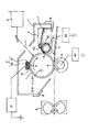
〈実施形態例1〉(図1・図2)
図1は本発明に従う画像形成装置の一例の概略構成模型図である。
【0023】
本例の画像形成装置は、転写式電子写真プロセス利用、接触帯電方式、クリーナーレスシステム、プロセスカートリッシ着脱式のレーザー・ビーム・プリンター(記録装置)である。
【0024】
(1)本例プリンタの全体的な概略構成
1は像担持体としての、φ30mmの回転ドラム型のOPC感光体(ネガ感光体)であり、矢印の時計方向に94mm/secの周速度(プロセススピード)をもって回転駆動される。
【0025】
2は感光体1に接触させて配設した接触帯電部材としての可撓性部材である固定ファーブラシである。nは該固定ファーブラシ2と感光体1とのニップ部である帯電部である。
【0026】
本例の固定ファーブラシ2は、レイヨンとカーボンからなる中抵抗の繊維(ファー)21を基布22に折込パイル状に形成したものを用いた。感光体周方向の長さは15mmであり、基布22は感光体1の周方向に沿うように円弧形に固定した。本例で用いたファー21の密度は1平方インチ当たり10万本である。
【0027】
この固定ファーブラシ2に帯電バイアス印加電源S1から、感光体1の外周面がほぼ−700Vに一様に帯電処理されるように帯電バイアス電圧が印加される。
【0028】
本例においてはこの固定ファーブラシ2に感光体1面に対して転写促進粒子(転写補助粒子)をコートする手段を兼ねさせてある。即ち、固定ファーブラシ2に転写促進粒子mを分散させて含ませてあり、この固定ファーブラシ2により転写促進粒子mが感光体1面に対して均一にコートされる。転写促進粒子mについては後述する。
【0029】
3はレーザーダイオード・ポリゴンミラー等を含むレーザービームスキャナ(露光器)である。このレーザービームスキャナは目的の画像情報の時系列電気ディジタル画素信号に対応して強度変調されたレーザー光を出力し、該レーザー光で上記回転感光体1の一様帯電面を走査露光Lする。この走査露光Lにより回転感光体1の面に目的の画像情報に対応した静電潜像が形成される。
【0030】
4は現像装置である。回転感光体1面の静電潜像はこの現像装置によりトナー画像として現像される。
【0031】
本例の現像装置4は、現像剤として負帯電性の平均粒径7μmの磁性1成分絶縁現像剤(ネガトナー)tを用いた、非接触型の反転現像装置である。
【0032】
41はマグネットロール42を内包させた、現像剤担持搬送部材として直径16mmの非磁性現像スリーブである。この現像スリーブ41は感光体1に対して500μmの離間距離をあけて対向配設し、感光体1との対向部である現像部(現像領域部)aにて感光体1の回転方向と順方向に感光体1と等速で回転させた。この回転現像スリーブ41に弾性ブレード43で現像剤が薄層にコートされる。現像剤は弾性ブレード43で回転現像スリーブ41に対する層厚が規制され、また電荷が付与される。回転現像スリーブ41にコートされた現像剤はスリーブ41の回転により、感光体1とスリーブ41の対向部である現像部aに搬送される。またスリーブ41には現像バイアス印加電源S2より現像バイアス電圧が印加される。現像バイアス電圧は、−500VのDC電圧と、周波数1800Hz、ピーク間電圧1600Vの矩形のAC電圧を重畳したものを用い、現像スリーブ4aと感光体1の間で1成分ジャンピング現像を行なわせた。
【0033】
5は接触転写手段としての中抵抗の転写ローラーであり、感光体1に所定に圧接させて転写ニップ部bを形成させてある。この転写ニップ部bに不図示の給紙部から所定のタイミングで記録媒体としての転写材Pが給紙され、かつ転写ローラー5に転写バイアス印加電源S3から所定の転写バイアス電圧が印加されることで、感光体1側のトナー像が転写ニップ部bに給紙された転写材Pの面に順次に転写されていく。本例ではローラー抵抗値は5×10⁸Ωのものを用い、+2000VのDC電圧を印加して転写を行なった。即ち、転写ニップ部bに導入された転写材Pはこの転写ニップ部bを挟持搬送されて、その表面側に回転感光体1の表面に形成担持されているトナー画像が順次に静電気力と押圧力にて転写されていく。
【0034】
6は熱定着方式等の定着装置である。転写ニップ部bに給紙されて感光体1側のトナー像の転写を受けた転写材Pは回転感光体1の面から分離されてこの定着装置6に導入され、トナー像の定着を受けて画像形成物(プリント、コピー)ととして装置外へ排出される。
【0035】
本例のプリンタはクリーナーレスであり、転写材Pに対するトナー像転写後の回転感光体1面に残留の転写残トナーはクリーナーで除去されることなく、感光体1の回転にともない帯電部nを経由して現像部aに至り、現像装置4において現像同時クリーニング(回収)される(トナーリサイクルプロセス)。
【0036】
現像同時クリーニングは前述したように、転写後に感光体1上に残留したトナーを引き続く画像形成工程の現像時、即ち引き続き感光体を帯電し、露光して潜像を形成し、その潜像の現像時において、現像装置のかぶり取りバイアス、即ち現像装置に印加する直流電圧と感光体の表面電位間の電位差であるかぶり取り電位差Vback によって回収するものである。本実施例におけるプリンタのように反転現像の場合では、この現像同時クリーニングは、感光体の暗部電位から現像スリーブにトナーを回収する電界と、現像スリーブから感光体の明部電位へトナーを付着させる電界の作用でなされる。
【0037】
7はプリンタ本体に対して着脱自在のプロセスカートリッジである。本例のプリンタは、感光体1、帯電ローラ2、現像装置6の3つのプロセス機器を一括してプリンタ本体に対して着脱自在のプロセスカートリッジとして構成してある。プロセスカートリッジ化するプロセス機器の組み合わせ等は上記に限られるものではなく任意である。8・8はプロセスカートリジの着脱案内・保持部材である。
【0038】
(2)転写促進粒子m
本例において転写促進粒子mは、比抵抗が107 Ω・cm、平均粒径1.5μmの導電性酸化亜鉛粒子を用いた。これを固定ファーブラシ2中に4g分散させた。
【0039】
回転感光体1の外周面は、この固定ファーブラシ2により所定の極性・電位に一様に接触帯電処理されるとともに、転写促進粒子mの一様なコート処理を受ける。そして回転感光体1はその外面に転写促進粒子mがコートされた状態において、レーザー走査露光Lによる潜像の形成、該潜像の現像装置4によるトナー現像を受けることで、トナー画像は実質的に転写促進粒子がコートされた感光体1上に形成担持され、感光体1の表面と直接に接触するトナーが減少することにより、トナーと感光体表面間の付着力が減少し、離型性が向上する。そのため従来のように感光体表面に直接にトナー画像を形成担持させた場合よりもトナー画像の転写性を向上させることが出来る。
【0040】
トナー画像は転写部bにおいて感光体1側から転写材P側に効率良く移行して転写されるが、転写促進粒子はその抵抗値を1×10¹²(Ω/cm)以下、より好ましくは1×1010(Ω/cm)以下のものにすることで、感光体1側から転写材P側に転写されにくく、本例のようにクリーナーレスシステムの画像形成装置にあっては感光体表面に一旦コートした転写促進粒子が減少することが防止され、少量の転写促進粒子であっても長期にわたって安定に像担持体表面をコートした状態に保たせることが可能になり、安定した効果を上げることが可能である。
【0041】
また転写促進粒子の粒径は、良好な転写性を得るために、現像剤(トナー)の径の1/50以上1/2以下が望ましい。
【0042】
転写促進粒子mは本例では比抵抗が1×10⁷ Ω・cm、二次凝集体を含めた平均粒径1.5μmの導電性酸化亜鉛粒子を用いたけれども、帯電促進粒子mの材料としては、他の金属酸化物などの導電性無機粒子や有機物との混合物など各種導電粒子が使用可能である。抵抗値が1×10¹²Ω・cm以下であれば、感光体1にコートした転写促進粒子が転写部bにおいて転写材Pに転写されにくく、効果を生じる。
【0043】
抵抗測定は、錠剤法により測定し正規化して求めた。即ち、底面積2.26cm2 の円筒内に凡そ0.5gの粉体試料を入れ上下電極に15kgの加圧を行うと同時に100Vの電圧を印加し抵抗値を計測、その後正規化して比抵抗を算出した。
【0044】
本発明において、粒子が凝集体として構成されている場合の粒径は、その凝集体としての平均粒径として定義した。粒径の測定には、光学あるいは電子顕微鏡による観察から、100個以上抽出し、水平方向最大弦長をもって体積粒度分布を算出し、その50%平均粒径をもって決定した。
【0045】
転写促進粒子mは画像露光時に妨げにならないよう、無色あるいは白色の粒子が適切である。さらに、カラー記録を行なう場合、転写促進粒子mが感光体1上から転写材Pに転写した場合を考えると無色、あるいは白色に近いものが望ましい。
【0046】
また、粒子mは露光の妨げにならないように非磁性であることが好ましい。
【0047】
以上述べたように転写促進粒子mは、一次粒子の状態で存在するばかりでなく二次粒子の凝集した状態で存在することもなんら問題はない。どのような凝集状態であれ、凝集体として転写促進粒子としての機能が実現できればその形態は重要ではない。
【0048】
像担持体としての感光体1の面に対する転写促進粒子のコート量は実際上で、100個/mm2 〜100000個/mm2 が適当であった。100個/mm2 より少ないと十分な転写効率の向上が得られず、100000個/mm2 より多過ぎると画質の低下など作像上に悪影響がでる。
【0049】
(3)転写性の評価
以上のような画像形成装置、および使用した転写促進粒子mの粒径、抵抗値が異なる画像形成装置を用いて転写性評価を行い、比較を行った。
【0050】
転写性の測定は、ベタ黒印字時(現像後の感光体1表面の現像剤量は0.15mg/cm2 )の転写前後の感光体1表面上に付着している現像剤の量を測定し、次式により転写効率を求めた。また、測定はベタ黒を印字開始直後および100枚後の2回行った。
【0051】
転写効率=(転写前現像剤量−転写後現像剤量)/転写前現像剤量
使用した転写促進粒子の粒径、抵抗値、およびその場合の転写効率を表1に示す。
【0052】
【表1】

【0053】
しかし条件を満足しない粒子Dおよび粒子Eでは良好な転写効率が得られなかった。また、粒子Bでは初期には転写性が良好であったが、粒子の抵抗値が高いために転写材P上に転写され、粒子が感光体表面から減少してしまい、100枚後には転写性が悪化した。
【0054】
以上の結果を粒子の抵抗値と粒径の図にしたものを図2に示す。図2に表されているように、本例は転写促進粒子の粒径が現像剤(トナー)の径の1/50以上1/2以下であることによって良好な転写性が得られ、抵抗値が1×1012Ω・cm以下であることによって良好な転写性を維持することが出来た。
【0055】
〈参考例〉(図3)
クリーナーレスシステムの画像形成装置において現像手段を像担持体に対する転写促進粒子コート手段として兼用させることもできる。図3はその例である。
【0056】
本例の画像形成装置は、前述実施形態例1(図1)のクリーナーレスシステムの画像形成装置において、接触帯電手段としての固定ファーブラシ2を導電性弾性ローラー2A(帯電ローラー)に変更し、また現像装置4の現像剤(トナー)tに転写促進粒子mを添加混入した。本例では現像剤t100重量部に対して転写促進粒子mを1重量部添加混入した。前記したように像担持体としての感光体1の面に対する転写促進粒子のコート量が、100個/mm2 〜100000 個/mm2 になるように現像剤tに対する転写促進粒子mの配合量を設定するもので、一般に現像剤t100重量部に対して転写促進粒子mは0.01〜20 重量部である。
【0057】
本例では転写促進粒子mを現像剤tに添加することにより、感光体1表面に転写促進粒子mを安定してコートし、転写促進粒子mの比抵抗を107 Ω・cmにすることによって感光体1表面から転写促進粒子が減少するのを防ぎ、転写性を向上させている。
【0058】
帯電ローラー2Aは、芯金2a上にゴムあるいは発泡体の中抵抗層2bを形成することにより作成される。中抵抗層2bは樹脂(例えばウレタン)、導電性粒子(例えばカーボンブラック)、硫化剤、発泡剤等により処方され、芯金2a上にローラー状に形成した。その後、表面を研磨した。帯電ローラー2は感光体1に従動回転させるか、感光体1と周速差をもたせて感光体に順方向あるいは逆方向に回転駆動される。
【0059】
画像形成装置の構成としては、感光体の帯電を帯電ローラー2Aで行い、転写促進粒子mが現像剤tに添加されていることを除けば、実施形態例1のクリーナーレスシステムの画像形成装置とほぼ同じである。
【0060】
現像剤tは公知の結着樹脂、磁性体粒子、電荷制御剤を混合し、混練、粉砕、分級の各行程を経て作成し、更に前述の転写促進粒子mを外添剤として添加し作成されたものである。
【0061】
ここで、現像剤tの重量平均粒径は7μmであり、これに対し転写促進粒子mとしての導電性酸化亜鉛粒子の粒径は1.5μmである。
【0062】
本例では、現像装置4により転写促進粒子mを安定して感光体1表面にコートすることができ、また転写促進粒子mが低抵抗であることにより、転写されず、そのため感光体1表面に安定してコートされるため、良好な転写性を得ることが出来る。
【0063】
〈実施形態例2〉(図4)
クリーナーレスシステムの画像形成装置において、接触転写部材を像担持体に対する転写促進粒子コート手段として兼用させることもできる。図4はその例である。
【0064】
本例の画像形成装置は、前述実施形態例1(図1)のクリーナーレスシステムの画像形成装置において、接触帯電手段としての固定ファーブラシ2を導電性弾性ローラー2A(帯電ローラー)に変更し、また転写ローラー5に転写促進粒子mを供給することにより、安定して感光体1表面に転写促進粒子mをコートすることを特徴とする。
【0065】
転写ローラー5への転写促進粒子mの供給は、転写ローラー5を転写促進粒子容器9内に収容させ、その容器9中で転写ローラー5に転写促進粒子mをコートする。その後に、該転写ローラー5を介して転写促進粒子mが感光体1表面に付着する。
【0066】
このため、転写促進粒子mにより転写性を向上させつつ、転写ローラー5に現像剤が付着しづらいため、良好な転写性を得ることが出来る。
【0067】
本例では、転写ローラー5に転写促進粒子mを供給することにより、感光体1表面に転写促進粒子mをコートするために、転写性を向上させつつ、転写ローラー5が現像剤により汚染されることを防ぎ、良好な転写性を得ることが出来る。
【0068】
〈その他〉
1)実施形態例2において帯電手段はコロナ帯電器であってもよい。実施形態例1において転写手段はコロナ転写装置であってもよい。
【0069】
2)実施形態例1はクリーナーレスシステムの画像形成装置であるが、クリーニング装置を有する画像形成装置であってもよい。この場合は像担持体にコートした転写促進粒子はクリーニング装置で除去されて消費されるけれども、像担持体に対する転写促進粒子のコートによる本発明の転写効率の向上効果は享受できる。
【0070】
3)実施形態例では現像装置4は、磁性の現像剤を用いた1成分非接触型現像装置であるが、2成分現像剤や、非磁性の現像剤を用いる非接触型あるいは接触型現像装置でも構わない。
【0071】
4)接触帯電部材2・2Aや現像スリーブ41に対する印加帯電バイアスあるいは印加現像バイアスは直流電圧に交番電圧(交流電圧)を重畳してもよい。
【0072】
交番電圧の波形としては、正弦波、矩形波、三角波等適宜使用可能である。また、直流電源を周期的にオン/オフすることによって形成された矩形波であっても良い。このように交番電圧の波形としては周期的にその電圧値が変化するようなバイアスが使用できる。
【0073】
5)静電潜像形成のための画像露光手段としては、実施形態例の様にデジタル的な潜像を形成するレーザー走査露光手段に限定されるものではなく、通常のアナログ的な画像露光やLEDなどの他の発光素子でも構わないし、蛍光燈等の発光素子と液晶シャッター等の組み合わせによるものなど、画像情報に対応した静電潜像を形成できるものであるなら構わない。
【0074】
感光体1は静電記録誘電体等であっても良い。この場合は、該誘電体面を所定の極性・電位に一様に一次帯電した後、除電針ヘッド、電子銃等の除電手段で選択的に除電して目的の静電潜像を書き込み形成する。
【0075】
6)感光体1からトナー画像の転写を受ける記録媒体は転写ドラム等の中間転写体であってもよい。
【0076】
7)トナー粒度の測定方法の1例を述べる。測定装置とては、コールターカウンターTA−2型(コールター社製)を用い、個数平均分布、体積平均分布を出力するインターフェイス(日科機製)及びCX−1パーソナルコンピュータ(キヤノン製)を接続し、電解液は一級塩化ナトリウムを用いて1%NaCl水溶液を調整する。
【0077】
測定法としては、前記電解水溶液100〜150ml中に分散剤として界面活性剤、好ましくは、アルキルベンゼンスルホン酸塩0.1〜5ml加え、更に測定試料を0.5〜50mg加える。
【0078】
試料を懸濁した電解液は、超音波分散器で訳1〜3分間分散処理を行ない、前記コールターカウンターTA−2型により、アパーチャーとして100μmアパーチャーを用いて2〜40μmの粒子の粒度分布を測定して、体積平均分布を求める。これらの求めた体積平均分布より体積平均粒径を得る。
【0079】
【発明の効果】
以上説明したように本発明によれば、転写方式画像形成装置において転写性の可及的向上を図ることができて、クリーニング装置を有する転写方式画像形成装置にあっては廃トナー量を少なくして経済性やエコロジーの観点から有効であり、クリーナーレス系の転写方式画像形成装置の場合も、転写部から現像部に至る間に像担持体に接触して作用する部材がある場合、例えば帯電ローラー等の接触帯電部材がある場合でも、そのような接触部材に転写残トナーが多く付着・混入することによる悪影響をなくするあるいは緩和することができる。
【図面の簡単な説明】
【図1】 実施形態例1における画像形成装置の概略構成図
【図2】 転写促進粒子の粒径と抵抗値の相関図
【図3】 参考例における画像形成装置の概略構成図
【図4】 実施形態例2における画像形成装置の概略構成図
【符号の説明】
1 感光体(像担持体)
2・2A 接触帯電部材(ファーブラシ、ローラー)
3 レーザービームスキャナ(露光器)
4 現像装置
41 現像スリーブ
t 現像剤(トナー)
m 転写促進粒子
5 転写ローラー
6 定着装置
7 プロセスカートリッジ
P 転写材[0001]
BACKGROUND OF THE INVENTION
In the present invention, a latent image formed by an appropriate latent image forming process on an image carrier such as an electrophotographic photosensitive member or an electrostatic recording dielectric is developed with a powder developer (hereinafter referred to as toner), and the development is performed. The present invention relates to a transfer type image forming apparatus that performs image formation by transferring an agent image (hereinafter referred to as a toner image) onto a recording medium (hereinafter referred to as a transfer material).
[0002]
[Prior art]
Conventionally, in a transfer-type image forming apparatus as described above, a corona transfer device using a corona charger or a conductive roller is used as a means for transferring a toner image formed and supported on an image carrier to a transfer material. The roller transfer device that was used is used.
[0003]
In the corona transfer device, a corona charger is disposed in a non-contact manner with the discharge opening facing the image carrier, and a transfer material is passed between the image carrier and the corona charger to transfer the transfer material. The back surface of the material is discharged from a corona charger, and is charged by exposing it to a corona shower having a polarity opposite to the charging polarity of the toner, so that the toner image on the image carrier side is electrostatically transferred to the surface side of the transfer material. .
[0004]
The roller transfer device is arranged by bringing a conductive roller (hereinafter referred to as a transfer roller) into contact with the image carrier to form a transfer nip portion, introducing a transfer material into the transfer nip portion, and nipping and conveying the transfer material. By applying a transfer bias voltage having a polarity opposite to the charging polarity of the toner to the transfer roller, the toner image on the image carrier side is electrostatically transferred to the surface side of the transfer material.
[0005]
[Problems to be solved by the invention]
A) However, in any of the transfer apparatuses, the transfer of the toner image from the image carrier side to the transfer material side is not 100%, and transfer residual toner is not transferred to the image carrier after the toner image is transferred to the transfer material. Exists.
[0006]
Therefore, in general, a cleaning device (cleaner) is disposed next to the transfer portion, and the transfer residual toner on the image carrier after transfer is removed by the cleaning device, and the image carrier is repeatedly used for image formation. I have to. The transfer residual toner removed from the image carrier and collected in the cleaning device becomes waste toner. It is desirable that such waste toner is small in quantity or not substantially from the viewpoint of economy and ecology.
[0007]
B) Cleanerless without a cleaning device, and the transfer residual toner on the image carrier after transfer is removed from the image carrier by “development simultaneous cleaning” by the developing device, and is collected and reused in the developing device. An image forming apparatus of a system (toner recycling process) has also appeared.
[0008]
Simultaneous development cleaning means that toner remaining on the image carrier after transfer is developed in the subsequent process, that is, the photosensitive member is continuously charged and exposed to form a latent image, and a fog removal bias is applied when the latent image is developed. (A fog removal potential difference Vback which is a potential difference between the DC voltage applied to the developing device and the surface potential of the image carrier). According to this method, since the transfer residual toner is collected by the developing device and reused after the next step, waste toner can be eliminated, and troublesome maintenance can be reduced. Further, the cleaner-less has a great space advantage, and the image forming apparatus can be greatly downsized.
[0009]
However, even in the case of such a cleaner-less image forming apparatus, when there is a member that acts in contact with the image carrier between the transfer unit and the developing unit, for example, there is a contact charging member such as a charging roller. In this case, the transfer residual toner adheres to and is mixed in such a contact member. If the amount of transfer residual toner is large, the degree of contamination of the contact member with the toner increases, which adversely affects image formation. . Further, if there is a large amount of residual toner, simultaneous development cleaning becomes a burden.
[0010]
Therefore, in both the transfer type image forming apparatus having the cleaning device A) and the cleaner-less transfer type image forming apparatus B), improvement in transferability is a problem.
[0011]
Accordingly, an object of the present invention is to improve transferability as much as possible in a transfer type image forming apparatus.
[0012]
[Means for Solving the Problems]
The present invention is an image forming apparatus having the following configuration.
[0013]
(1) The process means for forming a latent image on the image carrier has flexible charging means for forming a nip portion with the image carrier and charging the surface of the image carrier, and the latent image formed on the image carrier is In a transfer-type image forming apparatus that develops with a powder developer and transfers the developer image to a recording medium to execute image formation, the charging means has a particle size that is 1/50 of the diameter of the powder developer. Above 1/2 or less, also serves as means for coating conductive particles on the image carrier, and in the state where the particles are coated on the image carrier, formation of a latent image, powder of the latent image An image forming apparatus, wherein development with a developer and transfer of the developer image onto a recording medium are performed.
(2) In an image forming apparatus having a developing unit that develops a latent image formed on an image carrier with a powder developer, and a transfer unit that transfers a developer image on the image carrier to a recording medium. It also serves as a cleaning means for recovering the developer remaining on the image carrier after the developer image is transferred to the recording medium, and the transfer means is a contact transfer member for the image carrier, and the contact transfer member is a particle transfer member. The diameter is also 1/50 or more and 1/2 or less of the diameter of the powder developer, and also serves as a means for coating conductive particles on the image carrier. In a state where the particles are coated on the image carrier. An image forming apparatus comprising: forming a latent image; developing the latent image with a powder developer; and transferring the developer image to a recording medium.
[0014]
(3) The image forming apparatus according to (1) or (2) , wherein the particle has a resistance value of 1 × 10 12 (Ω / cm) or less.
[0015]
(4) The image forming apparatus according to (1) or (2) , wherein the particle has a resistance value of 1 × 10 10 (Ω / cm) or less.
[0019]
<Operation>
a) Particles having a particle diameter of 1/50 or more and 1/2 or less of the diameter of the powder developer (toner) and having a resistance value of 1 × 10 12 (Ω / cm) or less (hereinafter referred to as transfer promoting particles) The toner image is formed and supported on the image carrier coated with the transfer accelerating particles by forming a latent image and developing the toner on the latent image in a state where the image carrier is coated on the image carrier. By reducing the amount of toner that is in direct contact with the surface of the carrier, the adhesion between the toner and the surface of the image carrier is reduced, and the releasability is improved. Therefore, the transferability of the toner image can be improved as compared with the conventional case where the toner image is directly formed and supported on the surface of the image carrier.
[0020]
b) As described above, the toner image is efficiently transferred from the image carrier side to the transfer material side at the transfer portion as described above, but the transfer promoting particles have a resistance value of 1 × 10 12 (Ω / cm) or less. This makes it difficult to transfer from the image carrier side to the transfer material side, and in the image forming apparatus of the cleanerless system, it is prevented that the transfer promoting particles of the coat are reduced on the surface of the image carrier. Even with the transfer accelerating particles, the surface of the image carrier can be stably coated over a long period of time, and a stable effect can be improved.
[0021]
c) Further, it was found that the particle size of the transfer accelerating particle is preferably 1/50 or more and 1/2 or less of the diameter of the developer (toner) in order to obtain good transferability, as shown in the exemplary embodiments described later. .
[0022]
DETAILED DESCRIPTION OF THE INVENTION
<
FIG. 1 is a schematic configuration diagram of an example of an image forming apparatus according to the present invention.
[0023]
The image forming apparatus of this example is a transfer-type electrophotographic process use, a contact charging system, a cleanerless system, and a process cartridge removable laser beam printer (recording apparatus).
[0024]
(1) The overall
[0025]
[0026]
As the fixed
[0027]
A charging bias voltage is applied to the fixed
[0028]
In this example, the fixed
[0029]
A laser beam scanner (exposure device) 3 includes a laser diode, a polygon mirror, and the like. This laser beam scanner outputs a laser beam whose intensity is modulated in accordance with the time-series electric digital pixel signal of the target image information, and scans and exposes the uniformly charged surface of the
[0030]
[0031]
The developing
[0032]
[0033]
[0034]
[0035]
The printer of this example is cleaner-less, and residual transfer residual toner remaining on the surface of the rotating
[0036]
As described above, the simultaneous development cleaning is performed in the image forming process in which the toner remaining on the
[0037]
[0038]
(2) Transfer accelerating particles m
In this example, conductive zinc oxide particles having a specific resistance of 10 7 Ω · cm and an average particle size of 1.5 μm were used as the transfer promoting particles m. 4 g of this was dispersed in the fixed
[0039]
The outer peripheral surface of the
[0040]
The toner image is efficiently transferred from the
[0041]
The particle size of the transfer accelerating particles is preferably 1/50 to 1/2 of the diameter of the developer (toner) in order to obtain good transferability.
[0042]
In this example, the transfer promoting particle m is a conductive zinc oxide particle having a specific resistance of 1 × 10 7 Ω · cm and an average particle size of 1.5 μm including secondary aggregates. Various conductive particles such as conductive inorganic particles such as other metal oxides and mixtures with organic substances can be used. When the resistance value is 1 × 10 12 Ω · cm or less, the transfer accelerating particles coated on the
[0043]
The resistance was measured by the tablet method and normalized. That is, a powder sample of about 0.5 g is put in a cylinder with a bottom area of 2.26 cm 2, a pressure of 15 kg is applied to the upper and lower electrodes, a voltage of 100 V is applied and a resistance value is measured, and then normalized to obtain a specific resistance Was calculated.
[0044]
In the present invention, the particle size when the particles are constituted as an aggregate is defined as an average particle size as the aggregate. For the measurement of the particle size, 100 or more samples were extracted from observation with an optical or electron microscope, the volume particle size distribution was calculated with the maximum horizontal chord length, and the 50% average particle size was determined.
[0045]
The transfer accelerating particles m are suitably colorless or white particles so as not to interfere with image exposure. Further, when performing color recording, considering the case where the transfer accelerating particles m are transferred from the
[0046]
The particles m are preferably non-magnetic so as not to interfere with exposure.
[0047]
As described above, there is no problem that the transfer accelerating particles m exist not only in the state of primary particles but also in the state of aggregation of secondary particles. In any aggregation state, the form is not important as long as the function as the transfer promoting particle can be realized as an aggregate.
[0048]
In practice, the coating amount of the transfer accelerating particles on the surface of the
[0049]
(3) Evaluation of transferability Transferability was evaluated and compared using the image forming apparatus as described above, and image forming apparatuses in which the transfer promoting particles m used had different particle diameters and resistance values.
[0050]
The transferability is measured by measuring the amount of developer adhering to the surface of the
[0051]
Transfer efficiency = (pre-transfer developer amount−post-transfer developer amount) / transfer pre-transfer particle size, resistance value, and transfer efficiency in that case are shown in Table 1.
[0052]
[Table 1]
[0053]
However, good transfer efficiency could not be obtained with particles D and E that did not satisfy the conditions. In addition, the transferability of the particles B was good at the initial stage, but because of the high resistance value of the particles, the particles were transferred onto the transfer material P, and the particles decreased from the surface of the photoconductor. Worsened.
[0054]
FIG. 2 shows a graph of the resistance values and particle sizes of the above results. As shown in FIG. 2, in this example, good transferability is obtained when the particle size of the transfer accelerating particles is 1/50 or more and 1/2 or less of the diameter of the developer (toner). Was 1 × 10 12 Ω · cm or less, it was possible to maintain good transferability.
[0055]
<Reference example> (Fig. 3)
In the image forming apparatus of the cleanerless system, the developing means can be used also as the transfer accelerating particle coating means for the image carrier. FIG. 3 shows an example.
[0056]
The image forming apparatus of this example is the image forming apparatus of the cleaner-less system of the first embodiment described above (FIG. 1), in which the fixed
[0057]
In this example, by adding the transfer accelerating particles m to the developer t, the surface of the
[0058]
The charging
[0059]
The configuration of the image forming apparatus is the same as that of the cleanerless system according to the first embodiment except that the photosensitive member is charged by the charging
[0060]
The developer t is prepared by mixing a known binder resin, magnetic particles, and charge control agent, followed by kneading, pulverization, and classification processes, and further adding the transfer promoting particles m as an external additive. It is a thing.
[0061]
Here, the weight average particle diameter of the developer t is 7 μm, and the particle diameter of the conductive zinc oxide particles as the transfer accelerating particles m is 1.5 μm.
[0062]
In this example, the transfer accelerating particles m can be stably coated on the surface of the
[0063]
<
In the image forming apparatus of the cleanerless system, the contact transfer member can also be used as a transfer accelerating particle coating unit for the image carrier. FIG. 4 is an example.
[0064]
The image forming apparatus of this example is the image forming apparatus of the cleaner-less system of the first embodiment described above (FIG. 1), in which the fixed
[0065]
The
[0066]
For this reason, it is difficult for the developer to adhere to the
[0067]
In this example, by supplying the transfer accelerating particles m to the
[0068]
<Others>
1) In the second embodiment, the charging means may be a corona charger. In the first embodiment, the transfer means may be a corona transfer device.
[0069]
2) Although
[0070]
3) In the embodiment, the developing
[0071]
4) The applied charging bias or applied developing bias applied to the
[0072]
As the waveform of the alternating voltage, a sine wave, a rectangular wave, a triangular wave, or the like can be used as appropriate. Further, it may be a rectangular wave formed by periodically turning on / off a DC power source. In this way, a bias that changes the voltage value periodically can be used as the waveform of the alternating voltage.
[0073]
5) The image exposure means for forming the electrostatic latent image is not limited to the laser scanning exposure means for forming a digital latent image as in the embodiment, but a normal analog image exposure or Other light emitting elements such as LEDs may be used, and any combination of a light emitting element such as a fluorescent lamp and a liquid crystal shutter may be used as long as it can form an electrostatic latent image corresponding to image information.
[0074]
The
[0075]
6) The recording medium that receives the transfer of the toner image from the
[0076]
7) An example of a toner particle size measuring method will be described. As a measuring device, a Coulter counter TA-2 type (manufactured by Coulter) was used, and an interface (manufactured by Nikka) and a CX-1 personal computer (manufactured by Canon) that output number average distribution and volume average distribution were connected, As the electrolytic solution, a 1% NaCl aqueous solution is prepared using primary sodium chloride.
[0077]
As a measuring method, a surfactant, preferably 0.1 to 5 ml of alkylbenzene sulfonate is added as a dispersant to 100 to 150 ml of the aqueous electrolytic solution, and 0.5 to 50 mg of a measurement sample is further added.
[0078]
The electrolytic solution in which the sample is suspended is subjected to dispersion treatment for 1 to 3 minutes using an ultrasonic disperser, and the particle size distribution of 2 to 40 μm particles is measured using the 100 μm aperture as the aperture by the Coulter Counter TA-2 type. Then, the volume average distribution is obtained. The volume average particle diameter is obtained from the obtained volume average distribution.
[0079]
【The invention's effect】
As described above, according to the present invention, it is possible to improve transferability as much as possible in the transfer type image forming apparatus, and in the transfer type image forming apparatus having the cleaning device, the amount of waste toner is reduced. This is effective from the viewpoint of economy and ecology, and in the case of a cleanerless type transfer type image forming apparatus, if there is a member that acts in contact with the image carrier between the transfer part and the development part, for example, charging Even when there is a contact charging member such as a roller, it is possible to eliminate or alleviate the adverse effects caused by a large amount of residual toner remaining on the contact member.
[Brief description of the drawings]
FIG. 1 is a schematic configuration diagram of an image forming apparatus according to a first embodiment. FIG. 2 is a correlation diagram between a particle size of a transfer promoting particle and a resistance value. FIG. 3 is a schematic configuration diagram of an image forming apparatus according to a reference example . Schematic configuration diagram of an image forming apparatus in Embodiment 2 [Explanation of symbols]
1 Photoconductor (image carrier)
2.2A Contact charging member (fur brush, roller)
3 Laser beam scanner (exposure device)
4 Developing
m
Claims (4)
前記帯電手段が、粒径が粉体現像剤の径の1/50以上1/2以下で、導電性の粒子を像担持体上にコートする手段を兼ねており、像担持体上に該粒子がコートされた状態において、潜像の形成、該潜像の粉体現像剤による現像、該現像剤像の記録媒体への転写がなされることを特徴とする画像形成装置。 Process means for forming a latent image on the image carrier has flexible charging means for forming a nip portion with the image carrier and charging the surface of the image carrier, and the latent image formed on the image carrier is developed with powder. In a transfer type image forming apparatus that develops with an agent and transfers the developer image to a recording medium to execute image formation.
The charging means also serves as a means for coating the image carrier with conductive particles having a particle size of 1/50 to 1/2 of the diameter of the powder developer. An image forming apparatus comprising: forming a latent image; developing the latent image with a powder developer; and transferring the developer image to a recording medium.
前記現像手段が現像剤像を記録媒体に転写した後に像担持体上に残留した現像剤を回収するクリーニング手段を兼ねており、 The developing means also serves as a cleaning means for collecting the developer remaining on the image carrier after transferring the developer image to a recording medium,
前記転写手段が像担持体に対する接触転写部材であり、該接触転写部材が、粒径が粉体現像剤の径の1/50以上1/2以下で、導電性の粒子を像担持体上にコートする手段を兼ねており、像担持体上に該粒子がコートされた状態において、潜像の形成、該潜像の粉体現像剤による現像、該現像剤像の記録媒体への転写がなされることを特徴とする画像形成装置。The transfer means is a contact transfer member for the image carrier, and the contact transfer member has conductive particles on the image carrier having a particle size of 1/50 to 1/2 of the diameter of the powder developer. In the state where the particles are coated on the image carrier, the latent image is formed, the latent image is developed with a powder developer, and the developer image is transferred to a recording medium. An image forming apparatus.
Priority Applications (1)
| Application Number | Priority Date | Filing Date | Title |
|---|---|---|---|
| JP7353398A JP3825908B2 (en) | 1997-03-05 | 1998-03-05 | Image forming apparatus |
Applications Claiming Priority (3)
| Application Number | Priority Date | Filing Date | Title |
|---|---|---|---|
| JP9-67424 | 1997-03-05 | ||
| JP6742497 | 1997-03-05 | ||
| JP7353398A JP3825908B2 (en) | 1997-03-05 | 1998-03-05 | Image forming apparatus |
Publications (2)
| Publication Number | Publication Date |
|---|---|
| JPH10307421A JPH10307421A (en) | 1998-11-17 |
| JP3825908B2 true JP3825908B2 (en) | 2006-09-27 |
Family
ID=26408634
Family Applications (1)
| Application Number | Title | Priority Date | Filing Date |
|---|---|---|---|
| JP7353398A Expired - Fee Related JP3825908B2 (en) | 1997-03-05 | 1998-03-05 | Image forming apparatus |
Country Status (1)
| Country | Link |
|---|---|
| JP (1) | JP3825908B2 (en) |
Families Citing this family (9)
| Publication number | Priority date | Publication date | Assignee | Title |
|---|---|---|---|---|
| DE60115737T2 (en) | 2000-02-21 | 2006-07-27 | Canon K.K. | Magnetic toner and image forming method using the same |
| EP1128224B1 (en) | 2000-02-21 | 2005-06-15 | Canon Kabushiki Kaisha | Developer, image-forming method, and process cartridge |
| CA2337087C (en) | 2000-03-08 | 2006-06-06 | Canon Kabushiki Kaisha | Magnetic toner, process for production thereof, and image forming method, apparatus and process cartridge using the toner |
| EP1207429B1 (en) | 2000-11-15 | 2007-02-07 | Canon Kabushiki Kaisha | Image forming method and apparatus |
| JP3997065B2 (en) | 2001-08-20 | 2007-10-24 | キヤノン株式会社 | Process cartridge and image forming apparatus |
| US6924076B2 (en) | 2001-08-20 | 2005-08-02 | Canon Kabushiki Kaisha | Developing assembly, process cartridge and image-forming method |
| DE60204932T2 (en) | 2001-09-28 | 2006-05-18 | Canon K.K. | Toner and imaging method |
| JP2004021127A (en) | 2002-06-19 | 2004-01-22 | Canon Inc | Magnetic toner, image forming method using the toner, and process cartridge |
| EP1398673A3 (en) | 2002-09-12 | 2005-08-31 | Canon Kabushiki Kaisha | Developer |
-
1998
- 1998-03-05 JP JP7353398A patent/JP3825908B2/en not_active Expired - Fee Related
Also Published As
| Publication number | Publication date |
|---|---|
| JPH10307421A (en) | 1998-11-17 |
Similar Documents
| Publication | Publication Date | Title |
|---|---|---|
| JPH10307455A (en) | Image forming device | |
| JP2001242684A (en) | Image forming device and process cartridge | |
| JP3825908B2 (en) | Image forming apparatus | |
| JPH10307454A (en) | Electrifying method and device, image forming device and process cartridge | |
| JP3292155B2 (en) | Image forming device | |
| JP3647263B2 (en) | Image recording device | |
| JP3332865B2 (en) | Image forming device | |
| JP3320356B2 (en) | Image forming device | |
| JPH10247036A (en) | Image forming device and processing cartridge | |
| JP3315642B2 (en) | Image forming device | |
| JP2002108058A (en) | Image forming device | |
| JP3647264B2 (en) | Image forming apparatus | |
| JP3647265B2 (en) | Image forming apparatus | |
| JP3805112B2 (en) | Charging method, charging device, image forming apparatus, and process cartridge | |
| JP2004341193A (en) | Image recording apparatus | |
| JPH11149197A (en) | Electrifying member, method and device, for electrifying image forming device and process cartridge | |
| JP2002207353A (en) | Image forming device and process cartridge | |
| JP3397700B2 (en) | Charging member, charging method, charging device, image forming apparatus, and process cartridge | |
| JP2003162160A (en) | Image forming apparatus | |
| JP2000035741A (en) | Image forming device | |
| JPH11153897A (en) | Electrifying method, electrifying device, image forming device and process cartridge | |
| JP2003043822A (en) | Image forming device | |
| JP3507237B2 (en) | Image forming device | |
| JP3376290B2 (en) | Charging method, charging device, image forming apparatus, and process cartridge | |
| JPH11194584A (en) | Image forming device |
Legal Events
| Date | Code | Title | Description |
|---|---|---|---|
| A521 | Written amendment |
Free format text: JAPANESE INTERMEDIATE CODE: A523 Effective date: 20040608 |
|
| A621 | Written request for application examination |
Free format text: JAPANESE INTERMEDIATE CODE: A621 Effective date: 20040608 |
|
| A131 | Notification of reasons for refusal |
Free format text: JAPANESE INTERMEDIATE CODE: A131 Effective date: 20060328 |
|
| A521 | Written amendment |
Free format text: JAPANESE INTERMEDIATE CODE: A523 Effective date: 20060519 |
|
| TRDD | Decision of grant or rejection written | ||
| A01 | Written decision to grant a patent or to grant a registration (utility model) |
Free format text: JAPANESE INTERMEDIATE CODE: A01 Effective date: 20060613 |
|
| A61 | First payment of annual fees (during grant procedure) |
Free format text: JAPANESE INTERMEDIATE CODE: A61 Effective date: 20060703 |
|
| R150 | Certificate of patent or registration of utility model |
Free format text: JAPANESE INTERMEDIATE CODE: R150 |
|
| FPAY | Renewal fee payment (event date is renewal date of database) |
Free format text: PAYMENT UNTIL: 20090707 Year of fee payment: 3 |
|
| FPAY | Renewal fee payment (event date is renewal date of database) |
Free format text: PAYMENT UNTIL: 20100707 Year of fee payment: 4 |
|
| FPAY | Renewal fee payment (event date is renewal date of database) |
Free format text: PAYMENT UNTIL: 20100707 Year of fee payment: 4 |
|
| FPAY | Renewal fee payment (event date is renewal date of database) |
Free format text: PAYMENT UNTIL: 20110707 Year of fee payment: 5 |
|
| FPAY | Renewal fee payment (event date is renewal date of database) |
Free format text: PAYMENT UNTIL: 20120707 Year of fee payment: 6 |
|
| FPAY | Renewal fee payment (event date is renewal date of database) |
Free format text: PAYMENT UNTIL: 20120707 Year of fee payment: 6 |
|
| FPAY | Renewal fee payment (event date is renewal date of database) |
Free format text: PAYMENT UNTIL: 20130707 Year of fee payment: 7 |
|
| LAPS | Cancellation because of no payment of annual fees |