JP3823567B2 - Ink jet recording head, manufacturing method thereof, and printer apparatus - Google Patents
Ink jet recording head, manufacturing method thereof, and printer apparatus Download PDFInfo
- Publication number
- JP3823567B2 JP3823567B2 JP29791998A JP29791998A JP3823567B2 JP 3823567 B2 JP3823567 B2 JP 3823567B2 JP 29791998 A JP29791998 A JP 29791998A JP 29791998 A JP29791998 A JP 29791998A JP 3823567 B2 JP3823567 B2 JP 3823567B2
- Authority
- JP
- Japan
- Prior art keywords
- ink
- recording head
- jet recording
- manufacturing
- energy generating
- Prior art date
- Legal status (The legal status is an assumption and is not a legal conclusion. Google has not performed a legal analysis and makes no representation as to the accuracy of the status listed.)
- Expired - Fee Related
Links
- 238000004519 manufacturing process Methods 0.000 title claims description 88
- 239000000758 substrate Substances 0.000 claims description 121
- 238000000034 method Methods 0.000 claims description 78
- 239000000945 filler Substances 0.000 claims description 49
- 238000005304 joining Methods 0.000 claims description 36
- 239000000463 material Substances 0.000 claims description 36
- 230000008569 process Effects 0.000 claims description 32
- 230000015572 biosynthetic process Effects 0.000 claims description 25
- 239000010409 thin film Substances 0.000 claims description 25
- 238000007599 discharging Methods 0.000 claims description 8
- 238000005516 engineering process Methods 0.000 claims description 3
- 230000005855 radiation Effects 0.000 claims 1
- 239000010410 layer Substances 0.000 description 122
- 239000010408 film Substances 0.000 description 15
- 238000007639 printing Methods 0.000 description 14
- 238000010438 heat treatment Methods 0.000 description 11
- 238000006073 displacement reaction Methods 0.000 description 10
- 239000000395 magnesium oxide Substances 0.000 description 10
- CPLXHLVBOLITMK-UHFFFAOYSA-N magnesium oxide Inorganic materials [Mg]=O CPLXHLVBOLITMK-UHFFFAOYSA-N 0.000 description 10
- AXZKOIWUVFPNLO-UHFFFAOYSA-N magnesium;oxygen(2-) Chemical compound [O-2].[Mg+2] AXZKOIWUVFPNLO-UHFFFAOYSA-N 0.000 description 10
- 238000004544 sputter deposition Methods 0.000 description 10
- 238000005452 bending Methods 0.000 description 9
- BASFCYQUMIYNBI-UHFFFAOYSA-N platinum Chemical compound [Pt] BASFCYQUMIYNBI-UHFFFAOYSA-N 0.000 description 8
- 239000013078 crystal Substances 0.000 description 6
- 239000000853 adhesive Substances 0.000 description 5
- 230000001070 adhesive effect Effects 0.000 description 5
- 239000011651 chromium Substances 0.000 description 4
- 238000010586 diagram Methods 0.000 description 4
- 238000010030 laminating Methods 0.000 description 4
- 230000002093 peripheral effect Effects 0.000 description 4
- 239000012779 reinforcing material Substances 0.000 description 4
- 239000002904 solvent Substances 0.000 description 4
- 230000000873 masking effect Effects 0.000 description 3
- 229910052751 metal Inorganic materials 0.000 description 3
- 239000002184 metal Substances 0.000 description 3
- 238000001259 photo etching Methods 0.000 description 3
- NBIIXXVUZAFLBC-UHFFFAOYSA-N Phosphoric acid Chemical compound OP(O)(O)=O NBIIXXVUZAFLBC-UHFFFAOYSA-N 0.000 description 2
- 229910052804 chromium Inorganic materials 0.000 description 2
- 238000005336 cracking Methods 0.000 description 2
- 230000007547 defect Effects 0.000 description 2
- 230000000694 effects Effects 0.000 description 2
- 238000005530 etching Methods 0.000 description 2
- 230000017525 heat dissipation Effects 0.000 description 2
- 230000006872 improvement Effects 0.000 description 2
- 238000003754 machining Methods 0.000 description 2
- 229910052697 platinum Inorganic materials 0.000 description 2
- 230000011218 segmentation Effects 0.000 description 2
- VYZAMTAEIAYCRO-UHFFFAOYSA-N Chromium Chemical compound [Cr] VYZAMTAEIAYCRO-UHFFFAOYSA-N 0.000 description 1
- 229910018487 Ni—Cr Inorganic materials 0.000 description 1
- XUIMIQQOPSSXEZ-UHFFFAOYSA-N Silicon Chemical compound [Si] XUIMIQQOPSSXEZ-UHFFFAOYSA-N 0.000 description 1
- 238000010521 absorption reaction Methods 0.000 description 1
- 230000002378 acidificating effect Effects 0.000 description 1
- 239000012790 adhesive layer Substances 0.000 description 1
- 229910000147 aluminium phosphate Inorganic materials 0.000 description 1
- 230000005540 biological transmission Effects 0.000 description 1
- 239000002131 composite material Substances 0.000 description 1
- 230000002950 deficient Effects 0.000 description 1
- 230000018109 developmental process Effects 0.000 description 1
- 230000005684 electric field Effects 0.000 description 1
- 238000013007 heat curing Methods 0.000 description 1
- 230000001771 impaired effect Effects 0.000 description 1
- 239000000203 mixture Substances 0.000 description 1
- 239000002245 particle Substances 0.000 description 1
- 238000003825 pressing Methods 0.000 description 1
- 230000002250 progressing effect Effects 0.000 description 1
- 230000001681 protective effect Effects 0.000 description 1
- 230000009467 reduction Effects 0.000 description 1
- 239000011347 resin Substances 0.000 description 1
- 229920005989 resin Polymers 0.000 description 1
- 230000004044 response Effects 0.000 description 1
- 230000004043 responsiveness Effects 0.000 description 1
- 239000004065 semiconductor Substances 0.000 description 1
- 238000000926 separation method Methods 0.000 description 1
- 238000004904 shortening Methods 0.000 description 1
- 229910052710 silicon Inorganic materials 0.000 description 1
- 239000010703 silicon Substances 0.000 description 1
- 229910001220 stainless steel Inorganic materials 0.000 description 1
- 239000010935 stainless steel Substances 0.000 description 1
Images


Classifications
-
- B—PERFORMING OPERATIONS; TRANSPORTING
- B41—PRINTING; LINING MACHINES; TYPEWRITERS; STAMPS
- B41J—TYPEWRITERS; SELECTIVE PRINTING MECHANISMS, i.e. MECHANISMS PRINTING OTHERWISE THAN FROM A FORME; CORRECTION OF TYPOGRAPHICAL ERRORS
- B41J2/00—Typewriters or selective printing mechanisms characterised by the printing or marking process for which they are designed
- B41J2/005—Typewriters or selective printing mechanisms characterised by the printing or marking process for which they are designed characterised by bringing liquid or particles selectively into contact with a printing material
- B41J2/01—Ink jet
- B41J2/135—Nozzles
- B41J2/16—Production of nozzles
- B41J2/1621—Manufacturing processes
- B41J2/1623—Manufacturing processes bonding and adhesion
-
- B—PERFORMING OPERATIONS; TRANSPORTING
- B41—PRINTING; LINING MACHINES; TYPEWRITERS; STAMPS
- B41J—TYPEWRITERS; SELECTIVE PRINTING MECHANISMS, i.e. MECHANISMS PRINTING OTHERWISE THAN FROM A FORME; CORRECTION OF TYPOGRAPHICAL ERRORS
- B41J2/00—Typewriters or selective printing mechanisms characterised by the printing or marking process for which they are designed
- B41J2/005—Typewriters or selective printing mechanisms characterised by the printing or marking process for which they are designed characterised by bringing liquid or particles selectively into contact with a printing material
- B41J2/01—Ink jet
- B41J2/135—Nozzles
- B41J2/14—Structure thereof only for on-demand ink jet heads
- B41J2/14201—Structure of print heads with piezoelectric elements
- B41J2/14233—Structure of print heads with piezoelectric elements of film type, deformed by bending and disposed on a diaphragm
-
- B—PERFORMING OPERATIONS; TRANSPORTING
- B41—PRINTING; LINING MACHINES; TYPEWRITERS; STAMPS
- B41J—TYPEWRITERS; SELECTIVE PRINTING MECHANISMS, i.e. MECHANISMS PRINTING OTHERWISE THAN FROM A FORME; CORRECTION OF TYPOGRAPHICAL ERRORS
- B41J2/00—Typewriters or selective printing mechanisms characterised by the printing or marking process for which they are designed
- B41J2/005—Typewriters or selective printing mechanisms characterised by the printing or marking process for which they are designed characterised by bringing liquid or particles selectively into contact with a printing material
- B41J2/01—Ink jet
- B41J2/135—Nozzles
- B41J2/16—Production of nozzles
- B41J2/1607—Production of print heads with piezoelectric elements
- B41J2/161—Production of print heads with piezoelectric elements of film type, deformed by bending and disposed on a diaphragm
-
- B—PERFORMING OPERATIONS; TRANSPORTING
- B41—PRINTING; LINING MACHINES; TYPEWRITERS; STAMPS
- B41J—TYPEWRITERS; SELECTIVE PRINTING MECHANISMS, i.e. MECHANISMS PRINTING OTHERWISE THAN FROM A FORME; CORRECTION OF TYPOGRAPHICAL ERRORS
- B41J2/00—Typewriters or selective printing mechanisms characterised by the printing or marking process for which they are designed
- B41J2/005—Typewriters or selective printing mechanisms characterised by the printing or marking process for which they are designed characterised by bringing liquid or particles selectively into contact with a printing material
- B41J2/01—Ink jet
- B41J2/135—Nozzles
- B41J2/16—Production of nozzles
- B41J2/1621—Manufacturing processes
- B41J2/1626—Manufacturing processes etching
- B41J2/1629—Manufacturing processes etching wet etching
-
- B—PERFORMING OPERATIONS; TRANSPORTING
- B41—PRINTING; LINING MACHINES; TYPEWRITERS; STAMPS
- B41J—TYPEWRITERS; SELECTIVE PRINTING MECHANISMS, i.e. MECHANISMS PRINTING OTHERWISE THAN FROM A FORME; CORRECTION OF TYPOGRAPHICAL ERRORS
- B41J2/00—Typewriters or selective printing mechanisms characterised by the printing or marking process for which they are designed
- B41J2/005—Typewriters or selective printing mechanisms characterised by the printing or marking process for which they are designed characterised by bringing liquid or particles selectively into contact with a printing material
- B41J2/01—Ink jet
- B41J2/135—Nozzles
- B41J2/16—Production of nozzles
- B41J2/1621—Manufacturing processes
- B41J2/1631—Manufacturing processes photolithography
-
- B—PERFORMING OPERATIONS; TRANSPORTING
- B41—PRINTING; LINING MACHINES; TYPEWRITERS; STAMPS
- B41J—TYPEWRITERS; SELECTIVE PRINTING MECHANISMS, i.e. MECHANISMS PRINTING OTHERWISE THAN FROM A FORME; CORRECTION OF TYPOGRAPHICAL ERRORS
- B41J2/00—Typewriters or selective printing mechanisms characterised by the printing or marking process for which they are designed
- B41J2/005—Typewriters or selective printing mechanisms characterised by the printing or marking process for which they are designed characterised by bringing liquid or particles selectively into contact with a printing material
- B41J2/01—Ink jet
- B41J2/135—Nozzles
- B41J2/16—Production of nozzles
- B41J2/1621—Manufacturing processes
- B41J2/1632—Manufacturing processes machining
-
- B—PERFORMING OPERATIONS; TRANSPORTING
- B41—PRINTING; LINING MACHINES; TYPEWRITERS; STAMPS
- B41J—TYPEWRITERS; SELECTIVE PRINTING MECHANISMS, i.e. MECHANISMS PRINTING OTHERWISE THAN FROM A FORME; CORRECTION OF TYPOGRAPHICAL ERRORS
- B41J2/00—Typewriters or selective printing mechanisms characterised by the printing or marking process for which they are designed
- B41J2/005—Typewriters or selective printing mechanisms characterised by the printing or marking process for which they are designed characterised by bringing liquid or particles selectively into contact with a printing material
- B41J2/01—Ink jet
- B41J2/135—Nozzles
- B41J2/14—Structure thereof only for on-demand ink jet heads
- B41J2/14201—Structure of print heads with piezoelectric elements
- B41J2/14233—Structure of print heads with piezoelectric elements of film type, deformed by bending and disposed on a diaphragm
- B41J2002/1425—Embedded thin film piezoelectric element
-
- B—PERFORMING OPERATIONS; TRANSPORTING
- B41—PRINTING; LINING MACHINES; TYPEWRITERS; STAMPS
- B41J—TYPEWRITERS; SELECTIVE PRINTING MECHANISMS, i.e. MECHANISMS PRINTING OTHERWISE THAN FROM A FORME; CORRECTION OF TYPOGRAPHICAL ERRORS
- B41J2/00—Typewriters or selective printing mechanisms characterised by the printing or marking process for which they are designed
- B41J2/005—Typewriters or selective printing mechanisms characterised by the printing or marking process for which they are designed characterised by bringing liquid or particles selectively into contact with a printing material
- B41J2/01—Ink jet
- B41J2/135—Nozzles
- B41J2/14—Structure thereof only for on-demand ink jet heads
- B41J2002/14379—Edge shooter
-
- Y—GENERAL TAGGING OF NEW TECHNOLOGICAL DEVELOPMENTS; GENERAL TAGGING OF CROSS-SECTIONAL TECHNOLOGIES SPANNING OVER SEVERAL SECTIONS OF THE IPC; TECHNICAL SUBJECTS COVERED BY FORMER USPC CROSS-REFERENCE ART COLLECTIONS [XRACs] AND DIGESTS
- Y10—TECHNICAL SUBJECTS COVERED BY FORMER USPC
- Y10T—TECHNICAL SUBJECTS COVERED BY FORMER US CLASSIFICATION
- Y10T29/00—Metal working
- Y10T29/42—Piezoelectric device making
Landscapes
- Engineering & Computer Science (AREA)
- Manufacturing & Machinery (AREA)
- Particle Formation And Scattering Control In Inkjet Printers (AREA)
Description
【0001】
【発明の属する技術分野】
本発明はインクジェット記録ヘッド及びその製造方法及びプリンタ装置に係り、特に圧力室の一壁部として設けられた振動板をインク吐出エネルギー発生部を用いて振動させることによりインクを吐出させるインクジェット記録ヘッド及びその製造方法及びプリンタ装置に関する。
【0002】
近年、パーソナルコンピュータの外部出力装置として、プリンタ装置が汎用されている。このプリンタ装置は、ワイヤ駆動方式のものと、インクジェット方式のものが一般的である。
インクジェット方式のプリンタ装置に用いるインクジェット記録ヘッドは、ワイヤを磁気駆動してインクリボン及び用紙を介してプラテンに押圧することで印字を行うヘッドに比べ、騒音が発生せずオフィス内での使用に適しているとして注目されている。
【0003】
【従来の技術】
従来のインクジェット記録ヘッドは、ノズル、インク室、インク供給系、インクタンク、トランスジューサを備え、トランスジューサで発生した変位・圧力をインク室に伝達することによってノズルからインク粒子を噴射させ、紙等の記録媒体上に文字や画像を記録する。
【0004】
一般に良く知られている方式は、トランスジューサとしてインク室の外壁に片面全体が接着された薄板状の圧電素子を用いる。この圧電素子にパルス状の電圧を加え、圧電素子とインク室外壁からなる複合板を撓ませ、撓みによって生じた変位・圧力をインク室の外壁を介してインク室内に伝達するものである。
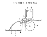
図1は、インクジェット記録ヘッド2を設けたプリンタ装置(インクジェット記録装置)の側面図である。図中、1は記録媒体であり、プリンタ装置によって印字等の処理が施される。2はインクジェット記録ヘッドであり記録媒体1にインクを噴射する。3はインクタンクであり、インクジェット記録ヘッド2にインクを供給する。4はキャリッジであり、インクジェット記録ヘッド2とインクタンク3を搭載している。
【0005】
5は送りローラ、6はピンチローラであり、記録媒体1を挟持してインクジェット記録ヘッド2へと搬送する。7は排出ローラ、8はピンチローラであり、記録媒体1を挟持して排出方向へと搬送する。9はスタッカであり、排出された記録媒体1を収納する。10はプラテンであり、記録媒体1を押さえる。
インクジェット記録ヘッド2は、電圧を印加して圧電素子を伸縮させることにより生じた圧力によってインクを噴射し、これにより記録媒体1に印字等の処理を行なう構成とされている。
【0006】
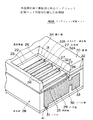
このインクジェット記録ヘッド2の斜視断面図を図2に示す。同図に示すように、インクジェット記録ヘッド2は、複数の圧電体11と、この圧電体11上に形成した個別電極12と、ノズル17が設けられたノズル板13と、振動板15と、各ノズル17に対応して形成されたインク室14(圧力室)を有する金属または樹脂からなる本体部16等にから構成されている。
【0007】
ノズル13および振動板15はインク室14に対し対向するよう配設されており、また本体部16のインク室14の周辺と振動板15とは強固に固定されている。また、圧電体11に電圧印加され駆動することにより、振動板15は図中点線にて示す様に変形する構成となっている。また、個々の圧電体11への電圧印加は、印字装置本体(図示せず)からの電気信号に基づき行なわれる構成となっている。
【0008】
上記した従来構成のインクジェット記録ヘッド2では、圧電体11を振動板15上に形成するのに、板状の圧電体11を振動板15のインク室形成位置と対応する位置に貼り付けるか、又は、予め振動板15の上面全面に圧電体部材を形成しておき、その後にインク室形成位置と対応する位置を除き圧電体部材を除去することにより、圧電体11を形成することが行なわれていた。
【0009】
尚、図2に示す例では、振動板15を変位させる手段として圧電体11を用いたが、圧電体11に代えて発熱体を用いたインクジェット記録ヘッドも提供されている。この発熱体を用いたインクジェット記録ヘッドは、発熱体を加熱させることにより発生する熱膨張により振動板15を変位させ、これによりインクを吐出させる構成とされている。以下、上記した圧電体11及び発熱体を含め、振動板15を変位させるエネルギーを発生させるものをインク吐出エネルギー発生部というものとする。
【0010】
【発明が解決しようとする課題】
ところで、近年ではパーソナルコンピュータの低消費電力化が要望されており、これに伴い周辺機器であるプリンタ装置においても低消費電力化(半導体駆動電圧化:〜20V)が要求されるようになってきている。また、一方においてプリンタ装置には高い解像度が要求されており、これに伴いインクジェット記録ヘッド2の微細化が急速に進められている。
【0011】
具体的には、これらの要求を実現化するためには次の事項が必要となる。即ち、インク吐出エネルギー発生部に圧電体を用いる場合には、
a)圧電体の薄膜化(内部印加電界は同じ)
b)振動板の薄膜化(圧電体の微小変位伝達)
c)圧電体と振動板の密着安定性(圧電体の変形ロス低減)
d)振動板の平坦性向上(振動板の曲がり易さ)
e)圧電体および振動板の微細加工
が必要となる。
【0012】
また、インク吐出エネルギー発生部に発熱体を用いる場合には、
f)発熱体までの配線の微細化
g)放熱時間の短縮化
h)発熱素子保護膜の薄膜化
等が必要となる。
【0013】
しかるに、図2を用いて説明した従来のインクジェット記録ヘッド2では、以下に示す問題がある。即ち、圧電体を振動板に張り付ける構成では、
▲1▼圧電体を振動板に張り付ける際、薄い圧電体は壊れ易い。
▲2▼圧電体を振動板に張り付ける構成では、接着剤層の厚さが不均一となり振動板を平坦とすることが困難で、よって駆動させた際に適正に変形しない場合が生じる。
【0014】
▲3▼圧電体に電圧印加した際、接着剤が圧電体の変位を吸収してしまう。
▲4▼圧電体を振動板に張り付ける構成では、微細化に対応できない。
という問題点がある。
また、振動板全面に配設された圧電体部材を機械加工で分割する構成では、上記した▲1▼〜▲4▼の問題点が同様に発生する。更に、機械加工では加工時間が長く要し、製造効率が悪いという問題点もある。
【0015】
更に、インク吐出エネルギー発生部に発熱体を用いた場合には、発熱体を形成した基板が必ずしも放熱特性に優れているとは限らないという問題点がある。
本発明は上記の点に鑑みてなされたものであり、高信頼性を維持しつつ消費電力の低減を図りうるインクジェット記録ヘッド及びその製造方法及びプリンタ装置を提供することを目的とする。
【0016】
【課題を解決するための手段】
上記課題を解決するために本発明では、次に述べる各手段を講じたことを特徴とするものである。請求項1の発明は、インクを吐出するノズルに対応して設けられており、内部にインクが充填される複数の圧力室が形成されてなる本体部と、振動可能な材料により形成されており、前記圧力室の一の壁面を構成する振動板と、前記圧力室と対応する前記振動板上に配設されており、前記振動板を変形することにより前記圧力室内のインクを前記ノズルから吐出させるインク吐出エネルギー発生部とを有するインクジェット記録ヘッドにおいて、薄膜形成技術を用いて、基板上に、前記インク吐出エネルギー発生部を構成する個別電極層及びエネルギー発生層を形成し、さらにその上に振動板を形成するとともに、前記基板の少なくとも前記インク吐出エネルギー発生部の変形領域に対応する領域を除去することにより形成された、前記基板から前記インク吐出エネルギー発生部を露出させるための開口部を有することを特徴とするものである。
【0017】
また、請求項2記載の発明に係るインクジェット記録ヘッドの製造方法は、基板上に薄膜形成技術を用いて個別電極層、エネルギー発生層、振動板を順次形成することによりインク吐出エネルギー発生部を形成するエネルギー発生部形成工程と、前記基板の少なくとも前記インク吐出エネルギー発生部の変形領域に対応する領域を除去して開口部を形成することにより、前記基板から前記インク吐出エネルギー発生部を露出させる除去工程と、予めインクを吐出するための圧力室が形成されてなる本体部材を前記振動板に接合する接合工程と、前記圧力室と対応する位置にインクを吐出するノズル孔が形成されると共に、前記本体部材にノズル板を配設するノズル板配設工程と、を有することを特徴とするものである。
【0018】
また、請求項3記載の発明は、前記請求項2記載のインクジェット記録ヘッドの製造方法において、前記接合工程は、前記エネルギー発生部形成工程と前記除去工程との間に実施され、前記振動板上に、予めインクを吐出するための第1の圧力室半体が形成されてなる第1の本体部材半体を接合する第1の接合工程と、前記除去工程の終了後、予めインクを吐出するための第2の圧力室半体が形成されてなる第2の本体部材半体を前記第1の本体部材半体に接合する第2の接合工程とよりなることを特徴とするものである。
【0019】
また、請求項4記載の発明は、前記請求項2または請求項3記載のインクジェット記録ヘッドの製造方法において、前記エネルギー発生部形成工程は、前記個別電極層を形成した後で、かつ前記エネルギー発生層を形成する前に、前記インク吐出エネルギー発生部の形成位置で前記個別電極層を分割し、個別電極を形成する分割工程を有することを特徴とするものである。
【0020】
また、請求項5記載の発明は、前記請求項2または3記載のインクジェット記録ヘッドの製造方法において、前記エネルギー発生部形成工程は、前記除去工程を終了した後に、前記開口部に露出した前記個別電極層と前記エネルギー発生層とを前記インク吐出エネルギー発生部の形成位置において共に分割し、個別電極を形成する分割工程を有することを特徴とするものである。
【0021】
また、請求項6記載の発明は、前記請求項2または3記載のインクジェット記録ヘッドの製造方法において、前記エネルギー発生部形成工程は、前記除去工程を終了した後に、前記開口部に露出した前記個別電極層のみを前記インク吐出エネルギー発生部の形成位置において分割し、個別電極を形成する分割工程を有することを特徴とするものである。
【0022】
また、請求項7記載の発明は、前記請求項6記載のインクジェット記録ヘッドの製造方法において、前記エネルギー発生部形成工程で、複数の前記圧力室にまたがるよう前記インク吐出エネルギー発生部を形成することを特徴とするものである。また、請求項8記載の発明に係るインクジェット記録ヘッドの製造方法は、基板上に薄膜形成技術を用いてインク吐出エネルギー発生部となるエネルギー発生層及び振動板を順次形成するエネルギー発生部形成工程と、前記基板の少なくとも前記インク吐出エネルギー発生部の変形領域に対応する領域を除去して開口部を形成することにより、前記基板から前記インク吐出エネルギー発生部を露出させる除去工程と、該除去工程の終了後、前記開口部を介して前記インク吐出エネルギー発生部と対応する位置に個別電極を形成する個別電極形成工程と、予めインクを吐出するための圧力室が形成されてなる本体部材を前記振動板に接合する接合工程とを有することを特徴とするものである。
【0023】
また、請求項9記載の発明は、前記請求項4乃至7のいずれかに記載のインクジェット記録ヘッドの製造方法において、前記分割工程で前記分割処理を行う分割位置を、隣り合う前記圧力室の間位置に設定したことを特徴とするものである。
【0024】
また、請求項10記載の発明に係るインクジェット記録ヘッドの製造方法は、基板上に薄膜形成技術を用いて個別電極層を形成する個別電極形成工程と、少なくとも前記個別電極層上に個別エネルギー発生層を形成する個別エネルギー発生層形成工程と、前記個別エネルギー発生層形成工程で形成された前記個別エネルギー発生層間の空隙部分に充填材を配設する充填工程と、前記充填工程終了後に、前記個別エネルギー発生層及び前記充填材の上部に振動板を形成する振動層形成工程とを実施することによりインク吐出エネルギー発生部を形成するエネルギー発生部形成工程と、前記基板の少なくとも前記インク吐出エネルギー発生部の変形領域に対応する領域を除去して開口部を形成することにより、前記基板から前記インク吐出エネルギー発生部を露出させる除去工程と、予めインクを吐出するための圧力室が形成されてなる本体部材を前記振動板に接合する接合工程とを有することを特徴とするものである。
【0025】
また、請求項11記載の発明は、前記請求項10記載のインクジェット記録ヘッドの製造方法において、前記充填材として、前記基板と同一材料を用いたことを特徴とするものである。また、請求項12記載の発明は、前記請求項10記載のインクジェット記録ヘッドの製造方法において、前記充填材として、ヤング率が前記エネルギー発生層の材料よりも小さく、90GPa以下であるものを用いたことを特徴とするものである。
【0026】
また、請求項13記載の発明は、前記請求項10乃至12のいずれかに記載のインクジェット記録ヘッドの製造方法において、前記充填材として、弾性及び耐インク性のある材料を用いたことを特徴とするものである。
【0027】
また、請求項14記載の発明は、前記請求項2記載のインクジェット記録ヘッドの製造方法において、前記接合工程を実施した後に、前記除去工程を実施することを特徴とするものである。また、請求項15記載の発明は、前記請求項2乃至14のいずれかに記載のインクジェット記録ヘッドの製造方法において、前記ノズル板配設工程を前記接合工程の前に実施することを特徴とするものである。
【0028】
また、請求項16記載の発明は、前記請求項2乃至14のいずれかに記載のインクジェット記録ヘッドの製造方法において、前記ノズル板配設工程を前記接合工程の後に実施することを特徴とするものである。
【0029】
また、請求項17記載の発明は、前記請求項2乃至16のいずれかに記載のインクジェット記録ヘッドの製造方法において、更に、前記除去工程を実施した後に、前記基板に形成した開口部に熱伝達性の高い材料を配設する放熱部形成工程を実施することを特徴とするものである。
【0030】
また、請求項18記載の発明は、圧力室と圧電体からなり、電気信号により前記圧電体を変形させて、前記圧力室内部のインクを吐出させるインクジェット記録ヘッドにおいて、前記圧電体を基板上に薄膜形成技術を用いて成長させる成長工程と、前記圧電体の変形する部分の周囲の基板を残し、前記圧電体の変形する部分の基板を除去し、前記基板から前記インク吐出エネルギー発生部を露出させるための開口部を形成する除去工程とにより形成された圧電体を用いたことを特徴とするものである。
【0031】
また、請求項19記載の発明は、圧力室と圧電体からなり、電気信号により前記圧電体を変形させて、前記圧力室内部のインクを吐出させるインクジェット記録ヘッドを用いたプリンタ装置において、前記圧電体を基板上に薄膜形成技術を用いて成長させる成長工程と、前記圧電体の変形する部分の周囲の基板を残し、前記圧電体の変形する部分の基板を除去し、前記基板から前記インク吐出エネルギー発生部を露出させるための開口部を形成する除去工程とにより形成された圧電体を用いたインクジェット記録ヘッドを有することを特徴とするものである。
【0032】
上記した各手段は、次のように作用する。請求項1記載の発明によれば、振動板及びインク吐出エネルギー発生部の内、少なくともインク吐出エネルギー発生部を薄膜形成技術を用いて形成したことにより、薄くかつ微細化されたインク吐出エネルギー発生部を高精度にかつ高信頼性をもって形成することができる。よって、低消費電力化を図ることができると共に、高解像度の印刷を可能とすることができる。
【0033】
また、請求項2及び請求項18記載の発明によれば、エネルギー発生部形成工程において、基板上に薄膜形成技術を用いて個別電極層、エネルギー発生層、振動板を順次形成しインク吐出エネルギー発生部を形成するため、薄いインク吐出エネルギー発生部を高精度にかつ高信頼性をもって形成することができる。
【0034】
また、各層間には接着材等の他の接合部材は介在しないため、高い平坦性を有したインク吐出エネルギー発生部を形成することが可能となり、従来のように接着材が圧電体の変位を吸収するようなこともない。よって、低消費電力化及び印刷の高解像度化を図りうるインクジェット記録ヘッドを実現することができる。また、除去工程において、基板の所定領域を除去して開口部を形成し基板からインク吐出エネルギー発生部を露出させるため、この露出部分以外は基板に保護された状態を維持される。よって、インク吐出エネルギー発生部が薄型化されても、この保護を確実に行なうことができる。
【0035】
続いて接合工程及びノズル板配設工程実施することにより、上記のインク吐出エネルギー発生部は、圧力室が形成された本体部に接合される。よって、圧力室に平坦な振動板を配設することができ、圧電体と振動板との密着性が良好で、かつ、ばらつきの無い効率良い駆動を行いうるインクジェット記録ヘッドを製造することができる。
【0036】
また、請求項3記載の発明によれば、エネルギー発生部形成工程と除去工程との間、即ち除去工程を実施する前に第1の接合工程を実施し、振動板上に第1の圧力室半体が形成されてなる第1の本体部材半体を接合することにより、基板は第1の本体部材半体により補強された構成となる。
【0037】
よって、除去工程において開口部を形成する際、開口部形成位置の背面側には第1の本体部材半体が存在するため、インク吐出エネルギー発生部が開口形成時に損傷することを防止することができる。また、開口部が形成されることにより、この開口部から露出したインク吐出エネルギー発生部の機械的強度は低下するが、開口部形成位置の背面側に補強材として機能する第1の本体部材半体が存在するため、開口部の形成後においてもインク吐出エネルギー発生部が損傷することを防止することができる。
【0038】
また、除去工程の終了後に第2の接合工程を実施し、第2の圧力室半体が形成された第2の本体部材半体を第1の本体部材半体に接合することにより、第1及び第2の圧力室半体は協働して圧力室を形成し、よって本体部が形成される。また、請求項4記載の発明によれば、個別電極層を形成した後、かつエネルギー発生層を形成する前に分割工程を実施し、インク吐出エネルギー発生部の形成位置で個別電極層を分割して個別電極を形成することにより、開口部を形成する前において個別電極が形成されているため、開口部を介して個別電極層を分割する方法に比べ、容易に個別電極を形成することができる。
【0039】
また、請求項5記載の発明によれば、除去工程を終了した後に分割工程を実施し、開口部に露出した個別電極層とエネルギー発生層とをインク吐出エネルギー発生部の形成位置において共に分割して個別電極を形成することにより、隣接するインク吐出エネルギー発生部は完全に独立した構成となる。よって、電圧印加した際にインク吐出エネルギー発生部の変形性(駆動性)は向上し、これにより確実で応答性のよいインク吐出を行うことができる。
【0040】
また、請求項6記載の発明によれば、除去工程を終了した後に分割工程を実施し、開口部に露出した個別電極層のみをインク吐出エネルギー発生部の形成位置において分割して個別電極を形成することにより、内部歪みの少ないインク吐出エネルギー発生部を形成することができる。
【0041】
即ち、分割工程をエネルギー発生層を配設する前に分割し個別電極を形成する方法では、エネルギー発生層を形成する際、基板上に直接エネルギー発生層が積層される部分と、個別電極上にエネルギー発生層が積層される部分とが発生してしまう。これにより、エネルギー発生層には、格子定数の違い等からくる内部歪みが発生し易くなる。この状態のままで、基板に開口部を形成すると、除去後の薄膜部分で内部歪みからくる損傷(ヒビや変形)が発生する可能性がある。
【0042】
しかるに、基板上の全面に個別電極層を形成すると共にその上にエネルギー発生層を形成し、除去工程を終了した後に分割工程を実施して開口部を介して個別電極層を分割することにより、内部歪みの少ないインク吐出エネルギー発生部を形成することができ、製造されるインクジェット記録ヘッドの信頼性を向上させることができる。
【0043】
また、請求項7記載の発明によれば、エネルギー発生部形成工程で、複数の圧力室にまたがるようインク吐出エネルギー発生部を形成することにより、インク吐出エネルギー発生部の強度を向上させることができる。即ち、圧力室の形成領域内にインク吐出エネルギー発生部を形成すると、圧力室は空間部であるためインク吐出エネルギー発生部は薄い振動板にのみ保持された構成となり強度が低下する。しかるに、複数の圧力室にまたがるようインク吐出エネルギー発生部を形成することにより、インク吐出エネルギー発生部は圧力室外周部の基板により保持されることとなり、インク吐出エネルギー発生部の強度を向上させることができる。
【0044】
また、請求項8記載の発明によれば、エネルギー発生部形成工程において、基板上に薄膜形成技術を用いてインク吐出エネルギー発生部となるエネルギー発生層を基板の格子定数に従い単結晶状態で成長させることができる(格子定数は同じでなく、内部歪みを有している)。
【0045】
いま、基板とエネルギー発生層との間に結晶格子を持たない金属電極層(個別電極層)が介在すると、エネルギー発生層の形成時にその格子が変形し、良好な吐出エネルギーを得られない場合がある。
しかるに、除去工程において基板に開口部を形成した後、開口部から露出したエネルギー発生層の表面に個別電極形成工程を実施し、個別電極を形成することにより、必要とする格子定数を有したインク吐出エネルギー発生部を形成することができ、良好な吐出エネルギーを得ることができる。よって、信頼性の高い印字処理を行なうことが可能となる。
【0046】
また、請求項9記載の発明によれば、分割工程で個別電極層を分割処理する分割位置を、隣り合う圧力室の間位置に設定したことにより、振動板の保護を確実に図ることができる。即ち、圧力室は空間部であるため、インク吐出エネルギー発生部(個別電極層を含む)は薄い振動板にのみ保持された構成となっている。よって、この圧力室の形成領域内において個別電極層の分割処理を行うと、振動板に亀裂等の損傷が発生する可能性がある。
【0047】
しかるに、個別電極層の分割位置を隣り合う圧力室の間位置に設定することにより、この分割位置は圧力室ではなく基板上の位置となるため、インク吐出エネルギー発生部は圧力室を跨いで形成される構成となり、振動板の保護を確実に行うことができる。また、請求項10記載の発明によれば、インク吐出エネルギー発生部間の空隙部分に充填材を配設することにより、平坦でかつ曲げに対して拘束しない構成が得られ、円滑なインク吐出を行うことが可能となる。
【0048】
即ち、充填材が存在しない凹凸を有したインク吐出エネルギー発生部上に振動板を形成すると、凹凸の段差部分において振動板の曲がりが発生し、この部分がインク吐出エネルギー発生部の変形を拘束しインク吐出に支障をきたすおそれがある。
しかるに、充填工程においてインク吐出エネルギー発生部間の空隙部分に充填材を配設することによりその上面は平坦化し、この平坦面上に振動板を形成することで、平坦でかつ曲げに対して拘束しない構成が得られる。このように曲げに対する拘束が無い構成とすることにより、円滑なインク吐出を行なうことが可能となる。
【0049】
また、請求項11記載の発明によれば、充填材として基板と同一材料を用いたことにより、後に実施される除去工程において開口部を形成する際、インク吐出エネルギー発生部間の充填材も同時に除去される。
このため各インク吐出エネルギー発生部は独立した構成となり、インク吐出エネルギー発生部の駆動性を向上させることができる。
【0050】
また、請求項12記載の発明によれば、充填材として低ヤング率の材料を用いたことにより、インク吐出エネルギー発生部間の空隙部分に充填材を配設しても、この充填材によりインク吐出エネルギー発生部の変形(変位)が妨げられるようなことはなく、確実なインク吐出を行うことができる。
【0051】
また、請求項13記載の発明によれば、充填材として弾性及び耐インク性のある材料を用いたことにより、充填材により圧力室からのインク漏れを防止することができる。即ち、稀ではあるが除去工程を実施することにより、開口部から露出した振動板にピンホール等が形成されてしまう場合がある。この場合、圧力室内のインクがピンホールから外に染み出し、インク吐出エネルギー発生部(圧電体)の電気部分でショート等の不良が発生するおそれがある。しかるに、振動板にピンホールがあっても機能的には問題なく、よってインクの染み出しさえ予防できれば良い。
【0052】
よって、開口部内のインク吐出エネルギー発生部間に弾性及び耐インク性を有する充填材を配設することにより、インク吐出エネルギー発生部の駆動(変形、変位)を損なわず、かつインクの染み出しを防止することができる。また、請求項14記載の発明によれば、接合工程を実施した後に除去工程を実施することにより、除去工程において開口部を形成する際、基板の背面側には本体部が接合された状態となっている。このため、開口部を形成する際に基板に形成されているインク吐出エネルギー発生部が損傷することを防止でき、歩留り及び信頼性の向上を図ることができる。
【0053】
また、請求項15及び請求項16記載の発明のように、ノズル板配設工程は接合工程の前に実施しても、また後に実施してもよい。また、請求項17に記載の発明によれば、除去工程を実施した後に放熱部形成工程を実施し、基板に形成した開口部に熱伝達性の高い材料を配設することにより、インク吐出エネルギー発生部で発生する熱を効率よく放熱することが可能となり、高速印字が可能となる。
【0054】
【発明の実施の形態】
次に、本発明の実施の形態について図面と共に説明する。
図3は本発明の第1実施例であるインクジェット記録ヘッド40Aを示す図であり、また図4及び図5は本発明の第1実施例であるインクジェット記録ヘッドの製造方法を説明するための図であり、本実施例では図1に示すインクジェット記録ヘッド40Aの製造方法を示している。尚、以下説明する各実施例においては、インク吐出を行なうエネルギー発生手段として圧電体を用いた例について説明するが、圧電体に代えて発熱体を用いることも可能である。
【0055】
まず、図1を用いてインクジェット記録ヘッド40Aの構成について説明する。インクジェット記録ヘッド40Aは、大略すると基板20,振動板23,本体部28,ノズル板30,及びインク吐出エネルギー発生部32A(以下、エネルギー発生部という)等により構成されている。
本体部28は後述するようにドライフィルムを積層した構造を有しており、その内部に複数の圧力室29(インク室)と、インクの供給路となるインク通路33とが形成されている。また、この圧力室29の図中上部は開放部とされると共に、下面にはインク吐出孔41が形成されている。
【0056】
また、本体部28の図中下面にはノズル板30が配設されると共に、上面には振動板23が配設されている。ノズル板30は例えばステンレスによりなり、インク吐出孔41と対向する位置にノズル31が形成されている。
また、振動板23は例えばクロム(Cr)により形成された可撓性を有する板状材であり、その上部には基板20及びエネルギー発生部32Aが配設されている。基板20は例えば酸化マグネシウム(MgO)により形成されており、その中央位置には開口部24が形成されている。エネルギー発生部32Aは、この開口部24により露出された振動板23上に形成されている。
【0057】
エネルギー発生部32Aは、前記した振動板23(共通電極としても機能する)上に形成され、個別電極26、及び圧電体27により構成されている。このエネルギー発生部32Aは、本体部28に複数形成されている圧力室29の形成位置と対応する位置に形成されている。個別電極26は例えば白金(Pt)よりなり、圧電体27の上面に形成されている。また、圧電体27は圧電気を生じる結晶体であり、本実施例では各圧力室29の形成位置にそれぞれ独立して形成された構成となっている(即ち、隣接するエネルギー発生部32Aは連続していない)。
【0058】
上記構成とされたインクジェット記録ヘッド40Aにおいて、共通電極としても機能する振動板23と個別電極26との間に電圧印加をすると、圧電体27は圧電気現象により歪みを発生する。このように圧電体27に歪みが発生すると、これに伴い振動板23も変形する。
この時に圧電体27に発生する歪みは、振動板23が図中破線で示すような変形となるよう、即ち圧力室29に向け凸となる形状に変形するよう構成されている。よって、圧電体27の歪みに伴う振動板23の変形により、圧力室29内のインクは加圧され、インク吐出孔41及びノズル31を介して外部に吐出され、これにより記録媒体に印刷が行なわれる構成となっている。
【0059】
上記構成において、本実施例に係るインクジェット記録ヘッド40Aは、振動板23及びエネルギー発生部32(個別電極26,圧電体27)を薄膜形成技術を用いて形成したことを特徴としている(詳細な製造方法については、後述する)。
このように、振動板23及びエネルギー発生部32を薄膜形成技術を用いて形成するにより、薄くかつ微細化されたエネルギー発生部32を高精度にかつ高信頼性をもって形成することができる。よって、インクジェット記録ヘッド40Aの低消費電力化を図ることができると共に、高解像度の印刷を可能とすることができる。
【0060】
また、本実施例では各エネルギー発生部32毎に圧電体27が分割された構成とされている。即ち、各エネルギー発生部32は、隣接するエネルギー発生部32に拘束されることなく変位することができる。よって、インク吐出に必要とされる印加電圧を低くするこができ、これによってもインクジェット記録ヘッド40Aの低消費電力化を図ることができる。
【0061】
続いて、上記構成とされたインクジェット記録ヘッド40Aの製造方法について図4及び図5を用いて説明する。
インクジェット記録ヘッド40Aを製造するには、先ず図4(A)に示されるように、基板20を用意する。本実施例では、基板20として厚さが0.3mm の酸化マグネシウム(MgO)単結晶体を用いている。
【0062】
この基板20上には、薄膜形成技術であるスパッタリング法を用い、個別電極層21(以下、単に電極層という),エネルギー発生層22(本実施例では圧電体を用いているため、以下圧電体層という),振動板23を順次形成する(エネルギー発生部形成工程の一部を成す)。具体的には、先ず図4(B)に示すように基板20上に電極層21を形成し、続いて図4(C)に示すように電極層21上に圧電体層22を形成し、更に圧電体層22上に振動体23を形成する。尚、本実施例では、電極層21の材質として白金(Pt)を、また振動板23の材質としてNi−Cr,Cr等を用いている。
【0063】
上記のように、薄膜形成技術を用いた各層21〜23の形成処理が終了すると、続いて図5(E)に示すように、各層21〜23が下側になるよう基板20を上下反転すると共に、この基板20の略中央部分をエッチングにより除去することにより開口部24を形成する(除去工程)。
この開口部24の形成位置は、少なくともエネルギー発生部32A(図3参照)により振動板23が変形する変形領域と対応するよう選定されている。このように基板20を除去して開口部24を形成することにより、図5(F)に示すように、電極層21は開口部24を介し基板20から露出した構成となる。
【0064】
上記のように除去工程を実施することにより開口部24が形成されると、続いて開口部24に露出した電極層21と圧電体層22を所定位置(圧力室29の形成位置と対応する位置)において共に分割し、エネルギー発生部32Aを形成する(分割工程。この分割工程はエネルギー発生部形成工程の一部を成す)。このエネルギー発生部32Aの幅寸法は、後に実施される接合工程において本体部28を基板20に接合した際、エネルギー発生部32Aが複数の圧力室29をまたがるよう設定されている。
【0065】
上記の分離工程を行なうことにより電極層21は分割されて個別電極となり、よって各圧力室29毎にインクの吐出制御を行なうことが可能となる。また、圧電体層22は分割処理されることにより、個々独立した圧電体27を形成する。一方、圧力室29を有した本体部28及びノズル板30は、上記した工程と別工程を実施することにより形成される。圧力室29を有した本体部28は、ノズル板30(アライメントマーク付)にドライフィルム(東京応化製溶剤型ドライフィルムPRシリーズ)をラミネート・露光を必要回数だけ現像することにより形成される(ノズル板配設工程)。
【0066】
具体的な本体部28の形成方法は、次の通りである。即ち、ノズル板30(厚さ20μm )上にノズル31(20μm 径、ストレート穴)まで圧力室29からのインクを誘導し、且つインクの流れを一方向に揃えるためのインク通路33(60μm 径;深さ60μm )のパターンをノズル板30のアライメントマークを用いて露光し、続いて圧力室29(幅100μm ,長さ1700μm ,厚さ60μm )をインク通路33と同様にノズル板30のアライメントマークを用いて露光し、その後10分の自然放置(室温)と加熱硬化(60℃,10分)を行い、溶剤現像によりドライフィルムの不要部分を除去する。
【0067】
上記のように形成されたノズル板30が設けられた本体部28は、図5(G)に示すように、振動板23に接合される(接合固定)。この際、圧力室29とエネルギー発生部32Aとが精度よく対向するよう接合処理される。
上記のように本実施例によれば、基板20上にスパッタリング法等の薄膜形成技術を用いて電極層21,圧電体層22,振動板23を順次形成しエネルギー発生部32Aを形成するため、従来に比べて薄いエネルギー発生部32Aを高精度にかつ高信頼性をもって形成することができる。
【0068】
また、各層21〜23の間には接着材等の他の接合部材は介在しないため、高い平坦性を有したエネルギー発生部32Aを形成することが可能となり、従来のように接着材が圧電体の変位を吸収するようなこともない。よって、低消費電力化及び印刷の高解像度化を図りうるインクジェット記録ヘッド40Aを実現することができる。また、振動板23が平坦化することにより、圧電体27と振動板23との密着性が良好となり、ばらつきの無い効率良い駆動を行いうるインクジェット記録ヘッド40Aを実現することができる。
【0069】
また、上記した除去工程においては、基板20の所定領域を除去して開口部24を形成することにより基板20からエネルギー発生部32Aを露出させるため、従来のように圧電体11等が単に露出した構成(図2参照)に比べ、エネルギー発生部32Aの保護を行なうことができる。よって、エネルギー発生部32Aが薄型化されても損傷するようなことはなく、インクジェット記録ヘッド40Aの信頼性を向上させることができる。
【0070】
また、本実施例では除去工程を終了した後に分割工程を実施し、開口部24に露出した電極層21と圧電体層22を共に分割して個別電極26,圧電体27を形成することにより、隣接するエネルギー発生部32Aは完全に独立した構成となる。よって、電圧印加した際にエネルギー発生部32Aの変形性(駆動性)は向上し、応答性のよいインク吐出を行なうことが可能となる。
【0071】
更に、上記したように本実施例では、エネルギー発生部32Aが複数の圧力室29にまたがるよう形成されているため、エネルギー発生部32Aは圧力室29の外周部の基板20により保持されることとなる。よって、エネルギー発生部32Aの強度を向上させることができ、インクジェット記録ヘッド40Aの信頼性を向上させることができる。
【0072】
続いて、図6乃至図8を用い、本発明の第2実施例であるインクジェット記録ヘッド40B及びその製造方法について説明する。
図6は本発明の第2実施例であるインクジェット記録ヘッド40Bを示す図であり、また図7及び図8は本発明の第2実施例であるインクジェット記録ヘッド40Bの製造方法を説明するための図である。
【0073】
尚、以下説明する各実施例において、図3を用いて説明した第1実施例に係るインクジェット記録ヘッド40Aの構成と同一構成については、同一符号を付してその説明を省略する。また同様に、以下説明する各実施例において、図4及び図5を用いて説明した第1実施例に係る製造工程と同一工程についても、その説明を省略するものとする。
【0074】
図6に示されるように、本実施例に係るインクジェット記録ヘッド40Bは、圧電体27は分割されておらず、個別電極26のみが圧力室29に対応して分割形成された構成となっている。従って、隣接する個別電極26の間には圧電体27が存在した構成となっている。また、後に詳述するように、個別電極26は開口部24を形成した後に形成される構成となっている。
【0075】
続いて、上記構成とされたインクジェット記録ヘッド40Bの製造方法について説明する。
前記した第1実施例に係る製造方法では、基板20の上面に先ず電極層21を形成したが(図4(B)参照)、本実施例では基板20の上面に先ずスパッタリング法を用いて圧電体層22を形成することを特徴としている(図7(B))。即ち、本実施例では電極層21を形成することなく、基板20の上面に直接圧電体層22を形成する構成としている。この際、基板20の上面が〔100〕面となるよう設定されいてる。
【0076】
また本実施例では、個別電極26を形成する個別電極形成工程は、図8(E),(F)に示されるように、除去工程が終了した後(即ち、開口部24が形成された後)に実施することを特徴としている。
上記のように、電極層21を形成することなく基板20の上面に直接圧電体層22を形成することにより、開口部24を形成した際、図8(D)に示されるように、開口部24には圧電体27(圧電体層22)が露出した状態となる。個別電極26は、この開口部24を介して圧電体27(圧電体層22)の上面に薄膜形成技術を用いて形成される。この際、個別電極26の形成位置は、エネルギー発生部32Bの所定形成位置と対応する位置に設定されている。
【0077】
本実施例のように、基板20上に薄膜形成技術を用いて圧電体27(圧電体層22)及び振動板23を順次形成することにより、圧電体27(圧電体層22)を基板20の格子定数に従い単結晶状態で成長させることができる(格子定数は同じでなく、内部歪みを有している)。
第1実施例のように、基板20と圧電体27(圧電体層22)との間に結晶格子を持たない金属電極層(電極層21)が介在すると、圧電体27(圧電体層22)の形成時にその格子が変形し、良好な吐出エネルギーを得られない場合がある。
【0078】
しかるに、除去工程において基板20に開口部24を形成した後、開口部24から露出した圧電体27(圧電体層22)の表面に個別電極26を形成することにより、必要とする格子定数を有した圧電体27(圧電体層22)を形成することがでる。これにより、良好な吐出エネルギーを得ることができ、よって信頼性の高い印字処理を行なうことが可能となる。
【0079】
続いて、図9乃至図11を用い、本発明の第3実施例であるインクジェット記録ヘッド40C及びその製造方法について説明する。
図9は本発明の第3実施例であるインクジェット記録ヘッド40Cを示す図であり、また図10及び図11は本発明の第3実施例であるインクジェット記録ヘッド40Cの製造方法を説明するための図である。
【0080】
図9に示されるように、本実施例に係るインクジェット記録ヘッド40Cは、第2実施例であるインクジェット記録ヘッド40Bと同様に、圧電体27(圧電体層22)は分割されておらず、個別電極26のみが圧力室29に対応して分割形成された構成となっている。
続いて、上記構成とされたインクジェット記録ヘッド40Cの製造方法について説明する。図10(A)〜図11(D)までの製造工程は、第1実施例と同様である。よって、除去工程を実施することにより形成された開口部24には、電極層21が露出した状態となっている。
【0081】
本実施例に係る製造方法では、除去工程を終了した後に分割工程を実施し、開口部24に露出した電極層21のみをエネルギー発生部32Cの形成位置(図9及び図11(E)参照)において分割し、個別電極26を形成することを特徴とするものである。また、個別電極26を形成する際、電極層21の分割位置を、隣り合う圧力室29の間位置に設定したことを特徴としている。
【0082】
本実施例のように、除去工程を終了した後に分割工程を実施し、開口部24に露出した電極層21のみを分割し個別電極26を形成することにより、内部歪みの少ないエネルギー発生部32Cを形成することができる。
即ち、分割工程を圧電体層22を配設する前に分割し個別電極26を形成する方法では、圧電体層22を形成する際、基板20上に直接圧電体層22が積層される部分と、個別電極26上に圧電体層22が積層される部分とが発生してしまう。
【0083】
この構成では、圧電体層22に格子定数の違い等からくる内部歪みが発生し易くなる。そして、内部歪みが発生したままの状態で基板20に開口部24を形成すると、除去後の薄膜部分で内部歪みからくる損傷(ヒビや変形)が発生するおそれがある。
しかるに、本実施例のように、基板20の上面全面に電極層21を形成すると共にその上に圧電体層22を形成し、除去工程が終了した後に電極層21を分割することにより、内部歪みの少ない圧電体層22を形成することができ、製造されるインクジェット記録ヘッド40Cの信頼性を向上させることができる。
【0084】
また、分割工程で電極層21を分割処理する分割位置を、隣り合う圧力室29の間位置に設定したことにより、分割処理を確実に行なうことができる。即ち、圧力室29は空間部であるため、電極層21及び圧電体層22は薄い振動板23にのみ保持された構成となっている。よって、空間部である圧力室29の形成領域上において電極層21の分割処理を行なうと、振動板23に亀裂等の損傷が発生する可能性がある。
【0085】
しかるに、本実施例のように、電極層21の分割位置を隣り合う圧力室29の間位置に設定することにより、この分割位置は圧力室29ではなく本体部28上の位置となる。即ち、エネルギー発生部32Cは圧力室29をまたがるように形成された構成となり、よって振動板23に損傷を与えることを防止することができる。
【0086】
続いて、図12乃至図14を用い、本発明の第4実施例であるインクジェット記録ヘッド40D及びその製造方法について説明する。
図12は本発明の第4実施例であるインクジェット記録ヘッド40Dを示す図であり、また図13及び図14は本発明の第4実施例であるインクジェット記録ヘッド40Dの製造方法を説明するための図である。
【0087】
図12に示すように、本実施例に係るインクジェット記録ヘッド40Dは、本体部28が第1の本体部半体28Aと第2の本体部半体28Bを接合した構成としたことを特徴とするものである。
この構成のインクジェット記録ヘッド40Dを製造するには、先ず図13(A)に示すように、上面が[100]面とされると共に厚さ約300μm のMgO製の基板20を用意する。そして、この基板20の上面には、スパッタリング法を用いてPtよりなる電極層21が約0.2 μm の厚さで形成される。
【0088】
続いて本実施例では、圧電体層22を形成する前に分割工程を実施し、図13(B)に示すように、エネルギー発生部32Cの形成位置(図12参照)で電極層21を分割して個別電極26(サイズ:80μm ×1900μm 、ピッチ:169μm )を形成する。この個別電極26を形成はフォトエッチングを用いて行い、また個別電極26の形成と共に後述する接合工程で用いるアライメントマーク(図示せず)も形成する。そして、基板20上に個別電極26を形成した上で、図13(C),(D)に示すように圧電体層22(厚さ3μm),振動板23(厚さ2μm)を順次薄膜形成技術を用いて形成する。
【0089】
続いて、図14(E)に示されるように、先ほど電極層21に形成したアライメントマークを利用し、振動板23の上部に第1の本体部半体28Aを形成する(第1の接合工程)。この第1の本体部半体28Aは、ドライフィルム(東京応化製溶剤型ドライフィルムPRシリーズ)をラミネート・露光を必要回数行い現像することにより形成される。この際、第1の圧力室半体29A及びインク通路33の半体も合わせて形成される。
【0090】
続いて、第1の本体部半体28Aが下に位置するよう基板20を反転させ、基板10側から電極層21のアライメントマークを用いて圧力室29に対応する部分のみが露出するようにマスキング処理を行う。この際、MgOよりなる基板10は無色透明であるので、マスキング処理を容易に行なうことができる。
このマスキング処理が終了すると、続いて酸性のエッチング液(例えば、50%りん酸溶液)にて基板10をエッチングし、図14(F)に示すように、開口部24を形成する(除去工程)。前記したように、本実施例では電極層21を基板に形成した直後に分割処理を行い個別電極26を形成しているため、開口部24を形成することにより個別電極26が露出する構成となる。よって、先に述べた開口部24を介して個別電極層26を分割する方法に比べ、個別電極26を容易に形成することができる。
【0091】
続いて、図14(H)に示されるように、第1の本体部半体28Aにノズル板30が配設された第2の本体部半体28Bが接合される(第2の接合工程)。この第2の本体部半体28Bは、上記した工程と別工程において形成される。即ち、第2の本体部半体28Bを形成するには、ノズル板30(アライメントマーク付)にドライフィルム(東京応化製溶剤型ドライフィルムPRシリーズ)をラミネート・露光を必要回数行い現像することにより形成される。この際、第2の圧力室半体29B及びインク通路33の半体も合わせて形成される。
【0092】
上記のように、第1の本体部半体28Aに第2の本体部半体28Bを接合する際、各本体部半体28A,28Bに設けられたアライメントマークを用いて位置決めし接合する。これにより、各本体部半体28A,28Bを位置決め精度よく接合することができる。尚、ドライフィルム製の第1及び第2の本体部半体28A,28Bの接合は、例えば15kgf/cm2 の圧力印加状態で150℃・14時間の加熱硬化条件下で行った。
【0093】
上記のように第1及び第2の本体部半体28A,28Bが接合することにより、第1及び第2の本体部半体28A,28Bは協働して本体部28を形成し、また第1及び第2の圧力室半体29A,29Bも接合して圧力室29を形成し、これにより図12に示すインクジェット記録ヘッド40Dが製造される。
上記したように本実施例では、除去工程を実施する前に第1の接合工程を実施し、振動板23上に第1の本体部材半体28Aを接合するため、除去工程時には基板10は第1の本体部材半体28Aにより補強された構成となる。よって、除去工程において開口部24を形成する際、開口部形成位置の背面側には第1の本体部材半体28Aが補強材として存在するため、振動板23,個別電極26,及び圧電体27等が開口形成時に損傷することを防止することができる。
【0094】
また、開口部24が形成されることにより、この開口部24から露出したエネルギー発生部32Cの機械的強度は低下するが、開口部形成位置の背面側に補強材として機能する第1の本体部材半体28Aが存在するため、開口部形成時ばかりでなく、開口部24の形成が終了した後においても、エネルギー発生部32Cの損傷を防止することができる。
【0095】
続いて、図15及び図16を用い、本発明の第5実施例であるインクジェット記録ヘッドの製造方法について説明する。尚、本実施例の説明において、前記した第4実施例に係るインクジェット記録ヘッドの製造方法と同一工程についてはその説明を省略するものとする。
本実施例においても、先ずMgOよりなる基板20([100]面,厚さ300μm )上にスパッタリング法にてPtよりなる電極層21(厚さ0.2 μm )を形成する。そして、形成された電極層21にフォトエッチングにより、アライメントマークと個別電極26を形成する(個別電極形成工程)。アライメントマークは、後に圧力室29の形成及び接合工程で位置決めに用いるものであり、また複数の個別電極部26(サイズ;80μm ×1900μm )は169μm ピッチで形成される(図15(A),(B))。
【0096】
続いて、個別電極部26が形成された電極層21上に、圧電体材料をスパッタリング法にて約3μm の厚さで積層し、その後エッチングすることにより個別圧電体34及び枠体35を形成する(個別エネルギー発生層形成工程)。個別圧電体34は、個別電極部26と同サイズとなるよう形成され、また枠体35は基板20の外周を囲繞するよう形成される。
【0097】
尚、この状態では、図15(C)に示すように、隣接する個別圧電体34の間には間隙部が形成されており、よって基板20の上面は複数の凹凸(段差)が形成された状態となっている。
続いて、MgOをターゲットとするスパッタリングを行い、隣接する個別圧電体34の間に充填材36を形成する(充填工程)。この際、個別圧電体34及び枠体35にはマスキングを行ない、個別圧電体34の間にのみ充填材36となるMgOを配設する。
【0098】
上記のように、本実施例では充填材36の材質として、基板20の材質と同材質が選定されている。また、充填材36の厚さは、前記した個別圧電体34及び枠体35と同一厚さとなるようスパッタリング制御が行なわれている。よって、充填材36が形成された状態において、個別圧電体34,枠体35,及び充填材36が協働して形成する面の表面は平坦化された面となる。
【0099】
上記のように充填工程が終了すると、続いて個別圧電体34,枠体35,及び充填材36を覆うようにCrよりなる振動体23が2μm の厚さでスパッタリングされる。これにより、基板20上にエネルギー発生部32D(図16(D)参照)が形成される。
本実施例のように、充填工程を実施し隣接する個別圧電体34の間に充填材36を形成することにより、円滑なインク吐出を行なうことが可能となる。即ち、充填材が存在しない凹凸を有した個別圧電体34上に振動板23を形成すると、凹凸の段差部分において振動板23の曲がりが発生し、この部分がエネルギー発生部32Dの変形を拘束しインク吐出に支障をきたすおそれがある。
【0100】
しかるに、充填工程において充填材36を配設することにより、個別圧電体34,枠体35,及び充填材36が協働して形成する面の表面は平坦化し、この平坦面上に振動板23を形成することで、平坦でかつ曲げに対して拘束しない構成が得られる。このように曲げに対する拘束が無い構成とすることにより、円滑なインク吐出を行なうことが可能となる。
【0101】
上記のように振動板3が形成されると、続いて先に述べた第4実施例と同様に第1の本体部半体28Aが振動板23の上部に配設され(図16(F))、その後に除去工程が実施されて基板20に対して開口部24が形成される。
この際、前記したように充填材36は基板20の材質と同材質が選定されているため、除去工程において開口部24を形成する際、開口部24と対応する位置における充填材36は基板20と共に除去される。即ち、開口部24から露出した各エネルギー発生部32Dは夫々独立した状態となる。
【0102】
このように、各エネルギー発生部32Dが独立した構成となることにより、各エネルギー発生部32Dの駆動性を向上させることができ、よって低消費電力化を図ることができる。
続いて、前記した第4実施例と同様にノズル板30が配設された第2の本体部半体28Bを第1の本体部半体28Aに接合するこにとより本体部28を形成し、これによりインクジェット記録ヘッドが形成される。
【0103】
ところで、上記した実施例では、充填材36として基板20の材質と同一材質とした構成としたが、他の材料を用いることも可能である。例えば、充填材36として低ヤング率の材料を用いることにより、隣接するエネルギー発生部32D間の空隙部分に充填材36を配設しても、この充填材36によりエネルギー発生部32Dの変形(変位)が妨げられるようなことはない。よって、充填材36として低ヤング率の材料を用いることにより、低消費電力化を図ることができると共に確実なインク吐出を行なうことができる。
【0104】
更に、充填材36として弾性及び耐インク性のある材料を用いることにより、圧力室29からインクが漏れ出すことを防止することができる。即ち、稀ではあるが除去工程を実施することにより、開口部24から露出した振動板23にピンホール等が形成されてしまう場合がある。
この場合、圧力室29内のインクがピンホールから外に染み出し、エネルギー発生部32D(特に個別圧電体34)の電気部分でショート等の不良が発生するおそれがある。しかるに、振動板23にピンホールがあっても機能的には問題なく、よってインクの染み出しさえ予防できればインクジェット記録ヘッドとしてその駆動に問題が発生するようなことはない。よって、エネルギー発生部32Dの駆動(変形,変位)を損なわず、即ち低消費電力化を図りつつインクの染み出しを防止することができる。
【0105】
続いて、図17及び図18を用い、本発明の第6実施例であるインクジェット記録ヘッドの製造方法について説明する。尚、本実施例の説明において、前記した第4及び第5実施例に係るインクジェット記録ヘッドの製造方法と同一工程についてはその説明を省略するものとする。また、以下説明する各実施例の説明においても同様とする。
【0106】
本実施例においても、先ずMgOよりなる基板20上にスパッタリング法により電極層21を形成し、フォトエッチングによりアライメントマーク及び複数の個別電極部26を形成する(図17(A),(B))。続いて、個別電極部26が形成された電極層21上に、圧電体材料をスパッタリング法にて約3μm の厚さで積層し、その後エッチングすることにより個別圧電体34及び枠体35を形成する(図17(C))。
【0107】
前記した第5実施例では、個別圧電体34及び枠体35を形成した後に充填材36を配設する構成としたが、本実施例では個別圧電体34及び枠体35を形成した後に充填材36を配設することなく、直接個別圧電体34及び枠体35上に振動板37を形成したことを特徴とする(図17(D))。
このように、充填材36を配設することなく振動板37を形成することにより、振動板37は個別圧電体34の凹凸に従い、あたかも波板のごとき断面形状を有した構成となる。尚、以降の工程(図18(E)〜(H))は第5実施例と同様であるため説明を省略する。
【0108】
本実施例により製造されるインクジェット記録ヘッドは、隣接されるエネルギー発生部32Eの間に振動板37が介在した構成となる。よって、前記した第5実施例により製造されるインクジェット記録ヘッドに比べ、各エネルギー発生部32Eの駆動は不良となる。しかるに、先に図9及び図12に示したインクジェット記録ヘッド40C,40Dのように圧電体27が連続した構成に比べると、良好な駆動を実現できる。
【0109】
続いて、図19及び図20を用い、本発明の第7及び第8実施例であるインクジェット記録ヘッドの製造方法について説明する。
第7及び第8実施例において、図19(A)〜(F)及び図20(A)〜(F)に示す各工程は、前記した第5実施例の図15(A)〜図16(F)の工程と同一であるため、その説明は省略する。
【0110】
前記した各実施例(例えば、第5実施例)では、除去工程を実施し基板20に開口部24を形成した後に第2の本体部半体28Bを配設する構成としていた。これに対し、本実施例では接合工程を実施することにより第1の本体部半体28Aに第2の本体部半体28Bを接合し本体部28を形成した後に、除去工程を実施し開口部24を形成したことを特徴とするものである。
【0111】
このように、接合工程を実施した後に除去工程を実施することにより、除去工程において開口部24を形成する際、基板20の背面側には本体部28(第1及び第2の本体部半体28A,28B)が接合された状態となっている。このため、開口部24を形成する際に基板20に形成されているエネルギー発生部32Dが損傷することを防止でき、歩留り及び信頼性の向上を図ることができる。
【0112】
また、第7実施例では、ノズル板30を第2の本体部半体28Bに予め配設した後に第1の圧力室半体28Aに接合した構成とされており(図19(G)参照)、また第8実施例では、第2の本体部半体28Bに第1の圧力室半体28Aを接合した後にノズル板30を第2の本体部半体28Bに配設することとしている(図20(G),(H)参照)。このように、ノズル板30を本体部28に配設する配設工程は、第1及び第2の本体部半体28A,28Bを接合する接合工程の前に実施しても、また後に実施してもよい。
【0113】
図21は、本発明のた第5実施例であるインクジェット記録ヘッド40Eを示している。尚、図2において、先に図6を用いて説明した第2実施例に係るインクジェット記録ヘッド40Bと同一構成については同一符号を付してその説明を省略する。
前記した第2実施例に係るインクジェット記録ヘッド40Bは、本体部28がドライフィルムを積層することにより形成されていたが、本実施例に係るインクジェット記録ヘッド40Eは、本体部42がノズル板38上に積層した圧力室ではなくシリコン基板等の板材にドライフィルムを積層することにより本体部42を形成することとしている。
【0114】
そして、第2実施例で説明したと同様の条件でドライフィルムを板材に接合・硬化した後、ノズル板38との接合面となるエッジをダイシングソーにて切断する。本実施例では、基板20の開口部24の上面エッジより0.1mm の距離をおいて切断した。尚、圧力室29とノズル39を繋ぐインク吐出孔41は、ドライフィルムの形成時に既に形成しておく構成とした。
【0115】
そして、この切断面にノズル板38をアライメントして接合することにより、図21に示すインクジェット記録ヘッド40Eを形成した。本実施例のように、サイドシュート型のインクジェット記録ヘッド40Eであっても、低消費電力でかつ歩留りの高いヘッドを容易に製造することができる。
【0116】
【発明の効果】
上述の如く本発明によれば、次に述べる種々の効果を実現することができる。請求項1記載の発明によれば、薄くかつ微細化されたインク吐出エネルギー発生部を高精度にかつ高信頼性をもって形成することができるため、低消費電力化を図ることができると共に、高解像度の印刷を可能とすることができる。
【0117】
また、請求項2及び請求項18記載の発明によれば、薄いインク吐出エネルギー発生部を高精度にかつ高信頼性をもって形成することができ、低消費電力化及び印刷の高解像度化を図ることができる。また、インク吐出エネルギー発生部の開口部から露出した部分以外は、基板に保護された状態が維持されるため、インク吐出エネルギー発生部が薄型化されても、この保護を確実に行うことができる。
【0118】
また、圧力室に平坦な振動板を配設することができるため、圧電体と振動板との密着性が良好で、かつ、ばらつきの無い効率良い駆動を行いうるインクジェット記録ヘッドを製造することができる。また、請求項3記載の発明によれば、基板は第1の本体部材半体により補強された構成となるため、除去工程において開口部を形成する際、開口部形成位置の背面側には第1の本体部材半体が存在するため、インク吐出エネルギー発生部が開口形成時に損傷することを防止することができる。
【0119】
また、開口部形成位置の背面側に補強材として機能する第1の本体部材半体が存在するため、開口部の形成後においてもインク吐出エネルギー発生部が損傷することを防止することができる。また、請求項4記載の発明によれば、開口部を形成する前において個別電極が形成されているため、開口部を介して個別電極層を分割する方法に比べて容易に個別電極を形成することができる。
【0120】
また、請求項5記載の発明によれば、隣接するインク吐出エネルギー発生部は完全に独立した構成となるため、電圧印加した際にインク吐出エネルギー発生部の変形性(駆動性)は向上し、これにより確実で応答性のよいインク吐出を行うことができる。また、請求項6記載の発明によれば、内部歪みの少ないインク吐出エネルギー発生部を形成することができ、製造されるインクジェット記録ヘッドの信頼性を向上させることができる。
【0121】
また、請求項7記載の発明によれば、インク吐出エネルギー発生部は圧力室外周部の基板により保持されるため、インク吐出エネルギー発生部の強度を向上させることができる。また、請求項8記載の発明によれば、必要とする格子定数を有したインク吐出エネルギー発生部を形成することができ、良好な吐出エネルギーを得ることができる。よって、信頼性の高い印字処理を行うことが可能となる。
【0122】
また、請求項9記載の発明によれば、個別電極層の分割位置を隣り合う圧力室の間位置に設定することにより、この分割位置は圧力室ではなく基板上の位置となるため、振動板に損傷を与えることを確実に防止することができる。また、請求項10記載の発明によれば、インク吐出エネルギー発生部間の空隙部分に充填材を配設し、平坦となった面上に振動板を形成することで、平坦でかつ曲げに対して拘束しない構成を得ることができ、よって円滑なインク吐出を行うことが可能となる。
【0123】
また、請求項11記載の発明によれば、除去工程において開口部を形成する際、インク吐出エネルギー発生部間の充填材も同時に除去されるため、各インク吐出エネルギー発生部は独立した構成となり、インク吐出エネルギー発生部の駆動性の向上を図ることができる。また、請求項12記載の発明によれば、充填材として低ヤング率の材料を用いたことにより、インク吐出エネルギー発生部間の空隙部分に充填材を配設しても、この充填材によりインク吐出エネルギー発生部の変形(変位)が妨げられるようなことはなく、確実なインク吐出を行うことができる。
【0124】
また、請求項13記載の発明によれば、充填材として弾性及び耐インク性のある材料を用いたことにより、充填材により圧力室からのインク漏れを防止することができる。また、請求項14記載の発明によれば、除去工程において開口部を形成する際、基板の背面側には本体部が接合された状態となっているため、開口部を形成する際に基板に形成されているインク吐出エネルギー発生部が損傷することを防止でき、歩留り及び信頼性の向上を図ることができる。
【0125】
また、請求項17記載の発明によれば、インク吐出エネルギー発生部で発生する熱を効率よく放熱することが可能となり、高速印字が可能となる。
【図面の簡単な説明】
【図1】プリンタ装置の一例の要部構成図である。
【図2】従来の一例であるインクジェット記録ヘッドの部分切截した斜視図である。
【図3】本発明の第1実施例であるインクジェット記録ヘッドの部分切截した斜視図である。
【図4】本発明の第1実施例であるインクジェット記録ヘッドの製造方法を説明するための図である(その1)。
【図5】本発明の第1実施例であるインクジェット記録ヘッドの製造方法を説明するための図である(その2)。
【図6】本発明の第2実施例であるインクジェット記録ヘッドの部分切截した斜視図である。
【図7】本発明の第2実施例であるインクジェット記録ヘッドの製造方法を説明するための図である(その1)。
【図8】本発明の第2実施例であるインクジェット記録ヘッドの製造方法を説明するための図である(その2)。
【図9】本発明の第3実施例であるインクジェット記録ヘッドの部分切截した斜視図である。
【図10】本発明の第3実施例であるインクジェット記録ヘッドの製造方法を説明するための図である(その1)。
【図11】本発明の第3実施例であるインクジェット記録ヘッドの製造方法を説明するための図である(その2)。
【図12】本発明の第4実施例であるインクジェット記録ヘッドの部分切截した斜視図である。
【図13】本発明の第4実施例であるインクジェット記録ヘッドの製造方法を説明するための図である(その1)。
【図14】本発明の第4実施例であるインクジェット記録ヘッドの製造方法を説明するための図である(その2)。
【図15】本発明の第5実施例であるインクジェット記録ヘッドの製造方法を説明するための図である(その1)。
【図16】本発明の第5実施例であるインクジェット記録ヘッドの製造方法を説明するための図である(その2)。
【図17】本発明の第6実施例であるインクジェット記録ヘッドの製造方法を説明するための図である(その1)。
【図18】本発明の第6実施例であるインクジェット記録ヘッドの製造方法を説明するための図である(その2)。
【図19】本発明の第7実施例であるインクジェット記録ヘッドの製造方法を説明するための図である。
【図20】本発明の第8実施例であるインクジェット記録ヘッドの製造方法を説明するための図である。
【図21】本発明の第5実施例であるインクジェット記録ヘッドの部分切截した斜視図である。
【符号の説明】
20 基板
21 電極層
22 圧電体層
23 振動板
24 開口部
25 圧力室位置
26 個別電極
27 圧電体
28 本体部
28A 第1の本体部半体
28B 第2の本体部半体
29 圧力室
29A 第1の圧力室半体
29B 第2の圧力室半体
30,38 ノズル板
31,39 ノズル
32A〜32E エネルギー発生部
34 個別圧電体
35 枠体
36 充填材
37 振動板膜
40A〜40E インクジェット記録ヘッド[0001]
BACKGROUND OF THE INVENTION
The present invention relates to an ink jet recording head, a method for manufacturing the same, and a printer apparatus, and more particularly, an ink jet recording head that ejects ink by vibrating a vibration plate provided as one wall portion of a pressure chamber using an ink ejection energy generating unit. The present invention relates to a manufacturing method and a printer device.
[0002]
In recent years, printer devices have been widely used as external output devices for personal computers. The printer device is generally of a wire drive type or an ink jet type.
Ink jet recording heads used in ink jet printer devices are suitable for use in offices without generating noise compared to heads that print by pressing a wire against a platen via an ink ribbon and paper by magnetically driving a wire. Has attracted attention as being.
[0003]
[Prior art]
A conventional ink jet recording head includes a nozzle, an ink chamber, an ink supply system, an ink tank, and a transducer. By transmitting displacement and pressure generated by the transducer to the ink chamber, ink particles are ejected from the nozzle to record on paper or the like. Record characters and images on the medium.
[0004]
A generally well-known method uses a thin plate-like piezoelectric element in which one side is bonded to the outer wall of an ink chamber as a transducer. A pulse voltage is applied to the piezoelectric element to bend the composite plate composed of the piezoelectric element and the ink chamber outer wall, and to transmit the displacement and pressure generated by the bending to the ink chamber through the outer wall of the ink chamber.
FIG. 1 is a side view of a printer apparatus (inkjet recording apparatus) provided with an
[0005]
Reference numeral 5 denotes a feed roller, and
The ink
[0006]
A perspective sectional view of the ink
[0007]
The nozzle 13 and the
[0008]
In the above-described conventional
[0009]
In the example shown in FIG. 2, the piezoelectric body 11 is used as means for displacing the
[0010]
[Problems to be solved by the invention]
By the way, in recent years, there has been a demand for lower power consumption of personal computers, and accordingly, lower power consumption (semiconductor drive voltage: up to 20V) is also required in printer devices as peripheral devices. Yes. On the other hand, high resolution is required for the printer device, and along with this, the miniaturization of the ink
[0011]
Specifically, the following matters are necessary to realize these requirements. That is, when a piezoelectric body is used for the ink discharge energy generation unit,
a) Piezoelectric thin film (the internal applied electric field is the same)
b) Thinning of diaphragm (Transmission of minute displacement of piezoelectric body)
c) Stability of adhesion between piezoelectric body and diaphragm (reduction of deformation loss of piezoelectric body)
d) Improvement of flatness of diaphragm (ease of bending of diaphragm)
e) Microfabrication of piezoelectric body and diaphragm
Is required.
[0012]
In addition, when a heating element is used for the ink discharge energy generation unit,
f) Miniaturization of wiring to the heating element
g) Shortening heat dissipation time
h) Thinning of the heating element protective film
Etc. are required.
[0013]
However, the conventional ink
(1) When a piezoelectric body is attached to a diaphragm, a thin piezoelectric body is easily broken.
(2) In the configuration in which the piezoelectric body is attached to the vibration plate, the thickness of the adhesive layer is non-uniform and it is difficult to flatten the vibration plate.
[0014]
(3) When a voltage is applied to the piezoelectric body, the adhesive absorbs the displacement of the piezoelectric body.
(4) The structure in which the piezoelectric body is attached to the diaphragm cannot cope with miniaturization.
There is a problem.
Further, in the configuration in which the piezoelectric member disposed on the entire surface of the diaphragm is divided by machining, the above problems (1) to (4) occur in the same manner. Furthermore, machining requires a long processing time, and there is a problem in that manufacturing efficiency is poor.
[0015]
Furthermore, when a heating element is used for the ink discharge energy generating portion, there is a problem that the substrate on which the heating element is formed does not necessarily have excellent heat dissipation characteristics.
The present invention has been made in view of the above points, and an object thereof is to provide an ink jet recording head, a method for manufacturing the same, and a printer apparatus capable of reducing power consumption while maintaining high reliability.
[0016]
[Means for Solving the Problems]
In order to solve the above-mentioned problems, the present invention is characterized by the following measures. The invention of
[0017]
[0018]
[0019]
[0020]
Claims 5 The invention described is the claim. 2 Or 3 In the method of manufacturing an ink jet recording head, the energy generating portion forming step may include the step of forming the individual electrode layer exposed to the opening and the energy generating layer after the removal step is completed. It has the division | segmentation process which divides | segments together in a formation position and forms an individual electrode, It is characterized by the above-mentioned.
[0021]
[0022]
[0023]
[0024]
Claims 10 The method for manufacturing an ink jet recording head according to the invention includes an individual electrode forming step of forming an individual electrode layer on a substrate using a thin film forming technique, and an individual energy for forming an individual energy generating layer on at least the individual electrode layer. A generating layer forming step, a filling step of disposing a filler in a gap between the individual energy generating layers formed in the individual energy generating layer forming step, and after the filling step, the individual energy generating layer and the filling Vibration on top of material Board Forming an ink discharge energy generating portion by performing a vibration layer forming step of forming an opening, and removing at least a region of the substrate corresponding to the deformation region of the ink discharge energy generating portion. Forming a part to expose the ink ejection energy generating part from the substrate, and joining a main body member in which a pressure chamber for ejecting ink is formed in advance to the diaphragm. It is characterized by having.
[0025]
Claims 11 The invention described is the claim. 10 In the ink jet recording head manufacturing method described above, the same material as that of the substrate is used as the filler.
[0026]
Claims 13 The invention described is the claim. 10 Thru 12 In the method of manufacturing an ink jet recording head according to any one of the above, a material having elasticity and ink resistance is used as the filler.
[0027]
Claims 14 The invention described is the claim. 2 In the method for manufacturing an ink jet recording head described above, the removing step is performed after the joining step.
[0028]
Claims 16 The invention described is the claim. 2 Thru 14 In the method for manufacturing an ink jet recording head according to any one of the above, the nozzle plate disposing step is performed after the joining step.
[0029]
[0030]
[0031]
Claims 19 The invention described is a printer apparatus using an ink jet recording head which includes a pressure chamber and a piezoelectric body, deforms the piezoelectric body by an electric signal, and discharges ink in the pressure chamber, and the piezoelectric body is placed on a substrate. The growth process using thin film forming technology and the substrate around the deformed portion of the piezoelectric body are left, and the substrate of the deformed portion of the piezoelectric body is removed. And forming an opening for exposing the ink discharge energy generating portion from the substrate. And an ink jet recording head using a piezoelectric body formed by the removing step.
[0032]
Each means described above operates as follows. According to the first aspect of the present invention, at least the ink ejection energy generation unit is formed by using the thin film forming technique among the diaphragm and the ink ejection energy generation unit, so that the ink ejection energy generation unit is thinned and miniaturized. Can be formed with high accuracy and high reliability. Therefore, power consumption can be reduced and high-resolution printing can be performed.
[0033]
[0034]
Further, since no other bonding member such as an adhesive is interposed between the respective layers, it is possible to form an ink discharge energy generating portion having high flatness, and the adhesive causes the displacement of the piezoelectric body as in the past. There is no such thing as absorption. Accordingly, it is possible to realize an ink jet recording head that can achieve low power consumption and high printing resolution. Further, in the removing step, an opening is formed by removing a predetermined region of the substrate and the ink discharge energy generating portion is exposed from the substrate, so that the portions other than the exposed portion are protected by the substrate. Therefore, even if the ink discharge energy generating portion is thinned, this protection can be reliably performed.
[0035]
Subsequently, by performing the joining step and the nozzle plate disposing step, the ink discharge energy generating portion is joined to the main body portion in which the pressure chamber is formed. Therefore, a flat vibration plate can be disposed in the pressure chamber, and an ink jet recording head that has good adhesion between the piezoelectric body and the vibration plate and can be driven efficiently without variation can be manufactured. .
[0036]
[0037]
Therefore, when the opening is formed in the removing step, the first main body member half is present on the back side of the opening forming position, so that it is possible to prevent the ink discharge energy generating portion from being damaged when the opening is formed. it can. In addition, the formation of the opening reduces the mechanical strength of the ink discharge energy generating portion exposed from the opening, but the first body member half functioning as a reinforcing material on the back side of the opening forming position. Since the body is present, it is possible to prevent the ink discharge energy generating portion from being damaged even after the opening is formed.
[0038]
In addition, the second joining step is performed after the removal step, and the second body member half formed with the second pressure chamber half is joined to the first body member half. And the second pressure chamber half cooperates to form a pressure chamber, thus forming a body.
[0039]
Claims 5 According to the described invention, after the removal step is completed, the division step is performed, and the individual electrode layer and the energy generation layer exposed in the opening are divided together at the formation position of the ink discharge energy generation portion to form the individual electrode. As a result, the adjacent ink discharge energy generating portions are completely independent. Therefore, the deformability (driveability) of the ink discharge energy generating portion is improved when a voltage is applied, and thereby, it is possible to perform reliable and responsive ink discharge.
[0040]
[0041]
That is, in the method of dividing the dividing step before disposing the energy generating layer to form the individual electrode, when forming the energy generating layer, the portion where the energy generating layer is directly laminated on the substrate and the individual electrode are formed. A portion where the energy generation layer is laminated is generated. As a result, an internal strain due to a difference in lattice constant or the like is easily generated in the energy generation layer. If an opening is formed in the substrate in this state, damage (cracking or deformation) due to internal distortion may occur in the thin film portion after removal.
[0042]
However, by forming an individual electrode layer on the entire surface of the substrate and forming an energy generation layer thereon, by performing a dividing step after completing the removing step and dividing the individual electrode layer through the opening, It is possible to form an ink discharge energy generating portion with little internal distortion, and to improve the reliability of the manufactured inkjet recording head.
[0043]
[0044]
Claims 8 According to the described invention, in the energy generating portion forming step, the energy generating layer serving as the ink discharge energy generating portion can be grown on the substrate in a single crystal state according to the lattice constant of the substrate using a thin film forming technique (lattice The constants are not the same and have internal distortion).
[0045]
If a metal electrode layer (individual electrode layer) having no crystal lattice is interposed between the substrate and the energy generation layer, the lattice may be deformed when the energy generation layer is formed, and good discharge energy may not be obtained. is there.
However, after forming the opening in the substrate in the removing step, the individual electrode forming step is performed on the surface of the energy generation layer exposed from the opening to form the individual electrode, thereby forming the ink having the required lattice constant. A discharge energy generating part can be formed, and good discharge energy can be obtained. Therefore, it is possible to perform highly reliable printing processing.
[0046]
[0047]
However, by setting the division position of the individual electrode layer to a position between adjacent pressure chambers, this division position is not a pressure chamber but a position on the substrate, so the ink discharge energy generation unit is formed across the pressure chambers. Thus, the diaphragm can be reliably protected. Claims 10 According to the described invention, by disposing the filler in the gap portion between the ink discharge energy generating portions, a flat and unconstrained configuration can be obtained, and smooth ink discharge can be performed. Become.
[0048]
In other words, when a diaphragm is formed on an ink ejection energy generating section having irregularities where no filler is present, bending of the diaphragm occurs at a step portion of the irregularities, which restrains deformation of the ink ejection energy generating section. There is a risk of hindering ink ejection.
However, the upper surface is flattened by disposing a filler in the gap between the ink discharge energy generating portions in the filling step, and a diaphragm is formed on the flat surface, so that it is flat and restrained against bending. The structure which does not do is obtained. By adopting such a configuration that is free from bending, smooth ink discharge can be performed.
[0049]
Claims 11 According to the described invention, by using the same material as the substrate as the filler, the filler between the ink ejection energy generating portions is also removed at the same time when the opening is formed in the removal step performed later.
For this reason, each ink discharge energy generation part becomes an independent structure, and the drivability of an ink discharge energy generation part can be improved.
[0050]
[0051]
Claims 13 According to the described invention, by using a material having elasticity and ink resistance as the filler, ink leakage from the pressure chamber can be prevented by the filler. That is, though rare, the removal process may cause pinholes or the like to be formed in the diaphragm exposed from the opening. In this case, the ink in the pressure chamber oozes out from the pinhole, and there is a possibility that a defect such as a short circuit may occur in the electrical portion of the ink discharge energy generating portion (piezoelectric body). However, even if there is a pinhole in the diaphragm, there is no functional problem, and it is only necessary to prevent ink from seeping out.
[0052]
Therefore, by disposing a filler having elasticity and ink resistance between the ink discharge energy generating portions in the opening, driving (deformation, displacement) of the ink discharge energy generating portion is not impaired, and ink oozes out. Can be prevented. Claims 14 According to the described invention, by carrying out the removing step after carrying out the joining step, the main body is joined to the back side of the substrate when the opening is formed in the removing step. For this reason, it is possible to prevent the ink discharge energy generating portion formed on the substrate from being damaged when the opening is formed, and to improve the yield and reliability.
[0053]
[0054]
DETAILED DESCRIPTION OF THE INVENTION
Next, embodiments of the present invention will be described with reference to the drawings.
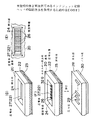
FIG. 3 is a view showing an ink jet recording head 40A according to the first embodiment of the present invention, and FIGS. 4 and 5 are views for explaining a method of manufacturing the ink jet recording head according to the first embodiment of the present invention. In this embodiment, a manufacturing method of the ink jet recording head 40A shown in FIG. 1 is shown. In each of the embodiments described below, an example in which a piezoelectric body is used as energy generating means for ejecting ink will be described, but a heating element may be used instead of the piezoelectric body.
[0055]
First, the configuration of the ink jet recording head 40A will be described with reference to FIG. In short, the ink jet recording head 40A includes a
As will be described later, the
[0056]
A
The
[0057]
The
[0058]
In the ink jet recording head 40A configured as described above, when a voltage is applied between the
The distortion generated in the
[0059]
In the above configuration, the ink jet recording head 40A according to the present embodiment is characterized in that the
Thus, by forming the
[0060]
In the present embodiment, the
[0061]
Subsequently, a manufacturing method of the ink jet recording head 40A having the above-described configuration will be described with reference to FIGS.
In order to manufacture the ink jet recording head 40A, the
[0062]
On this
[0063]
As described above, when the formation process of each of the
The formation position of the
[0064]
When the
[0065]
By performing the above separation step, the
[0066]
A specific method for forming the
[0067]
The
As described above, according to the present embodiment, the
[0068]
In addition, since no other bonding member such as an adhesive is interposed between the
[0069]
Further, in the above-described removal process, since the
[0070]
Further, in this embodiment, after the removal step is completed, a division step is performed, and the
[0071]
Further, as described above, in the present embodiment, the
[0072]
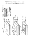
Next, an ink jet recording head 40B that is a second embodiment of the present invention and a method for manufacturing the same will be described with reference to FIGS.
FIG. 6 is a view showing an ink jet recording head 40B according to a second embodiment of the present invention, and FIGS. 7 and 8 are diagrams for explaining a method of manufacturing the ink jet recording head 40B according to the second embodiment of the present invention. FIG.
[0073]
In each of the embodiments described below, the same components as those of the ink jet recording head 40A according to the first embodiment described with reference to FIG. Similarly, in each embodiment described below, the description of the same process as the manufacturing process according to the first embodiment described with reference to FIGS. 4 and 5 is omitted.
[0074]
As shown in FIG. 6, the ink jet recording head 40 </ b> B according to the present embodiment has a configuration in which the
[0075]
Next, a method for manufacturing the ink jet recording head 40B having the above configuration will be described.
In the manufacturing method according to the first embodiment described above, the
[0076]
In this embodiment, the individual electrode forming process for forming the
When the
[0077]
As in this embodiment, the piezoelectric body 27 (piezoelectric layer 22) and the
As in the first embodiment, when a metal electrode layer (electrode layer 21) having no crystal lattice is interposed between the
[0078]
However, after forming the
[0079]
Next, an ink jet recording head 40C according to a third embodiment of the present invention and a method for manufacturing the same will be described with reference to FIGS.
FIG. 9 is a view showing an ink jet recording head 40C according to a third embodiment of the present invention, and FIGS. 10 and 11 illustrate a method for manufacturing the ink jet recording head 40C according to the third embodiment of the present invention. FIG.
[0080]
As shown in FIG. 9, in the ink jet recording head 40C according to the present embodiment, the piezoelectric body 27 (piezoelectric layer 22) is not divided, as in the ink jet recording head 40B according to the second embodiment. Only the
Next, a method for manufacturing the ink jet recording head 40C having the above configuration will be described. The manufacturing steps from FIG. 10A to FIG. 11D are the same as in the first embodiment. Therefore, the
[0081]
In the manufacturing method according to the present embodiment, the dividing step is performed after the removal step is completed, and only the
[0082]
As in this embodiment, the dividing step is performed after the removal step is completed, and only the
That is, in the method of dividing the dividing step before disposing the
[0083]
With this configuration, internal strains due to differences in lattice constants and the like are likely to occur in the
However, as in the present embodiment, the
[0084]
In addition, since the division position for dividing the
[0085]
However, by setting the division position of the
[0086]
Next, an ink jet recording head 40D that is a fourth embodiment of the present invention and a method for manufacturing the same will be described with reference to FIGS.
FIG. 12 is a view showing an ink jet recording head 40D according to a fourth embodiment of the present invention. FIGS. 13 and 14 are diagrams for explaining a method of manufacturing the ink jet recording head 40D according to the fourth embodiment of the present invention. FIG.
[0087]
As shown in FIG. 12, the ink jet recording head 40D according to the present embodiment is characterized in that the
In order to manufacture the ink jet recording head 40D having this configuration, first, as shown in FIG. 13A, a
[0088]
Subsequently, in this embodiment, a dividing step is performed before the
[0089]
Subsequently, as shown in FIG. 14E, the first
[0090]
Subsequently, the
When this masking process is completed, the substrate 10 is then etched with an acidic etching solution (for example, 50% phosphoric acid solution) to form the
[0091]
Subsequently, as shown in FIG. 14H, the second main body half 28B in which the
[0092]
As described above, when the second main body half body 28B is joined to the first main
[0093]
By joining the first and second body half halves 28A and 28B as described above, the first and second body half halves 28A and 28B cooperate to form the
As described above, in this embodiment, the first bonding step is performed before the removing step and the first main
[0094]
In addition, the formation of the
[0095]
Subsequently, a method for manufacturing an ink jet recording head according to a fifth embodiment of the present invention will be described with reference to FIGS. In the description of this embodiment, the description of the same steps as those of the ink jet recording head manufacturing method according to the fourth embodiment will be omitted.
Also in this embodiment, first, an electrode layer 21 (thickness 0.2 μm) made of Pt is formed by sputtering on a substrate 20 ([100] surface, thickness 300 μm) made of MgO. Then, alignment marks and
[0096]
Subsequently, a piezoelectric material is laminated to a thickness of about 3 μm by sputtering on the
[0097]
In this state, as shown in FIG. 15C, a gap is formed between the adjacent individual
Subsequently, sputtering using MgO as a target is performed to form a filler 36 between adjacent individual piezoelectric bodies 34 (filling step). At this time, the individual
[0098]
As described above, in this embodiment, the same material as that of the
[0099]
When the filling step is completed as described above, the vibrating
As in this embodiment, by performing the filling step and forming the filler 36 between the adjacent individual
[0100]
However, by disposing the filler 36 in the filling step, the surface of the surface formed by the individual
[0101]
When the
At this time, since the filler 36 is selected from the same material as that of the
[0102]
Thus, since each energy generation part 32D becomes an independent structure, the drivability of each energy generation part 32D can be improved, and low power consumption can be achieved.
Subsequently, the
[0103]
In the above-described embodiment, the filler 36 is made of the same material as that of the
[0104]
Furthermore, by using a material having elasticity and ink resistance as the filler 36, it is possible to prevent ink from leaking from the
In this case, the ink in the
[0105]
Subsequently, a method for manufacturing an ink jet recording head according to a sixth embodiment of the present invention will be described with reference to FIGS. In the description of this embodiment, the description of the same steps as those of the ink jet recording head manufacturing method according to the fourth and fifth embodiments will be omitted. The same applies to the description of each embodiment described below.
[0106]
Also in this embodiment, first, the
[0107]
In the fifth embodiment, the filler 36 is disposed after the individual
In this way, by forming the
[0108]
The ink jet recording head manufactured according to the present embodiment has a configuration in which a
[0109]
Subsequently, a method for manufacturing an ink jet recording head according to seventh and eighth embodiments of the present invention will be described with reference to FIGS.
In the seventh and eighth embodiments, the steps shown in FIGS. 19 (A) to 19 (F) and FIGS. 20 (A) to (F) are the same as those in the fifth embodiment shown in FIGS. Since it is the same as the process of F), the description is abbreviate | omitted.
[0110]
In each of the above-described embodiments (for example, the fifth embodiment), the second body half 28B is disposed after the removal step is performed and the
[0111]
Thus, when the opening
[0112]
In the seventh embodiment, the
[0113]
FIG. 21 shows an inkjet recording head 40E which is a fifth embodiment of the present invention. In FIG. 2, the same components as those of the ink jet recording head 40B according to the second embodiment described above with reference to FIG.
The ink jet recording head 40B according to the second embodiment described above is formed by laminating the
[0114]
And after joining and hardening a dry film on a board | plate material on the same conditions as demonstrated in 2nd Example, the edge used as a joining surface with the nozzle plate 38 is cut | disconnected with a dicing saw. In this embodiment, the
[0115]
The nozzle plate 38 was aligned and joined to this cut surface, thereby forming the ink jet recording head 40E shown in FIG. Even in the case of the side-shoot type ink jet recording head 40E as in this embodiment, a head with low power consumption and high yield can be easily manufactured.
[0116]
【The invention's effect】
As described above, according to the present invention, various effects described below can be realized. According to the first aspect of the present invention, since the thin and miniaturized ink discharge energy generating portion can be formed with high accuracy and high reliability, it is possible to achieve low power consumption and high resolution. Can be printed.
[0117]
[0118]
In addition, since a flat diaphragm can be disposed in the pressure chamber, it is possible to manufacture an ink jet recording head that has good adhesion between the piezoelectric body and the diaphragm and can be driven efficiently without variation. it can.
[0119]
In addition, since the first main body member half functioning as a reinforcing material exists on the back side of the opening forming position, it is possible to prevent the ink discharge energy generating portion from being damaged even after the opening is formed.
[0120]
Claims 5 According to the described invention, since the adjacent ink discharge energy generating portions are completely independent, the deformability (driveability) of the ink discharge energy generating portions is improved when a voltage is applied, thereby ensuring a reliable and responsive response. Ink can be discharged with good characteristics.
[0121]
[0122]
[0123]
Claims 11 According to the described invention, when the opening is formed in the removing step, the filler between the ink ejection energy generation units is also removed at the same time, so that each ink ejection energy generation unit has an independent configuration, and the ink ejection energy generation unit The driveability can be improved.
[0124]
Claims 13 According to the described invention, by using a material having elasticity and ink resistance as the filler, ink leakage from the pressure chamber can be prevented by the filler. Claims 14 According to the described invention, when the opening is formed in the removing step, the main body is bonded to the back side of the substrate, so that the ink formed on the substrate when the opening is formed It is possible to prevent the discharge energy generation unit from being damaged, and it is possible to improve yield and reliability.
[0125]
[Brief description of the drawings]
FIG. 1 is a main part configuration diagram of an example of a printer apparatus.
FIG. 2 is a partially cutaway perspective view of an ink jet recording head as an example of the prior art.
FIG. 3 is a partially cutaway perspective view of the ink jet recording head according to the first embodiment of the present invention.
FIG. 4 is a view for explaining the method of manufacturing the ink jet recording head according to the first embodiment of the invention (No. 1).
FIG. 5 is a drawing for explaining the method of manufacturing the ink jet recording head according to the first embodiment of the present invention (No. 2).
FIG. 6 is a partially cutaway perspective view of an ink jet recording head according to a second embodiment of the present invention.
FIG. 7 is a drawing for explaining a method of manufacturing an ink jet recording head according to a second embodiment of the invention (part 1).
FIG. 8 is a drawing for explaining the method of manufacturing the ink jet recording head according to the second embodiment of the present invention (No. 2).
FIG. 9 is a partially cutaway perspective view of an ink jet recording head according to a third embodiment of the present invention.
FIG. 10 is a diagram for explaining a method of manufacturing the ink jet recording head according to the third embodiment of the present invention (No. 1).
FIG. 11 is a drawing for explaining the method of manufacturing the ink jet recording head according to the third embodiment of the present invention (No. 2).
FIG. 12 is a partially cutaway perspective view of an ink jet recording head according to a fourth embodiment of the present invention.
FIG. 13 is a drawing for explaining the method of manufacturing the ink jet recording head according to the fourth embodiment of the present invention (No. 1).
FIG. 14 is a drawing for explaining the method of manufacturing the ink jet recording head according to the fourth embodiment of the present invention (# 2).
FIG. 15 is a drawing for explaining a method for producing an ink jet recording head according to a fifth embodiment of the present invention (# 1).
FIG. 16 is a drawing for explaining the method of manufacturing the ink jet recording head according to the fifth embodiment of the present invention (# 2).
FIG. 17 is a drawing for explaining a method for producing an ink jet recording head according to a sixth embodiment of the present invention (# 1).
FIG. 18 is a drawing for explaining the method of manufacturing the ink jet recording head according to the sixth embodiment of the present invention (No. 2).
FIG. 19 is a view for explaining the method of manufacturing the ink jet recording head according to the seventh embodiment of the invention.
FIG. 20 is a view for explaining the method of manufacturing the ink jet recording head according to the eighth embodiment of the present invention.
FIG. 21 is a partially cutaway perspective view of an ink jet recording head according to a fifth embodiment of the present invention.
[Explanation of symbols]
20 substrates
21 Electrode layer
22 Piezoelectric layer
23 Diaphragm
24 opening
25 Pressure chamber position
26 Individual electrodes
27 Piezoelectric material
28 Body
28A First body half
28B Second body half
29 Pressure chamber
29A first pressure chamber half
29B second pressure chamber half
30,38 Nozzle plate
31,39 nozzles
32A to 32E Energy generator
34 Individual piezoelectric body
35 frame
36 Filler
37 Diaphragm film
40A-40E inkjet recording head
Claims (19)
振動可能な材料により形成されており、前記圧力室の一の壁面を構成する振動板と、
前記圧力室と対応する前記振動板上に配設されており、前記振動板を変形することにより前記圧力室内のインクを前記ノズルから吐出させるインク吐出エネルギー発生部とを有するインクジェット記録ヘッドにおいて、
薄膜形成技術を用いて、基板上に、前記インク吐出エネルギー発生部を構成する個別電極層及びエネルギー発生層を形成し、さらにその上に振動板を形成するとともに、
前記基板の少なくとも前記インク吐出エネルギー発生部の変形領域に対応する領域を除去することにより形成された、前記基板から前記インク吐出エネルギー発生部を露出させるための開口部を有することを特徴とするインクジェット記録ヘッド。A main body portion provided corresponding to a nozzle for ejecting ink, and formed with a plurality of pressure chambers filled with ink;
A vibration plate formed of a material capable of vibration, and constituting one wall surface of the pressure chamber;
An ink jet recording head that is disposed on the diaphragm corresponding to the pressure chamber, and has an ink ejection energy generation unit that ejects ink in the pressure chamber from the nozzle by deforming the diaphragm;
Using a thin film forming technique, on the substrate, the individual electrode layer and the energy generation layer constituting the ink discharge energy generation unit are formed, and further the vibration plate is formed thereon,
An ink jet having an opening for exposing the ink discharge energy generating portion from the substrate, formed by removing at least a region corresponding to a deformation region of the ink discharge energy generating portion of the substrate. Recording head.
前記基板の少なくとも前記インク吐出エネルギー発生部の変形領域に対応する領域を除去して開口部を形成することにより、前記基板から前記インク吐出エネルギー発生部を露出させる除去工程と、
予めインクを吐出するための圧力室が形成されてなる本体部材を前記振動板に接合する接合工程と、
前記圧力室と対応する位置にインクを吐出するノズル孔が形成されると共に、前記本体部材にノズル板を配設するノズル板配設工程と、
を有することを特徴とするインクジェット記録ヘッドの製造方法。And energy generating part forming step of forming an ink discharge energy generating unit by the substrate the individual electrode layer using a thin film formation technology, energy generating layer are sequentially formed diaphragm,
A removal step of exposing the ink discharge energy generating portion from the substrate by removing an area corresponding to a deformation region of the ink discharge energy generating portion of the substrate to form an opening;
A bonding step of bonding a body member pressure chamber is formed for discharging beforehand ink to said diaphragm,
A nozzle hole for discharging ink at a position corresponding to the pressure chamber, and a nozzle plate disposing step of disposing a nozzle plate on the main body member;
An ink jet recording head manufacturing method comprising:
前記接合工程は、
前記エネルギー発生部形成工程と前記除去工程との間に実施され、前記振動板上に、予めインクを吐出するための第1の圧力室半体が形成されてなる第1の本体部材半体を接合する第1の接合工程と、
前記除去工程の終了後、予めインクを吐出するための第2の圧力室半体が形成されてなる第2の本体部材半体を前記第1の本体部材半体に接合する第2の接合工程とよりなることを特徴とするインクジェット記録ヘッドの製造方法。In the manufacturing method of the ink-jet recording head according to claim 2 ,
The joining step includes
Wherein is performed between the energy generating portion forming step and the removing step, on the vibrating plate, the first body member halves comprising a first pressure chamber half for discharging a pre-ink form A first joining step for joining;
After the removal step, a second joining step of joining a second body member half formed with a second pressure chamber half for discharging ink in advance to the first body member half. An ink jet recording head manufacturing method comprising:
前記エネルギー発生部形成工程は、
前記個別電極層を形成した後で、かつ前記エネルギー発生層を形成する前に、前記インク吐出エネルギー発生部の形成位置で前記個別電極層を分割し、個別電極を形成する分割工程を有することを特徴とするインクジェット記録ヘッドの製造方法。In the manufacturing method of the inkjet recording head of Claim 2 or Claim 3 ,
The energy generating part forming step includes
After the formation of the individual electrode layer and before the formation of the energy generation layer, the method includes a division step of dividing the individual electrode layer at the formation position of the ink discharge energy generation unit to form individual electrodes. A method of manufacturing an ink jet recording head.
前記エネルギー発生部形成工程は、
前記除去工程を終了した後に、前記開口部に露出した前記個別電極層と前記エネルギー発生層とを前記インク吐出エネルギー発生部の形成位置において共に分割し、個別電極を形成する分割工程を有することを特徴とするインクジェット記録ヘッドの製造方法。In the manufacturing method of the ink-jet recording head according to claim 2 or 3 ,
The energy generating part forming step includes
After the removal step, the individual electrode layer exposed to the opening and the energy generation layer are divided together at the formation position of the ink discharge energy generation unit to have a division step of forming individual electrodes. A method of manufacturing an ink jet recording head.
前記エネルギー発生部形成工程は、
前記除去工程を終了した後に、前記開口部に露出した前記個別電極層のみを前記インク吐出エネルギー発生部の形成位置において分割し、個別電極を形成する分割工程を有することを特徴とするインクジェット記録ヘッドの製造方法。In the manufacturing method of the ink-jet recording head according to claim 2 or 3 ,
The energy generating part forming step includes
An ink jet recording head comprising: a dividing step of dividing only the individual electrode layer exposed to the opening after the removing step at a position where the ink discharge energy generating portion is formed to form individual electrodes. Manufacturing method.
前記エネルギー発生部形成工程で、
複数の前記圧力室にまたがるよう前記インク吐出エネルギー発生部を形成することを特徴とするインクジェット記録ヘッドの製造方法。In the manufacturing method of the ink-jet recording head according to claim 6 ,
In the energy generation part forming step,
A method of manufacturing an ink jet recording head, wherein the ink discharge energy generating portion is formed so as to span a plurality of the pressure chambers.
前記基板の少なくとも前記インク吐出エネルギー発生部の変形領域に対応する領域を除去して開口部を形成することにより、前記基板から前記インク吐出エネルギー発生部を露出させる除去工程と、
該除去工程の終了後、前記開口部を介して前記インク吐出エネルギー発生部と対応する位置に個別電極を形成する個別電極形成工程と、
予めインクを吐出するための圧力室が形成されてなる本体部材を前記振動板に接合する接合工程とを有することを特徴とするインクジェット記録ヘッドの製造方法。An energy generating part forming step of sequentially forming an energy generating layer and a vibration plate as an ink discharge energy generating part on a substrate using a thin film forming technique;
A removal step of exposing the ink discharge energy generating portion from the substrate by removing an area corresponding to a deformation region of the ink discharge energy generating portion of the substrate to form an opening;
An individual electrode forming step of forming an individual electrode at a position corresponding to the ink ejection energy generation unit through the opening after the removal step;
A method of manufacturing an ink jet recording head, comprising: a bonding step of bonding a main body member, in which a pressure chamber for discharging ink in advance is formed, to the diaphragm.
前記分割工程で前記分割処理を行う分割位置を、隣り合う前記圧力室の間位置に設定したことを特徴とするインクジェット記録ヘッドの製造方法。In the manufacturing method of the ink-jet recording head according to any one of claims 4 to 7 ,
A method for manufacturing an ink jet recording head, wherein a dividing position for performing the dividing process in the dividing step is set to a position between adjacent pressure chambers.
前記基板の少なくとも前記インク吐出エネルギー発生部の変形領域に対応する領域を除去して開口部を形成することにより、前記基板から前記インク吐出エネルギー発生部を露出させる除去工程と、
予めインクを吐出するための圧力室が形成されてなる本体部材を前記振動板に接合する接合工程とを有することを特徴とするインクジェット記録ヘッドの製造方法。An individual electrode forming step of forming an individual electrode layer on a substrate using a thin film forming technique, an individual energy generating layer forming step of forming an individual energy generating layer on at least the individual electrode layer, and the individual energy generating layer forming step A filling step of disposing a filler in a gap portion between the individual energy generation layers formed in the step, and a vibration layer forming step of forming a diaphragm on the individual energy generation layer and the filler after the filling step is completed. An energy generating part forming step of forming an ink discharge energy generating part by performing
A removal step of exposing the ink discharge energy generating portion from the substrate by removing an area corresponding to a deformation region of the ink discharge energy generating portion of the substrate to form an opening;
A method of manufacturing an ink jet recording head, comprising: a bonding step of bonding a main body member, in which a pressure chamber for discharging ink in advance is formed, to the diaphragm.
前記充填材として、前記基板と同一材料を用いたことを特徴とするインクジェット記録ヘッドの製造方法。In the manufacturing method of the ink-jet recording head according to claim 10 ,
A method of manufacturing an ink jet recording head, wherein the same material as the substrate is used as the filler.
前記充填材として、ヤング率が前記エネルギー発生層の材料よりも小さく、90GPa以下であるものを用いたことを特徴とするインクジェット記録ヘッドの製造方法。In the manufacturing method of the ink-jet recording head according to claim 10 ,
A method of manufacturing an ink jet recording head, wherein the filler has a Young's modulus smaller than that of the material of the energy generation layer and is 90 GPa or less.
前記充填材として、弾性及び耐インク性のある材料を用いたことを特徴とするインクジェット記録ヘッドの製造方法。In the manufacturing method of the ink-jet recording head according to any one of claims 10 to 12 ,
An ink jet recording head manufacturing method using an elastic and ink-resistant material as the filler.
前記接合工程を実施した後に、前記除去工程を実施することを特徴とするインクジェット記録ヘッドの製造方法。In the manufacturing method of the ink-jet recording head according to claim 2 ,
A method of manufacturing an ink jet recording head, wherein the removing step is performed after the joining step.
前記ノズル板配設工程を前記接合工程の前に実施することを特徴とするインクジェット記録ヘッドの製造方法。In the manufacturing method of the ink-jet recording head according to any one of claims 2 to 14 ,
A method of manufacturing an ink jet recording head, wherein the nozzle plate disposing step is performed before the joining step.
前記ノズル板配設工程を前記接合工程の後に実施することを特徴とするインクジェット記録ヘッドの製造方法。In the manufacturing method of the ink-jet recording head according to any one of claims 2 to 14 ,
A method of manufacturing an ink jet recording head, wherein the nozzle plate disposing step is performed after the joining step.
更に、前記除去工程を実施した後に、前記基板に形成した開口部に熱伝達性の高い材料を配設する放熱部形成工程を実施することを特徴とするインクジェット記録ヘッドの製造方法。In the manufacturing method of the ink-jet recording head according to any one of claims 2 to 16 ,
Furthermore, after performing the said removal process, the manufacturing method of the inkjet recording head characterized by implementing the thermal radiation part formation process which arrange | positions a material with high heat transfer property to the opening part formed in the said board | substrate.
前記圧電体を基板上に薄膜形成技術を用いて成長させる成長工程と、
前記圧電体の変形する部分の周囲の基板を残し、前記圧電体の変形する部分の基板を除去し、前記基板から前記インク吐出エネルギー発生部を露出させるための開口部を形成する除去工程とにより形成された圧電体を用いたことを特徴とするインクジェット記録ヘッド。In an ink jet recording head comprising a pressure chamber and a piezoelectric body, deforming the piezoelectric body by an electrical signal, and discharging ink in the pressure chamber.
A growth step of growing the piezoelectric body on a substrate using a thin film forming technique;
A removing step of leaving a substrate around the deformable portion of the piezoelectric body, removing the deformable portion of the piezoelectric body, and forming an opening for exposing the ink discharge energy generating portion from the substrate; An ink jet recording head using a formed piezoelectric body.
前記圧電体を基板上に薄膜形成技術を用いて成長させる成長工程と、
前記圧電体の変形する部分の周囲の基板を残し、前記圧電体の変形する部分の基板を除去し、前記基板から前記インク吐出エネルギー発生部を露出させるための開口部を形成する除去工程とにより形成された圧電体を用いたインクジェット記録ヘッドを有することを特徴とするプリンタ装置。In a printer apparatus using an ink jet recording head that includes a pressure chamber and a piezoelectric body, deforms the piezoelectric body by an electric signal, and discharges ink in the pressure chamber.
A growth step of growing the piezoelectric body on a substrate using a thin film forming technique;
A removing step of leaving a substrate around the deformable portion of the piezoelectric body, removing the deformable portion of the piezoelectric body, and forming an opening for exposing the ink discharge energy generating portion from the substrate; A printer apparatus comprising an ink jet recording head using a formed piezoelectric body.
Priority Applications (4)
| Application Number | Priority Date | Filing Date | Title |
|---|---|---|---|
| JP29791998A JP3823567B2 (en) | 1998-10-20 | 1998-10-20 | Ink jet recording head, manufacturing method thereof, and printer apparatus |
| PCT/JP1999/001570 WO2000023277A1 (en) | 1998-10-20 | 1999-03-26 | Ink jet recording head, its manufacturing method, and printer device |
| DE19983673T DE19983673B4 (en) | 1998-10-20 | 1999-03-26 | Ink jet recording head manufacturing method |
| US09/807,430 US6623110B2 (en) | 1998-10-20 | 2001-04-20 | Ink jet recording head and production methods therefor and printer apparatus therewith |
Applications Claiming Priority (1)
| Application Number | Priority Date | Filing Date | Title |
|---|---|---|---|
| JP29791998A JP3823567B2 (en) | 1998-10-20 | 1998-10-20 | Ink jet recording head, manufacturing method thereof, and printer apparatus |
Publications (3)
| Publication Number | Publication Date |
|---|---|
| JP2000117990A JP2000117990A (en) | 2000-04-25 |
| JP2000117990A5 JP2000117990A5 (en) | 2005-12-02 |
| JP3823567B2 true JP3823567B2 (en) | 2006-09-20 |
Family
ID=17852799
Family Applications (1)
| Application Number | Title | Priority Date | Filing Date |
|---|---|---|---|
| JP29791998A Expired - Fee Related JP3823567B2 (en) | 1998-10-20 | 1998-10-20 | Ink jet recording head, manufacturing method thereof, and printer apparatus |
Country Status (4)
| Country | Link |
|---|---|
| US (1) | US6623110B2 (en) |
| JP (1) | JP3823567B2 (en) |
| DE (1) | DE19983673B4 (en) |
| WO (1) | WO2000023277A1 (en) |
Families Citing this family (10)
| Publication number | Priority date | Publication date | Assignee | Title |
|---|---|---|---|---|
| DE69931526T2 (en) | 1999-12-10 | 2007-04-26 | Fuji Photo Film Co., Ltd., Minami-Ashigara | INK JET PRINT HEAD, METHOD FOR PRODUCING PRINT HEADS AND PRINTER |
| JP4554135B2 (en) | 1999-12-10 | 2010-09-29 | 富士フイルム株式会社 | Inkjet head and printing apparatus |
| KR100566846B1 (en) | 1999-12-24 | 2006-04-03 | 후지 샤신 필름 가부시기가이샤 | Method of manufacturing ink-jet record head |
| KR100567294B1 (en) | 1999-12-24 | 2006-04-04 | 후지 샤신 필름 가부시기가이샤 | Ink-jet record head and method of manufacture thereof |
| US6886924B2 (en) * | 2002-09-30 | 2005-05-03 | Spectra, Inc. | Droplet ejection device |
| JP3820589B2 (en) * | 2003-09-26 | 2006-09-13 | 富士写真フイルム株式会社 | Liquid discharge head, manufacturing method thereof, and ink jet recording apparatus |
| US8042913B2 (en) * | 2006-09-14 | 2011-10-25 | Hewlett-Packard Development Company, L.P. | Fluid ejection device with deflective flexible membrane |
| US7651204B2 (en) * | 2006-09-14 | 2010-01-26 | Hewlett-Packard Development Company, L.P. | Fluid ejection device |
| JP5382905B2 (en) * | 2008-03-10 | 2014-01-08 | 富士フイルム株式会社 | Method for manufacturing piezoelectric element and method for manufacturing liquid discharge head |
| EP2974867B1 (en) * | 2013-03-15 | 2023-12-06 | Konica Minolta, Inc. | Inkjet head, method for manufacturing same, and inkjet printer |
Family Cites Families (8)
| Publication number | Priority date | Publication date | Assignee | Title |
|---|---|---|---|---|
| JPS63128948A (en) * | 1986-11-19 | 1988-06-01 | Sharp Corp | Ink jet head |
| US4825227A (en) * | 1988-02-29 | 1989-04-25 | Spectra, Inc. | Shear mode transducer for ink jet systems |
| JP3144949B2 (en) * | 1992-05-27 | 2001-03-12 | 日本碍子株式会社 | Piezoelectric / electrostrictive actuator |
| US5907338A (en) * | 1995-01-13 | 1999-05-25 | Burr; Ronald F. | High-performance ink jet print head |
| JP3503386B2 (en) * | 1996-01-26 | 2004-03-02 | セイコーエプソン株式会社 | Ink jet recording head and method of manufacturing the same |
| JPH09300608A (en) * | 1996-05-09 | 1997-11-25 | Minolta Co Ltd | Ink-jet recording head |
| JPH10202874A (en) * | 1997-01-24 | 1998-08-04 | Seiko Epson Corp | Ink jet printing head and its production |
| JP3666177B2 (en) * | 1997-04-14 | 2005-06-29 | 松下電器産業株式会社 | Inkjet recording device |
-
1998
- 1998-10-20 JP JP29791998A patent/JP3823567B2/en not_active Expired - Fee Related
-
1999
- 1999-03-26 DE DE19983673T patent/DE19983673B4/en not_active Expired - Fee Related
- 1999-03-26 WO PCT/JP1999/001570 patent/WO2000023277A1/en active Application Filing
-
2001
- 2001-04-20 US US09/807,430 patent/US6623110B2/en not_active Expired - Lifetime
Also Published As
| Publication number | Publication date |
|---|---|
| US20010022602A1 (en) | 2001-09-20 |
| WO2000023277A1 (en) | 2000-04-27 |
| DE19983673B4 (en) | 2008-02-14 |
| US6623110B2 (en) | 2003-09-23 |
| DE19983673T1 (en) | 2002-02-14 |
| JP2000117990A (en) | 2000-04-25 |
Similar Documents
| Publication | Publication Date | Title |
|---|---|---|
| US7159971B2 (en) | Multi-nozzle ink jet head | |
| US20040085411A1 (en) | Ink jet recording head and method of producing a plate member for an ink jet recording head | |
| JP3823567B2 (en) | Ink jet recording head, manufacturing method thereof, and printer apparatus | |
| US6109738A (en) | Ink jet print head and a method of manufacturing the same | |
| WO1999003682A1 (en) | Inkjet recording head, method of manufacturing the same, and inkjet recorder | |
| US6350019B1 (en) | Ink jet head and ink jet printer | |
| JPH03297653A (en) | Ink jet head | |
| JP3291999B2 (en) | Ink jet print head | |
| JP3522163B2 (en) | Inkjet recording head and inkjet recording apparatus | |
| JP4508595B2 (en) | Liquid ejecting head, manufacturing method thereof, and liquid ejecting apparatus | |
| JP4385653B2 (en) | Liquid ejecting head and manufacturing method thereof | |
| JP2001260348A (en) | Ink jet recording head and ink jet recorder | |
| JP3603931B2 (en) | Ink jet recording head and ink jet recording apparatus | |
| JP3330757B2 (en) | Ink jet head and method of manufacturing the same | |
| JP3185434B2 (en) | Inkjet print head | |
| JP2011224785A (en) | Method for manufacturing of liquid jet head | |
| JP3879117B2 (en) | Method for manufacturing ink jet recording head | |
| JP4483682B2 (en) | Nozzle plate processing method | |
| JP2000006398A (en) | Ink jet recording head, manufacture thereof, and ink jet recorder | |
| JP4461783B2 (en) | Method for manufacturing liquid jet head | |
| JP2004268397A (en) | Manufacturing method for liquid injection head, and joining apparatus | |
| JP2007196431A (en) | Liquid droplet delivering head, and method for manufacturing liquid droplet delivering head | |
| JPH11309858A (en) | Ink jet recording head, driving method therefor and ink jet recorder | |
| JP2000085133A (en) | Manufacture of ink jet type recording head | |
| JP2005131948A (en) | Head module, liquid ejection head, liquid ejector, process for manufacturing head module, and process for manufacturing liquid ejection head |
Legal Events
| Date | Code | Title | Description |
|---|---|---|---|
| A711 | Notification of change in applicant |
Free format text: JAPANESE INTERMEDIATE CODE: A711 Effective date: 20040611 |
|
| A521 | Written amendment |
Free format text: JAPANESE INTERMEDIATE CODE: A523 Effective date: 20051018 |
|
| A621 | Written request for application examination |
Free format text: JAPANESE INTERMEDIATE CODE: A621 Effective date: 20051018 |
|
| A131 | Notification of reasons for refusal |
Free format text: JAPANESE INTERMEDIATE CODE: A131 Effective date: 20060317 |
|
| A521 | Written amendment |
Free format text: JAPANESE INTERMEDIATE CODE: A523 Effective date: 20060516 |
|
| TRDD | Decision of grant or rejection written | ||
| A01 | Written decision to grant a patent or to grant a registration (utility model) |
Free format text: JAPANESE INTERMEDIATE CODE: A01 Effective date: 20060606 |
|
| A61 | First payment of annual fees (during grant procedure) |
Free format text: JAPANESE INTERMEDIATE CODE: A61 Effective date: 20060619 |
|
| R150 | Certificate of patent or registration of utility model |
Free format text: JAPANESE INTERMEDIATE CODE: R150 |
|
| FPAY | Renewal fee payment (event date is renewal date of database) |
Free format text: PAYMENT UNTIL: 20090707 Year of fee payment: 3 |
|
| S111 | Request for change of ownership or part of ownership |
Free format text: JAPANESE INTERMEDIATE CODE: R313111 |
|
| FPAY | Renewal fee payment (event date is renewal date of database) |
Free format text: PAYMENT UNTIL: 20090707 Year of fee payment: 3 |
|
| R350 | Written notification of registration of transfer |
Free format text: JAPANESE INTERMEDIATE CODE: R350 |
|
| FPAY | Renewal fee payment (event date is renewal date of database) |
Free format text: PAYMENT UNTIL: 20090707 Year of fee payment: 3 |
|
| FPAY | Renewal fee payment (event date is renewal date of database) |
Free format text: PAYMENT UNTIL: 20100707 Year of fee payment: 4 |
|
| FPAY | Renewal fee payment (event date is renewal date of database) |
Free format text: PAYMENT UNTIL: 20110707 Year of fee payment: 5 |
|
| FPAY | Renewal fee payment (event date is renewal date of database) |
Free format text: PAYMENT UNTIL: 20110707 Year of fee payment: 5 |
|
| FPAY | Renewal fee payment (event date is renewal date of database) |
Free format text: PAYMENT UNTIL: 20120707 Year of fee payment: 6 |
|
| FPAY | Renewal fee payment (event date is renewal date of database) |
Free format text: PAYMENT UNTIL: 20120707 Year of fee payment: 6 |
|
| FPAY | Renewal fee payment (event date is renewal date of database) |
Free format text: PAYMENT UNTIL: 20130707 Year of fee payment: 7 |
|
| R250 | Receipt of annual fees |
Free format text: JAPANESE INTERMEDIATE CODE: R250 |
|
| R250 | Receipt of annual fees |
Free format text: JAPANESE INTERMEDIATE CODE: R250 |
|
| R250 | Receipt of annual fees |
Free format text: JAPANESE INTERMEDIATE CODE: R250 |
|
| LAPS | Cancellation because of no payment of annual fees |