JP3813134B2 - Ball forming apparatus in wire bonding apparatus - Google Patents
Ball forming apparatus in wire bonding apparatus Download PDFInfo
- Publication number
- JP3813134B2 JP3813134B2 JP2003111616A JP2003111616A JP3813134B2 JP 3813134 B2 JP3813134 B2 JP 3813134B2 JP 2003111616 A JP2003111616 A JP 2003111616A JP 2003111616 A JP2003111616 A JP 2003111616A JP 3813134 B2 JP3813134 B2 JP 3813134B2
- Authority
- JP
- Japan
- Prior art keywords
- circuit
- voltage
- current
- command pulse
- transformer
- Prior art date
- Legal status (The legal status is an assumption and is not a legal conclusion. Google has not performed a legal analysis and makes no representation as to the accuracy of the status listed.)
- Expired - Lifetime
Links
Images


Classifications
-
- H—ELECTRICITY
- H01—ELECTRIC ELEMENTS
- H01L—SEMICONDUCTOR DEVICES NOT COVERED BY CLASS H10
- H01L24/00—Arrangements for connecting or disconnecting semiconductor or solid-state bodies; Methods or apparatus related thereto
- H01L24/74—Apparatus for manufacturing arrangements for connecting or disconnecting semiconductor or solid-state bodies
- H01L24/78—Apparatus for connecting with wire connectors
-
- H—ELECTRICITY
- H01—ELECTRIC ELEMENTS
- H01L—SEMICONDUCTOR DEVICES NOT COVERED BY CLASS H10
- H01L21/00—Processes or apparatus adapted for the manufacture or treatment of semiconductor or solid state devices or of parts thereof
- H01L21/02—Manufacture or treatment of semiconductor devices or of parts thereof
- H01L21/04—Manufacture or treatment of semiconductor devices or of parts thereof the devices having at least one potential-jump barrier or surface barrier, e.g. PN junction, depletion layer or carrier concentration layer
- H01L21/50—Assembly of semiconductor devices using processes or apparatus not provided for in a single one of the subgroups H01L21/06 - H01L21/326, e.g. sealing of a cap to a base of a container
- H01L21/60—Attaching or detaching leads or other conductive members, to be used for carrying current to or from the device in operation
-
- H—ELECTRICITY
- H01—ELECTRIC ELEMENTS
- H01L—SEMICONDUCTOR DEVICES NOT COVERED BY CLASS H10
- H01L2224/00—Indexing scheme for arrangements for connecting or disconnecting semiconductor or solid-state bodies and methods related thereto as covered by H01L24/00
- H01L2224/74—Apparatus for manufacturing arrangements for connecting or disconnecting semiconductor or solid-state bodies and for methods related thereto
- H01L2224/78—Apparatus for connecting with wire connectors
-
- H—ELECTRICITY
- H01—ELECTRIC ELEMENTS
- H01L—SEMICONDUCTOR DEVICES NOT COVERED BY CLASS H10
- H01L2224/00—Indexing scheme for arrangements for connecting or disconnecting semiconductor or solid-state bodies and methods related thereto as covered by H01L24/00
- H01L2224/80—Methods for connecting semiconductor or other solid state bodies using means for bonding being attached to, or being formed on, the surface to be connected
- H01L2224/85—Methods for connecting semiconductor or other solid state bodies using means for bonding being attached to, or being formed on, the surface to be connected using a wire connector
- H01L2224/85009—Pre-treatment of the connector or the bonding area
- H01L2224/8503—Reshaping, e.g. forming the ball or the wedge of the wire connector
-
- H—ELECTRICITY
- H01—ELECTRIC ELEMENTS
- H01L—SEMICONDUCTOR DEVICES NOT COVERED BY CLASS H10
- H01L2924/00—Indexing scheme for arrangements or methods for connecting or disconnecting semiconductor or solid-state bodies as covered by H01L24/00
- H01L2924/0001—Technical content checked by a classifier
- H01L2924/00014—Technical content checked by a classifier the subject-matter covered by the group, the symbol of which is combined with the symbol of this group, being disclosed without further technical details
-
- H—ELECTRICITY
- H01—ELECTRIC ELEMENTS
- H01L—SEMICONDUCTOR DEVICES NOT COVERED BY CLASS H10
- H01L2924/00—Indexing scheme for arrangements or methods for connecting or disconnecting semiconductor or solid-state bodies as covered by H01L24/00
- H01L2924/01—Chemical elements
- H01L2924/01005—Boron [B]
-
- H—ELECTRICITY
- H01—ELECTRIC ELEMENTS
- H01L—SEMICONDUCTOR DEVICES NOT COVERED BY CLASS H10
- H01L2924/00—Indexing scheme for arrangements or methods for connecting or disconnecting semiconductor or solid-state bodies as covered by H01L24/00
- H01L2924/01—Chemical elements
- H01L2924/01006—Carbon [C]
-
- H—ELECTRICITY
- H01—ELECTRIC ELEMENTS
- H01L—SEMICONDUCTOR DEVICES NOT COVERED BY CLASS H10
- H01L2924/00—Indexing scheme for arrangements or methods for connecting or disconnecting semiconductor or solid-state bodies as covered by H01L24/00
- H01L2924/01—Chemical elements
- H01L2924/01033—Arsenic [As]
Description
【0001】
【発明の属する技術分野】
本発明は、ワイヤボンディング装置におけるボール形成装置に関する。
【0002】
【従来の技術】
従来のワイヤボンディング装置におけるボール形成装置は、商用電源を変圧整流する変圧整流回路と、直列接続され自励パルス発振器の出力によりオンオフするトランジスタ素子と、このトランジスタ素子がオンオフした出力から高電圧出力を得るパルス変圧器と、前記自励パルス発振器を内蔵し、発振パルス幅を連続的に制御するように高電圧出力端子(放電電極)と接地(ワイヤ)間の電気信号が帰還されるパルス変調波発生回路とを備えている。例えば、特許文献1及び2参照。
【0003】
【特許文献1】
特開平5−235078号公報
【特許文献2】
特開平7−183322号公報
【0004】
【発明が解決しようとする課題】
上記従来技術は、トランジスタ素子を繰り返しオンオフさせてパルス変圧器より高電圧出力を得るので、放電電極とワイヤ先端間には、図3(a)(b)に示すように、ギザギザの放電電圧及び放電電流が出力される。このため、放電を停止させる位置が山部又は谷部になり、形成されるボール径が安定しなくバラツキが生じる。即ち、放電毎の放電時間と放電電流の安定性が悪い。特に、例えばワイヤ径の1.5倍以下のボール径を形成する場合には、その影響が顕著に表れる。
【0005】
本発明の課題は、均一なボール径を安定して形成することができるワイヤボンディング装置におけるボール形成装置を提供することにある。
【0006】
【課題を解決するための手段】
上記課題を解決するための本発明の請求項1は、キャピラリに挿通されたワイヤの先端と放電電極間に高電圧を印加して放電を行い、ワイヤの先端にボールを形成するワイヤボンディング装置におけるボール形成装置において、電圧指令パルスを出力する電圧指令パルス回路と、電流指令パルスを予め設定された時間出力する電流指令パルス回路と、前記電圧指令パルスが入力されて昇圧する昇圧トランスと、この昇圧トランスの放電電圧をフィードバックして定電圧制御する定電圧回路と、放電時の電流を検出した時に前記電流指令パルスを前記昇圧トランスに入力するように切り替えるスイッチ回路と、前記放電電流を前記電流指令パルス時間出力する定電流回路とを備えたことを特徴とする。
【0007】
上記課題を解決するための本発明の請求項2は、上記請求項1において、前記昇圧トランスは、定電圧機能及び定電流機能の両機能を有するリニア出力型トランスであることを特徴とする。
【0008】
【発明の実施の形態】
本発明のワイヤボンディング装置におけるボール形成装置の一実施の形態を図1及び図2により説明する。図1に示すように、キャピラリ1に挿通されたワイヤ2の先端にボール2aを形成するための放電電極3は、昇圧トランス4の出力側の一方の端子に接続されている。昇圧トランス4の出力側の他方の端子は、電流検出抵抗R1を有する電流検出回路5に接続されている。昇圧トランス4の入力側の一方の端子には、一定の電圧Vcc、例えばDC20Vの電圧が印加されており、昇圧トランス4の入力側の他方の端子には、後記する回路を介して電圧指令パルス回路10及び電流指令パルス回路11が接続されている。
【0009】
電圧指令パルス回路10は、昇圧トランス4より高電圧を発生させるための電圧指令パルス10aを出力する。電流指令パルス回路11は、昇圧トランス4より一定の定電流が出力した後に、この定電流を一定時間維持するための電流指令パルス11aを出力する。この電流指令パルス11aの出力時間、即ちパルス幅は、パルス幅設定回路12により設定される。パルス幅の設定は、予めワイヤ2の径、ワイヤ2の材質、形成するボール径2a等によって予め実験により設定する。
【0010】
電圧指令パルス回路10は、定電圧回路13の+側に接続され、定電圧回路13の−側には、前記放電電極3に印加された高電圧を検出する放電電圧検出回路14の分圧抵抗R2と分圧抵抗R3で分圧された分圧電圧が入力される。電流指令パルス回路11は、定電流回路15の+側に接続され、定電流回路15の−側には、前記電流検出回路5で検出された電流が入力される。
【0011】
定電圧回路13の出力端子はスイッチ回路20の一方の入力端子20aに接続され、定電流回路15の入力端子はスイッチ回路20の他方の入力端子20bに接続されている。スイッチ回路20の出力端子20cは、ドライバ21を介して前記昇圧トランス4の入力側の他方の端子に接続されている。スイッチ回路20の切り換えは、放電電流検出回路22の出力によって切り換えられる。
【0012】
放電電流検出回路22の+側には、放電電流検出レベル設定回路23が接続されており、放電電流検出レベル設定回路23は、予め設定された放電電流を出力する。放電電流検出回路22の−側には、電流検出回路5で検出された電流が入力される。前記スイッチ回路20は、ボール形成前は入力端子20aが出力端子20cに接続されており、放電電流検出回路22の出力によって入力端子20bが出力端子20cに接続される。
【0013】
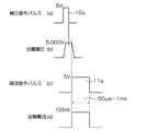
次に作用について説明する。ワイヤ2の先端にボール2aを形成する時は、電圧指令パルス回路10より図2(a)に示す例えば5Vの電圧指令パルス10aが定電圧回路13に入力される。これにより、定電圧回路13の出力は、スイッチ回路20の入力端子20aと出力端子20cよりドライバ21を通して昇圧トランス4に入力され、昇圧トランス4によって昇圧される。この昇圧された高電圧が放電電圧検出回路14の分圧抵抗R2と分圧抵抗R3で分圧された電圧は、定電圧回路13の−側にフィードバックされて定電圧制御して昇圧トランス4により放電電極3とワイヤ2の先端に図2(b)に示す例えば5,000Vの高電圧を印加する。
【0014】
前記高電圧の印加によって放電電極3とワイヤ2の先端との絶縁が破壊して電流検出回路5に電流が流れる。この電流検出回路5に流れる電流は、放電電流検出回路22の−側に入力され、この電流が放電電流検出レベル設定回路23により予め設定された設定電流になると、即座に放電電流検出回路22より出力信号がスイッチ回路20に入力され、スイッチ回路20の入力端子20bが出力端子20cに接続させる。これにより、電流指令パルス回路11より定電流回路15に入力されている図2(c)に示す電流指令パルス11aが一定時間、スイッチ回路20、ドライバ21を通して昇圧トランス4に入力される。そこで、放電電極3よりワイヤ2に定電流が流れ、ワイヤ2の先端に所定のボール2aが形成される。
【0015】
このように、電圧指令パルス10aを昇圧トランス4に入力し、昇圧トランス4の放電電圧をフィードバックして定電圧回路13で定電圧制御された高電圧を放電電極3とワイヤ2の先端間に印加する。そして、放電電極3とワイヤ2の先端との絶縁が破壊して設定電流が流れると、即座に電流指令パルス11aが昇圧トランス4に入力して一定時間定電流が放電電極3よりワイヤ2に流れてボール2aを形成するので、常に均一な所定の大きさのボール2aが得られる。この場合、図2(b)に示す放電電圧の波高値(電圧値)を電圧指令パルス10aで与え、予め設定された放電電流が流れた後は、定電流を流す時間を電流指令パルス11aの入力時間を制御することにより、ボール2a径を自由に制御できる。特に、本実施の形態においては、小ボールを形成する場合に効果的である。
【0016】
なお、昇圧トランス4としては、定電圧機能及び定電流機能の両機能を有するリニア出力型トランスを使用する。これは、指令に対する出力特性が非常にリニアであり、再現性も良いため、放電毎におけるボール径の安定性が良く好ましい。
【0017】
【発明の効果】
本発明は、キャピラリに挿通されたワイヤの先端と放電電極間に高電圧を印加して放電を行い、ワイヤの先端にボールを形成するワイヤボンディング装置におけるボール形成装置において、電圧指令パルスを出力する電圧指令パルス回路と、電流指令パルスを予め設定された時間出力する電流指令パルス回路と、前記電圧指令パルスが入力されて昇圧する昇圧トランスと、この昇圧トランスの放電電圧をフィードバックして定電圧制御する定電圧回路と、放電時の電流を検出した時に前記電流指令パルスを前記昇圧トランスに入力するように切り替えるスイッチ回路と、前記放電電流を前記電流指令パルス時間出力する定電流回路とを備えた構成よりなるので、均一なボール径を安定して形成することができる。
【図面の簡単な説明】
【図1】本発明のワイヤボンディング装置におけるボール形成装置の一実施の形態を示すブロック図である。
【図2】電圧指令パルス、放電電圧、電流指令パルス、放電電流の波形及び出力タイミング図である。
【図3】従来のワイヤボンディング装置におけるボール形成装置の放電電圧及び放電電流の波形の説明図である。
【符号の説明】
1 キャピラリ
2 ワイヤ
2a ボール
3 放電電極
4 昇圧トランス
5 電流検出回路
10 電圧指令パルス回路
10a 電圧指令パルス
11 電流指令パルス回路
11a 電流指令パルス
12 パルス幅設定回路
13 定電圧回路
14 放電電圧検出回路
15 定電流回路
20 スイッチ回路
21 ドライバ
22 放電電流検出回路
23 放電電流検出レベル設定回路[0001]
BACKGROUND OF THE INVENTION
The present invention relates to a ball forming apparatus in a wire bonding apparatus.
[0002]
[Prior art]
A ball forming apparatus in a conventional wire bonding apparatus includes a transformer rectifier circuit that transforms and rectifies a commercial power supply, a transistor element that is connected in series and turned on and off by the output of a self-excited pulse oscillator, and a high voltage output from the output that the transistor element is turned on and off. A pulse modulated wave that incorporates the pulse transformer to be obtained and the self-excited pulse oscillator, and that feeds back an electric signal between the high voltage output terminal (discharge electrode) and the ground (wire) so as to continuously control the oscillation pulse width. And a generation circuit. For example, see
[0003]
[Patent Document 1]
JP-A-5-235078 [Patent Document 2]
JP-A-7-183322 [0004]
[Problems to be solved by the invention]
In the above prior art, the transistor element is repeatedly turned on and off to obtain a high voltage output from the pulse transformer. Therefore, as shown in FIGS. 3 (a) and 3 (b), a jagged discharge voltage and A discharge current is output. For this reason, the position where the discharge is stopped becomes a peak or a valley, and the diameter of the formed ball is not stable and varies. That is, the stability of the discharge time and discharge current for each discharge is poor. In particular, for example, when a ball diameter of 1.5 times or less of the wire diameter is formed, the influence appears remarkably.
[0005]
An object of the present invention is to provide a ball forming apparatus in a wire bonding apparatus that can stably form a uniform ball diameter.
[0006]
[Means for Solving the Problems]
According to a first aspect of the present invention for solving the above-mentioned problems, a wire bonding apparatus for performing discharge by applying a high voltage between a tip of a wire inserted through a capillary and a discharge electrode to form a ball at the tip of the wire. In the ball forming device, a voltage command pulse circuit that outputs a voltage command pulse, a current command pulse circuit that outputs a current command pulse for a preset time, a step-up transformer that boosts the voltage command pulse when input, and the step-up transformer A constant voltage circuit for controlling the constant voltage by feeding back the discharge voltage of the transformer, a switch circuit for switching the current command pulse to be input to the step-up transformer when a current during discharge is detected, and the discharge current to the current command And a constant current circuit for outputting a pulse time.
[0007]
A second aspect of the present invention for solving the above-described problems is characterized in that, in the first aspect, the step-up transformer is a linear output type transformer having both a constant voltage function and a constant current function.
[0008]
DETAILED DESCRIPTION OF THE INVENTION
An embodiment of a ball forming apparatus in a wire bonding apparatus of the present invention will be described with reference to FIGS. As shown in FIG. 1, a discharge electrode 3 for forming a
[0009]
The voltage
[0010]
The voltage
[0011]
The output terminal of the
[0012]
A discharge current detection
[0013]
Next, the operation will be described. When the
[0014]
By applying the high voltage, the insulation between the discharge electrode 3 and the tip of the
[0015]
In this way, the
[0016]
As the step-up transformer 4, a linear output transformer having both a constant voltage function and a constant current function is used. This is preferable because the output characteristic with respect to the command is very linear and the reproducibility is good, and the stability of the ball diameter at each discharge is good.
[0017]
【The invention's effect】
The present invention outputs a voltage command pulse in a ball forming apparatus in a wire bonding apparatus that discharges by applying a high voltage between a tip of a wire inserted into a capillary and a discharge electrode, and forms a ball on the tip of the wire. A voltage command pulse circuit, a current command pulse circuit that outputs a current command pulse for a preset time, a step-up transformer that boosts the voltage command pulse as input, and a constant voltage control by feeding back the discharge voltage of the step-up transformer A constant voltage circuit for switching, a switch circuit for switching the current command pulse to be input to the step-up transformer when a current during discharge is detected, and a constant current circuit for outputting the discharge current for the current command pulse time. Since it consists of composition, a uniform ball diameter can be formed stably.
[Brief description of the drawings]
FIG. 1 is a block diagram showing an embodiment of a ball forming apparatus in a wire bonding apparatus of the present invention.
FIG. 2 is a waveform of a voltage command pulse, a discharge voltage, a current command pulse, a discharge current, and an output timing diagram.
FIG. 3 is an explanatory diagram of waveforms of a discharge voltage and a discharge current of a ball forming apparatus in a conventional wire bonding apparatus.
[Explanation of symbols]
DESCRIPTION OF SYMBOLS 1
Claims (2)
Priority Applications (3)
| Application Number | Priority Date | Filing Date | Title |
|---|---|---|---|
| JP2003111616A JP3813134B2 (en) | 2003-04-16 | 2003-04-16 | Ball forming apparatus in wire bonding apparatus |
| TW093103740A TW200428544A (en) | 2003-04-16 | 2004-02-17 | Ball forming device for wire-bonding device |
| KR1020040016365A KR100546476B1 (en) | 2003-04-16 | 2004-03-11 | Ball forming device in wire bonding apparatus |
Applications Claiming Priority (1)
| Application Number | Priority Date | Filing Date | Title |
|---|---|---|---|
| JP2003111616A JP3813134B2 (en) | 2003-04-16 | 2003-04-16 | Ball forming apparatus in wire bonding apparatus |
Publications (2)
| Publication Number | Publication Date |
|---|---|
| JP2004319756A JP2004319756A (en) | 2004-11-11 |
| JP3813134B2 true JP3813134B2 (en) | 2006-08-23 |
Family
ID=33472112
Family Applications (1)
| Application Number | Title | Priority Date | Filing Date |
|---|---|---|---|
| JP2003111616A Expired - Lifetime JP3813134B2 (en) | 2003-04-16 | 2003-04-16 | Ball forming apparatus in wire bonding apparatus |
Country Status (3)
| Country | Link |
|---|---|
| JP (1) | JP3813134B2 (en) |
| KR (1) | KR100546476B1 (en) |
| TW (1) | TW200428544A (en) |
Families Citing this family (3)
| Publication number | Priority date | Publication date | Assignee | Title |
|---|---|---|---|---|
| US7896218B2 (en) * | 2007-06-28 | 2011-03-01 | Western Digital Technologies, Inc. | Apparatus and method for conductive metal ball bonding with electrostatic discharge detection |
| JP5069631B2 (en) * | 2008-07-31 | 2012-11-07 | 株式会社フォーエム技術研究所 | Ball forming apparatus in wire bonder |
| TWI528481B (en) * | 2014-02-13 | 2016-04-01 | 新川股份有限公司 | Ball forming device, wire bonding device and ball forming method |
-
2003
- 2003-04-16 JP JP2003111616A patent/JP3813134B2/en not_active Expired - Lifetime
-
2004
- 2004-02-17 TW TW093103740A patent/TW200428544A/en not_active IP Right Cessation
- 2004-03-11 KR KR1020040016365A patent/KR100546476B1/en active IP Right Grant
Also Published As
| Publication number | Publication date |
|---|---|
| KR20040090408A (en) | 2004-10-22 |
| KR100546476B1 (en) | 2006-01-26 |
| TW200428544A (en) | 2004-12-16 |
| JP2004319756A (en) | 2004-11-11 |
| TWI309866B (en) | 2009-05-11 |
Similar Documents
| Publication | Publication Date | Title |
|---|---|---|
| JP2009011144A (en) | Soft start circuit and power supply device including soft start circuit | |
| KR860006306A (en) | Semi-automatic heating wire TIG welding device | |
| KR960002994B1 (en) | Method and appratus for forming a ball for wire-bonding | |
| JP3813134B2 (en) | Ball forming apparatus in wire bonding apparatus | |
| JP5002842B2 (en) | How to adjust the ion balance | |
| JP4420537B2 (en) | Resistance welding power supply | |
| KR101897074B1 (en) | Ball formation device, wire bonding device, and ball formation method | |
| JP5002843B2 (en) | High voltage power supply and ion generator | |
| JP5013392B2 (en) | Machining power supply device for wire electric discharge machine | |
| JP2000288836A (en) | Power supply device for electric discharge machine | |
| JPH0521689B2 (en) | ||
| JP3323457B2 (en) | Electric discharge machining method and power supply device for electric discharge machining | |
| JP2890319B2 (en) | Power supply circuit for electric discharge machine | |
| JPH0245547B2 (en) | ||
| JP2006041412A (en) | Ball forming device in wire bonder | |
| JPS63129863A (en) | Switching power device | |
| JP2764664B2 (en) | Ball forming apparatus and method for wire bonder | |
| JPH11333632A (en) | Electrical discharging device | |
| JP2739221B2 (en) | Discharge current supply device for electric discharge machine | |
| JPS6261391B2 (en) | ||
| JP5229663B2 (en) | Back electromotive force surge generator | |
| JPS59227323A (en) | Electric discharge machining controller | |
| JP2005329498A (en) | Electric discharge machining power supply device | |
| JP3959923B2 (en) | Fluorescent lamp lighting device | |
| JPH05243312A (en) | Wire bonding device |
Legal Events
| Date | Code | Title | Description |
|---|---|---|---|
| A621 | Written request for application examination |
Free format text: JAPANESE INTERMEDIATE CODE: A621 Effective date: 20050518 |
|
| A977 | Report on retrieval |
Free format text: JAPANESE INTERMEDIATE CODE: A971007 Effective date: 20060524 |
|
| TRDD | Decision of grant or rejection written | ||
| A01 | Written decision to grant a patent or to grant a registration (utility model) |
Free format text: JAPANESE INTERMEDIATE CODE: A01 Effective date: 20060529 |
|
| A61 | First payment of annual fees (during grant procedure) |
Free format text: JAPANESE INTERMEDIATE CODE: A61 Effective date: 20060530 |
|
| R150 | Certificate of patent or registration of utility model |
Ref document number: 3813134 Country of ref document: JP Free format text: JAPANESE INTERMEDIATE CODE: R150 Free format text: JAPANESE INTERMEDIATE CODE: R150 |
|
| FPAY | Renewal fee payment (event date is renewal date of database) |
Free format text: PAYMENT UNTIL: 20100609 Year of fee payment: 4 |
|
| R250 | Receipt of annual fees |
Free format text: JAPANESE INTERMEDIATE CODE: R250 |
|
| FPAY | Renewal fee payment (event date is renewal date of database) |
Free format text: PAYMENT UNTIL: 20110609 Year of fee payment: 5 |
|
| FPAY | Renewal fee payment (event date is renewal date of database) |
Free format text: PAYMENT UNTIL: 20120609 Year of fee payment: 6 |
|
| FPAY | Renewal fee payment (event date is renewal date of database) |
Free format text: PAYMENT UNTIL: 20130609 Year of fee payment: 7 |
|
| R250 | Receipt of annual fees |
Free format text: JAPANESE INTERMEDIATE CODE: R250 |
|
| R250 | Receipt of annual fees |
Free format text: JAPANESE INTERMEDIATE CODE: R250 |
|
| EXPY | Cancellation because of completion of term |