JP3809676B2 - Scanning exposure equipment - Google Patents
Scanning exposure equipment Download PDFInfo
- Publication number
- JP3809676B2 JP3809676B2 JP27791396A JP27791396A JP3809676B2 JP 3809676 B2 JP3809676 B2 JP 3809676B2 JP 27791396 A JP27791396 A JP 27791396A JP 27791396 A JP27791396 A JP 27791396A JP 3809676 B2 JP3809676 B2 JP 3809676B2
- Authority
- JP
- Japan
- Prior art keywords
- stage
- scanning direction
- mask
- substrate
- scanning
- Prior art date
- Legal status (The legal status is an assumption and is not a legal conclusion. Google has not performed a legal analysis and makes no representation as to the accuracy of the status listed.)
- Expired - Lifetime
Links
Images


Classifications
-
- G—PHYSICS
- G03—PHOTOGRAPHY; CINEMATOGRAPHY; ANALOGOUS TECHNIQUES USING WAVES OTHER THAN OPTICAL WAVES; ELECTROGRAPHY; HOLOGRAPHY
- G03F—PHOTOMECHANICAL PRODUCTION OF TEXTURED OR PATTERNED SURFACES, e.g. FOR PRINTING, FOR PROCESSING OF SEMICONDUCTOR DEVICES; MATERIALS THEREFOR; ORIGINALS THEREFOR; APPARATUS SPECIALLY ADAPTED THEREFOR
- G03F7/00—Photomechanical, e.g. photolithographic, production of textured or patterned surfaces, e.g. printing surfaces; Materials therefor, e.g. comprising photoresists; Apparatus specially adapted therefor
- G03F7/70—Microphotolithographic exposure; Apparatus therefor
- G03F7/70216—Mask projection systems
- G03F7/70358—Scanning exposure, i.e. relative movement of patterned beam and workpiece during imaging
Description
【0001】
【発明の属する技術分野】
本発明は、例えば半導体素子、撮像素子(CCD等)、液晶表示素子、又は薄膜磁気ヘッド等を製造するためのフォトリソグラフィ工程中で、マスクパターンを感光基板上に転写するために使用される露光装置に関し、更に詳しくはステップ・アンド・スキャン方式等の走査露光型の露光装置(走査型露光装置)に関する。
【0002】
【従来の技術】
例えば半導体素子を製造する際に、レチクル上のパターンの一部を投影光学系を介してウエハ上に投影した状態で、レチクルとウエハとを投影光学系に対して同期走査することにより、レチクル上のパターンの像を逐次ウエハ上の各ショット領域に転写する所謂ステップ・アンド・スキャン方式の投影露光装置が使用されている。
【0003】
このようなステップ・アンド・スキャン方式では通常縮小倍率の投影光学系が使用されるため、レチクルステージとウエハステージとをその縮小倍率に応じた速度比で独立に駆動する必要があり、且つ各ショット領域間の移動はステッピング方式で行うため、ステージ系の機構は複雑で、極めて高度な制御が必要である(例えば特開平7−176468号公報参照)。
【0004】
そのため、図10に示すように、従来よりステップ・アンド・スキャン方式の投影露光装置のステージはレーザ干渉計の計測値に基づいて速度、及び位置が制御されていた。即ち、図10(a1)及び(a2)において、ウエハWが載置されるウエハステージ51にはX軸の移動鏡52X及びY軸の移動鏡52Yが固定され、レチクルRが載置されるレチクルステージ54にもX軸の移動鏡55X及びY軸の移動鏡55Yが固定されている。そして、ウエハWが移動する平面の直交座標系をX軸及びY軸として、走査露光時の走査方向をY軸に沿った方向(Y方向)とすると、従来は走査方向用のY軸の移動鏡52Y及び55Yに対して平行にそれぞれ2本の計測用のレーザビーム53Y1,53Y2、及び56Y1,56Y2が照射され、非走査方向用の移動鏡52X及び55Xに対してそれぞれ1本の計測用のレーザビーム53X及び56Xが照射され、走査方向の位置(Y座標)は2軸のレーザ干渉計で計測され、非走査方向の位置(X座標)は1軸のレーザ干渉計で計測されていた。
【0005】
このとき、走査方向のY座標は2軸のレーザ干渉計の平均値で表され、更に、2軸のY座標の差分より、ウエハステージ51(ウエハW)及びレチクルステージ54(レチクルR)の回転角が計測され、走査露光時には両ステージ51及び54のX座標、及びY座標が投影倍率に応じた位置関係となり、且つ両ステージの相対回転角が一定となるように両ステージ51及び54の同期走査が行われていた。なお、通常は反転投影の投影光学系が使用されるため、ウエハステージ51とレチクルステージ54との走査方向は逆であるが、簡単のために正立像が投影されるものとして両ステージの走査方向が共に−Y方向であるとしている。
【0006】
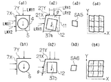
即ち、走査露光時には、移動鏡の反射面が正確にX軸及びY軸に平行であるとすると、ウエハステージ51によってスリット状の露光領域58に対してウエハWが−Y方向に移動するのと同期して、レチクルステージ54によってスリット状の照明領域57に対してレチクルRが−Y方向に移動して、ウエハW上の1つのショット領域にレチクルRのパターン像が転写される。この結果露光されるショット領域は、図10(a3)に拡大して示すショット領域SAaのように正確な矩形であり、ウエハW上に形成されるショット配列は、図10(a4)に示すようにX軸、及びY軸に沿って配列される格子状である。
【0007】
これに対して、ウエハステージ51のヨーイングによって、図10(b1)に示すように移動鏡52X,52Yが角度θだけ時計回りに回転すると、ウエハWの走査方向は、矢印60bで示すように移動鏡52Xの反射面に沿った方向(本来のY軸に対して角度θだけ傾斜した方向)となり、ウエハWの非走査方向へのステッピング方向は、矢印61bで示すように移動鏡52Yの反射面に沿った方向となる。この場合、移動鏡52Yの傾斜によってウエハステージ51の回転が検出され、それに合わせてレチクルステージ54も角度θだけ回転されるため、図10(b2)の矢印59bで示すように、レチクルRも角度θだけ回転した状態で、且つその回転した方向に走査される。従って、走査露光によってウエハW上で露光されるショット領域(レチクルRのパターン像の転写領域)は、図10(b3)のショット領域SAbで示すように、回転はしているが正確な矩形であり、ウエハW上のショット配列(図10(b4)参照)も、回転はしているが配列方向が直交する格子状(以下、「直交格子状」と呼ぶ)である。
【0008】
【発明が解決しようとする課題】
上記の如く従来のステップ・アンド・スキャン方式の投影露光装置では、ウエハステージ及びレチクルステージの座標位置はそれぞれレーザ干渉計によって計測され、レーザ干渉計用の2軸の移動鏡の直交度が良好である場合には、仮にウエハステージがヨーイングによって回転しても露光されるショット領域の形状は矩形であり、得られるショット配列も直交格子状であった。
【0009】
しかしながら、雰囲気気体の温度変化、又は露光光の照射による温度上昇等によって、ステージが熱変形したり、又はレーザ干渉計用の移動鏡自体が熱変形したりすることによって、それらの移動鏡の直交度が悪化したような場合に、露光されるショット領域の形状が矩形でなくなると共に、ショット配列も直交格子状でなくなる恐れがあった。これは主に、従来はステージの走査方向の位置を2軸のレーザ干渉計で計測し、得られた計測値の差分によってステージの回転角を求めていたこと、即ち図10の例では走査方向用の移動鏡52Y,55Yに対してヨーイング計測用のレーザ干渉計からのレーザビームが照射されていたことに依ると考えられる。
【0010】
具体的に、図10(c1)はウエハステージ側の非走査方向用、即ちヨーイング計測が行われない移動鏡52Xが角度θだけ傾斜した状態を示す。この場合、ウエハWの走査方向は矢印60cで示すように、傾斜した移動鏡52Xの反射面に沿った方向であるが、ウエハステージの回転角の変化は検出されないため、図10(c2)に示すように、レチクルR(レチクルステージ54)は−Y方向に走査される。そのため、ウエハW上に形成されるショット領域は、図10(c3)のショット領域SAcで示すように平行四辺形となり、ショット配列(図10(c4)参照)も平行四辺形状となる。
【0011】
また、図10(d1)はウエハステージ側の走査方向用、即ちヨーイング計測が行われている移動鏡52Yが角度θだけ傾斜した状態を示す。この場合、ウエハWの走査方向は−Y方向であるが、ウエハステージの回転角の変化が検出されるため、図10(d2)に矢印59dで示すように、レチクルRは本来のY軸に対して角度θだけ回転した状態で、且つ角度θだけ傾斜した方向に走査される。そのため、ウエハW上に形成されるショット領域は、図10(d3)のショット領域SAdで示すように平行四辺形を90°回転させた形状となり、ショット配列(図10(d4)参照)も同様の形状となる。
【0012】
図10(c4)又は(d4)に示すショット配列の配列誤差は、線形誤差(1次誤差)であるため、その上のレイヤへの露光を行う際には、例えば所謂エンハンスト・グローバル・アライメント(EGA)方式のアライメントを行って統計処理によってショット配列を求め、求められたショット配列に従ってウエハステージのステッピングを行うことによって実質的にその配列誤差が補正できる。しかしながら、ショット領域SAc,SAdで示すようにショット領域の形状が変形した場合、図10(a1)のスリット状の露光領域58のY方向の幅をD、移動鏡の回転角をθ(rad)とすると、ウエハW上に露光される像は走査露光中に非走査方向に略D・θだけ横シフトした像と等価になり、像劣化を起こすという不都合がある。
【0013】
また、所謂ミックス・アンド・マッチ方式で露光を行うため、ショット領域SAc,SAdのような変形したショット領域上にステッパーのような一括露光型の露光装置で重ね合わせ露光を行うものとしても、一括露光型ではそのような変形したショット形状に合わせた補正はできない。そのため、そのような変形したショット領域はディストーション誤差を含むことになり、マッチング精度が悪化するという不都合があった。
【0014】
更に、レーザ干渉計の移動鏡の傾きが変化する場合のみならず、その移動鏡に走査方向に沿った曲がりがある場合にも、露光されるショット領域の形状が歪むという不都合があった。
本発明は斯かる点に鑑み、ステージの位置を計測するための干渉計の移動鏡の角度が変化した場合でも、感光基板上で露光されるショット領域の形状を所望の形状に維持できる走査型露光装置を提供することを第1の目的とする。
【0015】
更に本発明は、その移動鏡に曲がりがある場合でも、感光基板上で露光されるショット領域の形状を所望の形状に維持できる走査型露光装置を提供することを第2の目的とする。
【0016】
【課題を解決するための手段】
本発明による第1の走査型露光装置は、転写用のパターンが形成されたマスク(12)を移動するマスクステージ(9〜11)と、感光性の基板(5)を移動する基板ステージ(1〜4)とを有し、そのマスクを露光用の照明光で照明した状態で、その基板ステージを介して基板(5)を所定方向に走査するのと同期して、そのマスクステージを介してマスク(12)をその所定方向に対応する方向に走査することにより、基板(5)上にマスク(12)のパターンを逐次転写する走査型露光装置において、その基板ステージの走査方向(Y方向)の位置を、この走査方向に直交する非走査方向に沿った2箇所で計測する2軸の基板側干渉計(13Y1,13Y2,7Y)と、その基板ステージのその非走査方向(X方向)の位置をその走査方向に沿った2箇所で計測する2軸の基板側干渉計(13X1,13X2,7X)と、その非走査方向用の2軸の基板側干渉計の計測値に基づいてその基板ステージとそのマスクステージとの相対回転角を補正する回転角補正手段(22D,44R,44L)と、その非走査方向用の2軸の基板側干渉計の計測値の差分と、その走査方向用の2軸の基板側干渉計の計測値の差分との差に基づいて、その基板ステージの移動方向を補正する移動方向補正手段(22A,22B)と、を有するものである。
【0017】
斯かる本発明によれば、例えば図2に示すように、基板(5)を移動するための基板ステージの非走査方向用の移動鏡(7X)に対向して2軸の干渉計本体(13X1,13X2)が配置され、2軸の平均値により座標を定めると共に、これら2軸の計測値の差分よりその基板ステージの非走査方向でのヨーイング量(回転角)が求められ、このヨーイング量に応じてマスク(12)が回転される。この際のマスクステージの回転角は、例えば走査方向、又は非走査方向の何れかに配置した2軸の干渉計の計測値の差分から求めることができる。
【0018】
この結果、例えば図3(c1)〜(c4)に示すように、その基板ステージの非走査方向の移動鏡(7X)の角度が変化した場合、基板(5)及びマスク(12)が同じ角度で傾斜して走査されるため、基板(5)上に露光されるショット領域(SA3)は回転していても矩形のままである。また、例えば図3(d1)〜(d4)に示すように、その基板ステージの走査方向の移動鏡(7Y)の角度が変化した場合、基板(5)及びマスク(12)は共に傾斜することなく走査されるため、基板(5)上に露光されるショット領域(SA4)は矩形のままである。即ち、本発明によって基板(5)及びマスク(12)の走査方向が常に同一となるために、基板(5)上に露光されるショット領域の形状は目標とする形状に維持される。
【0019】
このようにショット領域の形状が目標とする形状となっても、図3(c4)又は(d4)に示すように、ショット配列は直交格子(配列方向が直交する格子)状ではなくなる。このショット配列を更に直交格子状とするために、その非走査方向用の2軸の基板側干渉計(13X1,13X2,7X)の計測値の差分(ヨーイング量)と、その走査方向用の2軸の基板側干渉計(13Y1,13Y2,7Y)の計測値の差分(ヨーイング量)との差に基づいてその基板ステージの移動方向を補正する移動方向補正手段(22A,22B)が設けられている。
【0020】
このとき、本発明によって計測される非走査方向のヨーイング量と、その走査方向のヨーイング量との差を用いて、例えばその基板ステージの非走査方向のステッピング方向を補正すれば、例えば図3(c4)又は(d4)に示されているショット配列が点線で示す直交格子状になる。
次に、マスクステージ側の移動鏡(21X,21Y)が傾斜して直交度が悪化している場合について検討する。この場合にも、従来例のようにそのマスクステージの走査方向用の移動鏡(21Y)の位置を2軸の干渉計で計測し、これら2軸の計測値の差分に基づいてそのマスクステージの回転角を制御すると、露光されるショット領域の形状が矩形でなくなる恐れがある。
【0021】
即ち、図4(a2)及び(b2)、並びに図5(a2)及び(b2)はそれぞれマスクステージの走査方向用の移動鏡(21Y)に対向して2軸の干渉計本体を配置し、非走査方向用の移動鏡(21X)に対向して1軸の干渉計本体を配置した例を示している。また、図4(a1)及び(a2)は、本発明の第1の走査型露光装置と同じく基板ステージの非走査方向の位置を2軸の干渉計で計測する例を示し、図5(a1)及び(a2)は、従来例のように基板ステージの走査方向の位置を2軸の干渉計で計測する例を示している。
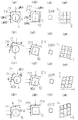
【0022】
これらの場合、図4(a2)、又は図5(a2)に示すように、マスクステージの走査方向の移動鏡(21Y)がマスク(12)に対して角度θだけ傾斜していると、移動鏡(21Y)が基板ステージに対して平行になるように走査されるため、矢印(37a,38a)で示すように、マスク(12)が回転した状態で基板(5)の走査方向に対して傾斜して走査される。従って、露光されるショット領域(SA5,SA7)の形状は平行四辺形を90°回転した形状となる。これに対して、図4(b2)、又は図5(b2)に示すように、マスクステージの非走査方向の移動鏡(21X)がマスク(12)に対して角度θだけ傾斜していると、移動鏡(21Y)が基板ステージに対して平行になるように走査されるために、矢印(37b,38b)で示すように、マスク(12)の走査方向が基板(5)の走査方向に対して傾斜して、露光されるショット領域(SA6,SA8)の形状は平行四辺形となる。
【0023】
そこで、このようなショット領域の変形を避けるため、本発明による第2の走査型露光装置は、転写用のパターンが形成されたマスク(12)を移動するマスクステージ(9〜11)と、感光性の基板(5)を移動する基板ステージ(1〜4)とを有し、マスク(12)を露光用の照明光で照明した状態で、その基板ステージを介して基板(5)を所定方向(Y方向)に走査するのと同期して、そのマスクステージを介してマスク(12)をその所定方向に対応する方向(Y方向)に走査することにより、基板(5)上にマスク(12)のパターンを逐次転写する走査型露光装置において、その基板ステージの走査方向に直交する非走査方向(X方向)の位置をその走査方向に沿った2箇所で計測する2軸の基板側干渉計(13X1,13X2,7X)と、そのマスクステージの走査方向に直交する非走査方向の位置をそのマスクステージの走査方向に沿った2箇所で計測する2軸のマスク側干渉計(14X1,14X2,21X)と、その2軸の基板側干渉計の計測値、及びその2軸のマスク側干渉計の計測値に基づいてその基板ステージとそのマスクステージとの相対回転角を補正する回転角補正手段(22D,44R,44L)と、を有するものである。
【0024】
斯かる本発明によれば、例えば図7に示すように、基板ステージの非走査方向の移動鏡(7X)の位置が2軸の干渉計で計測され、マスクステージの非走査方向の移動鏡(21X)の位置も2軸の干渉計で計測され、移動鏡(7X)の2箇所の計測値の差分よりその基板ステージのヨーイング量が求められ、移動鏡(21X)の2箇所の計測値の差分よりそのマスクステージの回転角が求められる。従って、図7(a2)又は(b2)に示すように、マスクステージ側の走査方向の移動鏡(21Y)、又は非走査方向の移動鏡(21X)の何れかがマスク(12)に対して傾斜しても、マスク(12)の走査方向は基板(5)の走査方向に平行になり、露光されるショット領域(SA13,SA14)の形状は、回転(ショットローテーション)は生じても矩形となる。
【0025】
次に、本発明の実施の形態に記載された走査型露光装置は、転写用のパターンが形成されたマスク(12)を移動するマスクステージ(9〜11)と、感光性の基板(5)を移動する基板ステージ(1〜4)とを有し、マスク(12)を露光用の照明光で照明した状態で、その基板ステージを介して基板(5)を所定方向(Y方向)に走査するのと同期して、そのマスクステージを介してマスク(12)をその所定方向に対応する方向(Y方向)に走査することにより、基板(5)上にマスク(12)のパターンを逐次転写する走査型露光装置において、その基板ステージ、及びそのマスクステージの一方のステージ(9〜11)の走査方向の位置をこの走査方向に直交する非走査方向に沿った2箇所で計測する第1の2軸の干渉計(14Y1,14Y2,21Y)と、その一方のステージのその非走査方向の位置をこのステージの走査方向に沿った2箇所で計測する第2の2軸の干渉計(14X1,14X2,21X)と、この第1の2軸の干渉計の計測値の差分に基づいてその一方のステージの回転角を検出し、この検出結果、及びその第2の2軸の干渉計の計測値の差分に基づいてその第2の2軸の干渉計用の移動鏡(21X)の曲がり量を算出する移動鏡曲がり量算出手段(22A)と、を備えたものである。
【0026】
斯かる本発明によれば、例えばそのマスクステージの走査方向の位置計測用に2軸の干渉計(14Y1,14Y2,21Y)を配置し、非走査方向の位置計測用に2軸の干渉計(14X1,14X2,21X)を配置した場合、例えば図9に示すように、非走査方向の干渉計の移動鏡(21X)が曲がっていると、マスク(12)は曲がりながら走査されるため、露光されるショット領域が歪む可能性がある。そこで、マスクステージを走査方向に移動させたときに、走査方向の2軸の干渉計の計測値の差分が一定になるようにしてそのマスクステージのヨーイングが発生しないようにする。この状態で、非走査方向用の2軸の干渉計の計測値の差分をモニタすると、非走査方向の移動鏡(21X)の曲がり形状が計測できる。実際の走査露光時には、そのように計測された移動鏡(21X)の曲がり分だけ、その2軸の干渉計の計測値を補正することによって、そのマスクステージが走査方向に直線的に移動して、より矩形に近いショット領域が露光される。
【0027】
また、上述の本発明の各走査型露光装置においては、その基板ステージ及びそのマスクステージの一方のステージの走査方向に直交する非走査方向の位置を計測する2軸の干渉計の計測値の差分をモニタし、このようにモニタされる差分が所定の閾値を超えた際に、マスク(12)とその基板ステージとの位置関係を計測する計測手段(6,19,20)を更に備えることが望ましい。そのように2軸の干渉計の計測値の差分が所定の閾値を超えるのは、熱変形等によって干渉計用の移動鏡の傾斜角が大きく変化したためと予想される。このときにマスク(12)とその基板ステージとの位置関係を再計測することによって、マスク(12)と基板(5)との位置関係を補正できるため、露光されるショット領域の形状誤差が減少する。また、このような場合、移動鏡の曲がり量も変化している可能性があるので、移動鏡の曲がり量をも再計測するようにしてもよい。
次に、本発明による第3の走査型露光装置は、転写用のパターンが形成されたマスク(12)を保持して移動するマスクステージ(9〜11)と、感光性の基板(5)を保持して移動する基板ステージ(1〜4)とを有し、そのマスクを露光用の照明光で照明した状態で、そのマスクステージとその基板ステージとをそれぞれ走査方向に沿って互いに反対方向に互いに異なる速度で同期して走査することにより、その基板上にそのマスクのパターンを逐次転写する走査型露光装置において、そのマスクステージの、その走査方向に直交する非走査方向の位置を、その走査方向に沿って離れた複数箇所で計測する複数軸のマスク側干渉計(14X1,14X2,21X)を有し、そのマスク側干渉計は、そのマスクステージがその走査方向に移動している最中に、その非走査方向におけるそのマスクステージの位置を、その複数箇所で同時に測定すると共に、各計測軸毎にその測定値を出力するものである。
本発明によれば、その複数軸のマスク側干渉計の測定値を用いることによって、そのマスクステージの走査中にそのマスクステージの回転角を測定できる。従って、そのマスクステージの回転角を例えばその基板ステージの走査方向に応じて制御することによって、その基板上に露光されるショット領域の形状を目標とする形状に維持できる。
本発明において、その複数軸のマスク側干渉計の計測値に基づいて、その基板ステージとそのマスクステージとの相対回転角を補正する回転角補正手段(22D,44R,44L)を更に有してもよい。その回転角補正手段を用いて、例えばそのマスクとその基板との走査方向を同一にすることによって、その基板上に露光されるショット領域の形状を目標とする形状に維持できる。
また、その基板ステージの、その走査方向に直交する非走査方向の位置を、その走査方向に沿って離れた複数箇所で計測する複数軸の基板側干渉計(13X1,13X2,7X)を更に有し、その基板側干渉計は、その基板ステージがその走査方向に移動している最中に、その非走査方向におけるその基板ステージの位置を、その複数箇所で同時に測定すると共に、各計測軸毎にその測定値を出力してもよい。
また、その複数軸の基板側干渉計の計測値、及びその複数軸のマスク側干渉計の計測値に基づいてその基板ステージとそのマスクステージとの相対回転角を補正する回転角補正手段(22D,44R,44L)を更に有してもよい。
【0028】
【発明の実施の形態】
以下、本発明による走査型露光装置の実施の形態の一例につき図面を参照して説明する。本例は、ステップ・アンド・スキャン方式の投影露光装置に本発明を適用したものである。
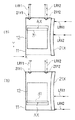
図1は本例の投影露光装置を示し、この図1において、図示省略された照明光学系からの露光光ELによる矩形の照明領域(以下、「スリット状の照明領域」という)によりレチクル12上のパターンが照明され、そのパターンの像が投影光学系8を介してフォトレジストが塗布されたウエハ5上に投影される。この状態で、露光光ELのスリット状の照明領域に対して、レチクル12が図1の紙面に対して前方向(又は後方向)に一定速度Vで走査されるのに同期して、ウエハ5は図1の紙面に対して後方向(又は前方向)に一定速度V/M(1/Mは投影光学系8の投影倍率)で走査される。投影倍率(1/M)は、例えば1/4,1/5等である。以下、投影光学系8の光軸AXに平行にZ軸を取り、Z軸に垂直な平面内でレチクル12及びウエハ5の設計上の走査方向(即ち、図1の紙面に垂直な方向)にY軸を、この走査方向に直交する非走査方向(即ち、図1の紙面に沿った方向)にX軸を取って説明する。但し、後述のようにステージ系の座標計測用の干渉計の移動鏡の傾斜等によって、実際の走査方向はY軸に平行な方向(Y方向)から外れることがある。
【0029】
次に、本例のレチクル12及びウエハ5のステージ系について説明する。先ず、レチクル支持台9上にY方向に駆動自在にレチクルY軸駆動ステージ10が載置され、このレチクルY軸駆動ステージ10上にレチクル微小駆動ステージ11が載置され、レチクル微小駆動ステージ11上にレチクル12が真空チャック等により保持されている。レチクル微小駆動ステージ11は、X方向、Y方向及び回転方向(θ方向)にそれぞれ微小量だけ且つ高精度にレチクル12の位置制御を行う。レチクル支持台9、レチクルY軸駆動ステージ10、及びレチクル微小駆動ステージ11よりレチクルステージが構成されている。レチクル微小駆動ステージ11上には移動鏡21が配置され、レチクル支持台9上に配置された干渉計本体14によって、常時レチクル微小駆動ステージ11のX方向、Y方向及びθ方向の位置がモニタされている。即ち、干渉計本体14は実際には、図2(a)に示す4軸の干渉計本体14X1,14X2,14Y1,14Y2を総称している。干渉計本体14により得られた位置情報が、装置全体の動作を統轄制御する主制御系22Aに供給されている。主制御系22Aは、レチクル駆動装置22Dを介してレチクルY軸駆動ステージ10及びレチクル微小駆動ステージ11の動作を制御する。
【0030】
一方、ウエハ支持台1上には、Y方向に駆動自在にウエハY軸駆動ステージ2が載置され、その上にX方向に駆動自在にウエハX軸駆動ステージ3が載置され、その上にZθ軸駆動ステージ4が設けられ、このZθ駆動ステージ4上にウエハ5が真空吸着によって保持されている。Zθ軸駆動ステージ4は、ウエハ5のZ方向の位置、傾斜角、及び微小回転角の制御を行う。ウエハ支持台1、ウエハY軸駆動ステージ2、ウエハX軸駆動ステージ3、及びZθ軸駆動ステージ4よりウエハステージが構成されている。Zθ軸駆動ステージ4上にも移動鏡7が固定され、外部に配置された干渉計本体13により、Zθ軸駆動ステージ4のX方向、Y軸方向及びθ方向の位置がモニタされ、干渉計本体13により得られた位置情報も主制御系22Aに供給されている。即ち、干渉計本体13も実際には、図2(b)に示す4軸の干渉計本体13X1,13X2,13Y1,13Y2を総称している。主制御系22Aは、ウエハ駆動装置22Bを介してウエハY軸駆動ステージ2、ウエハX軸駆動ステージ3、及びZθ軸駆動ステージ4の位置決め動作を制御する。
【0031】
また、後述するが、ウエハステージ側の干渉計本体13によって計測される座標により規定されるウエハ座標系と、レチクルステージ側の干渉計本体14によって計測される座標により規定されるレチクル座標系との対応をとるために、Zθ軸駆動ステージ4上のウエハ5の近傍に所定の基準マークが形成された基準マーク板6が固定されている。その基準マーク中にはZθ軸駆動ステージ4の内部に導かれた照明光により底面側から照明されている基準マーク、即ち発光性の基準マークもある。
【0032】
本例のレチクル12の上方には、基準マーク板6上の基準マークとレチクル12上のアライメントマークとを同時に観察するためのレチクルアライメント顕微鏡19及び20が配置されている。この場合、レチクル12からの検出光をそれぞれアライメント顕微鏡19及び20に導くための偏向ミラー15及び16が移動自在に配置され、露光シーケンスが開始されると、主制御系22Aからの指令のもとで、ミラー駆動装置17及び18によりそれぞれ偏向ミラー15及び16は退避される。更に、投影光学系8のY方向の側面部に、ウエハ5上のアライメントマーク(ウエハマーク)の位置を検出するためのオフ・アクシス方式のアライメントセンサ34が配置されている。また、主制御系22Aには、オペレータからのコマンドを入力したり、計測データを表示したりするためのコンソール22Cが接続されている。
【0033】
次に、図2を参照して本例のステージ系用の干渉計(干渉式測長器)の構成につき説明する。
図2(a)は、図1のレチクル微小駆動ステージ11を示す平面図、図2(b)は、図1のウエハステージ側のZθ軸駆動ステージ4を示す平面図であり、図2(a)において、レチクル微動ステージ11上にはレチクル12が真空吸着等によって保持され、レチクル12上のX方向に細長いスリット状の照明領域31に露光光が照射されている。
【0034】
レチクル12(レチクル微小駆動ステージ11)はY方向に走査されるため、レチクル微小駆動ステージ11の+X方向の端部に、走査方向(Y方向)に沿って延びた平行平板ガラスよりなる移動鏡21Xが設置され、干渉計本体14X1及び14X2より移動鏡21Xの反射面に、Y方向に間隔L1で平行に計測用のレーザビーム(計測用ビーム)LRX1及びLRX2が照射されている。干渉計本体14X1,14X2はそれぞれ参照鏡と、移動鏡21X及びその参照鏡からのレーザビームの干渉光を受光するレシーバと、このレシーバからの光電変換信号を処理する信号処理部とを備え、そのレシーバからの光電変換信号を処理することによって移動鏡21Xの反射面のX座標が検出できるように構成されている。移動鏡21Xはレチクル12の加速、露光、減速時に両計測用ビームLRX1,LRX2が移動鏡21Xから外れることが無いように十分長く形成されている。更に、計測用ビームLRX1,LRX2は、スリット状の照明領域31の中心(投影光学系8の光軸AX)に対してY方向に振り分けになるように配置されており、干渉計本体14X1及び14X2の計測値をそれぞれXR1及びXR2とすると、これらの計測値の平均値としてレチクル12の非走査方向の位置(X座標)XRが検出され、それらの計測値の差分を間隔L1で除算することによって、レチクル12の非走査方向から見た回転角θRXが検出される。即ち、次式が成立している。
【0035】
XR=(XR1+XR2)/2 (1)
θRX=(XR1−XR2)/L1 (2)
また、レチクル微小駆動ステージ11の+Y方向の端部には、X方向に間隔L2で移動鏡としてのコーナキューブ21Y1,21Y2が固定されており、コーナキューブ21Y1,21Y2に対してそれぞれ干渉計本体14Y1,14Y2より、走査方向に沿って平行に計測用ビームLRY1,LRY2が照射されている。また、コーナキューブ21Y1,21Y2で反射された計測用ビームLRY1,LRY2をそれぞれ反射して干渉計本体14Y1,14Y2側に戻す固定平面鏡14M1及び14M2が配置され、干渉計本体14Y1,14Y2はそれぞれダブルパス干渉方式でコーナキューブ21Y1,21Y2のY座標を検出する。なお、レチクル12はX方向の移動範囲は狭いと共に、コーナキューブ21Y1,21Y2の入射面に計測用ビームLRY1,LRY2が収まっている範囲では正確に位置検出を行うことができるため、走査方向の移動鏡としてはコーナキューブ21Y1,21Y2を使用できる。
【0036】
計測用ビームLRY1,LRY2も、照明領域31の中心(光軸AX)に関してX方向に中心対称に振り分けされており、干渉計本体14Y1及び14Y2の計測値YR1,YR2の平均値によってレチクル12の走査方向の位置(Y座標)YRが検出される。また、それらの計測値の差分を間隔L2で除算することによってレチクル12の走査方向から見た回転角θRYが検出される。また、走査方向から見た回転角θRYと非走査方向から見た回転角θRXとの差分が、移動鏡21Xとコーナキューブ21Y1,21Y2との直交度誤差ΔωRとなる。即ち、次式が成立している。
【0037】
YR=(YR1+YR2)/2 (3)
θRY=(YR1−YR2)/L2 (4)
ΔωR=(YR1−YR2)/L2−(XR1−XR2)/L1 (5)
本例では通常は、(2)式の非走査方向から見た回転角θRXに基づいてレチクル12の回転角(ヨーイング量)の補正を行う。そのため、レチクル微小駆動ステージ11の−Y方向の端面に2個のアクチュエータ44R及び44Lが設置され、アクチュエータ44R及び44Lで互いに独立に図1のレチクルY軸駆動ステージ10に対してレチクル微小駆動ステージ11を変位させることによって、レチクル微小駆動ステージ11(レチクル12)の回転角が制御できるように構成されている。アクチュエータ44R,44Lの動作は図1のレチクル駆動装置22Dによって制御されている。但し、後述のように、移動鏡21Xの曲がり量をモニタする際には、(4)式の走査方向から見た回転角θRYに基づいてレチクル12の回転角を制御する。
【0038】
図2(a)において、移動鏡21X及び干渉計本体14X1,14X2より非走査方向用の2軸のレーザ干渉計が構成され、コーナキューブ21Y1,21Y2、固定平面鏡14M1,14M2、及び干渉計本体14Y1,14Y2より走査方向用の2軸のレーザ干渉計が構成されている。そして、干渉計本体14X1,14X2によって計測されるX座標XR、及び干渉計本体14Y1,14Y2によって計測されるY座標YRよりなる座標系をレチクルステージの座標系(XR,YR)と呼ぶ。この座標系は、X軸及びY軸よりなる設計上の理想的な直交座標系とは或る程度異なっている場合があるが、レチクル12はそのレチクルステージの座標系(XR,YR)に基づいて駆動される。
【0039】
次に、図2(b)において、Zθ軸駆動ステージ4上にはウエハ5が真空吸着等によって保持され、ウエハ5の近傍に基準マーク板6が固定されている。基準マーク板6上には、走査方向に沿って発光性の2列の基準マーク46A〜46Fが形成され、レチクル12上にも対応して2列のアライメントマーク45A〜45Fが形成されている。両マークを図1のアライメント顕微鏡19,20で検出することによってレチクルステージの座標系とウエハステージの座標系との対応が取られる。この詳細は例えば特開平7−176468号公報にも開示されている。
【0040】
また、ウエハ5上でレチクル上の照明領域31と共役なスリット状の露光領域32にレチクル12の一部のパターンの像が投影され、露光領域32に対してウエハ5をY方向に走査することによって、ウエハ5上の1つのショット領域SAにレチクル12のパターンが転写される。Zθ軸駆動ステージ4の−X方向の端部に、走査方向(Y方向)に沿って延びた平行平板ガラスよりなる移動鏡7Xが設置され、Zθ軸駆動ステージ4の−Y方向の端部に移動鏡7Xに直交するように非走査方向に沿って延びた平行平板ガラスよりなる移動鏡7Yが固定されている。干渉計本体13X1及び13X2より移動鏡7Xの反射面に、Y方向に間隔L3で平行に計測用ビームLWX1及びLWX2が照射され、干渉計本体13Y1及び13Y2より移動鏡7Yの反射面に、X方向に間隔L4で平行に計測用ビームLWY1及びLWY2が照射されている。
【0041】
移動鏡7X,7Yはウエハ5の走査露光、又はステッピング時に対応する計測用ビームが外れることが無いように十分長く形成されている。更に、計測用ビームLWX1,LWX2は、スリット状の露光領域32の中心(光軸AX)に対してY方向に振り分けになるように配置されており、干渉計本体13X1及び13X2の計測値XW1,XW2の平均値によってウエハ5の非走査方向の位置(X座標)XWが検出され、干渉計本体13Y1及び13Y2の計測値YW1,YW2の平均値によってウエハ5の走査方向の位置(Y座標)YWが検出される。また、計測値XW1,XW2の差分を間隔L3で除算することによって、ウエハ5のヨーイング量(回転角)θWXが検出され、計測値YW1,YW2の差分を間隔L4で除算した回転角θWYと、そのヨーイング角θWXとの差分によって移動鏡7X,7Yの直交度誤差ΔωWが検出される。即ち、次式が成立している。
【0042】
XW=(XW1+XW2)/2 (6)
YW=(YW1+YW2)/2 (7)
θWX=(XW1−XW2)/L3 (8)
ΔωW=(YW1−YW2)/L4−(XW1−XW2)/L3 (9)
図2(b)において、移動鏡7X及び干渉計本体13X1,13X2より非走査方向用の2軸のレーザ干渉計が構成され、移動鏡7Y及び干渉計本体13Y1,13Y2より走査方向用の2軸のレーザ干渉計が構成されている。このように干渉計本体13X1,13X2によって計測されるX座標XW、及び干渉計本体13Y1,13Y2によって計測されるY座標YWよりなる座標系をウエハステージの座標系(XW,YW)と呼ぶ。この座標系も、X軸及びY軸よりなる設計上の理想的な直交座標系とは或る程度異なっている場合があるが、ウエハ5の走査、及びステッピングはそのウエハステージの座標系(XW,YW)に沿って行われる。例えば(9)式の直交度誤差ΔωWの補正を行わない場合、Zθ軸駆動ステージ4(ウエハ5)のステッピング方向は、走査方向では、移動鏡7Xの反射面に沿った方向(X座標XWが変化しない方向)となり、非走査方向では移動鏡7Yの反射面に沿った方向(Y座標YWが変化しない方向)となる。
【0043】
次に、本例の投影露光装置でアライメント、走査露光、及びステッピングを行う際の基本的な動作につき説明する。先ず、図2(b)の基準マーク板6を用いてレチクルアライメントを行う。即ち、図1のウエハY軸駆動ステージ2及びウエハX軸駆動ステージ3を駆動することによって、基準マーク板6の基準マーク46A,46Bを投影光学系8の露光領域32内に移動して静止させ、レチクルY軸駆動ステージ10を駆動して図2(a)のレチクル12上のアライメントマーク45A,45Bを照明領域31内に移動する。そして、図1のアライメント顕微鏡19及び20によって、基準マーク46A,46Bと対応するアライメントマーク45A,45Bとの位置ずれ量を検出し、レチクルY軸駆動ステージ10及びレチクル微小駆動ステージ11を駆動して、基準マーク46A及び46Bの像に対してアライメントマーク45A及び45Bの位置ずれ量が対称になるように合わせ込む。これによって、レチクル12の位置、及び回転角が基準マーク板6に対して合わせ込まれる。また、この状態で例えば、レチクルステージ側の4軸の干渉計本体14の計測値、及びウエハステージ側の4軸の干渉計本体13の計測値をリセットすることによって、(1)式及び(3)式より定まるレチクルステージの座標系(XR,YR)と、(6)式及び(7)式より定まるウエハステージの座標系(XW,YW)との原点のオフセットが補正される。
【0044】
また、予め走査露光時のウエハステージ側のZθ軸駆動ステージ4の走査方向を基準マーク板6の基準マークの配列方向に平行にしておく。このためには、一例として機械的に基準マーク46A,46C,46Eの配列方向を移動鏡7Xの反射面(走り面)に平行にしておけばよい。但し、機械的な調整誤差が残存する際には、ウエハステージのY座標YWが所定ステップ変化する毎に、そのX座標XWが対応する量だけ変化するようにして、ソフトウェア的にZθ軸駆動ステージ4の走査方向を補正してもよい。以下ではこのように補正された走査方向をY軸とする座標系をウエハステージの座標系(XW,YW)と呼ぶ。
【0045】
次に、露光光を照射することなく、走査露光時と同様にウエハステージ側のステージとレチクルステージ側のステージとを同期走査すると共に、基準マーク板6上の基準マーク46C〜46Fと対応するレチクル12上のアライメントマーク45C〜45Fとの相対的な位置ずれ量をアライメント顕微鏡19,20によって順次検出する。これらの相対的な位置ずれ量の平均値より、レチクル12の走査方向とウエハ5の走査方向との傾き角、即ちレチクルステージの座標系(XR,YR)と、ウエハステージの座標系(XW,YW)との走査方向の軸の回転角を求める。その後、レチクル12を走査する際には、レチクルY軸駆動ステージ10及びレチクル微小駆動ステージ11を介してY座標YRが所定間隔変化する間にX座標XRを対応する量だけ横ずれさせることによって、ソフトウェア的にレチクル12の走査方向を基準マーク板6の基準マークの配列方向に合わせ込む。以下ではこのように補正された走査方向をY軸とする座標系をレチクルステージの座標系(XR,YR)と呼ぶ。この結果、ウエハステージの座標系(XW,YW)及びレチクルステージの座標系(XR,YR)は、基準マーク板6を基準として走査方向の軸が互いに平行になり、走査露光時にレチクル12及びウエハ5は平行に走査される。
【0046】
この場合、各ステージの移動は各ステージのガイド面基準であり、投影露光装置の組立調整時に、例えばレチクルY軸駆動ステージ10のガイド面とウエハY軸駆動ステージ2のガイド面との平行度を数100μrad程度以下に機械的に合わせておく。更に、それらのガイド面に対して移動鏡及び基準マーク板6を合わせて固定することで、走査露光時に各ステージを非走査方向へも駆動することによるソフトウェア的な補正量を小さくし、制御精度を向上させている。このように調整されたレチクル微小駆動ステージ11に対し、実際にレチクル12を載置した場合、レチクル12が外形基準等で設置されると、各移動鏡及び基準マーク板6に対しレチクル12のアライメントマーク45A〜45Fのみが大きく回転している可能性がある。これは、レチクルの外形と転写用パターンとの間の位置ずれ量は大きいときには0.5mm程度あるからである。
【0047】
図2(a)のレチクル12の外形と転写用パターンとの位置ずれ量が大きいと、レチクル12のアライメントマーク45A〜45Fと基準マーク板6の基準マーク46A〜46Fとの位置ずれ量を計測した場合、相対的にレチクル12又は基準マーク板6が大きく回転しているか、大きなオフセットを持っているように計測される。しかし、基準マーク板6は移動鏡7X,7Yの走りに合わせて固定されているので、レチクル微小駆動ステージ11を回転又はシフトさせることで補正が行われる。ここで、レチクル微小駆動ステージ11を回転させた場合、移動鏡21Xも同様に回転するので、レチクル12の走り方向に対し移動鏡21Xが傾くこととなるが、レチクル12上のアライメントマーク45A〜45Fは基準マーク板6上の基準マーク46A〜46Fに平行になっており、走査露光時にはレチクル12の走り方向とウエハ5の走り方向とが平行となるように制御される。
【0048】
次に、ウエハ5上の各ショット領域のウエハステージの座標系(XW,YW)上での配列を求めるためのウエハアライメントが行われる。一例として、図1のアライメントセンサ34を用いてウエハ5上から選択された所定個数のショット領域(サンプルショット)のウエハマークの座標を計測し、この計測結果を統計処理するEGA(エンハンスト・グローバル・アライメント)方式でウエハ5上の全部のショット領域の配列座標が算出される。また、予め所謂ベースラインチェックによって、基準マーク板6を用いて、アライメントセンサ34の検出中心と、投影光学系8の露光領域32内の基準点との間隔(ベースライン量)が求められて主制御系22A内に記憶されている。そこで、ウエハ5上の各ショット領域の配列座標、アライメントセンサ34のベースライン量、及びウエハステージの座標系(XW,YW)とレチクルステージの座標系(XR,YR)との関係に基づいて、ウエハ5上の露光対象のショット領域が走査開始位置に位置決めされると共に、レチクル12も対応する位置に位置決めされる。
【0049】
その後、先のレチクルアライメント時に定められたウエハステージの座標系(XW,YW)及びレチクルステージの座標系(XR,YR)に従って走査露光動作が行われるが、その座標系は各移動鏡7X,7Y,21X及びコーナキューブ21Y1,21Y2の反射面を基準としてソフトウェア的に補正されたものであり、これらの移動鏡等の位置がレチクル12やウエハ5に対して相対的にずれた場合、ショット領域の形状やショット配列に影響を及ぼすこととなる。本例ではこのようなときでも正確な矩形のショット領域、及び直交格子状のショット配列が形成されるように、以下の方法により走査露光及びステッピングを行っている。
【0050】
即ち、ウエハアライメントによって、露光対象のショット領域とレチクルとが位置合わせされたときのレチクルステージの座標系(XR,YR)の座標を(XR0,YR0)、ウエハステージの座標系(XW,YW)の座標を(XW0,YW0)とすると、投影光学系8の投影倍率は1/Mであるため、それ以後のレチクル微小駆動ステージ11(レチクル12)とZθ軸駆動ステージ4(ウエハ5)との走査方向、及び非走査方向の同期誤差ΔX,ΔYは次のように表すことができる。但し、これらの同期誤差はレチクル12上に換算した誤差である。また、図1の投影光学系8は反転投影系であるが、図2に示すように、レチクルステージ側の干渉計とウエハステージ側の干渉計とは計測方向が反転しているため、同期誤差は単に移動量の倍率補正値の差分を取るだけで求められる。
【0051】
ΔX=(XW−XW0)・M−(XR−XR0) (10)
ΔY=(YW−YW0)・M−(YR−YR0) (11)
また、本例では(8)式で表されるZθ軸駆動ステージ4の非走査方向から見た回転角θWXと、(2)式で表されるレチクル微小駆動ステージ11の非走査方向から見た回転角θRXとの差分を次のように回転方向の同期誤差Δθとする。
【0052】

【0053】
その後、次のショット領域への露光を行うためにウエハ5のステッピングを行う際には、ウエハステージ側の移動鏡7X,7Yの直交度が悪化したときでも、ショット配列が直交格子(配列方向が直交する格子)状を維持するように、Zθ軸駆動ステージ4の非走査方向のステッピング方向を(9)式の直交度誤差ΔωW分だけ補正する。
【0054】
更に、(9)式の直交度誤差ΔωW、又は(5)式の直交度誤差ΔωRが所定の許容値を超えて大きく変化する場合は、その他のオフ・アクシス方式のアライメントセンサ34のベースライン量の精度やその機械的な安定性に問題が発生している可能性がある。そこで、直交度誤差ΔωW、又はΔωRが所定の許容値を超えて大きく変化している場合は、ウエハの交換時等に再度上記のレチクルアライメントやベースライン量の計測を行うようにする。これによって、レチクルのパターンとウエハの各ショット領域との重ね合わせ精度を向上できる。
【0055】
次に、本例の投影露光装置で走査露光を行うことによって得られるショット領域の形状、及びショット配列の具体例につき説明する。
先ず、図3を参照して、図2に示すレチクルステージ側の移動鏡の直交度が良好で、且つウエハステージ側の移動鏡7X,7Yの傾きが変化した場合につき説明する。
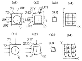
【0056】
図3(a1)〜(d1)は図2(b)のウエハ5が載置されるZθ軸駆動ステージ4上の移動鏡7X,7Yを簡略化して示し、図3(a2)〜(d2)は図2(a)のレチクル12が載置されるレチクル微小駆動ステージ11上の移動鏡21X、及びコーナキューブ21Y1,21Y2を簡略化して示し、コーナキューブ21Y1,21Y2をまとめて1つの移動鏡21Yとしている。また、分かり易いように、図1の投影光学系8によって正立像がウエハ上に投影されるものと仮定して、図2に対してウエハステージ側の移動鏡7Yを+Y方向側に固定し、レチクルステージ側の移動鏡21Xを−X方向側に固定している。これによって、ウエハ5及びレチクル12の走査方向は同じ方向(−Y方向、又は+Y方向)となっている。これは以下の図4〜図7においても同様である。
【0057】
また、図3では、レチクル12のパターン領域の輪郭は移動鏡21X、又は21Yの反射面に平行であると仮定している。更に、ウエハステージ側の走査方向用の移動鏡7Yに対して1本の計測用ビームLWY1が照射され、レチクルステージ側の非走査方向用の移動鏡21Xに対して1本の計測用ビームLRX1が照射されているものとしている。これは、走査露光中には、ウエハステージ側では走査方向用の移動鏡7Yの回転角はモニタすることなく、レチクル側では非走査方向用の移動鏡21Xの回転角はモニタしないことを意味している。但し、上記のようにレチクル側では通常は非走査方向用の移動鏡21Xの回転角がモニタされているが、後述のようにレチクルステージ側の移動鏡21X,21Yの直交度が良好であるときには、どちらの移動鏡の回転角をモニタしても同じ結果が得られるため、図3では走査方向用の移動鏡21Yの回転角をモニタしている。この場合、(12)式の同期誤差Δθの代わりに、(8)式のウエハの回転角θWXと(4)式のレチクルの回転角θRYとの差分である次式の同期誤差Δθ’が0になるようにレチクル微小駆動ステージ11の回転角が補正される。
【0058】
Δθ’=θWX−θRY (13)
そして、図3(a1)に示すように、走査露光中にウエハステージ側のZθ軸駆動ステージ4の移動鏡7X,7Yの直交度が良好で、且つ移動鏡7Xが理想的な直交座標系のY軸に平行(移動鏡7XはX軸に平行)であるときには、走査露光中に上記の(10)式の同期誤差ΔX、(11)式の同期誤差ΔY、及び(13)式の同期誤差Δθ’がそれぞれ0になるように走査が行われるため、図3(a2)に示すように、レチクル微小駆動ステージ11(レチクル12)は照明領域31に対してY軸に平行に走査される。また、ウエハ5上のショット領域SA1も露光領域32に対してY軸に平行に走査されるため、そのショット領域SA1の形状は、図3(a3)に拡大して示すように正確な矩形である。更に、1つのショット領域から次のショット領域に移動する際の、ウエハステージ側のZθ軸駆動ステージ4のステッピング方向は、X軸及びY軸に平行であるため、ウエハ5上に形成されるショット配列は、図3(a4)に示すように直交格子状である。
【0059】
次に、図3(b1)に示すように、走査露光中にウエハステージ側の移動鏡7X,7Yの直交度が良好で、且つZθ軸駆動ステージ4が角度θだけ時計方向に回転したときには、ウエハ5は矢印34bに示すようにY軸に対して角度θだけ傾斜して走査される。また、レチクル微小駆動ステージ11(レチクル12)も角度θだけ時計方向に回転して走査されるため、ウエハ5上のショット領域SA2の形状は、図3(b3)に示すように回転はしているが正確な矩形である。更に、ウエハステージ側のZθ軸駆動ステージ4のステッピング方向は、走査方向では矢印34bで示す方向であり、非走査方向では矢印35bで示すように移動鏡7Yの反射面に沿った方向であるため、ウエハ5上に形成されるショット配列は、図3(b4)に示すように回転はしているが直交格子状である。
【0060】
これに対して、図3(c1)に示すように、図3(a1)と比べてウエハステージ側の非走査方向の移動鏡7Xの角度がθだけ変化した場合、ウエハ5は矢印34cで示すようにY軸に対して角度θだけ傾斜して走査され、レチクル12も図3(c2)に矢印33cで示すようにY軸に対して角度θ傾斜して走査される。その結果、図3(c3)に示すように、ウエハ5上で露光されるショット領域SA3の形状は、矩形のままである。但し、この際にウエハ側で単に移動鏡7X,7Yに沿ってステッピングを行うと、移動鏡7X,7Yの直交度誤差が生じているために、ウエハ5上のショット配列は図3(c4)に示すように平行四辺形状となり、直交格子ではなくなる。これに対して本例では、図3(c1)に点線で示すように、移動鏡7Yには更に1軸の計測用ビームLWY2が照射されており、Zθ軸駆動ステージ4(ウエハ5)の非走査方向のステッピング方向は(9)式の直交度誤差ΔωW分だけ補正される。即ち、ウエハ5の非走査方向のステッピング方向は、図3(c1)の矢印47cで示すように、移動鏡7Yに対して角度θだけ時計回りに回転している。従って、ウエハ5上のショット配列は、図3(c4)に点線の格子48cに示すように、回転はしているが直交格子状となる。
【0061】
一方、図3(d1)に示すように、図3(a1)と比べてウエハステージ側の走査方向の移動鏡7Yの角度がθだけ反時計回りに変化した場合、ウエハ5は−Y方向に走査される。また、移動鏡7Xの傾斜角はレチクル12の回転角の補正には使用されないため、レチクル12も図3(d2)に示すように−Y方向に走査され、図3(d3)に示すように、ウエハ5上で露光されるショット領域SA4の形状は、矩形のままである。この際にも、ウエハ側で単に移動鏡7X,7Yに沿ってステッピングを行うと、ウエハ5上のショット配列は図3(d4)に示すように平行四辺形を90°回転したような配列となる。実際には本例では、ウエハ5の非走査方向のステッピング方向は(9)式の直交度誤差ΔωW分だけ補正されるため、ウエハ5の非走査方向のステッピング方向は、図3(d1)の矢印47dで示すように、移動鏡7Yに対して角度θだけ時計回りに回転している。従って、ウエハ5上のショット配列は、図3(d4)に点線の格子48dで示すように、正確な直交格子状となる。
【0062】
なお、図3ではレチクル12の回転角を走査方向用の移動鏡21Yの回転角に基づいて補正する場合を示したが、本例では通常はレチクル12の回転角は非走査方向用の移動鏡21Xの回転角に基づいて制御されている。
図6は、そのようにレチクル12の回転角を非走査方向用の移動鏡21Xの回転角に基づいて補正する場合を示し、この図6において、移動鏡21Xに2本の計測用ビームLRX1,LRX2が照射され、移動鏡21Yには1本の計測用ビームLRY1のみが照射されている点以外は図3と同一である。図6においても、ウエハステージ側の非走査方向の移動鏡7Xの傾斜角に応じてレチクル12の回転角が補正されるため、ウエハステージ側の移動鏡7X,7Yの直交度が良好であるときには(図6(a1),(b1))、レチクル12の走査方向はウエハ5の走査方向に平行となり(図6(a2),(b2))、露光されるショット領域SA9,SA10の形状は矩形であり(図6(a3),(b3))、形成されるショット配列も直交格子状である(図6(a4),(b4))。
【0063】
また、ウエハステージ側の非走査方向の移動鏡7Xが傾いて(図6(c1))、ウエハ5の走査方向が矢印40cで示すように傾いても、レチクル12の走査方向も図6(c2)に矢印39cで示すように傾くため、露光されるショット領域SA11の形状は矩形である(図6(c3))。更に、ウエハステージ側の走査方向の移動鏡7Yが傾いても(図6(d1))、ウエハ5及びレチクル12の走査方向はY軸に平行であり(図6(d2))、露光されるショット領域SA12の形状は矩形である(図6(d3))。この場合も、単にウエハステージの移動鏡7X,7Yに沿ってステッピングすると、得られるショット配列は図6(c4),(d4)に示すように直交格子ではなくなるが、実際には(9)式の直交度誤差ΔωWだけウエハ5の非走査方向のステッピング方向が補正され、ウエハ5は矢印41c、又は矢印41dの方向にステッピングするため、直交格子状のショット配列が得られる。
【0064】
次に、レチクルステージ側の移動鏡21X,21Yが傾斜して直交度が悪化した場合について図4、図5、及び図7を参照して説明する。先ず、本例での実際の動作と比較するために、図3の構成で更にレチクルステージ側の移動鏡21X,21Yの直交度が悪化した場合を図4に示し、従来技術でレチクルステージ側の移動鏡の直交度が悪化した場合を図5に示す。
【0065】
図4(a2)に示すように、レチクルステージ側の走査方向の移動鏡21Yが角度θだけ傾斜すると、移動鏡21Yがウエハステージ側の非走査方向の移動鏡7Xに直交するように回転補正が行われる。そして、ウエハ5がY軸に平行に走査されても(図4(a1))、レチクル12は矢印37aで示すように回転した状態で、且つレチクルステージの非走査方向の座標が変化しないように移動鏡21Xに沿って斜めに走査されるため、ウエハ5上に露光されるショット領域SA5は平行四辺形を90°回転した形状となる(図4(a3))。また、図4(b2)に示すように、レチクルステージの非走査方向の移動鏡21Xが角度θだけ傾斜すると、移動鏡21Yはウエハステージ側の非走査方向の移動鏡7Xに直交する状態が維持される。そして、ウエハ5がY軸に平行に走査されても(図4(b1))、レチクル12は矢印37bで示すように移動鏡21Xに沿って斜めに走査されるため、ウエハ5上に露光されるショット領域SA6は平行四辺形となる(図4(b3))。また、ウエハ5上のショット配列については、ウエハステージ側の移動鏡7X,7Yが直交しているため、補正を行うまでもなく直交格子状となっている(図4(a4),(b4))。
【0066】
また、図5は、従来技術、即ち図4の構成でウエハステージ側の走査方向の移動鏡7Yの回転角に基づいてレチクル12の回転角を補正する場合を示しているが、この場合にもZθ軸駆動ステージ4(ウエハ5)の回転角は図4と同じように検出されるため、得られるショット領域の形状は矩形ではなくなる。即ち、図5(a2)に示すように、レチクルステージ側の走査方向の移動鏡21Yが角度θだけ傾斜すると、ウエハ5がY軸に平行に走査されても(図5(a1))、レチクル12は矢印38aで示すように回転した状態で、移動鏡21Xに沿って斜めに走査されるため、露光されるショット領域SA7は平行四辺形を90°回転した形状となる(図5(a3))。また、図5(b2)に示すように、レチクルステージ側の非走査方向の移動鏡21Xが角度θだけ傾斜したときには、ウエハ5がY軸に平行に走査されても(図5(b1))、レチクル12は矢印38bで示すように斜めに走査されるため、露光されるショット領域SA8は平行四辺形となる(図5(b3))。この場合も、ウエハ5上のショット配列については、直交格子状となっている(図5(a4),(b4))。
【0067】
このように、レチクルステージ側で走査方向の移動鏡21Yの回転角に基づいてレチクル微小駆動ステージ11(レチクル12)の回転角の補正を行うと、移動鏡21X,21Yの直交度が悪化したときに得られるショット領域の形状が矩形でなくなる。これを避けるために、本例では通常は、図2(a)で説明したように、レチクル微小駆動ステージ11の非走査方向の移動鏡21Xの回転角に基づいてレチクル微小駆動ステージ11の回転角を補正している。
【0068】
図7は、本例の通常の動作のようにレチクルステージ側の非走査方向の移動鏡21Xの回転角に基づいてレチクル12の回転角を補正する場合を示し、図7(a2)に示すように、レチクルステージ側の走査方向の移動鏡21Yが角度θだけ傾斜しても、この傾斜角はレチクル12の回転補正には使用されない。従って、ウエハ5がY軸に平行に走査されると(図7(a1))、レチクル12もY軸に平行に走査されるため、露光されるショット領域SA13は矩形である(図7(a3))。一方、図7(b2)に示すように、レチクルステージの非走査方向の移動鏡21Xが角度θだけ傾斜したときには、移動鏡21Xがウエハステージの移動鏡7Xに平行になるようにレチクル12の回転補正が行われる。即ち、ウエハ5がY軸に平行に走査されると(図7(b1))、レチクル12は角度θだけ回転した状態でY軸に平行に走査されるため、露光されるショット領域SA14は回転はしているが矩形である(図7(b3))。この場合も、ウエハ5上のショット配列については、直交格子状である(図7(a4),(b4))。
【0069】
上述のように本例によれば、ウエハステージの非走査方向の移動鏡7Xの回転角に基づいてレチクル12の回転角を補正しているため、ウエハステージ側の移動鏡7X,7Yの傾きが生じてそれらの直交度が悪化した場合でも、図6(又は図3)に示すようにウエハ5及びレチクル12の走査方向が平行に維持されて、ウエハ5上で露光されるショット領域の形状は矩形に保たれる。更に、レチクルステージ側についても、非走査方向の移動鏡21Xの回転角に基づいてレチクル12の回転角を補正しているため、図7に示すように、レチクルステージ側の移動鏡21X,21Yの傾きが生じてそれらの直交度が悪化した場合でも、ウエハ5及びレチクル12の走査方向が平行に維持されて、ウエハ5上で露光されるショット領域の形状は矩形に保たれる。また、ウエハステージの非走査方向へのステッピング方向を(9)式の直交度誤差ΔωWに基づいて補正しているため、ウエハステージの移動鏡7X,7Yの直交度が悪化しても、ウエハ上に形成されるショット配列は直交格子状となる。
【0070】
但し、ショット配列が直交格子状となっても、例えば図7(b2)に示すように、レチクル12のパターンに対してレチクルステージの非走査方向の移動鏡21Xが傾斜したときに、図7(b4)に示すように各ショット領域に回転(ショットローテーション)が発生してしまう。このようなショットローテーションの発生を防止するためには、前述の(5)式のレチクルステージの移動鏡の直交度誤差ΔωRを常時モニタし、その直交度誤差ΔωRがショットローテーションとして許容できる誤差か否かを判断するシーケンスを露光シーケンス中に入れておけばよい。仮に、その直交度誤差ΔωRが許容値から外れた場合、ウエハ交換時、又はショット露光の間に再度、ウエハステージ上の基準マーク板6を投影光学系5の露光領域に移動し、レチクルアライメントを実施することで、レチクルステージの座標系(XR,YR)の再設定が行われ、それ以降のショットローテーションの発生を防止できる。
【0071】
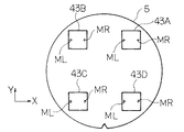
また、既にショットローテーションが発生している恐れのあるときには、所謂ショット内多点EGA方式のアライメントを行うことによって、ウエハ5上の各ショット領域の回転角を実測すればよい。即ち、ショット内多点EGA方式では、図8に示すように、ウエハ5上の各ショット領域内にそれぞれ複数個(例えば2個)の2次元のウエハマークMR及びMLを形成しておく。そして、アライメント時には、ウエハ5上の全部のショット領域から例えば4個のショット領域をサンプルショット43A〜43Dとして選択し、図1のアライメントセンサ34を用いてそれらのサンプルショット43A〜43D内の複数個のウエハマークMR,MLの座標を計測する。この結果を統計処理すると、例えばウエハマークMR及びMLのY座標のずれ量をこれらのX方向の間隔で除算した結果の平均値より、ウエハ5上の各ショット領域の平均的なショットローテーションが求められる。従って、このウエハ5に対して重ね合わせ露光する際には、レチクルを予めそのショットローテーション分だけ回転しておくことによって、重ね合わせ誤差を低減することができる。
【0072】
次に、上記の実施の形態ではレチクルステージ側の非走査方向の移動鏡21Xの曲がりは無視できる程度としていたが、例えば今後ステージの位置決め精度が向上し、且つレチクルステージの走査距離が長くなった場合には、その非走査方向の移動鏡21Xの曲がりの補正を行うことが望ましい。そこで、以下では図9を参照してその移動鏡21Xの曲がりの計測方法、及び補正方法の一例につき説明する。
【0073】
図9(a)は、図2(a)のレチクル微小駆動ステージ11を示し、この図9(a)において、走査方向の移動鏡としてのコーナキューブ21Y1,21Y2のそれぞれのY座標YR1,YR2が計測用ビームLRY1,LRY2によって計測され、非走査方向の移動鏡21Xの2箇所のX座標XR1,XR2が計測用ビームLRX1,LRX2によって計測されている。この際に、レチクル微小駆動ステージ11(レチクル12)の回転補正を(2)式の非走査方向から見た回転角θRXではなく、(4)式の走査方向の回転角θRY(=(YR1−YR2)/L2)に基づいて行う。そして、レチクル微小駆動ステージ11の回転角をその走査方向の回転角θRYが例えば0となるように固定した状態で、レチクル微小駆動ステージ11をY方向に、正確には例えば非走査方向の移動鏡21Xの一方のX座標XR1が一定の値となるように図9(b)の状態まで走査して、レチクル微小駆動ステージ11のY座標YR(=(YR1+YR2)/2)が所定のサンプル座標YRn(n=1,2,…)に達する毎に、移動鏡21Xの2箇所のX座標XR1,XR2の差分ΔXDを求めて記憶する。n番目(n=1,2,3,…)のサンプル点でのX座標XR1,XR2をXR1n,XR2nとすると、n番目の差分ΔXDnは次のようになる。
【0074】
ΔXDn=XR1n−XR2n (14)
この際に、レチクル微小駆動ステージ11のヨーイングは逐次補正されているので、差分ΔXDnは純粋に移動鏡21Xの曲がり情報であり、レチクル微小駆動ステージ11のY座標YRnにおいて、それまでの差分ΔXDnをそれぞれ積分すると共に、それらの中間のY座標YRでは前後の曲がり量を補間することによって、そのY座標YRの関数FD(YR)として移動鏡21Xの曲がり量が求められて、図1の主制御系22A内に記憶される。なお、その移動鏡21Xの曲がり量をスプライン関数等を用いてY座標YRの関数として求めてもよい。
【0075】
即ち、差分ΔXDnの番号nは有限なため、各計測点間の補間を行う必要がある。補間に際して、サンプリング間隔が小さい場合は比例配分でよいが、サンプリング間隔が大きい場合は曲線近似やスプライン関数による補間によって補正の精度を高めることができる。
その後、走査露光を行う際には、レチクル微小駆動ステージ11の移動鏡21Xで実測されるX座標XR(=(XR1+XR2)/2)に対して、その移動鏡21Xの曲がり量FD(YR)を例えば加算することによって、その移動鏡21Xの曲がり量を補正したレチクル微小駆動ステージ11の正確なX座標が求められる。この補正後のX座標を使用することによって、レチクル微小駆動ステージ11(レチクル12)が直線的に走査されるため、ウエハ上に露光されるショット領域の形状が正確な矩形となる。このような移動鏡の曲がりの計測、及び補正はウエハステージ側の移動鏡にも適用できる。
【0076】
なお、上述の実施の形態では、2つの干渉計本体の計測値の平均値を位置として、差分から回転角を求めているが、一方の干渉計本体の計測値を位置として、この位置と他方の干渉計本体の計測値との差分から回転角を求めるようにしてもよい。即ち、一方の干渉計本体を位置計測用として、他方の干渉計本体をヨーイング計測用と明確に分けてもよい。更に、2つの干渉計本体を露光領域等に対して必ずしも対称に配置する必要はない。また、各レーザ干渉計としては、シングルパス方式、ダブルパス方式、又は更に光路を多数回折り返す方式等の何れの方式を使用しても良い。更に、レチクルステージ側の移動鏡曲がりの計測方法は当然にウエハステージ側の移動鏡曲がりの計測に同様に適用することができる。
【0077】
また、上述の実施の形態ではウエハステージには走査方向に2軸、非走査方向に2軸のレーザ干渉計が配置されているが、例えばショット配列の補正を行う必要が無い場合には、走査方向のレーザ干渉計を1軸としてもよい。また、ウエハステージの位置や回転角を求める際の平均化効果を高めるために、走査方向、及び非走査方向に3軸以上のレーザ干渉計を配置するようにしてもよい。同様に、レチクルステージ側でも、非走査方向の移動鏡の曲がり量を計測する必要がなければ、走査方向のレーザ干渉計を1軸としてもよい。また、レチクルステージの位置や回転角を求める際の平均化効果を高めるために、走査方向、及び非走査方向に3軸以上のレーザ干渉計を配置するようにしてもよい。
【0078】
更に本発明は、レチクルステージ及びウエハステージの座標を独立に計測する種々の露光装置にも適用できるものである。このように本発明は上述の実施の形態に限定されず、本発明の要旨を逸脱しない範囲で種々の構成を取り得る。
【0079】
【発明の効果】
本発明の第1の走査型露光装置によれば、基板ステージの非走査方向用の2軸の基板側干渉計の計測値に基づいてその基板ステージとマスクステージとの相対回転角を補正しているため、その基板側干渉計の移動鏡の角度が変化した場合でも、その基板ステージとそのマスクステージとが平行に走査される。従って、感光基板上で露光されるショット領域の形状を所望の形状(矩形等)に維持できる利点がある。そのため、ショット領域の形状の歪に伴う像劣化や、一括露光方式の露光装置とのマッチング誤差が低減される。
【0080】
更に、非走査方向用の2軸の基板側干渉計の計測値の差分と、走査方向用の2軸の基板側干渉計の計測値の差分との差に基づいてその基板ステージの移動方向を補正する移動方向補正手段を設けたため、例えばその基板ステージの非走査方向のステッピング方向を補正することによって、感光基板上に形成されるショット配列を直交格子状にすることができる。これによって重ね合わせ誤差が更に低減される。
【0081】
また、本発明の第2の走査型露光装置によれば、基板ステージの非走査方向の2軸の基板側干渉計の計測値、及びマスクステージの非走査方向の2軸のマスク側干渉計に基づいて、その基板ステージとマスクステージとの相対回転角を補正しているため、そのマスク側干渉計の移動鏡の角度が変化した場合でも、その基板ステージとそのマスクステージとが平行に走査される。従って、感光基板上で露光されるショット領域の形状を所望の形状(矩形等)に維持できる利点がある。
【0082】
また、本発明の第3の走査型露光装置によれば、複数軸のマスク側干渉計の測定値を用いることによって、マスクステージの走査中にそのマスクステージの回転角を測定できる。従って、そのマスクステージの回転角を例えばその基板ステージの走査方向に応じて制御することによって、その基板上に露光されるショット領域の形状を目標とする形状に維持できる。
また、本発明の実施の形態に記載された走査型露光装置によれば、一方のステージの第1の2軸の干渉計の計測値の差分に基づいてそのステージの回転角を検出し、この検出結果、及び第2の2軸の干渉計の計測値の差分に基づいてこの第2の2軸の干渉計用の移動鏡の曲がり量を算出しているため、そのステージにヨーイングが生じていてもその移動鏡の曲がり量を正確に検出できる。従って、実際の走査露光時にはその移動鏡の曲がり量を補正しながらそのステージの走査を行うことによって、そのステージを所望の方向に正確に走査できるため、感光基板上で露光されるショット領域の形状を所望の形状に維持できる利点がある。
【0083】
これらの場合において、その基板ステージ、及びそのマスクステージの一方のステージの走査方向に直交する非走査方向の位置を計測する2軸の干渉計の計測値の差分が所定の閾値を超えた際に、そのマスクとその基板ステージとの位置関係を計測する計測手段を更に備えた場合には、感光基板上でのショット領域の形状誤差が減少する利点がある。
【図面の簡単な説明】
【図1】本発明による走査型露光装置の実施の形態の一例を示す概略構成図である。
【図2】(a)は図1の投影露光装置のレチクルステージ側の干渉計の配置を示す平面図、(b)は図1の投影露光装置のウエハステージ側の干渉計の配置を示す平面図である。
【図3】本発明の実施の形態において、ウエハステージ側の移動鏡の傾きが変化した場合のショット領域の形状、及びショット配列を示す説明図である。
【図4】図3の構成でマスクステージ側の移動鏡の傾きが変化した場合のショット領域の形状、及びショット配列を示す説明図である。
【図5】従来技術と同じ構成でマスクステージ側の移動鏡の傾きが変化した場合のショット領域の形状、及びショット配列を示す説明図である。
【図6】図3の構成に対してマスクステージ側でも回転角を非走査方向の2軸の干渉計で計測するようにした場合のショット領域の形状、及びショット配列を示す説明図である。
【図7】本発明の実施の形態において、ウエハステージ及びマスクステージの両方で回転角を非走査方向の2軸の干渉計で計測するようにして、マスクステージ側の移動鏡の傾きが変化した場合のショット領域の形状、及びショット配列を示す説明図である。
【図8】ショット内多点EGA方式で使用されるウエハマークの一例を示す平面図である。
【図9】レチクル微小駆動ステージ11上の非走査方向の移動鏡21Xの曲がり量の計測方法の説明図である。
【図10】従来技術でウエハステージ側の移動鏡の傾きが変化した場合のショット領域の形状、及びショット配列を示す説明図である。
【符号の説明】
4 Zθ軸駆動ステージ
5 ウエハ
6 基準マーク板
7X,7Y ウエハステージ側の移動鏡
8 投影光学系
11 レチクル微小駆動ステージ
12 レチクル
13X1,13X2,13Y1,13Y2 干渉計本体
14X1,14X2,14Y1,14Y2 干渉計本体
19,20 レチクルアライメント顕微鏡
21X レチクルステージ側の移動鏡
21Y1,21Y2 コーナキューブ
22A 主制御系
22D レチクル駆動装置[0001]
BACKGROUND OF THE INVENTION
The present invention relates to an exposure used for transferring a mask pattern onto a photosensitive substrate in a photolithography process for manufacturing, for example, a semiconductor element, an imaging element (CCD, etc.), a liquid crystal display element, or a thin film magnetic head. More particularly, the present invention relates to a scanning exposure type exposure apparatus (scanning type exposure apparatus) such as a step-and-scan method.
[0002]
[Prior art]
For example, when a semiconductor device is manufactured, a part of the pattern on the reticle is projected onto the wafer via the projection optical system, and the reticle and the wafer are scanned synchronously with respect to the projection optical system. A so-called step-and-scan projection exposure apparatus that sequentially transfers the pattern image to each shot area on the wafer is used.
[0003]
In such a step-and-scan method, since a projection optical system with a normal reduction magnification is used, it is necessary to independently drive the reticle stage and the wafer stage at a speed ratio corresponding to the reduction magnification, and each shot. Since the movement between the regions is performed by a stepping method, the mechanism of the stage system is complicated, and extremely high control is required (for example, see Japanese Patent Application Laid-Open No. 7-176468).
[0004]
Therefore, as shown in FIG. 10, the speed and position of the stage of the step-and-scan type projection exposure apparatus are conventionally controlled based on the measurement value of the laser interferometer. That is, in FIGS. 10A1 and 10A2, the
[0005]
At this time, the Y coordinate in the scanning direction is represented by the average value of the biaxial laser interferometer, and the rotation of the wafer stage 51 (wafer W) and the reticle stage 54 (reticle R) is further determined by the difference between the biaxial Y coordinates. The angle is measured, and at the time of scanning exposure, the X and Y coordinates of both
[0006]
That is, at the time of scanning exposure, assuming that the reflecting surface of the movable mirror is exactly parallel to the X axis and the Y axis, the wafer W is moved in the −Y direction with respect to the slit-
[0007]
On the other hand, when the
[0008]
[Problems to be solved by the invention]
As described above, in the conventional step-and-scan type projection exposure apparatus, the coordinate position of the wafer stage and the reticle stage is measured by the laser interferometer, and the orthogonality of the two-axis moving mirror for the laser interferometer is good. In some cases, even if the wafer stage is rotated by yawing, the shape of the shot area to be exposed is a rectangle, and the resulting shot arrangement is also an orthogonal lattice.
[0009]
However, the stage is thermally deformed by the temperature change of the atmospheric gas or the temperature rise by exposure light irradiation, or the movable mirror for the laser interferometer itself is thermally deformed. When the degree is deteriorated, the shape of the shot area to be exposed is not rectangular, and the shot arrangement may not be orthogonal lattice. This is mainly because, conventionally, the position of the stage in the scanning direction is measured by a biaxial laser interferometer, and the rotation angle of the stage is obtained by the difference between the obtained measurement values. In other words, in the example of FIG. This is considered to be due to the fact that the laser beam from the laser interferometer for yawing measurement was irradiated to the
[0010]
Specifically, FIG. 10C1 shows a state where the
[0011]
FIG. 10D1 shows a state in which the
[0012]
Since the arrangement error of the shot arrangement shown in FIG. 10 (c4) or (d4) is a linear error (primary error), when performing exposure on the layer above it, for example, so-called enhanced global alignment ( EGA) alignment is performed, a shot arrangement is obtained by statistical processing, and the wafer stage is stepped according to the obtained shot arrangement, thereby substantially correcting the arrangement error. However, when the shape of the shot area is deformed as indicated by the shot areas SAc and SAd, the width in the Y direction of the slit-shaped
[0013]
In addition, since exposure is performed by a so-called mix-and-match method, it is also possible to perform overlay exposure using a batch exposure type exposure apparatus such as a stepper on a deformed shot region such as the shot regions SAc and SAd. The exposure type cannot be corrected in accordance with such a deformed shot shape. Therefore, such a deformed shot region includes a distortion error, and there is a disadvantage that matching accuracy is deteriorated.
[0014]
Furthermore, not only when the tilt of the moving mirror of the laser interferometer changes, but also when the moving mirror has a bend along the scanning direction, there is a disadvantage that the shape of the shot area to be exposed is distorted.
In view of this point, the present invention is a scanning type capable of maintaining the shape of a shot area exposed on a photosensitive substrate in a desired shape even when the angle of a moving mirror of an interferometer for measuring the position of the stage changes. It is a first object to provide an exposure apparatus.
[0015]
A second object of the present invention is to provide a scanning exposure apparatus that can maintain the shape of a shot area exposed on a photosensitive substrate in a desired shape even when the movable mirror is bent.
[0016]
[Means for Solving the Problems]
A first scanning exposure apparatus according to the present invention includes a mask stage (9 to 11) that moves a mask (12) on which a transfer pattern is formed, and a substrate stage (1) that moves a photosensitive substrate (5). 4), and in a state in which the mask is illuminated with illumination light for exposure, the substrate (5) is scanned in a predetermined direction through the substrate stage, and is synchronized with the mask stage. In a scanning exposure apparatus that sequentially transfers the pattern of the mask (12) onto the substrate (5) by scanning the mask (12) in a direction corresponding to the predetermined direction, the scanning direction (Y direction) of the substrate stage The position ofTwo axes measured at two locations along the non-scanning direction orthogonal to the scanning directionSubstrate side interferometer (13Y1,13Y2,7Y) and the substrate stageThatA biaxial substrate side interferometer (13X1, 13X2, 7X) that measures the position in the non-scanning direction (X direction) at two locations along the scanning direction;ThatRotation angle correction means (22D, 44R, 44L) for correcting the relative rotation angle between the substrate stage and the mask stage based on the measurement value of the biaxial substrate side interferometer for the non-scanning direction;The movement direction of the substrate stage based on the difference between the measurement value of the two-axis substrate side interferometer for the non-scanning direction and the difference of the measurement value of the two-axis substrate side interferometer for the scanning direction Direction correction means (22A, 22B) for correctingIt is what has.
[0017]
According to the present invention, for example, as shown in FIG. 2, the biaxial interferometer body (13X1) faces the moving mirror (7X) for the non-scanning direction of the substrate stage for moving the substrate (5). 13X2), the coordinates are determined by the average value of the two axes, and the yawing amount (rotation angle) in the non-scanning direction of the substrate stage is obtained from the difference between the measurement values of these two axes. In response, the mask (12) is rotated. The rotation angle of the mask stage at this time can be obtained from the difference between the measurement values of a biaxial interferometer arranged in either the scanning direction or the non-scanning direction, for example.
[0018]
As a result, for example, as shown in FIGS. 3C1 to 3C4, when the angle of the movable mirror (7X) in the non-scanning direction of the substrate stage changes, the substrate (5) and the mask (12) have the same angle. Therefore, the shot area (SA3) exposed on the substrate (5) remains rectangular even if it is rotated. For example, as shown in FIGS. 3 (d1) to (d4), when the angle of the movable mirror (7Y) in the scanning direction of the substrate stage changes, both the substrate (5) and the mask (12) are inclined. The shot area (SA4) exposed on the substrate (5) remains rectangular because it is scanned without any change. That is, according to the present invention, since the scanning direction of the substrate (5) and the mask (12) is always the same, the shape of the shot area exposed on the substrate (5) is maintained at the target shape.
[0019]
Thus, even if the shape of the shot region becomes the target shape, as shown in FIG. 3 (c4) or (d4), the shot arrangement is not an orthogonal lattice (a lattice in which the arrangement directions are orthogonal). This shot arrangement is further made into an orthogonal lattice shape.For thatThe difference (yaw amount) between the measurement values of the biaxial substrate side interferometers (13X1, 13X2, 7X) for the non-scanning direction and the biaxial substrate side interferometers (13Y1, 13Y2, 7Y) for the scanning direction Movement direction correction means (22A, 22B) for correcting the movement direction of the substrate stage based on the difference between the measurement values (the amount of yawing).Is provided.
[0020]
At this time, if, for example, the stepping direction in the non-scanning direction of the substrate stage is corrected using the difference between the yawing amount in the non-scanning direction measured by the present invention and the yawing amount in the scanning direction, for example, FIG. The shot arrangement shown in c4) or (d4) has an orthogonal lattice shape indicated by a dotted line.
Next, the case where the movable mirror (21X, 21Y) on the mask stage side is inclined and the orthogonality is deteriorated will be considered. Also in this case, as in the conventional example, the position of the movable mirror (21Y) for the scanning direction of the mask stage is measured with a two-axis interferometer, and the mask stage is measured based on the difference between the measured values of these two axes. When the rotation angle is controlled, the shape of the shot area to be exposed may not be rectangular.
[0021]
That is, FIGS. 4 (a2) and (b2), and FIGS. 5 (a2) and (b2) are arranged with a biaxial interferometer body facing the movable mirror (21Y) for the scanning direction of the mask stage, respectively. An example is shown in which a uniaxial interferometer body is disposed facing a movable mirror (21X) for the non-scanning direction. 4 (a1) and 4 (a2) show an example in which the position of the substrate stage in the non-scanning direction is measured by a biaxial interferometer as in the first scanning exposure apparatus of the present invention, and FIG. ) And (a2) show an example in which the position of the substrate stage in the scanning direction is measured by a biaxial interferometer as in the conventional example.
[0022]
In these cases, as shown in FIG. 4 (a2) or FIG. 5 (a2), if the movable mirror (21Y) in the scanning direction of the mask stage is inclined by an angle θ with respect to the mask (12), the movement is performed. Since the mirror (21Y) is scanned so as to be parallel to the substrate stage, as indicated by arrows (37a, 38a), the mask (12) is rotated with respect to the scanning direction of the substrate (5). Scanned at an angle. Accordingly, the shape of the shot area (SA5, SA7) to be exposed is a shape obtained by rotating the parallelogram by 90 °. On the other hand, as shown in FIG. 4 (b2) or FIG. 5 (b2), when the movable mirror (21X) in the non-scanning direction of the mask stage is inclined by the angle θ with respect to the mask (12). Since the movable mirror (21Y) is scanned so as to be parallel to the substrate stage, the scanning direction of the mask (12) is set to the scanning direction of the substrate (5) as indicated by arrows (37b, 38b). The shape of shot areas (SA6, SA8) which are inclined and exposed is a parallelogram.
[0023]
Therefore, in order to avoid such deformation of the shot area, the second scanning exposure apparatus according to the present invention includes a mask stage (9 to 11) that moves a mask (12) on which a transfer pattern is formed, and a photosensitive element. The substrate (5) is moved in a predetermined direction through the substrate stage in a state where the mask (12) is illuminated with illumination light for exposure. In synchronization with scanning in the (Y direction), the mask (12) is scanned on the substrate (5) by scanning the mask (12) in the direction (Y direction) corresponding to the predetermined direction through the mask stage. In the scanning type exposure apparatus that sequentially transfers the pattern of 2), a biaxial substrate side interferometer that measures the position in the non-scanning direction (X direction) orthogonal to the scanning direction of the substrate stage at two locations along the scanning direction. (13X1, 13X , 7X), and a biaxial mask side interferometer (14X1, 14X2, 21X) that measures positions in a non-scanning direction orthogonal to the scanning direction of the mask stage at two locations along the scanning direction of the mask stage; Rotation angle correction means (22D, 44R) that corrects the relative rotation angle between the substrate stage and the mask stage based on the measurement value of the biaxial substrate side interferometer and the measurement value of the biaxial mask side interferometer. 44L).
[0024]
According to the present invention, for example, as shown in FIG. 7, the position of the movable mirror (7X) in the non-scanning direction of the substrate stage is measured by the biaxial interferometer, and the movable mirror (in the non-scanning direction of the mask stage) 21X) is also measured by a two-axis interferometer, and the yawing amount of the substrate stage is obtained from the difference between the two measurement values of the movable mirror (7X), and the two measurement values of the movable mirror (21X) are obtained. The rotation angle of the mask stage is obtained from the difference. Accordingly, as shown in FIG. 7 (a2) or (b2), either the moving mirror (21Y) in the scanning direction on the mask stage side or the moving mirror (21X) in the non-scanning direction is against the mask (12). Even when tilted, the scanning direction of the mask (12) is parallel to the scanning direction of the substrate (5), and the shape of the exposed shot areas (SA13, SA14) is rectangular even if rotation (shot rotation) occurs. Become.
[0025]
next,Described in the embodiment of the present inventionThe scanning exposure apparatus has a mask stage (9 to 11) that moves a mask (12) on which a transfer pattern is formed, and a substrate stage (1 to 4) that moves a photosensitive substrate (5). Then, in a state where the mask (12) is illuminated with the illumination light for exposure, the substrate (5) is scanned in the predetermined direction (Y direction) via the substrate stage, and is synchronized with the mask stage via the mask stage. In a scanning exposure apparatus that sequentially transfers a pattern of a mask (12) onto a substrate (5) by scanning the mask (12) in a direction (Y direction) corresponding to the predetermined direction, the substrate stage, and the A first biaxial interferometer (14Y1, 14Y2, 21Y) that measures the position in the scanning direction of one stage (9-11) of the mask stage at two locations along the non-scanning direction orthogonal to the scanning direction; One of them The second biaxial interferometer (14X1, 14X2, 21X) that measures the position of the stage in the non-scanning direction at two locations along the scanning direction of the stage, and the measurement of the first biaxial interferometer The rotation angle of the one stage is detected based on the difference between the values, and the detection result and the difference between the measurement values of the second two-axis interferometer are used for the second two-axis interferometer. Mobile mirror bending amount calculation means (22A) for calculating the bending amount of the movable mirror (21X).
[0026]
According to the present invention, for example, a biaxial interferometer (14Y1, 14Y2, 21Y) is arranged for measuring the position of the mask stage in the scanning direction, and a biaxial interferometer (14Y1, 14Y2, 21Y) is used for measuring the position in the non-scanning direction. 14X1, 14X2, 21X), for example, as shown in FIG. 9, when the moving mirror (21X) of the interferometer in the non-scanning direction is bent, the mask (12) is scanned while being bent. The shot area may be distorted. Therefore, when the mask stage is moved in the scanning direction, the difference between the measurement values of the two-axis interferometer in the scanning direction is made constant so that yawing of the mask stage does not occur. In this state, when the difference between the measurement values of the two-axis interferometer for the non-scanning direction is monitored, the bent shape of the movable mirror (21X) in the non-scanning direction can be measured. During actual scanning exposure, the mask stage moves linearly in the scanning direction by correcting the measurement value of the two-axis interferometer by the amount of bending of the movable mirror (21X) thus measured. A shot area closer to a rectangle is exposed.
[0027]
In each scanning exposure apparatus of the present invention described above, the difference between the measurement values of the biaxial interferometer that measures the position in the non-scanning direction orthogonal to the scanning direction of one of the substrate stage and the mask stage. And measuring means (6, 19, 20) for measuring the positional relationship between the mask (12) and the substrate stage when the monitored difference exceeds a predetermined threshold. desirable. The reason why the difference between the measurement values of the two-axis interferometers exceeds the predetermined threshold is presumably because the tilt angle of the interferometer moving mirror has changed greatly due to thermal deformation or the like. At this time, by re-measuring the positional relationship between the mask (12) and the substrate stage, the positional relationship between the mask (12) and the substrate (5) can be corrected, thereby reducing the shape error of the shot region to be exposed. To do. In such a case, since the amount of bending of the movable mirror may be changed, the amount of bending of the movable mirror may be measured again.
Next, according to the present inventionThirdThe scanning exposure apparatus includes a mask stage (9 to 11) that holds and moves a mask (12) on which a transfer pattern is formed, and a substrate stage (1 that holds and moves a photosensitive substrate (5). 4), and the mask stage and the substrate stage are scanned synchronously at different speeds in opposite directions along the scanning direction in a state where the mask is illuminated with illumination light for exposure. Thus, in the scanning type exposure apparatus that sequentially transfers the mask pattern onto the substrate, the position of the mask stage in the non-scanning direction perpendicular to the scanning direction is set at a plurality of locations separated along the scanning direction. A plurality of mask-side interferometers (14X1, 14X2, and 21X) for measuring, the mask-side interferometer being in the non-moving state while the mask stage is moving in the scanning direction; The position of the mask stage in 査 direction, while simultaneously measured at the plurality of locations, and outputs the measured value for each measurement axis.
According to the present invention, the rotation angle of the mask stage can be measured during the scanning of the mask stage by using the measurement values of the multi-axis mask side interferometer. Therefore, by controlling the rotation angle of the mask stage according to the scanning direction of the substrate stage, for example, the shape of the shot area exposed on the substrate can be maintained at the target shape.
The present invention further includes rotation angle correction means (22D, 44R, 44L) for correcting the relative rotation angle between the substrate stage and the mask stage based on the measurement values of the multi-axis mask side interferometer. Also good. By using the rotation angle correction means, for example, by making the scanning direction of the mask and the substrate the same, the shape of the shot area exposed on the substrate can be maintained at the target shape.
The substrate stage further includes a multi-axis substrate-side interferometer (13X1, 13X2, 7X) that measures the position of the substrate stage in the non-scanning direction orthogonal to the scanning direction at a plurality of locations separated along the scanning direction. The substrate-side interferometer measures the position of the substrate stage in the non-scanning direction at the same time at the plurality of locations while the substrate stage is moving in the scanning direction. The measured value may be output to
Further, a rotation angle correction means (22D) that corrects the relative rotation angle between the substrate stage and the mask stage based on the measurement value of the multi-axis substrate side interferometer and the measurement value of the multi-axis mask side interferometer. , 44R, 44L).
[0028]
DETAILED DESCRIPTION OF THE INVENTION
Hereinafter, an embodiment of a scanning exposure apparatus according to the present invention will be described with reference to the drawings. In this example, the present invention is applied to a step-and-scan projection exposure apparatus.
FIG. 1 shows a projection exposure apparatus of this example. In FIG. 1, a rectangular illumination area (hereinafter referred to as “slit illumination area”) by exposure light EL from an illumination optical system not shown in FIG. The pattern is illuminated, and an image of the pattern is projected onto the
[0029]
Next, the
[0030]
On the other hand, a wafer Y-
[0031]
As will be described later, a wafer coordinate system defined by coordinates measured by the
[0032]
Above the
[0033]
Next, the configuration of the interferometer for the stage system (interference type length measuring device) of this example will be described with reference to FIG.
2A is a plan view showing the reticle
[0034]
Since the reticle 12 (reticle microdrive stage 11) is scanned in the Y direction, the
[0035]
XR = (XR1 + XR2) / 2 (1)
θRX= (XR1-XR2) / L1 (2)
Further, corner cubes 21Y1 and 21Y2 as moving mirrors are fixed at the end in the + Y direction of the
[0036]
The measurement beams LRY1 and LRY2 are also distributed symmetrically in the X direction with respect to the center (optical axis AX) of the
[0037]
YR = (YR1 + YR2) / 2 (3)
θRY= (YR1-YR2) / L2 (4)
ΔωR = (YR1-YR2) / L2- (XR1-XR2) / L1 (5)
In this example, normally, the rotation angle θ viewed from the non-scanning direction of equation (2)RXBased on the above, the rotation angle (yawing amount) of the
[0038]
2A, the moving
[0039]
Next, in FIG. 2B, a
[0040]
Further, an image of a part of the pattern of the
[0041]
The
[0042]
XW = (XW1 + XW2) / 2 (6)
YW = (YW1 + YW2) / 2 (7)
θWX= (XW1-XW2) / L3 (8)
ΔωW = (YW1-YW2) / L4- (XW1-XW2) / L3 (9)
In FIG. 2B, the moving
[0043]
Next, basic operations when performing alignment, scanning exposure, and stepping in the projection exposure apparatus of this example will be described. First, reticle alignment is performed using the
[0044]
In addition, the scanning direction of the Zθ-
[0045]
Next, the stage on the wafer stage side and the stage on the reticle stage side are synchronously scanned in the same manner as in scanning exposure without irradiating exposure light, and the reticles corresponding to the reference marks 46C to 46F on the
[0046]
In this case, the movement of each stage is based on the guide surface of each stage. At the time of assembly adjustment of the projection exposure apparatus, for example, the parallelism between the guide surface of the reticle Y-
[0047]
When the amount of positional deviation between the outer shape of the
[0048]
Next, wafer alignment is performed to determine the arrangement of the shot areas on the
[0049]
Thereafter, a scanning exposure operation is performed in accordance with the coordinate system (XW, YW) of the wafer stage and the coordinate system (XR, YR) of the reticle stage determined at the time of the previous reticle alignment. The coordinate system is based on each of the
[0050]
That is, the coordinates of the reticle stage coordinate system (XR, YR) when the shot area to be exposed and the reticle are aligned by wafer alignment are set to (XR0, YR0), The coordinates of the coordinate system (XW, YW) of the wafer stage (XW0YW0), Since the projection magnification of the projection optical system 8 is 1 / M, the subsequent scanning direction of the reticle micro-driving stage 11 (reticle 12) and the Zθ-axis driving stage 4 (wafer 5) and the non-scanning direction The synchronization errors ΔX and ΔY can be expressed as follows. However, these synchronization errors are errors converted on the
[0051]
ΔX = (XW−XW0) ・ M- (XR-XR0(10)
ΔY = (YW−YW0) ・ M- (YR-YR0(11)
In this example, the rotation angle θ of the Zθ-
[0052]
[0053]
Thereafter, when performing stepping of the
[0054]
Further, when the orthogonality error ΔωW of the equation (9) or the orthogonality error ΔωR of the equation (5) greatly changes beyond a predetermined allowable value, the baseline amount of the other off-axis
[0055]
Next, a specific example of the shape of a shot area obtained by performing scanning exposure with the projection exposure apparatus of this example and a shot arrangement will be described.
First, the case where the orthogonality of the reticle stage side movable mirror shown in FIG. 2 is good and the inclination of the wafer stage side
[0056]
FIGS. 3 (a1) to 3 (d1) simply show the
[0057]
In FIG. 3, it is assumed that the contour of the pattern area of the
[0058]
Δθ ′ = θWX−θRY (13)
As shown in FIG. 3A1, the orthogonality of the
[0059]
Next, as shown in FIG. 3B1, when the orthogonality of the
[0060]
On the other hand, as shown in FIG. 3C1, when the angle of the moving
[0061]
On the other hand, as shown in FIG. 3D1, when the angle of the moving
[0062]
Although FIG. 3 shows the case where the rotation angle of the
FIG. 6 shows a case where the rotational angle of the
[0063]
Further, even if the moving
[0064]
Next, the case where the
[0065]
As shown in FIG. 4 (a2), when the moving
[0066]
FIG. 5 shows a conventional technique, that is, a case where the rotation angle of the
[0067]
As described above, when the rotation angle of the reticle micro-drive stage 11 (reticle 12) is corrected based on the rotation angle of the
[0068]
FIG. 7 shows a case where the rotation angle of the
[0069]
As described above, according to this example, since the rotation angle of the
[0070]
However, even if the shot arrangement is an orthogonal lattice, for example, as shown in FIG. 7B2, when the
[0071]
When there is a possibility that shot rotation has already occurred, the rotation angle of each shot area on the
[0072]
Next, in the above embodiment, the bending of the
[0073]
FIG. 9A shows the reticle
[0074]
ΔXDn = XR1n−XR2n (14)
At this time, since the yawing of the
[0075]
That is, since the number n of the difference ΔXDn is finite, it is necessary to perform interpolation between each measurement point. In interpolation, proportional distribution may be used when the sampling interval is small, but when the sampling interval is large, the accuracy of correction can be improved by curve approximation or interpolation using a spline function.
Thereafter, when performing scanning exposure, the bending amount FD (YR) of the
[0076]
In the above-described embodiment, the rotation angle is obtained from the difference with the average value of the measurement values of the two interferometer bodies as the position. However, the position and the other value are determined with the measurement value of one interferometer body as the position. The rotation angle may be obtained from the difference from the measured value of the interferometer body. That is, one interferometer body may be clearly divided for position measurement and the other interferometer body may be clearly divided for yawing measurement. Further, the two interferometer bodies need not necessarily be arranged symmetrically with respect to the exposure area or the like. Further, as each laser interferometer, any method such as a single-pass method, a double-pass method, or a method that diffracts a large number of optical paths may be used. Furthermore, the method for measuring the moving mirror bend on the reticle stage side can naturally be similarly applied to the measurement of the moving mirror bend on the wafer stage side.
[0077]
In the above-described embodiment, the biaxial laser interferometer is arranged on the wafer stage in the scanning direction and the biaxial in the non-scanning direction. For example, when it is not necessary to correct the shot arrangement, the scanning is performed. The direction laser interferometer may be uniaxial. Further, in order to enhance the averaging effect when obtaining the position and rotation angle of the wafer stage, a laser interferometer having three or more axes may be arranged in the scanning direction and the non-scanning direction. Similarly, on the reticle stage side, if it is not necessary to measure the amount of bending of the movable mirror in the non-scanning direction, the laser interferometer in the scanning direction may be uniaxial. Further, in order to enhance the averaging effect when obtaining the position and rotation angle of the reticle stage, a laser interferometer having three or more axes may be arranged in the scanning direction and the non-scanning direction.
[0078]
Further, the present invention can be applied to various exposure apparatuses that independently measure the coordinates of the reticle stage and the wafer stage. As described above, the present invention is not limited to the above-described embodiment, and various configurations can be taken without departing from the gist of the present invention.
[0079]
【The invention's effect】
According to the first scanning exposure apparatus of the present invention, the relative rotation angle between the substrate stage and the mask stage is corrected based on the measurement value of the biaxial substrate side interferometer for the non-scanning direction of the substrate stage. Therefore, even when the angle of the movable mirror of the substrate side interferometer changes, the substrate stage and the mask stage are scanned in parallel. Therefore, there is an advantage that the shape of the shot area exposed on the photosensitive substrate can be maintained in a desired shape (rectangular shape or the like). For this reason, image degradation due to distortion of the shape of the shot area and matching errors with a batch exposure type exposure apparatus are reduced.
[0080]
MoreThe movement direction of the substrate stage is corrected based on the difference between the measurement value of the two-axis substrate side interferometer for the non-scanning direction and the difference of the measurement value of the two-axis substrate side interferometer for the scanning direction. Provided moving direction correction means toForFor example, by correcting the stepping direction of the substrate stage in the non-scanning direction, the shot arrangement formed on the photosensitive substrate can be made into an orthogonal lattice. This further reduces the overlay error.
[0081]
Further, according to the second scanning exposure apparatus of the present invention, the measurement value of the biaxial substrate side interferometer in the non-scanning direction of the substrate stage and the biaxial mask side interferometer in the non-scanning direction of the mask stage are used. Since the relative rotation angle between the substrate stage and the mask stage is corrected based on this, the substrate stage and the mask stage are scanned in parallel even if the angle of the movable mirror of the mask interferometer changes. The Therefore, there is an advantage that the shape of the shot area exposed on the photosensitive substrate can be maintained in a desired shape (rectangular shape or the like).
[0082]
According to the third scanning exposure apparatus of the present invention,By using the measurement values of the multi-axis mask side interferometer, the rotation angle of the mask stage can be measured during scanning of the mask stage. Therefore, by controlling the rotation angle of the mask stage according to the scanning direction of the substrate stage, for example, the shape of the shot area exposed on the substrate can be maintained at the target shape.
Further, according to the scanning exposure apparatus described in the embodiment of the present invention,The rotation angle of the stage is detected based on the difference between the measurement values of the first two-axis interferometer of one stage, and based on the detection result and the difference between the measurement values of the second two-axis interferometer. Since the bending amount of the movable mirror for the second two-axis interferometer is calculated, the bending amount of the movable mirror can be accurately detected even if yawing occurs on the stage. Therefore, since the stage can be scanned accurately in a desired direction by correcting the amount of bending of the movable mirror during actual scanning exposure, the shape of the shot area exposed on the photosensitive substrate Can be maintained in a desired shape.
[0083]
In these cases, when the difference between the measurement values of the two-axis interferometer that measures the position in the non-scanning direction orthogonal to the scanning direction of the substrate stage and one of the mask stages exceeds a predetermined threshold value. Further, when the measuring means for measuring the positional relationship between the mask and the substrate stage is further provided, there is an advantage that the shape error of the shot area on the photosensitive substrate is reduced.
[Brief description of the drawings]
FIG. 1 is a schematic block diagram showing an example of an embodiment of a scanning exposure apparatus according to the present invention.
2A is a plan view showing the arrangement of interferometers on the reticle stage side of the projection exposure apparatus of FIG. 1, and FIG. 2B is a plane showing the arrangement of interferometers on the wafer stage side of the projection exposure apparatus of FIG. FIG.
FIG. 3 is an explanatory diagram showing the shape of a shot area and the shot arrangement when the tilt of a moving mirror on the wafer stage side changes in the embodiment of the present invention.
4 is an explanatory diagram showing the shape of a shot area and the shot arrangement when the inclination of the movable mirror on the mask stage side changes in the configuration of FIG. 3;
FIG. 5 is an explanatory diagram showing the shape of a shot area and the shot arrangement when the inclination of the movable mirror on the mask stage side changes with the same configuration as in the prior art.
6 is an explanatory diagram showing the shape of a shot area and the shot arrangement when the rotation angle is measured with a biaxial interferometer in the non-scanning direction on the mask stage side as compared with the configuration of FIG. 3;
FIG. 7 shows that the tilt of the movable mirror on the mask stage side is changed by measuring the rotation angle with a biaxial interferometer in the non-scanning direction in both the wafer stage and the mask stage in the embodiment of the present invention. It is explanatory drawing which shows the shape of a shot area | region, and a shot arrangement | sequence in a case.
FIG. 8 is a plan view showing an example of a wafer mark used in the in-shot multipoint EGA method.
FIG. 9 is an explanatory diagram of a method of measuring the amount of bending of the
FIG. 10 is an explanatory diagram showing the shape of a shot area and the shot arrangement when the tilt of the moving mirror on the wafer stage side is changed in the prior art.
[Explanation of symbols]
4 Zθ axis drive stage
5 Wafer
6 Reference mark plate
7X, 7Y Wafer stage side moving mirror
8 Projection optical system
11 Reticle micro-drive stage
12 Reticles
13X1, 13X2, 13Y1, 13Y2 Interferometer body
14X1, 14X2, 14Y1, 14Y2 Interferometer body
19, 20 Reticle alignment microscope
21X Reticle stage side moving mirror
21Y1,21Y2 Corner cube
22A Main control system
22D reticle drive
Claims (7)
前記基板ステージの走査方向の位置を、該走査方向に直交する非走査方向に沿った2箇所で計測する2軸の基板側干渉計と、
前記基板ステージの前記非走査方向の位置を前記走査方向に沿った2箇所で計測する2軸の基板側干渉計と、
前記非走査方向用の2軸の基板側干渉計の計測値に基づいて前記基板ステージと前記マスクステージとの相対回転角を補正する回転角補正手段と、
前記非走査方向用の2軸の基板側干渉計の計測値の差分と、前記走査方向用の2軸の基板側干渉計の計測値の差分との差に基づいて、前記基板ステージの移動方向を補正する移動方向補正手段と、を有することを特徴とする走査型露光装置。A mask stage that moves a mask on which a transfer pattern is formed and a substrate stage that moves a photosensitive substrate, and the mask is illuminated with illumination light for exposure through the substrate stage. A scanning type that sequentially transfers the mask pattern onto the substrate by scanning the mask in a direction corresponding to the predetermined direction through the mask stage in synchronization with scanning the substrate in a predetermined direction. In the exposure apparatus,
A biaxial substrate-side interferometer that measures the position of the substrate stage in the scanning direction at two locations along the non-scanning direction orthogonal to the scanning direction ;
A biaxial substrate-side interferometer that measures the position of the substrate stage in the non-scanning direction at two locations along the scanning direction;
A rotational angle correction means for correcting the relative rotation angle between the substrate stage and the mask stage based on the measurement values of the substrate-side interferometers 2 axes for the non-scanning direction,
Based on the difference between the measurement value of the two-axis substrate side interferometer for the non-scanning direction and the difference of the measurement value of the two-axis substrate side interferometer for the scanning direction, the movement direction of the substrate stage A scanning direction exposure apparatus comprising: a moving direction correcting unit that corrects
前記基板ステージの走査方向に直交する非走査方向の位置を前記走査方向に沿った2箇所で計測する2軸の基板側干渉計と、
前記マスクステージの走査方向に直交する非走査方向の位置を前記マスクステージの走査方向に沿った2箇所で計測する2軸のマスク側干渉計と、
前記2軸の基板側干渉計の計測値及び前記2軸のマスク側干渉計の計測値に基づいて前記基板ステージと前記マスクステージとの相対回転角を補正する回転角補正手段と、を有することを特徴とする走査型露光装置。A mask stage that moves a mask on which a transfer pattern is formed and a substrate stage that moves a photosensitive substrate, and the mask is illuminated with illumination light for exposure through the substrate stage. A scanning type that sequentially transfers the mask pattern onto the substrate by scanning the mask in a direction corresponding to the predetermined direction through the mask stage in synchronization with scanning the substrate in a predetermined direction. In the exposure apparatus,
A biaxial substrate-side interferometer that measures the position in the non-scanning direction orthogonal to the scanning direction of the substrate stage at two locations along the scanning direction;
A biaxial mask-side interferometer that measures a position in a non-scanning direction orthogonal to the scanning direction of the mask stage at two locations along the scanning direction of the mask stage;
Rotation angle correction means for correcting a relative rotation angle between the substrate stage and the mask stage based on the measurement value of the biaxial substrate side interferometer and the measurement value of the biaxial mask side interferometer. A scanning exposure apparatus characterized by the above.
前記マスクステージの、前記走査方向に直交する非走査方向の位置を、前記走査方向に沿って離れた複数箇所で計測する複数軸のマスク側干渉計を有し、
前記マスク側干渉計は、前記マスクステージが前記走査方向に移動している最中に、前記非走査方向における前記マスクステージの位置を、前記複数箇所で同時に測定すると共に、各計測軸毎にその測定値を出力することを特徴とする走査型露光装置。A mask stage that holds and moves a mask on which a pattern for transfer is formed and a substrate stage that holds and moves a photosensitive substrate, and the mask is illuminated with exposure illumination light, In the scanning exposure apparatus for sequentially transferring the mask pattern onto the substrate by scanning the mask stage and the substrate stage synchronously at different speeds in opposite directions along the scanning direction, respectively.
A multi-axis mask side interferometer that measures the position of the mask stage in a non-scanning direction orthogonal to the scanning direction at a plurality of locations separated along the scanning direction;
While the mask stage is moving in the scanning direction, the mask side interferometer measures the position of the mask stage in the non-scanning direction simultaneously at the plurality of locations, and for each measurement axis, A scanning exposure apparatus that outputs a measured value.
前記基板側干渉計は、前記基板ステージが前記走査方向に移動している最中に、前記非走査方向における前記基板ステージの位置を、前記複数箇所で同時に測定すると共に、各計測軸毎にその測定値を出力することを特徴とする請求項4に記載の走査型露光装置。A multi-axis substrate-side interferometer that measures the position of the substrate stage in a non-scanning direction orthogonal to the scanning direction at a plurality of locations separated along the scanning direction;
The substrate-side interferometer measures the position of the substrate stage in the non-scanning direction simultaneously at the plurality of locations while the substrate stage is moving in the scanning direction, and for each measurement axis, 5. The scanning exposure apparatus according to claim 4 , wherein a measured value is output.
Priority Applications (3)
| Application Number | Priority Date | Filing Date | Title |
|---|---|---|---|
| JP27791396A JP3809676B2 (en) | 1996-10-21 | 1996-10-21 | Scanning exposure equipment |
| KR1019970054077A KR100525521B1 (en) | 1996-10-21 | 1997-10-21 | Exposure apparatus and exposure method |
| US09/347,572 US6700667B2 (en) | 1996-10-21 | 1999-07-06 | Exposure apparatus and method |
Applications Claiming Priority (1)
| Application Number | Priority Date | Filing Date | Title |
|---|---|---|---|
| JP27791396A JP3809676B2 (en) | 1996-10-21 | 1996-10-21 | Scanning exposure equipment |
Publications (2)
| Publication Number | Publication Date |
|---|---|
| JPH10125579A JPH10125579A (en) | 1998-05-15 |
| JP3809676B2 true JP3809676B2 (en) | 2006-08-16 |
Family
ID=17590049
Family Applications (1)
| Application Number | Title | Priority Date | Filing Date |
|---|---|---|---|
| JP27791396A Expired - Lifetime JP3809676B2 (en) | 1996-10-21 | 1996-10-21 | Scanning exposure equipment |
Country Status (1)
| Country | Link |
|---|---|
| JP (1) | JP3809676B2 (en) |
Families Citing this family (5)
| Publication number | Priority date | Publication date | Assignee | Title |
|---|---|---|---|---|
| JP4511707B2 (en) * | 2000-09-28 | 2010-07-28 | 株式会社アドバンテスト | Electron beam exposure apparatus, exposure method, and semiconductor device manufacturing method |
| JP4546255B2 (en) * | 2002-12-12 | 2010-09-15 | ザイゴ コーポレーション | In-process correction of stage mirror distortion during photolithographic exposure cycles |
| WO2007049603A1 (en) * | 2005-10-24 | 2007-05-03 | Nikon Corporation | Stage apparatus, coordinate correction method for the stage apparatus, exposure apparatus, and device production method |
| CN112947005B (en) * | 2019-11-26 | 2023-02-21 | 上海微电子装备(集团)股份有限公司 | Measuring device for position of objective table and photoetching machine |
| CN113441351A (en) * | 2021-06-29 | 2021-09-28 | 珠海市华亚智能科技有限公司 | Laser radar reflector calibration assembly equipment |
-
1996
- 1996-10-21 JP JP27791396A patent/JP3809676B2/en not_active Expired - Lifetime
Also Published As
| Publication number | Publication date |
|---|---|
| JPH10125579A (en) | 1998-05-15 |
Similar Documents
| Publication | Publication Date | Title |
|---|---|---|
| US6700667B2 (en) | Exposure apparatus and method | |
| US6486955B1 (en) | Shape measuring method and shape measuring device, position control method, stage device, exposure apparatus and method for producing exposure apparatus, and device and method for manufacturing device | |
| JP3376179B2 (en) | Surface position detection method | |
| JP3890233B2 (en) | Positioning stage apparatus, exposure apparatus, and semiconductor device manufacturing method | |
| US4699515A (en) | Process of transfer of mask pattern onto substrate and apparatus for alignment therebetween | |
| US4676630A (en) | Exposure apparatus | |
| KR0139039B1 (en) | Exposure apparatus and device manufacturing method using the same | |
| US6483571B1 (en) | Exposure apparatus and method for transferring a pattern from a plurality of masks onto at least one substrate | |
| US6188464B1 (en) | Exposure apparatus | |
| US5850291A (en) | Projection exposure apparatus and method for controlling a stage on the basis of a value corrected by ABBE error | |
| US4669867A (en) | Alignment and exposure apparatus | |
| US5440397A (en) | Apparatus and method for exposure | |
| JP3316706B2 (en) | Projection exposure apparatus and element manufacturing method using the apparatus | |
| JP3809676B2 (en) | Scanning exposure equipment | |
| US5523574A (en) | Exposure apparatus | |
| JPH09139340A (en) | Positional discrepancy correcting method | |
| JP3180301B2 (en) | Scanning exposure method, scanning exposure apparatus, and device manufacturing method using the method | |
| KR100445850B1 (en) | Exposure method and apparatus | |
| JP3809680B2 (en) | Exposure method | |
| JPH11307436A (en) | Projection aligner, reticle and reticle aligning method | |
| JPH09306811A (en) | Method for exposure | |
| JP3266895B2 (en) | Projection exposure apparatus and device manufacturing method using the apparatus | |
| JP7222660B2 (en) | Stage apparatus, lithographic apparatus, and method of manufacturing article | |
| JP2646417B2 (en) | Exposure equipment | |
| JP3271759B2 (en) | Scanning exposure method, scanning exposure apparatus, and device manufacturing method using the method |
Legal Events
| Date | Code | Title | Description |
|---|---|---|---|
| A977 | Report on retrieval |
Free format text: JAPANESE INTERMEDIATE CODE: A971007 Effective date: 20050513 |
|
| A131 | Notification of reasons for refusal |
Free format text: JAPANESE INTERMEDIATE CODE: A131 Effective date: 20050519 |
|
| A521 | Written amendment |
Free format text: JAPANESE INTERMEDIATE CODE: A523 Effective date: 20050715 |
|
| TRDD | Decision of grant or rejection written | ||
| A01 | Written decision to grant a patent or to grant a registration (utility model) |
Free format text: JAPANESE INTERMEDIATE CODE: A01 Effective date: 20060502 |
|
| A61 | First payment of annual fees (during grant procedure) |
Free format text: JAPANESE INTERMEDIATE CODE: A61 Effective date: 20060515 |
|
| R150 | Certificate of patent or registration of utility model |
Free format text: JAPANESE INTERMEDIATE CODE: R150 |
|
| FPAY | Renewal fee payment (event date is renewal date of database) |
Free format text: PAYMENT UNTIL: 20170602 Year of fee payment: 11 |
|
| EXPY | Cancellation because of completion of term |