JP3806973B2 - Dark current correction device for photoelectric converter - Google Patents
Dark current correction device for photoelectric converter Download PDFInfo
- Publication number
- JP3806973B2 JP3806973B2 JP16418496A JP16418496A JP3806973B2 JP 3806973 B2 JP3806973 B2 JP 3806973B2 JP 16418496 A JP16418496 A JP 16418496A JP 16418496 A JP16418496 A JP 16418496A JP 3806973 B2 JP3806973 B2 JP 3806973B2
- Authority
- JP
- Japan
- Prior art keywords
- dark current
- correction
- pixel
- photoelectric converter
- pixels
- Prior art date
- Legal status (The legal status is an assumption and is not a legal conclusion. Google has not performed a legal analysis and makes no representation as to the accuracy of the status listed.)
- Expired - Lifetime
Links
Images


Description
【0001】
【発明の属する技術分野】
本発明は、光電変換器の出力に含まれる暗電流を補正する装置に関する。
【0002】
【従来の技術】
カメラなどの焦点検出装置にはイメージセンサーが用いられている。このイメージセンサーは、複数の電荷蓄積型光電変換画素が一次元状に配列されたものである。このイメージセンサーの出力は被写体の光輝度分布を反映しており、焦点検出装置はこのイメージセンサーの出力に基づいて撮影レンズの焦点調節状態を検出する。
【0003】
ところで、被写体が低輝度の場合には、所定レベル以上のイメージセンサー出力を得るために蓄積時間を長くするが、これにより暗電流も増えてしまい、S/N比が低下する。暗電流の大きさは光電変換画素ごとにばらつきがあり、ある画素の暗電流がその周辺の画素の暗電流よりも際立って大きい場合には、あたかも被写体に高いコントラストがあるかのように見えてしまう(図4(a)参照)。特に、低輝度時にはすべての光電変換画素の出力レベルが低く、相対的に暗電流成分が大きくなって焦点検出性能に大きな悪影響を与える。また、暗電流の大きさは蓄積時間だけでなく温度にも依存するので、高温下では暗電流が増加してS/N比が低下する。
【0004】
このような問題を解決するために、イメージセンサーの出力に含まれる暗電流を補正する方法が提案されている。例えば特開平3−10473号公報には、開口画素部の他に暗電流モニター用の遮光画素部を設けたイメージセンサーが開示されており、この装置では、予め開口画素と遮光画素の暗時出力を記憶しておき、焦点検出動作時の遮光画素出力と記憶しておいた遮光画素出力との比から暗電流の増減率を求め、記憶しておいた開口画素出力に比を掛けることによって、各画素ごとの暗電流を求めている。ここで、開口画素とは、焦点検出光学系によって被写体からの光束が照射されるイメージセンサー上の画素である。
【0005】
【発明が解決しようとする課題】
しかしながら、従来の光電変換器の暗電流補正装置では、全画素の暗電流を記憶する必要があり、多点測距方式の焦点検出装置のように多くの光電変換器を用いる場合には大容量のメモリが必要となり、また補正時間も長くなるという問題がある。
また、暗電流モニター用の遮光画素出力はイメージセンサーの構成によっては必ずしも温度を反映していない場合もある。例えば周辺回路の熱の影響を受けてイメージセンサーの環境温度が約50℃以下では温度に対して遮光画素出力がほぼ一定になる。このため、温度に依存する暗電流成分を含む開口画素の出力に対して最適な補正ができないという問題もある。
【0006】
本発明の目的は、大容量のメモリを必要とせず、短時間に正確に暗電流を補正する光電変換器の暗電流補正装置を提供することにある。
【0007】
【課題を解決するための手段】
(1) 請求項1の発明は、暗電流測定時において、複数の画素から成る光電変換器の特定の画素の暗電流とそれら特定の画素以外の画素の平均暗電流との差分を遮光画素の出力で除した値を暗電流測定時の暗電流補正値として予め記憶しておき、使用時において、遮光画素の出力と暗電流測定時の暗電流補正値とに基づいて使用時の暗電流補正値を求め、光電変換器の特定の画素の出力電流から上記使用時の暗電流補正値を減算して暗電流を補正するものである。
(2) 請求項2の光電変換器の暗電流補正装置は、暗電流測定時の温度情報を記憶しておき、暗電流測定時の温度情報と使用時の温度情報とに基づいて上記使用時の暗電流補正値の温度補正を行ない、光電変換器の上記特定の画素の出力電流から温度補正後の使用時の暗電流補正値を減算して暗電流を補正するようにしたものである。
(3) 請求項3の光電変換器の暗電流補正装置は、光電変換器の使用頻度の高い領域に含まれる画素に対して優先的に暗電流の補正を行なうようにしたものである。
(4) 請求項4の光電変換器の暗電流補正装置は、光電変換器の複数の画素の内の暗電流が大きいものから順に所定個数だけ抽出し、暗電流補正を行う特定の画素としたものである。
【0008】
【発明の実施の形態】
−発明の第1の実施の形態−
図1は本発明の第1の実施形態の構成を示す。
対物レンズ1を通過した被写体からの光束は、焦点検出光学系2によりイメージセンサー3へ導かれ、結像される。イメージセンサー3は、被写体像の光強度分布に応じて光電変換し、被写体像信号を出力する。この被写体像信号は、A/D変換回路4へ送られてディジタル信号に変換され、暗電流補正回路5へ出力される。補正データ記憶部6には暗電流補正に関するデータが記憶されており、その補正データは暗電流補正回路5へ送られる。温度モニター部10はイメージセンサー3の温度を測定し、温度データを暗電流補正回路5へ出力する。なお、温度モニター10でイメージセンサー3の周囲温度を測定するようにしてもよい。
暗電流補正回路5は、暗電流補正データおよび温度データに基づいてイメージセンサー3の被写体像信号に含まれる暗電流を補正し、演算部7へ送る。演算部7は、暗電流が補正された被写体像信号に基づいて焦点検出演算を行い、対物レンズ1のデフォーカス量を算出する。駆動制御部8は、算出されたデフォーカス量にしたがってモーター9を駆動制御し、対物レンズ1を移動させる。
【0009】
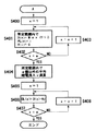
図2は、装置の製造過程における暗電流補正データの測定と記憶処理を示すフローチャートである。また、図3は、この実施形態の暗電流補正装置をカメラに応用した場合の暗電流補正処理を示すフローチャートである。
この実施形態では、100個の光電変換画素(光電変換素子)が一次元状に配列されたイメージセンサーを例に上げて説明する。そして、光電変換画素列の内の暗電流の大きい方からα個の画素を抽出し、暗電流の補正を行う。
【0010】
図4は画素ごとの暗電流を示す。
ここで、(a)に示すように、(i+1)番目の画素の暗電流が、i番目や(i+2)番目などの周辺画素の暗電流に対して大きい場合を考える。暗電流が大きい(i+1)番目の画素に対して、単純にその暗電流分を補正すると、(b)に示すように、(i+1)番目の画素の暗電流だけがほぼ0になり、周辺画素の暗電流との差が大きくなる。この状態は、あたかも(i+1)番目の画素の部分で被写体のコントラストが大きいかのように誤認されてしまい、焦点検出精度を低下させるおそれがある。
そこで、この実施形態では、(c)に示すように、暗電流が大きな(i+1)番目の画素に対して、その暗電流を周辺画素の平均的な暗電流レベル(図中に破線で示す)まで補正する。このようにすれば、暗電流補正後の全画素の暗電流レベルが平均化され、高い焦点検出精度を維持できる。
【0011】
まず、図2により装置の製造過程における暗電流補正データの測定と記憶処理を説明する。
暗電流補正データの測定と記憶処理に先だって、暗黒、常温の環境下にカメラを設置する。ステップ100において、イメージセンサー3の蓄積時間およびゲインなどのパラメータを、暗電流データ測定用の所定値に設定する。この時、画素間の暗電流差がある程度はっきりと現れるようにするために、蓄積時間を長く、ゲインを高くするとよい。ステップ101で、暗電流データ測定用のパラメータによりイメージセンサー3の電荷蓄積動作を行い、イメージセンサー3の出力をA/D変換回路4でA/D変換し、外部コンピュータへ出力する。
【0012】
外部コンピュータにおける補正値算出動作は、まずステップ102で、補正画素番号xを初期化する。次にステップ103で、100個の画素の内、暗電流が最大である画素を検出し、その暗電流値をD(x)に、画素番号をP(x)にそれぞれ記憶する。なお、i番目の画素出力をY(i)、100個の画素出力中の最大値をMax(Y(i))と表記する。また、暗電流が最大であるとして暗電流D(x)と画素番号P(x)が記憶された画素がふたたび検出されないようにするため、出力Y(i)を0に書き換える。ステップ104および105では、補正画素番号xがα個になるまでステップ103の処理を繰り返し、100個の画素の内の暗電流が大きいものから順にα個の画素の暗電流D(x)と画素番号P(x)を記憶する。
【0013】
暗電流が大きいα個の画素の暗電流データを測定したらステップ106へ進み、α個以外の画素の暗電流の平均値Avを演算する。ステップ107でふたたびxを初期化する。続くステップ108で、x番目の暗電流D(x)と平均暗電流Avとの差を取り、その差を遮光画素出力OPBで除して暗電流補正値H(x)を演算する。ステップ109および110では、補正画素番号xがα個になるまでステップ108の処理を繰り返し、100個の画素の内の暗電流が大きいものから順にα個の画素の暗電流補正値H(x)を演算する。ステップ111で、α個の画素の暗電流補正値H(x)、画素番号P(x)および補正データ測定時の温度Tを補正データ記憶部6に記憶する。
【0014】
ここで、ステップ101における電荷蓄積動作はランダムノイズの影響を避けるために複数回行い、その平均データを取得してステップ102以降の処理を行うようにしてもよい。
【0015】
次に、温度補正データを求める。
温度tを変えながら例えば画素番号1の画素の暗電流D(1)を測定すると、図6に示すような暗電流の温度特性が得られる。この温度特性の関数を求めて温度補正データf(t)とする。記憶容量が大きくなったり、演算時間が長くなるのを避けるために、温度補正データf(t)を二次関数や一次関数に近似してもよい。この温度補正データf(t)を補正データ記憶部6に記憶する。
なお、温度補正データf(t)は、1個のイメージセンサーに含まれるα個の画素の暗電流D(1)〜D(α)の温度特性を測定して平均をとったり、数個の画素の暗電流の温度特性を測定して平均をとってもよい。いずれにしても個々のイメージセンサーに対して求める必要はない。
【0016】
図3により、この実施形態の暗電流補正装置をカメラに応用した場合の暗電流補正処理を説明をする。
ステップ200において、イメージセンサー3の電荷蓄積動作を行い、その出力をA/D変換回路4でA/D変換し、暗電流補正回路5へ出力する。暗電流補正回路5では、まずステップ201で補正画素番号xを初期化する。続くステップ202で、補正データ記憶部6から暗電流補正値H(x)、補正画素番号P(x)、補正データ測定時の温度Tおよび温度補正データf(t)を読み出すとともに、温度モニター部10から使用時の温度tを入力し、これらのデータと使用時の遮光画素出力OPBとに基づいて使用環境下における暗電流補正値DK(x)を算出する。ここで、補正データ測定時の温度T℃の時に温度補正係数が1になるためには、温度補正係数はf(t)/f(T)になる。ステップ203で、出力Y(P(x))から暗電流補正値DK(x)を差し引いて補正処理を行ない、暗電流補正画素出力YH(P(x))を求める。ステップ204と205で、画素番号xがα個になるまでステップ202と203の処理を繰り返し行ない、α個の画素の暗電流補正処理を行なう。
【0017】
−発明の第2の実施の形態−
焦点検出に際しては、イメージセンサー上の全光電変換画素の出力を用いず、一部の光電変換画素の出力に基づいて焦点検出を行なう場合がある。対物レンズ、焦点検出光学系およびイメージセンサーの相対的な配置によっては、イメージセンサーの端にある光電変換画素には光束が届かない場合があり、そのような光束の届かない画素に対しては暗電流が大きくても補正の必要はない。
また、1個のイメージセンサーの中で焦点検出を行なう領域を切り換えて使用する場合に、狭い焦点検出領域に含まれる光電変換画素は使用頻度が高い。例えば、図5(a)に示すように撮影画面内に狭い焦点検出領域Nと広い焦点検出領域Wを設定した場合に、狭い焦点検出領域Nは図5(b)に示すイメージセンサー上の狭い領域N’に対応し、広い焦点検出領域Wは図5(b)に示すイメージセンサー上の広い領域W’に対応する。この場合、イメージセンサー上の狭い領域N’に含まれる光電変換画素は、焦点検出領域が狭い場合でも広い場合でも焦点検出に用いられることになる。
このような場合に、使用頻度の高い光電変換画素から優先的に暗電流補正を行うようにした第2の実施形態を説明する。なお、この第2の実施形態の構成は図1に示す第1の実施形態の構成と同様であり、説明を省略する。
【0018】
図7〜図9は、装置の製造過程における暗電流補正データの測定と記憶処理を示すフローチャートである。
概要を説明すると、まずステップ300〜304で、イメージセンサー3上の狭い領域N’において、第1の実施形態と同様に暗電流D(x)と画素番号P(x)を求める。続くステップ305〜307で、イメージセンサー3上の狭い領域N’を除く広い領域W’において、暗電流D(x)と画素番号P(x)を求める。次にステップ308〜311で、狭い領域N’において暗電流D(x)が所定値β以上である画素に対する暗電流補正値H(x)を求める。この時、暗電流補正値D(x)がβ以上である補正対象の画素が所定のα個に満たない場合には、ステップ313〜314でα個に満たない不足分を狭い領域N’を除く広い領域W’の中から求める。
【0019】
図7〜図9を参照しながら詳しく説明する。
ステップ300、301において、図2に示す第1の実施形態と同様に電荷蓄積動作を行い、暗電流データを得る。ステップ302でイメージセンサー3上の狭い領域N’を所定範囲に設定し、続くステップ303で図8に示すサブルーチンAを実行する。
【0020】
図8のサブルーチンAでは、ステップ400〜403において、所定範囲N’に含まれる画素に対して第1の実施形態と同様に出力の大きい順にα個の暗電流D(x)と画素番号PL(x)を求める。ステップ404で所定範囲N’内の残りの画素についての平均暗電流Avを求め、ステップ405〜408でα個の暗電流D(x)と平均暗電流Avとの差分DL(x)を求める。
【0021】
図7のステップ304へ戻り、差分DL(x)と画素番号PL(x)をそれぞれDN(x)とPN(x)に退避する。次に、ステップ305〜307で、(W’−N’)を所定範囲に設定し、同様に差分DL(x)と画素番号PL(x)を得てそれぞれDW(x)とPW(X)に退避させる。ステップ308でα個の補正値H(x)と画素番号P(x)を0にリセットし、続くステップ309で補正対象画素のカウント数jを0にした後、ステップ310で先に退避させたDN(x)とPN(x)の値をふたたびDL(x)とPL(x)に戻す。そして、ステップ311で図9に示すサブルーチンBを実行する。
【0022】
図9のサブルーチンBにおいて、まずステップ500で補正画素番号xを初期化する。ステップ501で、周辺画素に対して突出した差分DL(x)が所定値βより大きい場合は、この画素は補正の対象になるとしてステップ502でjをインクリメントした後、ステップ503で暗電流補正値H(x)と画素番号P(x)を求める。なお、差分DL(x)が所定値β以下の場合はステップ502と503の処理を行わない。α個の差分DL(x)に対してステップ501の判定を行ってから、図7へ戻る。
【0023】
サブルーチンBで補正の対象であると判定された画素がα個に満たない場合は、j<αとなるので図7のステップ313〜314へ進み、今度は(W’−N’)の範囲で補正対象画素の判定を行う。退避させてあるDW(x)とPW(x)の値をそれぞれ差分DL(x)と画素番号PL(x)に戻してから、ふたたびサブルーチンBを実行し、上述した判定を行う。α個の差分DL(x)全てを判定する前に、補正対象の画素がα個に達すればj=αとなり、ステップ505から図7へ戻る。また、α個の差分DL(x)全てを判定すればx=αとなり、補正対象の画素がα個に達しなくてもステップ504から図7へ戻る。こうしてα個またはそれ以下の補正値H(x)と画素番号P(x)をN’の範囲から優先的に得ることができ、ステップ315で補正データ測定時の温度Tとともに補正データ記憶部6に記憶する。
【0024】
このように、イメージセンサー中の画素範囲や焦点検出領域に優先度を設定し、優先度が高く周辺画素よりも暗電流が突出した画素から順に補正することにより、光電変換器の端にある光束が届かない画素に対する不要な暗電流補正が避けられ、限られた記憶容量で適切な補正処理がなされる。
【0025】
なお、上述した実施形態では、補正対象画素がα個に満たない場合でも、差分DL(x)が所定値β以下であるような画素に対しては補正を行わないようにしたが、この方法に限定されるものではない。α個に満たない分は、所定値βを前回よりも小さく設定して再びステップ302へ戻り、補正対象画素がα個に達するまで補正データの測定動作を繰り返してもよい。
また、複数の焦点検出エリアを有する場合、各々のエリアの使用頻度などによって補正対象画素数αをエリアごとに変えるようにしてもよい。
【0026】
【発明の効果】
(1) 請求項1の発明によれば、暗電流測定時において、複数の画素から成る光電変換器の特定の画素の暗電流とそれら特定の画素以外の画素の平均暗電流との差分を遮光画素の出力で除した値を暗電流測定時の暗電流補正値として予め記憶しておき、使用時において、遮光画素の出力と暗電流測定時の暗電流補正値とに基づいて使用時の暗電流補正値を求め、光電変換器の特定の画素の出力電流から上記使用時の暗電流補正値を減算して暗電流を補正するようにしたので、暗電流補正データを記憶するためのメモリの記憶容量を低減でき、補正処理時間を短縮できる。また、暗電流が大きな特定の画素の暗電流を周辺画素の平均的な暗電流レベルまで低減するので、暗電流補正後の全画素の暗電流レベルが平均化され、この暗電流補正装置を焦点検出装置の光電変換器に用いれば焦点検出における精度と信頼性を向上させることができる。さらに、従来のように暗電流モニター用の遮光画素出力により暗電流補正を行なわないので、いかなる温度でも最適な補正を行なうことができる。
(2) 請求項2の発明によれば、暗電流測定時の温度情報を記憶しておき、暗電流測定時の温度情報と使用時の温度情報とに基づいて上記使用時の暗電流補正値の温度補正を行ない、光電変換器の上記特定の画素の出力電流から温度補正後の使用時の暗電流補正値を減算して暗電流を補正するようにしたので、請求項1の効果に加え、温度変化による暗電流の変動を除去することができる。
(3) 請求項3の発明によれば、光電変換器の使用頻度の高い領域に含まれる画素に対して優先的に暗電流の補正を行なうようにしたので、光電変換器の端にある光束が届かない画素に対する不要な暗電流補正が避けられ、適切な補正処理がなされる。
(4) 請求項4の発明によれば、光電変換器の複数の画素の内の暗電流が大きいものから順に所定個数だけ抽出し、暗電流補正を行なう特定の画素としたので、暗電流の補正精度を向上させることができる。
【0027】
【発明の効果】
(1) 請求項1の発明によれば、複数の画素から成る光電変換器の特定の画素の暗電流とそれら特定の画素以外の画素の平均暗電流との差分を記憶しておき、光電変換器の特定の画素の出力電流から上記差分を減算して暗電流を補正するようにしたので、暗電流補正データを記憶するためのメモリの記憶容量を低減でき、補正処理時間を短縮できる。また、暗電流が大きな特定の画素の暗電流を周辺画素の平均的な暗電流レベルまで低減するので、暗電流補正後の全画素の暗電流レベルが平均化され、この暗電流補正装置を焦点検出装置の光電変換器に用いれば焦点検出における精度と信頼性を向上させることができる。さらに、従来のように暗電流モニター用の遮光画素出力により暗電流補正を行なわないので、いかなる温度でも最適な補正を行なうことができる。
(2) 請求項2の発明によれば、複数の画素から成る光電変換器の特定の画素の暗電流とそれら特定の画素以外の画素の平均暗電流との差分と、暗電流測定時の温度情報とを記憶しておき、暗電流測定時の温度情報と暗電流補正時の温度情報とに基づいて上記差分の温度補正を行ない、光電変換器の上記特定の画素の出力電流から温度補正後の差分を減算して暗電流を補正するようにしたので、請求項1の効果に加え、温度変化による暗電流の変動を除去することができる。
(3) 請求項3の発明によれば、光電変換器の使用頻度の高い領域に含まれる画素に対して優先的に暗電流の補正を行なうようにしたので、光電変換器の端にある光束が届かない画素に対する不要な暗電流補正が避けられ、適切な補正処理がなされる。
(4) 請求項4の発明によれば、光電変換器の複数の画素の内の暗電流が大きいものから順に所定個数だけ抽出し、暗電流補正を行なう特定の画素としたので、暗電流の補正精度を向上させることができる。
【図面の簡単な説明】
【図1】 第1の実施形態の構成を示す図。
【図2】 第1の実施形態の補正データの測定と記憶処理を示すフローチャート。
【図3】 カメラに応用した光電変換器の暗電流補正装置の暗電流補正処理を示すフローチャート。
【図4】 補正前後の暗電流を示す図。
【図5】 狭い焦点検出領域と広い焦点検出領域を示す図。
【図6】 温度による暗電流変化を示す図。
【図7】 第2の実施例の補正データの測定と記憶処理を示すフローチャート。
【図8】 図7に続く、第2の実施例の補正データの測定と記憶処理を示すフローチャート。
【図9】 図8に続く、第2の実施例の補正データの測定と記憶処理を示すフローチャート。
【符号の説明】
1 対物レンズ
2 焦点検出光学系
3 イメージセンサー
4 A/D変換回路
5 暗電流補正回路
6 補正データ記憶部
7 演算部
8 駆動制御部
9 モーター[0001]
BACKGROUND OF THE INVENTION
The present invention relates to an apparatus for correcting dark current included in an output of a photoelectric converter.
[0002]
[Prior art]
An image sensor is used for a focus detection device such as a camera. This image sensor has a plurality of charge storage photoelectric conversion pixels arranged one-dimensionally. The output of the image sensor reflects the light luminance distribution of the subject, and the focus detection device detects the focus adjustment state of the photographing lens based on the output of the image sensor.
[0003]
By the way, when the subject has low luminance, the accumulation time is lengthened in order to obtain an image sensor output of a predetermined level or more, but this also increases the dark current and lowers the S / N ratio. The magnitude of the dark current varies from one photoelectric conversion pixel to another, and if the dark current of a certain pixel is significantly larger than the dark current of the surrounding pixels, it looks as if the subject has high contrast. (See FIG. 4A). In particular, when the luminance is low, the output level of all the photoelectric conversion pixels is low, the dark current component is relatively large, and the focus detection performance is greatly adversely affected. Further, since the magnitude of the dark current depends not only on the accumulation time but also on the temperature, the dark current increases and the S / N ratio decreases at high temperatures.
[0004]
In order to solve such a problem, a method of correcting a dark current included in the output of an image sensor has been proposed. For example, Japanese Patent Laid-Open No. 3-10473 discloses an image sensor provided with a light-shielding pixel portion for monitoring a dark current in addition to an aperture pixel portion. By calculating the dark current increase / decrease rate from the ratio of the shaded pixel output during the focus detection operation and the stored shaded pixel output, and multiplying the stored aperture pixel output by the ratio, The dark current for each pixel is obtained. Here, the aperture pixel is a pixel on the image sensor to which a light beam from a subject is irradiated by the focus detection optical system.
[0005]
[Problems to be solved by the invention]
However, the conventional dark current correction device for a photoelectric converter needs to store dark current of all pixels, and has a large capacity when many photoelectric converters are used like a multipoint ranging type focus detection device. Memory is required, and the correction time becomes long.
Further, the dark pixel output for dark current monitoring may not necessarily reflect the temperature depending on the configuration of the image sensor. For example, when the environmental temperature of the image sensor is about 50 ° C. or less due to the influence of the heat of the peripheral circuit, the light-shielded pixel output becomes substantially constant with respect to the temperature. For this reason, there is also a problem that optimum correction cannot be performed for the output of the aperture pixel including the dark current component depending on the temperature.
[0006]
An object of the present invention is to provide a dark current correction device for a photoelectric converter that does not require a large-capacity memory and corrects the dark current accurately in a short time.
[0007]
[Means for Solving the Problems]
(1) According to the first aspect of the present invention, at the time of dark current measurement , the difference between the dark current of a specific pixel of a photoelectric converter composed of a plurality of pixels and the average dark current of pixels other than the specific pixel is determined by the shading pixel. The value divided by the output is stored in advance as a dark current correction value during dark current measurement, and during use, the dark current correction during use is based on the output of the light-shielded pixels and the dark current correction value during dark current measurement. The value is obtained, and the dark current correction value is subtracted from the output current of a specific pixel of the photoelectric converter to correct the dark current.
(2) dark current correction apparatus of the photoelectric converter according to
(3) The dark current correction device for a photoelectric converter according to
(4) The dark current correction device for a photoelectric converter according to
[0008]
DETAILED DESCRIPTION OF THE INVENTION
-First embodiment of the invention-
FIG. 1 shows the configuration of the first embodiment of the present invention.
The light beam from the subject that has passed through the
The dark current correction circuit 5 corrects the dark current included in the subject image signal of the
[0009]
FIG. 2 is a flowchart showing dark current correction data measurement and storage processing in the manufacturing process of the apparatus. FIG. 3 is a flowchart showing dark current correction processing when the dark current correction apparatus of this embodiment is applied to a camera.
In this embodiment, an image sensor in which 100 photoelectric conversion pixels (photoelectric conversion elements) are arranged one-dimensionally will be described as an example. Then, α pixels are extracted from the photoelectric conversion pixel array having the larger dark current, and the dark current is corrected.
[0010]
FIG. 4 shows the dark current for each pixel.
Here, as shown in (a), a case is considered where the dark current of the (i + 1) th pixel is larger than the dark current of peripheral pixels such as the i-th and (i + 2) -th pixels. If the dark current is simply corrected for the (i + 1) -th pixel having a large dark current, only the dark current of the (i + 1) -th pixel becomes almost zero as shown in FIG. The difference from the dark current increases. This state may be mistaken as if the contrast of the subject is large at the (i + 1) th pixel portion, which may reduce the focus detection accuracy.
Therefore, in this embodiment, as shown in (c), for the (i + 1) th pixel having a large dark current, the dark current is an average dark current level of peripheral pixels (indicated by a broken line in the figure). Correct until. In this way, the dark current levels of all pixels after dark current correction are averaged, and high focus detection accuracy can be maintained.
[0011]
First, the measurement and storage processing of dark current correction data in the manufacturing process of the apparatus will be described with reference to FIG.
Prior to measuring and storing dark current correction data, the camera is installed in a dark, room temperature environment. In
[0012]
In the correction value calculation operation in the external computer, first, in
[0013]
When the dark current data of α pixels having a large dark current is measured, the process proceeds to step 106, and an average value Av of dark currents of pixels other than α is calculated. In
[0014]
Here, the charge accumulation operation in step 101 may be performed a plurality of times in order to avoid the influence of random noise, and the average data may be acquired to perform the processing after
[0015]
Next, temperature correction data is obtained.
For example, when the dark current D (1) of the pixel of
Note that the temperature correction data f (t) is obtained by measuring the temperature characteristics of the dark currents D (1) to D (α) of α pixels included in one image sensor and taking an average, or several pixels. The temperature characteristics of the dark current may be measured and averaged. In any case, it is not necessary to obtain for each image sensor.
[0016]
The dark current correction process when the dark current correction apparatus of this embodiment is applied to a camera will be described with reference to FIG.
In
[0017]
-Second embodiment of the invention-
In focus detection, focus detection may be performed based on the output of some photoelectric conversion pixels without using the output of all photoelectric conversion pixels on the image sensor. Depending on the relative arrangement of the objective lens, focus detection optical system, and image sensor, the light beam may not reach the photoelectric conversion pixels at the edge of the image sensor. No correction is necessary even if the current is large.
In addition, when a focus detection region is switched and used in one image sensor, photoelectric conversion pixels included in a narrow focus detection region are frequently used. For example, when a narrow focus detection area N and a wide focus detection area W are set in the shooting screen as shown in FIG. 5A, the narrow focus detection area N is narrow on the image sensor shown in FIG. A wide focus detection area W corresponding to the area N ′ corresponds to a wide area W ′ on the image sensor shown in FIG. In this case, the photoelectric conversion pixels included in the narrow area N ′ on the image sensor are used for focus detection regardless of whether the focus detection area is narrow or wide.
In such a case, a second embodiment will be described in which dark current correction is performed preferentially from photoelectric conversion pixels that are frequently used. The configuration of the second embodiment is the same as that of the first embodiment shown in FIG.
[0018]
7 to 9 are flowcharts showing dark current correction data measurement and storage processing in the manufacturing process of the apparatus.
The outline will be described. First, in
[0019]
This will be described in detail with reference to FIGS.
In
[0020]
In the subroutine A of FIG. 8, in
[0021]
Returning to step 304 in FIG. 7, the difference DL (x) and the pixel number PL (x) are saved to DN (x) and PN (x), respectively. Next, in steps 305 to 307, (W′−N ′) is set to a predetermined range, and similarly, a difference DL (x) and a pixel number PL (x) are obtained, and DW (x) and PW (X), respectively. Evacuate. In
[0022]
In subroutine B of FIG. 9, first, at
[0023]
If the number of pixels determined to be corrected in subroutine B is less than α, j <α, so the process proceeds to
[0024]
In this way, by setting priority to the pixel range and focus detection area in the image sensor, and correcting in order from the pixel with higher priority and the dark current protruding from the surrounding pixels, the light flux at the end of the photoelectric converter Unnecessary dark current correction for pixels that do not reach is avoided, and appropriate correction processing is performed with a limited storage capacity.
[0025]
In the above-described embodiment, correction is not performed for pixels whose difference DL (x) is equal to or less than the predetermined value β even when the number of correction target pixels is less than α. It is not limited to. If less than α, the predetermined value β may be set smaller than the previous time, and the process may return to step 302 again, and the correction data measurement operation may be repeated until the number of correction target pixels reaches α.
When a plurality of focus detection areas are provided, the correction target pixel number α may be changed for each area depending on the frequency of use of each area.
[0026]
【The invention's effect】
(1) According to the first aspect of the invention, during dark current measurement, the difference between the dark current of a specific pixel of a photoelectric converter composed of a plurality of pixels and the average dark current of pixels other than the specific pixel is shielded. The value divided by the pixel output is stored in advance as a dark current correction value at the time of dark current measurement, and at the time of use, based on the output of the light-shielded pixel and the dark current correction value at the time of dark current measurement, Since the current correction value is obtained and the dark current correction value is subtracted from the output current of a specific pixel of the photoelectric converter to correct the dark current, the memory for storing the dark current correction data is stored. The storage capacity can be reduced and the correction processing time can be shortened. In addition, since the dark current of a specific pixel having a large dark current is reduced to the average dark current level of surrounding pixels, the dark current level of all pixels after dark current correction is averaged, and this dark current correction device is focused. If used in the photoelectric converter of the detection device, the accuracy and reliability in focus detection can be improved. Further, since the dark current correction is not performed by the dark pixel output for monitoring the dark current as in the prior art, the optimum correction can be performed at any temperature.
(2) According to the invention of
(3) According to the invention of
(4) According to the invention of
[0027]
【The invention's effect】
(1) According to the invention of
(2) According to the invention of
(3) According to the invention of
(4) According to the invention of
[Brief description of the drawings]
FIG. 1 is a diagram showing a configuration of a first embodiment.
FIG. 2 is a flowchart showing correction data measurement and storage processing according to the first embodiment;
FIG. 3 is a flowchart showing dark current correction processing of a dark current correction device for a photoelectric converter applied to a camera.
FIG. 4 is a diagram showing dark current before and after correction.
FIG. 5 is a diagram showing a narrow focus detection area and a wide focus detection area.
FIG. 6 is a diagram showing changes in dark current due to temperature.
FIG. 7 is a flowchart showing correction data measurement and storage processing according to the second embodiment;
FIG. 8 is a flowchart illustrating correction data measurement and storage processing according to the second embodiment, following FIG. 7;
FIG. 9 is a flowchart showing correction data measurement and storage processing of the second embodiment, following FIG. 8;
[Explanation of symbols]
DESCRIPTION OF
Claims (4)
使用時において、前記遮光画素の出力と前記暗電流測定時の暗電流補正値とに基づいて使用時の暗電流補正値を求め、前記光電変換器の前記特定の画素の出力電流から前記使用時の暗電流補正値を減算して暗電流を補正する補正手段とを備えることを特徴とする光電変換器の暗電流補正装置。 During dark current measurement, a value obtained by dividing the difference between the dark current of a specific pixel of a photoelectric converter composed of a plurality of pixels and the average dark current of pixels other than the specific pixel by the output of the light-shielded pixel is measured. Storage means for storing in advance as a dark current correction value of
In use, the calculated dark current correction value at the time of use on the basis of the output of light-shielded pixel and the dark current correction value when the dark current measurement, when the use of the output current of the particular pixel of said photoelectric converter And a correction means for correcting the dark current by subtracting the dark current correction value .
前記記憶手段は暗電流測定時の温度情報を記憶し、
前記補正手段は、前記記憶手段に記憶されている暗電流測定時の温度情報と、使用時の温度情報とに基づいて前記使用時の暗電流補正値の温度補正を行ない、前記光電変換器の前記特定の画素の出力電流から前記温度補正後の使用時の暗電流補正値を減算して暗電流を補正することを特徴とする光電変換器の暗電流補正装置。In the dark current correction device for a photoelectric converter according to claim 1,
The storage means stores temperature information at the time of dark current measurement,
The correction means performs temperature correction of the dark current correction value at the time of use based on temperature information at the time of dark current measurement stored in the storage means and temperature information at the time of use, and the photoelectric converter A dark current correction device for a photoelectric converter, wherein a dark current is corrected by subtracting a dark current correction value in use after temperature correction from an output current of the specific pixel.
前記補正手段は、前記光電変換器の使用頻度の高い領域に含まれる画素に対して優先的に暗電流の補正を行なうことを特徴とする光電変換器の暗電流補正装置。In the dark current correction device for a photoelectric converter according to claim 1 or 2,
The dark current correction device for a photoelectric converter, wherein the correction means preferentially corrects dark current for pixels included in a region where the photoelectric converter is frequently used.
前記特定の画素は、前記光電変換器の複数の画素の内の暗電流が大きいものから順に所定個数だけ抽出した画素であることを特徴とする光電変換器の暗電流補正装置。In the dark current correction device for a photoelectric converter according to any one of claims 1 to 3,
The specific current pixel is a dark current correction device for a photoelectric converter, wherein a predetermined number of pixels are extracted in descending order of the dark current among the plurality of pixels of the photoelectric converter.
Priority Applications (1)
| Application Number | Priority Date | Filing Date | Title |
|---|---|---|---|
| JP16418496A JP3806973B2 (en) | 1996-06-25 | 1996-06-25 | Dark current correction device for photoelectric converter |
Applications Claiming Priority (1)
| Application Number | Priority Date | Filing Date | Title |
|---|---|---|---|
| JP16418496A JP3806973B2 (en) | 1996-06-25 | 1996-06-25 | Dark current correction device for photoelectric converter |
Publications (2)
| Publication Number | Publication Date |
|---|---|
| JPH1013749A JPH1013749A (en) | 1998-01-16 |
| JP3806973B2 true JP3806973B2 (en) | 2006-08-09 |
Family
ID=15788304
Family Applications (1)
| Application Number | Title | Priority Date | Filing Date |
|---|---|---|---|
| JP16418496A Expired - Lifetime JP3806973B2 (en) | 1996-06-25 | 1996-06-25 | Dark current correction device for photoelectric converter |
Country Status (1)
| Country | Link |
|---|---|
| JP (1) | JP3806973B2 (en) |
Cited By (1)
| Publication number | Priority date | Publication date | Assignee | Title |
|---|---|---|---|---|
| WO2010125609A1 (en) * | 2009-04-30 | 2010-11-04 | 株式会社島津製作所 | Light or radiation imaging device |
Families Citing this family (8)
| Publication number | Priority date | Publication date | Assignee | Title |
|---|---|---|---|---|
| FR2803082B1 (en) * | 1999-12-28 | 2002-03-22 | Trixell Sas | METHOD FOR TEMPERATURE COMPENSATION OF THE SENSITIVITY OF AN IMAGE DETECTOR |
| JP2003015022A (en) * | 2001-06-29 | 2003-01-15 | Canon Inc | Range-finding device, range-finding method and control program |
| US7372484B2 (en) * | 2003-06-26 | 2008-05-13 | Micron Technology, Inc. | Method and apparatus for reducing effects of dark current and defective pixels in an imaging device |
| JP4534715B2 (en) * | 2004-10-22 | 2010-09-01 | 株式会社ニコン | Imaging apparatus and image processing program |
| JP4789245B2 (en) * | 2006-01-13 | 2011-10-12 | 株式会社日立メディコ | X-ray diagnostic imaging equipment |
| WO2010109539A1 (en) * | 2009-03-27 | 2010-09-30 | 株式会社島津製作所 | Image pickup apparatus |
| JP5413280B2 (en) * | 2010-04-05 | 2014-02-12 | 株式会社島津製作所 | Imaging device |
| WO2015072006A1 (en) * | 2013-11-15 | 2015-05-21 | 富士通株式会社 | Infrared ray detection device |
-
1996
- 1996-06-25 JP JP16418496A patent/JP3806973B2/en not_active Expired - Lifetime
Cited By (1)
| Publication number | Priority date | Publication date | Assignee | Title |
|---|---|---|---|---|
| WO2010125609A1 (en) * | 2009-04-30 | 2010-11-04 | 株式会社島津製作所 | Light or radiation imaging device |
Also Published As
| Publication number | Publication date |
|---|---|
| JPH1013749A (en) | 1998-01-16 |
Similar Documents
| Publication | Publication Date | Title |
|---|---|---|
| US7474352B2 (en) | Focus detection based on an opening pupil ratio | |
| US7796176B2 (en) | Phase adjusting device, phase adjusting method, and digital camera | |
| US7995133B2 (en) | Method, apparatus for correcting image signal from image sensor, and imaging system with apparatus | |
| US9838625B2 (en) | Image processing apparatus and control method for image processing apparatus for controlling correction of a black level in a combined image signal | |
| US7907194B2 (en) | Imaging apparatus and gain adjusting method for the same | |
| US11363219B2 (en) | Information processing apparatus, image sensor, image capturing apparatus, and information processing method | |
| CN104333680A (en) | Image capturing apparatus and image processing method | |
| US6973262B2 (en) | Camera and wide-angle field distance-measuring camera | |
| JP3806973B2 (en) | Dark current correction device for photoelectric converter | |
| US11159740B2 (en) | Image capturing device and control method thereof and medium | |
| US9961255B2 (en) | Image capturing apparatus, control method thereof, and storage medium | |
| KR20060063724A (en) | Imaging apparatus, imaging method and imaging processing program | |
| JP6334976B2 (en) | Digital camera with focus detection pixels used for photometry | |
| JP5701942B2 (en) | Imaging apparatus, camera system, and image processing method | |
| US8436923B2 (en) | Imaging apparatus having a function for estimating a dark current amount | |
| US7801429B2 (en) | Image taking apparatus | |
| JP2021063976A (en) | Focus detector and method for controlling the same, program, and storage medium | |
| CN101616254B (en) | Image processing apparatus and image processing method | |
| JP6118133B2 (en) | Signal processing apparatus and imaging apparatus | |
| JP4662343B2 (en) | Imaging apparatus and correction method | |
| US11917300B2 (en) | Image pickup apparatus and image pickup element, which are capable of performing appropriate correction processing that suppresses influence of high luminance light, control method for image pickup apparatus, and storage medium | |
| JP3955144B2 (en) | Ranging device | |
| JP4321317B2 (en) | Electronic camera, camera system, and black spot correction method for electronic camera | |
| JP2008028634A (en) | Imaging apparatus | |
| JP6590585B2 (en) | Imaging apparatus and exposure control method |
Legal Events
| Date | Code | Title | Description |
|---|---|---|---|
| A977 | Report on retrieval |
Free format text: JAPANESE INTERMEDIATE CODE: A971007 Effective date: 20060419 |
|
| TRDD | Decision of grant or rejection written | ||
| A01 | Written decision to grant a patent or to grant a registration (utility model) |
Free format text: JAPANESE INTERMEDIATE CODE: A01 Effective date: 20060425 |
|
| A61 | First payment of annual fees (during grant procedure) |
Free format text: JAPANESE INTERMEDIATE CODE: A61 Effective date: 20060508 |
|
| R150 | Certificate of patent or registration of utility model |
Free format text: JAPANESE INTERMEDIATE CODE: R150 |
|
| FPAY | Renewal fee payment (event date is renewal date of database) |
Free format text: PAYMENT UNTIL: 20120526 Year of fee payment: 6 |
|
| FPAY | Renewal fee payment (event date is renewal date of database) |
Free format text: PAYMENT UNTIL: 20150526 Year of fee payment: 9 |
|
| S531 | Written request for registration of change of domicile |
Free format text: JAPANESE INTERMEDIATE CODE: R313531 |
|
| FPAY | Renewal fee payment (event date is renewal date of database) |
Free format text: PAYMENT UNTIL: 20150526 Year of fee payment: 9 |
|
| R350 | Written notification of registration of transfer |
Free format text: JAPANESE INTERMEDIATE CODE: R350 |
|
| FPAY | Renewal fee payment (event date is renewal date of database) |
Free format text: PAYMENT UNTIL: 20150526 Year of fee payment: 9 |
|
| R250 | Receipt of annual fees |
Free format text: JAPANESE INTERMEDIATE CODE: R250 |
|
| R250 | Receipt of annual fees |
Free format text: JAPANESE INTERMEDIATE CODE: R250 |
|
| EXPY | Cancellation because of completion of term |