JP3803000B2 - Method for monitoring optical power deviation between wavelengths, and optical equalizer and optical amplifier using the same - Google Patents
Method for monitoring optical power deviation between wavelengths, and optical equalizer and optical amplifier using the same Download PDFInfo
- Publication number
- JP3803000B2 JP3803000B2 JP27501199A JP27501199A JP3803000B2 JP 3803000 B2 JP3803000 B2 JP 3803000B2 JP 27501199 A JP27501199 A JP 27501199A JP 27501199 A JP27501199 A JP 27501199A JP 3803000 B2 JP3803000 B2 JP 3803000B2
- Authority
- JP
- Japan
- Prior art keywords
- optical
- light
- wavelength
- measurement
- channel
- Prior art date
- Legal status (The legal status is an assumption and is not a legal conclusion. Google has not performed a legal analysis and makes no representation as to the accuracy of the status listed.)
- Expired - Fee Related
Links
Images


Classifications
-
- H—ELECTRICITY
- H04—ELECTRIC COMMUNICATION TECHNIQUE
- H04J—MULTIPLEX COMMUNICATION
- H04J14/00—Optical multiplex systems
- H04J14/02—Wavelength-division multiplex systems
- H04J14/0221—Power control, e.g. to keep the total optical power constant
-
- H—ELECTRICITY
- H04—ELECTRIC COMMUNICATION TECHNIQUE
- H04B—TRANSMISSION
- H04B10/00—Transmission systems employing electromagnetic waves other than radio-waves, e.g. infrared, visible or ultraviolet light, or employing corpuscular radiation, e.g. quantum communication
- H04B10/25—Arrangements specific to fibre transmission
- H04B10/2507—Arrangements specific to fibre transmission for the reduction or elimination of distortion or dispersion
- H04B10/25073—Arrangements specific to fibre transmission for the reduction or elimination of distortion or dispersion using spectral equalisation, e.g. spectral filtering
-
- H—ELECTRICITY
- H04—ELECTRIC COMMUNICATION TECHNIQUE
- H04J—MULTIPLEX COMMUNICATION
- H04J14/00—Optical multiplex systems
- H04J14/02—Wavelength-division multiplex systems
- H04J14/0201—Add-and-drop multiplexing
-
- H—ELECTRICITY
- H04—ELECTRIC COMMUNICATION TECHNIQUE
- H04J—MULTIPLEX COMMUNICATION
- H04J14/00—Optical multiplex systems
- H04J14/02—Wavelength-division multiplex systems
- H04J14/0201—Add-and-drop multiplexing
- H04J14/0202—Arrangements therefor
- H04J14/0208—Interleaved arrangements
-
- H—ELECTRICITY
- H04—ELECTRIC COMMUNICATION TECHNIQUE
- H04J—MULTIPLEX COMMUNICATION
- H04J14/00—Optical multiplex systems
- H04J14/02—Wavelength-division multiplex systems
- H04J14/0201—Add-and-drop multiplexing
- H04J14/0202—Arrangements therefor
- H04J14/021—Reconfigurable arrangements, e.g. reconfigurable optical add/drop multiplexers [ROADM] or tunable optical add/drop multiplexers [TOADM]
-
- H—ELECTRICITY
- H04—ELECTRIC COMMUNICATION TECHNIQUE
- H04J—MULTIPLEX COMMUNICATION
- H04J14/00—Optical multiplex systems
- H04J14/02—Wavelength-division multiplex systems
- H04J14/0201—Add-and-drop multiplexing
- H04J14/0202—Arrangements therefor
- H04J14/0213—Groups of channels or wave bands arrangements
Description
【0001】
【発明の属する技術分野】
本発明は、各種の光通信において利用される波長多重(WDM)信号光の光パワーの波長特性を簡易な手法で、かつ、精度良くモニタする波長間光パワー偏差のモニタ方法、並びに、そのモニタ方法を用いてWDM信号光の光パワーの波長特性の等化処理を制御するようにした光等化器および光増幅器に関する。
【0002】
【従来の技術】
光通信において、複数の波長の光を1本の光ファイバで伝送することにより通信容量を増大する波長多重(WDM)伝送方式の研究開発が活発化している。このWDM伝送方式は、既存の光ファイバを利用できるため、導入コストが低いこと、また、広い増幅帯域を有する光増幅器を用いることで伝送路はビットレートフリーとなり将来のアップグレードが容易であるなどの利点があり、将来のマルチメディア社会を実現する手段として期待されている。
【0003】
一般に、光増幅器を用いたWDM光通信システムにおいては、所定の伝送特性を得るために、各増幅中継段において各チャネル間の光パワーの偏差(チルト)を数dB以下に抑えて伝送する必要がある。これは、伝送可能な光パワーの上限が光伝送路の非線形効果による波形劣化により制限され、下限が受信S/Nの劣化により制限されるためである。
【0004】
しかし、光ファイバ伝送路では、非線形効果のひとつである誘導ラマン散乱(stimulated Raman scattering)やレイリー散乱によって、その損失に波長特性が生じることが知られている。特に、誘導ラマン散乱による損失波長特性は、光伝送路の長さ、チャネル数(信号光の波長数)、チャネル間隔(信号光の波長間隔)、光パワーレベル等といった様々な伝送条件に応じて、その大きさが異なって発生する。一般的に、WDM光伝送システムにおけるチャネル数や使用波長は、システム利用者によって適宜に設定可能とされるため、それらの値が常時一定であるとは限らない。例えば光波ネットワーク等においては、光ADM(Optical Add and Drop Multiplexer)装置に入力される信号光の数や波長位置がダイナミックに変化するため、大きさの異なる損失波長特性が光伝送路に発生してしまい、これによって、伝送特性への影響が深刻な問題になる。
【0005】
また、各種の光通信システムを構成する光増幅器および分散補償器等についても、利得および損失に波長特性を有することが知られており、これらの利得および損失の波長特性によって、各チャネル間の光パワーに偏差が生じて伝送特性に大きな影響を及ぼすことが問題になる。
【0006】
そこで、WDM光通信システムで生じる各チャネル間の光パワーの偏差をモニタ(監視)して、この偏差を低減する対策を施すことが要求される。これに対して本発明者は、例えば、WDM光通信システムに能動的な利得等化器を適用し、各チャネル間の光パワーの偏差のモニタ値が小さくなるように、前記利得等化器の特性を制御する技術を提案している(特願平11−54374号、特願平11−115971号等参照)。
【0007】
上記の先願発明にも適用されている、チャネル間の光パワーの偏差をモニタする従来のモニタ方法としては、例えば、光増幅器が発生する自然放出(ASE)光を基にチャネル間の光パワーの偏差を算出する方法がある(特願平11−054374号参照)。この方法では、信号光帯域の近傍における自然放出光パワーがモニタされるため、入力する信号数やチャネルの変動に依存することなくチャネル間の光パワーのばらつきをモニタできる。また、例えば、一般的な光スペクトルアナライザ等を用いて各チャネルの光パワーを直接測定し、チャネル間の光パワーの偏差を算出する方法も知られている。
【0008】
【発明が解決しようとする課題】
しかしながら、上記従来の波長間光パワー偏差のモニタ方法のうちの自然放出光を利用したモニタ方法については、信号光自体を直接モニタするのではなく自然放出光をモニタするという間接的な方法であるため、モニタ誤差が生じる虞があった。また、光スペクトルアナライザ等を用いて各信号光パワーを直接測定するモニタ方法については、例えば、信号光帯域に最も密に信号光が入力した場合においても、各信号光パワーを正確に測定できなければならないため、優れた波長分解能を有する高性能な光スペクトルアナライザ等を使用して信号光パワーの測定を行う必要がある。したがって、このモニタ方法を適用した装置にあっては、コストの上昇およびサイズの大型化を招いてしまうという問題があった。
【0009】
本発明は上記の点に着目してなされたもので、高い波長分解能を必要とすることなく信号光パワーを直接測定して、チャネル間の光パワーの偏差を高精度に検出するモニタ方法、並びに、そのモニタ方法を適用して小型化および低価格化を図った光等化器および光増幅器を提供することを目的とする。
【0010】
【課題を解決するための手段】
上記の目的を達成するため、本発明による波長間光パワー偏差のモニタ方法は、波長の異なる複数のチャネル光が波長多重されたWDM信号光に関するチャネル情報を得る過程と、該チャネル情報に基づいて、少なくとも1つの異なるチャネル光を含んだ複数の測定波長域を設定する過程と、該各測定波長域についてのみ、WDM信号光のチャネル光パワーを測定する過程と、該光パワーの測定値を用いて各測定波長域についての光パワー比を求め、WDM信号光の波長間光パワー偏差を判断する過程と、を含んでなる方法である。
【0011】
かかるモニタ方法によれば、WDM信号光に含まれる各チャネル光の波長位置や伝送速度等に関するチャネル情報に基づいて、光パワーの測定に適した少なくとも2つの測定波長域が設定され、該各測定波長域に限ってチャネル光パワーが測定されて、その測定結果を基に各測定波長域についての光パワー比から波長間光パワー偏差が判断されるようになる。これにより、比較的低い波長分解能でも信号光パワーを直接測定しながら高い精度でWDM信号光パワーの波長特性をモニタできる。
【0012】
なお、少なくとも1つの異なるチャネル光を含んだ複数の測定波長域については、各測定波長域が1つのチャネル光をそれぞれ有し、各々のチャネル光が相互に異なる場合と、各測定波長域が複数のチャネル光をそれぞれ有し、該複数のチャネル光のうちの少なくとも1つが相互に異なる場合とが可能であり、また、それら2つの場合を組み合わせた複数の測定波長域とすることも可能である。
【0013】
上記のモニタ方法について、測定波長域を設定する過程は、入力チャネルのうちの最短波長チャネル光を含んだ第1測定波長域と、最長波長チャネル光を含んだ第2測定波長域とを少なくとも設定するようにしてもよい。また、雑音光を含む割合が最小となるように各測定波長域を設定するのが望ましい。このようにすることで、各チャネル光の光パワー偏差の測定精度を向上させることが可能になる。
【0014】
さらに、チャネル情報を得る過程は、具体的には、WDM信号光に伴なって伝達される監視信号光を基に、WDM信号光の各チャネル光の波長位置および伝送速度を含んだチャネル情報を得るようにしてもよい。
【0015】
本発明による光等化器は、波長の異なる複数のチャネル光が波長多重されたWDM信号光の光パワーの波長特性を等化する光等化器において、可変の光等化特性を有し、WDM信号光が入力される可変光等化手段と、WDM信号光についてのチャネル情報を得るチャネル情報取得手段と、該チャネル情報取得手段で得たチャネル情報に基づいて、少なくとも1つの異なるチャネル光を含んだ複数の測定波長域を設定する波長域設定手段と、波長域設定手段で設定された各測定波長域についてのみ、可変光等化手段を通過したWDM信号光のチャネル光パワーを測定する光パワー測定手段と、チャネル情報取得手段で得たチャネル情報を基に、WDM信号光の光パワー波長特性を平坦にする各測定波長域についての光パワー比の目標値を求めると共に、光パワー測定手段の測定結果を用いて各測定波長域についての光パワー比の測定値を求め、該測定値が目標値に略等しくなるように、可変光等化手段の光等化特性を制御する制御手段と、を含んで構成されるものでる。
【0016】
また、本発明による光増幅器の一態様は、波長の異なる複数のチャネル光が波長多重されたWDM信号光を一括して増幅する光増幅手段を備えた光増幅器において、可変の利得等化特性を有し、WDM信号光が入力される可変利得等化手段と、WDM信号光についてのチャネル情報を得るチャネル情報取得手段と、該チャネル情報取得手段で得たチャネル情報に基づいて、少なくとも1つの異なるチャネル光を含んだ複数の測定波長域を設定する波長域設定手段と、波長域設定手段で設定された各測定波長域についてのみ、可変利得等化手段を通過したWDM信号光のチャネル光パワーを測定する光パワー測定手段と、チャネル情報取得手段で得たチャネル情報を基に、WDM信号光の光パワー波長特性を平坦にする各測定波長域についての光パワー比の目標値を求めると共に、光パワー測定手段の測定結果を用いて各測定波長域についての光パワー比の測定値を求め、該測定値が目標値に略等しくなるように、可変利得等化手段の利得等化特性を制御する制御手段と、を含んで構成されるものである。
【0017】
かかる構成の光等化器または光増幅器では、前述した本発明によるモニタ方法がチャネル情報取得手段、波長域設定手段、光パワー測定手段および制御手段のそれぞれの動作によって実現され、そのモニタ結果に応じて可変光等化手段または可変利得等化手段の等化特性がフィードバック制御されるようになる。これにより、WDM信号光の光パワー波長特性の等化処理を確実に行うことのできる小型で安価な光等化器または光増幅器を提供することが可能になる。
【0018】
さらに、上記光等化器または光増幅器の具体的な構成として、光パワー測定手段は、可変光等化手段を通過したWDM信号光の一部が入射されて回折光を発生する回折格子と、該回折格子で回折された各チャネル光の到達位置に対応させて配置された複数の受光素子を有し、波長域設定手段で設定された各測定波長域に対応する受光素子における光パワーの測定結果を選択して制御手段に伝える受光部と、を含むようにしてもよい。加えて、前記受光部は、WDM信号光に含まれる最大チャネル数以下で、かつ、2個以上の受光素子を有することが可能である。
【0019】
かかる構成の光パワー測定手段では、回折格子による光の回折を利用して、各チャネル光パワーが対応する受光素子ごとに測定され、各々の測定波長域に対応する受光素子の測定結果が選択的に制御手段に伝えられるようになる。
【0020】
あるいは、光パワー測定手段の他の具体的な構成としては、可変光等化手段を通過したWDM信号光の一部が入力され、波長域設定手段で設定された各測定波長域に応じて、通過帯域の中心波長が時間変化する可変光フィルタと、該可変光フィルタを通過したチャネル光のパワーを測定する受光部と、該受光部における測定結果のうちで波長域設定手段で設定された各測定波長域に対応するデータを選択して制御手段に伝える選択部と、を含むようにしてもよい。
【0021】
かかる構成の光パワー測定手段では、可変光フィルタの通過帯域の時間変化に応じて、各チャネル光のパワーが受光部で測定され、可変光フィルタの通過帯域が測定波長域に対応した時の受光素子の測定結果が選択的に制御手段に伝えられるようになる。
【0022】
また、本発明による光増幅器の他の態様としては、波長の異なる複数のチャネル光が波長多重されたWDM信号光を少なくとも2つの増幅波長帯に分波する分波手段と、該分波手段で分波された各増幅波長帯の光信号をそれぞれ増幅する少なくとも2つの光増幅手段と、該各光増幅手段で増幅された各光信号を合波する合波手段とを備えた光増幅器において、可変の利得等化特性を有し、分波手段の入力側前段に設けられる可変利得等化手段と、WDM信号光についてのチャネル情報を得るチャネル情報取得手段と、各光増幅手段に入力される各増幅波長帯の光信号の一部を入力して、各光増幅手段へのトータル入力パワーをそれぞれ測定する入力パワー測定手段と、チャネル情報取得手段で得たチャネル情報を基に、WDM信号光の光パワー波長特性を平坦にする各光増幅手段についてのトータル入力パワー比の目標値を求めると共に、入力パワー測定手段の測定結果を用いて前記各光増幅手段についてのトータル入力パワー比の測定値を求め、該測定値が目標値に略等しくなるように、可変利得等化手段の利得等化特性を制御する制御手段と、を含んで構成されるものである。
【0023】
かかる構成の光増幅器では、広い信号光帯域を有するWDM信号光が可変利得等化手段を介して分波手段に送られて複数の増幅波長帯に分波される。分波された各増幅波長帯の光信号は、対応する光増幅手段でそれぞれ増幅された後に合波手段によって合波される。このとき、各光増幅手段に入力される各々の光信号の一部が入力パワー測定手段にそれぞれ送られてトータル入力パワーがモニタされ、そのモニタ結果に応じて、入力段に設けた可変利得等化手段の利得等化特性が制御手段によりフィードバック制御されるようになる。この場合、各増幅波長帯は上述のモニタ方法の各測定波長域に相当し、チャネル情報取得手段、入力パワー測定手段および制御手段のそれぞれの動作によって本発明によるモニタ方法が実現される。これにより、増幅波長帯の異なる各光増幅手段への入力光のチルトを簡易なモニタ方法を用いて確実に補償することができるようになる。この構成のポイントは2つある。第1のポイントは、光増幅手段の入力側でチルトを補償するので、伝送光パワーが劣化しているチャネルの雑音指数を救済するため、光増幅器のチルト補償だけでなく雑音指数の波長特性を抑えて、光SNRにも有利に働くことである。第2のポイントは、通常の光増幅器には、入力パワーをモニタする機能が既に適用されており、入力光の一部を分岐して該分岐光パワーをフォトダイオードで受光する構成になっている。本モニタ方法はこれを利用するので、新たな光部品の挿入は必要ないという点である。
【0024】
【発明の実施の形態】
以下、本発明の実施形態を図面に基づいて説明する。
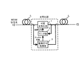
図1は、本発明による波長間光パワー偏差のモニタ方法が適用された第1実施形態としての光等化器について、その基本構成を示すブロック図である。
【0025】
図1において、本光等化器は、可変光等化手段としての可変光等化部1と、モニタ部2と、チャネル情報取得手段としての監視信号処理部3と、を備えて構成される。
【0026】
可変光等化部1は、光伝送路Lを伝搬する主信号光(WDM信号光)が入力され、該入力光パワーの波長に対する偏差(チルト)を可変の透過(または光フィルタ)特性に従って平坦化して出力する。この可変光等化部1としては、例えば、音響光学効果や磁気光学効果を利用した可変の通過波長特性を有する光フィルタ(特願平11−54374号参照)を利用してもよい。また、例えば、ラマン増幅を利用して光パワーの波長特性を補償する技術(特願平11−115971号参照)を利用することも可能である。なお、本発明で用いる可変光等化部1は上記の構成に限定されるものではなく公知の光等化器を用いることができる。
【0027】
モニタ部2は、可変光等化部1から出力されたWDM信号光の一部を分岐して、本発明のモニタ方法により光パワー偏差を測定し、その測定結果を基に可変光等化部1の特性を制御する。
【0028】
監視信号処理部3は、WDM信号光と共に伝送される監視信号光からチャネル情報を抽出してモニタ部2に伝える。このチャネル情報は、WDM信号光に含まれる各チャネルの波長位置およびビットレート(伝送速度)に関する情報を示すものである。
【0029】
ここで、本発明のモニタ方法を実現するモニタ部2の構成について詳しく説明する。
図2は、モニタ部2の具体的な構成例を示すブロック図である。
【0030】
図2に示すモニタ部2は、例えば、光パワー測定手段としての光パワー測定部20、波長域設定手段としての測定波長域設定部21および制御手段としての演算処理部22を有する。
【0031】
光パワー測定部20は、可変光等化部1からモニタ部2に入力されるWDM信号光の一部をモニタ入力光として、測定波長域設定部21からの出力信号により指定された測定波長域についての光パワーを測定し、該測定結果を演算処理部22に出力する。この光パワー測定部20の具体的な構成としては、例えば、文献「K.Otsuka et at.,“A High-Performance Optical Spectrum Monitor with High-Speed Measuring Time for WDM Optical Networks,” ECOC'97, Vol.2, pp.147-150(1997)」のFigure.1に記載された光学系などを応用するのが好適である。ここでは、その概容について簡単に説明する。
【0032】
図3は、上記文献の光学系を適用して構成した光パワー測定部20の具体例を示す図である。
図3に示す光パワー測定部20は、偏光補償板20A、第1レンズ20B、回折格子20C、第2レンズ20D、平面ミラー20EおよびPDアレイモジュール20F(受光部)を備え、これらの各光部品がいわゆるツエルニ−ターナーマウンティング(Czerny-Turner mounting)方法に従って配置された構成である。具体的には、入力光ファイバの一端から出射されたモニタ入力光が、偏光補償板20Aおよび第1レンズ20Bを介して回折格子20Cに送られ回折されて、さらに、その回折光は第2レンズ20Dを介して平面ミラー20Eに送られ反射された後に、PDアレイモジュール20Fによって受光される。
【0033】
PDアレイモジュール20Fは、例えば、モニタ入力光に含まれる複数のチャネル光の各波長にそれぞれ対応した複数の受光素子(PD)を有し、各PDの受光面が1平面内の所定位置に配列されている。ここでは、主信号光が最大32チャネルの光信号を含む場合を想定して、32個のPDがPDアレイモジュール20F内に設けられ、各PDが波長に応じて回折された各チャネル光の到達位置にそれぞれ対応させて配置される例を示す。
【0034】
図4は、各PDの相対的な出力特性を波長に対応させて模式的に示した図である。
図4のように、32個のPD1〜PD32は、チャネル1〜チャネル32の各波長を中心とする一定の波長範囲の光信号に対して略等しい出力電流をそれぞれ発生する。なお、上記一定の波長範囲は、各PDの配置および受光面の大きさに応じて決まるものであり、各PDに固有の受光波長に対応するものではない。各PDの受光波長としては、少なくとも対応するチャネル光の波長を含む範囲が必要があり、実用的には、32チャネルの光信号のすべての波長範囲に亘る受光波長を有するようにして、各々のPDに同じものを用いることが可能である。
【0035】
回折格子20Cは、断面が鋸歯状をした複数の溝を表面に有する、例えばホログラフィックブレーズドタイプ(holographic blazed type)等の回折格子である。偏光補償板20Aは、2つの複屈折楔から構成され、モニタ入力光を2つの直交する直線偏光成分に分離する。この偏光補償板20Aを設けることで、回折格子20Cの偏光依存性が排除される。このような光学系により、モニタ入力光に含まれる各チャネル光は、各々の波長に応じて回折されてPDアレイモジュール20Fの所定の位置に到達し、波長に対応したPDで電流にそれぞれ変換される。各PDの出力電流値は、測定波長域設定部21からの制御信号により指定された波長域に対応するものだけが選択されて演算処理部22に送られる。
【0036】
測定波長域設定部21は、監視信号処理部3からモニタ部2に入力されるチャネル情報を基に、光パワーを測定するのに最適な少なくとも2つの波長域を設定し、それらの測定波長域を指示する制御信号を光パワー測定部20に伝える。なお、測定波長域の設定方法については後述する。
【0037】
演算処理部22は、測定波長域設定部21からの制御信号に応じて設定された測定波長域についての光パワー比の目標値を求めると共に、光パワー測定部20からの出力電流値を用いて各測定波長域についての実際の光パワーの比を演算する。そして、光パワー比の測定値が目標比に等しくなるように可変光等化器1の特性を調整する制御信号を生成して、該制御信号を可変光等化器1に出力する。
【0038】
次に、上記のような構成の光等化器の動作を図5を用いて具体的に説明する。本光等化器では、まず、図5のフローチャートのステップ101(図中S101で示し、以下同様とする)において、監視信号光により伝達されるチャネル情報の抽出が監視信号処理部3で行われ、得られたチャネル情報がモニタ部2に伝えられる。ここでは、チャネル情報の具体的な一例として、伝送路Lを伝わるWDM信号光に含まれる各チャネルの番号が1,2,3,16,17,32であり、各チャネル光のビットレートがそれぞれ10Gb/sである場合を想定して、以下の説明を行うものとする。なお、チャネル1〜32は、いわゆる1550nm帯に所定の波長間隔で配置されている。また、ビットレートに対応して各チャネルに必要な光パワーが定まるものとし、上記のように各チャネルのビットレートが同じである場合には、すべてのチャネルの光パワーを略等しく制御することが求められる。
【0039】
チャネル情報の抽出が終了するとステップ102に進み、モニタ部2の測定波長域設定部21において、チャネル情報を基に、光パワーを測定するのに適した測定波長域の設定が行われる。ここでは、例えば、2つの測定波長域A,Bが設定されるものとする。測定波長域Aとしては、短波長側のチャネル1,2,3を含んだ波長1535.8〜1537.4nmが設定され、測定波長域Bとしては、長波長側のチャネル32を含んだ波長1560.6nmが設定される。そして、設定された測定波長域A,Bを示す制御信号が測定波長域設定部21から光パワー測定部20および演算処理部22に伝えられる。
【0040】
測定波長域の設定を行うときに留意すべき点としては、第1に、使用されるチャネルのうちの最短波長チャネルを含んだ波長域(第1測定波長域)および最長波長チャネルを含んだ波長域(第2測定波長域)を優先的に設定することが挙げられる。これは、各チャネル間の光パワーのばらつきは波長範囲が広くなるほど大きくなる傾向があるので、光パワーをモニタする2つの波長域の波長間隔をより広くすることで測定の精度を向上させることが可能になるためである。具体的には、上記の一例において、1550nm帯の中間に位置するチャネル16,17を含んだ波長域(以下、波長域Cとする)を測定波長域A,Bのいずれかに代えて設定することは測定精度を低下させる可能性がある。ただし、3つの測定波長域A,B,Cを設定した場合には、2つの測定波長域A,Bを設定した場合よりも測定精度は向上するものと考えられる。このように、本発明では、チャネル情報に応じて、最短波長チャネルおよび最長波長チャネルをそれぞれ含んだ少なくとも2つの測定波長域を設定することが必要である。
【0041】
また、第2に、雑音光を極力含まない波長域を設定することが挙げられる。これは、例えば本光等化器が用いられるシステムに適用された光増幅器で発生する広い帯域を持った自然放出光(雑音光)等によって、信号光パワーの測定に誤差が生じることを防ぐためである。具体的には、上記の一例において、隣接する使用チャネル1,2,3の波長範囲に限って測定波長域Aを設定することにより、使用されていないチャネル(例えばチャネル4,5等)まで波長域を広げた場合に比べて、雑音光の影響を低減させることが可能である。なお、測定波長域Aについて、最短波長のチャネル1だけでなくチャネル2,3を含むようにしたのは、隣接する使用チャネルをより多く含む方が信号光パワーの測定精度をより高くできるためである。
【0042】
なお、ステップ102において設定される2つの測定波長域が、予め設定した波長帯域よりも狭い帯域内にある場合、もしくは、設定可能な測定波長域が1つしか存在しない場合には、以下に示すステップ103以降の処理を行わずに可変光等化部1の制御を中断するようにしてもよい。これは、使用チャネル間の波長差が僅かであるので各チャネル間で生じる光パワーのばらつきが小さく、そのような光パワーのばらつきまでを等化する必要はないと判断できるためである。このようにすることで光等化器の制御を効率的に行うことが可能になる。
【0043】
次に、ステップ103では、演算処理部22において、各測定波長域A,Bについての光パワー比の目標値が求められる。ここでは、前述したように各チャネルのビットレートが同じであり各チャネルの光パワーをすべて同じ値となるように制御すればよいため、光パワー比の目標値は、各測定波長域A,Bに含まれるチャネル数に対応させて求めることができる。すなわち、測定波長域Aに含まれるチャネル数は3であり、測定波長域Bに含まれるチャネル数は1であるため、目標値となる光パワー比は、A:B=3:1(A/B=3)となる。
【0044】
目標値の演算が終了するか、または、目標値の演算と並行して、ステップ104では、各測定波長域A,Bにそれぞれ対応するPDの出力電流値の読み取りが行われる。具体的には、測定波長域設定部21からの制御信号を受けた光パワー測定部20が、測定波長域Aについてチャネル1〜チャネル3に対応するPD1〜PD3の各出力電流値、測定波長Bについてチャネル32に対応するPD32の出力電流値をそれぞれ演算処理部22に出力する。ここでは、例えば、PD1の出力電流値が0.5mA、PD2の出力電流値が0.6mA、PD3の出力電流値が0.7mAおよびPD32の出力電流値が1.0mAとなったものとする。
【0045】
そして、ステップ105では、光パワー測定部20からのモニタ値を受けた演算処理部22において、各測定波長域A,Bについての光パワー比の測定値が求められる。この測定値の演算は、各測定波長域に対応する各々のPDの出力電流値を加算し、該加算値の比を求めることにより行われる。上記のような各PDの出力電流値が得られた場合、測定波長域Aについては各PD1〜PD3の出力電流の加算値が1.8mAとなり、測定波長域BについてはPD32の出力電流値が1.0mAであるため、測定値となる光パワー比は、A:B=1.8:1(A/B=1.8)となる。
【0046】
測定値の演算が終了すると、ステップ106に進み、各測定波長域A,Bの光パワー比の測定値がステップ103で求めた目標値と等しくなるように、可変光等化部1の特性を調整する制御信号が演算処理部22で生成され光等化部1に送られる。これにより、光伝送路L等で発生する各チャネル間の光パワーの偏差が本光等化器によって確実に等化されるようになる。
【0047】
このように第1実施形態によれば、チャネル情報に基づいて、光パワーの測定に適した少なくとも2つの測定波長域を設定し、WDM信号光に含まれる各チャネルの光パワーの偏差をモニタするようにしたことで、比較的低い波長分解能により信号光パワーを直接測定しながら高い精度でチルトをモニタできるようになるため、簡略な構成で安価なモニタ部2を備えた光等化器を提供することが可能になる。
【0048】
次に、本発明の第2実施形態に係る光等化器のについて説明する。
第2実施形態では、上記第1実施形態の光等化器について、光パワー測定部20の構成をより簡略なものとして小型化を図った場合を考える。具体的には、第1実施形態の場合に、光パワー測定部20のPDアレイモジュール20Fが32チャネルの各信号光波長に対応して32個のPDを備えるものとしたが、第2実施形態では、個々のPDが受光する波長間隔が各チャネルの波長間隔よりも荒くなるようにすることで、チャネル数よりも少ない数のPDをPDアレイモジュールが備えるようにしたものである。
【0049】
図6は、第2実施形態で用いられるPDアレイモジュールについて、各PDの相対的な出力特性を波長に対応させて模式的に示した図である。なお、このPDアレイモジュールを用いて構成される光パワー測定部の構成は、上述の図3に示した場合と同様である。
【0050】
図6に示すように、第2実施形態で用いられるPDアレイモジュールには、例えば32チャネルの信号光に対して16個のPD1〜PD16が設けられる。ここでは、各PDの受光面がモニタ入力光の回折方向に沿って連続し、回折された奇数チャネルの信号光が各PDの受光面の中央部分に到達し、偶数チャネルの信号光が隣接するPDの境界部分に到達するように、各PD1〜PD16が所定位置に配置されている。このような配置では、例えば、チャネル1,2の各信号光がPD1で受光され、チャネル2,3,4の各信号光がPD2で受光され、以降同様にして、チャネル30,31,32の各信号光がPD16で受光されるようになる。
【0051】
上記のようなPDアレイモジュールが適用された光等化器の動作を図7を用いて説明する。
図7のにおいて、本光等化器の基本的な動作を示すフローチャートは、上述の図5に示した場合と同様である。ただし、PDアレイモジュールのPD数の減少に伴なって、具体例における、ステップ103での目標値の演算方法、ステップ104での出力電流値の読み取りが行われるPDおよびステップ105での測定値の演算方法について、それぞれ差異が生じる。
【0052】
すなわち、第1実施形態の場合と同様の具体例の設定において、ステップ103で目標値を求める場合、測定波長域Aに含まれるチャネル数は3であるが、チャネル2についてはPD1およびPD2の両方で受光され、図6に示したように各PD1,PD2で略等しい出力が発生するため、各測定波長域A,Bの光パワー比の目標値は、A:B=4:1(A/B=4)となる。
【0053】
また、ステップ104では、各測定波長域A,Bに対応させて、PD1,PD2およびPD16の各出力電流値の読み取りが行われる。ここでは、例えば、PD1の出力電流値が0.5mA、PD2の出力電流値が0.6mAおよびPD16の出力電流値が1.0mAとなったものとする。
【0054】
さらに、ステップ105では、各測定波長域A,Bについての光パワー比の測定値が求められ、ここでは、測定波長域AについてのPD1,2の出力電流の加算値が1.8mAとなり、測定波長域BについてのPD16の出力電流値が1.0mAであるため、光パワー比の測定値は、A:B=1.8:1(A/B=1.8)となる。そして、この測定値が目標値(A/B=4)に等しくなるように、ステップ106で可変光等化部1が制御される。
【0055】
このように第2実施形態によれば、光パワー測定部20のPDアレイモジュールの構成として、WDM信号光の最大チャネル数よりも少ない数のPDを設けるようにしても、第1実施形態の場合と同様の効果を得ることができる。したがって、モニタ部2の構成をより簡略なものにでき、光等化器の一層の小型化および低価格化を図ることが可能になる。
【0056】
なお、上記の第2実施形態では、32チャネルのWDM信号光に対して16個のPDを設ける場合を説明したが、本発明はこれに限らず、上記の場合と同様の考え方に従ってさらにPDの数を減らす応用も可能である。チルトモニタに要求される精度等に依存するが、最終的には、短波長側および長波長側の2つのPDを設けるだけでも本発明の効果を得ることは可能である。
【0057】
また、図6に示したように、各チャネルに対する各々のPDの相対出力が略等しくなるように16個のPDを配置する場合を示したが、例えば、図8(A)に示すように、奇数チャネルに対する各PDの相対出力が0dBとなり、偶数チャネルに対する各PDの相対出力が−3dB等となるような配置とすることも可能である。この場合、上記と同様の具体例についての光パワー比の目標値は、次のようにして演算すればよい。偶数チャネルの相対出力が−3dBということは、各PDで受光される偶数チャネルの光パワーが奇数チャネルの光パワーの1/2倍になることを意味する。このため、測定波長域Aについて、PD1ではチャネル1に対する出力値を1としてチャネル2に対する出力値が0.5となり、また、PD2ではチャネル2に対する出力値が0.5、チャネル3に対する出力値が1となる。一方、測定波長域Bについては、PD16でチャネル16に対する出力値が0.5となる。したがって、光パワー比の目標値は、A:B=(1+0.5+0.5+1):0.5=3:0.5=6:1になる。
【0058】
さらに、光等化器の小型化と低コスト化を目指して、図8(A)に示した場合よりもさらに少ないPDを用いてPDアレイモジュールを構成することも可能である。図8(B)はその一例を示すものである。
【0059】
図8(B)では、広い波長域の受光感度を有したPDが適用され、複数の波長の信号光が1つのPDで受光されると共に、各PDとも受光感度が最大になるポイントで信号光が受光される構成である。この場合、信号光の波長間隔(例えば0.8nm等)に対して、各PDの受光感度が最大になる受光帯域(例えば1.6nm以上)が広いことが必要となる。上記のようなPDアレイモジュールとした場合には、例えば、使用チャネル番号が3,4,6,7,9であることを示すチャネル情報が得られると、チャネル3,4を受光する短波長側のPD2およびチャネル9を受光する長波長側のPD4が選択されて、各々の電流値が読み取られる。ここでは、例えばPD2,pD4の各電流値が共に0.5mAであったとすると、それぞれの電流値を信号数で割った値、すなわち、PD2については0.5mA/2、PD4については0.5mA/1が求められ、両方の値が等しくなるように可変光等化部が調整される。
【0060】
加えて、各PDが受光する信号光の範囲は、図8(C)に示すように、隣り合うPDで重複するように設定しても構わない。すなわち、各測定波長域は、少なくとも1つの異なるチャネル光をそれぞれ含んでいればよい。図8(C)の場合には、例えばPD1とPD2においてチャネル3,4,5が重なることになる。
【0061】
次に、本発明の第3実施形態に係る光等化器について説明する。
図9は、第3実施形態に適用される光パワー測定部の構成を示すブロック図である。なお、光パワー測定部を除いた他の部分の光等化器の構成は、上述の図1および図2に示した第1実施形態の場合と同様である。
【0062】
図9において、本光等化器に用いられる光パワー測定部20’は、可変光フィルタとしてのチューナブル光フィルタ20G、受光部としてのフォトダイオード(PD)20Hおよび選択部としてのデータ記憶部20Iを有する。
【0063】
チューナブル光フィルタ20Gは、図示しない外部からの信号により通過波長特性を変化させることのできる公知の光フィルタであって、可変光等化部1から出力されたWDM信号光の一部を分岐したモニタ入力光が入力される。このチューナブル光フィルタ20Gの通過波長特性は、その通過中心波長が、測定波長域設定部21で設定される各測定波長域を含んだ波長範囲で時間的に変化するように制御されている。PD20Hは、チューナブル光フィルタ20Gを通過した光信号を電流に変換して出力する受光素子であって、ここでは、WDM信号光の波長帯域を含んだ広い受光波長を有する1つの受光素子が用いられるものとする。データ記憶部20Iは、PD20Hから出力される電流値を、その時のチューナブル光フィルタ20Gの通過中心波長に対応させて記憶するものであって、ここでは、測定波長域設定部21から出力される制御信号に従った各測定波長域に対応するデータだけを記憶すると共に、その記憶データを演算処理部22に出力する。
【0064】
上記のような光パワー測定部20’を適用した光等化器の動作を図10を用いて具体的に説明する。
図10において、ステップ101〜ステップ103の処理は、第1実施形態の場合と同様の処理が行われるため説明を省略する。ステップ103で目標値の演算が終了すると、ステップ201に進む。
【0065】
ステップ201では、光パワー測定部20’において、PD20Hの出力電流値が、チューナブル光フィルタ20Gの通過波長特性に対応させてデータ記憶部20Iに記憶される。このときデータ記憶部20Iに記憶される電流値は、測定波長域設定部21からの制御信号によって指示される各測定波長域A,Bに含まれる各チャネル1,2,3,32にそれぞれ対応したものだけが記憶され、他のチャネル4〜31に対応する電流値は記憶されない。ここでは、例えば、チューナブル光フィルタ20Gの通過中心波長が、チャネル1の波長に対応した時のPD20Hの出力電流値が0.5mA、チャネル2の波長に対応した時の電流値が0.6mA、チャネル3の波長に対応した時の電流値が0.7mA、チャネル32の波長に対応した時の電流値が1.0mAになるものとし、これらの電流値がデータ記憶部20Iに記憶されると共に演算処理部22に送られる。
【0066】
そして、演算処理部22では、第1実施形態の場合と同様にして、ステップ105で各測定波長域A,Bについての光パワー比の測定値がA:B=1.8:1と求められ、ステップ106で測定値が目標値と等しくなるように可変光等化部1の制御が行われる。
【0067】
このように第3実施形態によれば、チューナブル光フィルタ20G、PD20Hおよびデータ記憶部20Iを用いて光パワー測定部20’を構成するようにしても、第1実施形態の場合と同様の効果を得ることができる。また、チューナブル光フィルタ20Gの通過波長特性の半値幅はモニタする波長分解能に依存するが、適切な波長域を設定して光パワーの測定を行う本発明のモニタ方法では、比較的低い波長分解能でも光パワーを精度良くモニタでき、半値幅が狭い高度な光フィルタ特性を必要としないため、コスト面で有利になる。具体的には、例えば各チャネルの波長間隔が1nmという狭い間隔であるシステムにおいてでも、本モニタ方法を用いることで、例えば5nm程度の広い半値幅の通過波長特性を有したチューナブル光フィルタ20Gを適用できる。
【0068】
なお、上述の第1〜3実施形態では、各チャネルのビットレートが同じであって、各チャネルの光パワーがすべて同じ値となるように制御すればよい場合を示したが、各チャネルのビットレートが異なる場合についても本発明を適用することが可能である。この場合、各チャネルの光パワーの目標出力レベルは、それぞれのビットレートに対応して定まるため、この目標出力レベルの差を考慮して光パワー比の目標値を演算するようにする。具体的には、例えば、10Gb/sのチャネルの目標出力レベルが7dBm/chであり、2.5Gb/sのチャネルの目標出力レベルが4dBm/chである場合には、10Gb/sのチャネル光パワーに対して2.5Gb/sのチャネル光パワーが1/2倍となるようにして演算を行う。
【0069】
次に、本発明による波長間光パワー偏差のモニタ方法が適用された光増幅器について説明する。
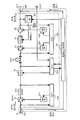
図11は、本発明の第4実施形態に係る光増幅器の構成を示すブロック図である。
【0070】
図11において、本光増幅器は、上述の第1〜3実施形態で示したいずれかの光等化器を公知の光増幅器に適用したものであって、例えば、実質的に2段構成とした光増幅部の段間に可変光減衰器(VAT)を配置した公知の構成の光増幅器に対して、本発明によるモニタ方法を適用したモニタ部60と、該モニタ部60のモニタ結果を応じて制御される可変利得等化器(VGEQ)61と、を設けたものである。
【0071】
2段構成の光増幅部は、例えばエルビウムドープ光ファイバ増幅器(EDFA)等が使用され、ここでは、前段の光増幅部が1つのEDFA51を有し、後段の光増幅部が直列に接続された2つのEDFA52,52’を有するものとする。なお、後段の光増幅部を2段のEDFA52,52’で構成したが、これは光増幅器の高出力化を実現するために後段の光増幅部をさらに2段構成としただけであって、実質的には1つのEDFAと考えても構わない。
【0072】
各EDFA51,52,52’それぞれは、各励起光源51A,52A,52A’からの励起光の供給を受けて励起状態とされたエルビウムドープ光ファイバ(EDF)内に、1550nm帯のWDM信号光を入射させ通過させることによって、各波長の信号光を一括して増幅する。なお、各EDFAの励起光波長は、980μm帯または1480μm帯等とすることができる。
【0073】
また、前段および後段の各光増幅部には、利得を一定に制御するAGC回路51B,52Bがそれぞれ設けられている。各AGC回路51B,52Bは、該当する光増幅部への入力光及び出力光の各パワーをモニタし、その光増幅部における利得が所要の値となるように励起光パワーの自動制御を行う。
【0074】
さらに、前段のEDFA51の出力側には、利得等化器(GEQ)51Cが設けられる。この利得等化器51Cは、EDFA51の利得波長特性に対応した固定の利得等化特性を有していて、EDFA51において発生する光パワーのチルトの補償を行う。また、後段側のEDFA52,52’の間には、可変利得等化手段としての可変利得等化器(VGEQ)61が設けられる。この可変利得等化器61は、モニタ部60のモニタ結果に応じて、WDM信号光のチルトを補償する可変の利得等化特性を有するものであって、上述の各第1〜3実施形態における光等化部1と同様の機能を備えたものである。なお、ここでは、可変利得等化器61は、EDFA52,52’の各利得波長特性に対応させて設計された基本的な利得等化特性を有し、その利得等化特性が、本光増幅器に接続される光伝送路等の損失波長特性によって発生する線形的なチルトの変動に応じて、変化可能となるように設計されているものとする。
【0075】
モニタ部60は、EDFA52’の出力光の一部を入力して、後述する監視信号処理部54からのチャネル情報に従った測定波長域についての光パワーを測定してモニタ光の光パワー偏差を求め、その結果に応じて可変利得等化器61の利得等化特性を調整する制御信号を発生する。このモニタ部60は、上述の各第1〜3実施形態におけるモニタ部2と同様のものである。なお、モニタ部60および可変利得等化器61の配置は、上記の位置に限定されるものではなく、可変利得等化器61の挿入損失等を考慮し、本光増幅器の雑音特性や出力光パワーなどに対する要求に応じて、適切な位置に設けることが可能である。
【0076】
前段および後段の光増幅部の段間には、可変光減衰器(VAT)53が設けられる。可変光減衰器53は、外部からの信号により光減衰量を変化させることのできる公知の光減衰器である。この可変光減衰器53の光減衰量は、ALC回路53Aから出力される信号によって制御される。ALC回路53Aは、可変光減衰器53の出力光の一部を分岐した光信号と、EDFA52’の出力光の一部を分岐し光カプラ53Bを介して送られてくる光信号とに基づいて、本光増幅器の1波長あたりの出力光パワーが一定のレベルとなるように可変光減衰器53の光減衰量を制御する信号を発生する。なお、光カプラ53Bで分岐された光信号は、AGC回路52Bにも送られると共に、出力モニタポートOUT’を介して外部にも出力される。
【0077】
また、本光増幅器は、入力されるWDM信号光に含まれる監視信号の処理を行う監視信号処理部54を有する。この監視信号処理部54は、入力ポートINと前段の光増幅部の間に挿入されたWDMカプラ54AによってWDM信号光から分波された監視信号光を入力し、該監視信号光を基にWDM信号光についてのチャネル情報等を得るものであって、上述の各第1〜3実施形態における監視信号処理3と同様の機能を備えるものである。ここでは、得られたチャネル情報がモニタ部60およびALC回路53Aに送られる。また、監視信号処理部54に入力された監視信号光は、後段の光増幅部と出力ポートOUTの間に挿入されたWDMカプラ54Bを介してWDM信号光に合波されて本光増幅器から出力される。
【0078】
さらに、ここでは本光増幅器に接続される光伝送路等で生じる波長分散を補償するための分散補償ファイバ(DCF)55が、例えば可変光減衰器53とEDFA52の間に接続されている。なお、この分散補償ファイバ55は、分散補償の必要性に応じて設ければよい。
【0079】
次に、上記のような構成を有する光増幅器の動作について説明する。
本光増幅器では、入力ポートINに入力されたWDM信号光が、EDFA51に送られると共に、その一部が分岐されAGC回路51Bに送られる。また、入力光に含まれる監視信号光がWDMカプラ54Aによって分波され監視信号処理部54に伝えられる。
【0080】
EDFA51では、励起光源51Aからの励起光の供給を受けて各波長の信号光が一括して増幅される。そして、EDFA51の出力光は、利得等化器51C、可変光減衰器53および分散補償ファイバ55を介して後段側のEDFA52に送られると共に、その一部が分岐されてAGC回路51Bに送られる。AGC回路51Bでは、EDFA51への入力光パワーおよびEDFA51からの出力光パワーをモニタして、EDFA51が利得一定で動作するように励起光源51Aの動作が制御される。
【0081】
また、チャネル情報取得手段としての監視信号処理部54では、WDMカプラ54Aで分波された監視信号光を基に、本光増幅器に入力されたWDM信号光についてのチャネル情報の識別が行われる。識別されたチャネル情報はモニタ部60に送られると共に、WDM信号光のチャネル数がALC回路53Aに伝えられる。
【0082】
EDFA52に送られたWDM信号光は、AGC回路52Aの制御下で一括増幅された後に、可変利得等化器60において利得等化され、さらに、EDFA52’に送られてAGC回路52A’の制御下で一括増幅される。このときの可変利得等化器60の利得等化特性は、モニタ部60から出力される制御信号に従って制御されており、この利得等化特性の制御動作は、上述の各実施形態における可変光等化部1の制御動作と同様のものである。すなわち、上述の図5などに示したモニタ方法と同様にして、各測定波長域についての光パワー比の目標値および測定値がモニタ部60でそれぞれ求められ、その測定値が目標値に等しくなるように可変利得等化器60の利得等化特性が制御される。
【0083】
さらに、本光増幅器では、EDFA52’の出力光の一部及び可変光減衰器53の出力光の一部がそれぞれ分岐されてALC回路53Aに送られ、可変光減衰器53の光減衰量がALC回路53Aによって制御される。これにより、1波長あたりの出力光パワーが一定に制御されたWDM信号光が出力ポートOUTを介して外部に出力されるようになる。
【0084】
このように第4実施形態によれば、本発明に係るモニタ方法を適用したモニタ部60および可変利得等化器61を光増幅器内に設けたことで、高い波長分解能を必要としない簡易な構成のモニタ部60により信号光のパワーを直接測定しながら高い精度でチルトをモニタできるようになる。これにより、小型でかつ低価格のチルト補償機能付きの光増幅器を提供することができる。
【0085】
なお、上記の第4実施形態では、可変利得等化器61が後段の光増幅部および光伝送路等で発生するチルトに対応した利得等化特性を有するものとして説明したが、このような可変の利得等化特性を1つの光等化器で実現するのが困難な場合には、例えば図12に示すように、利得等化特性が固定の利得等化器(GEQ)61’と可変利得等化器(VGEQ)61”とを組み合わせるようにしてもよい。この場合、固定の利得等化器61’の利得等化特性については、EDFA52,52’の複雑な利得波長特性に対応させて設計し、可変利得等化器61”の利得波長特性については、光伝送路等で発生する線形的なチルトに対応させて設計することが可能である。
【0086】
次に、本発明の第5実施形態に係る光増幅器について説明する。
図13は、第5実施形態の光増幅器の構成を示すブロック図である。
図13において、本光増幅器は、前述の図12に示した第4実施形態の構成について、前段側のEDFA51で発生するチルトを補償する固定の利得等化器51Cに代えて、可変利得等化器(VGEQ)63を設けると共に、該可変利得等化器63の利得等化特性を制御する、本発明のモニタ方法を用いたモニタ部62を設けたものである。
【0087】
可変利得等化器63は、EDFA51の利得波長特性に対応させて設計された基本的な利得等化特性を有し、その利得等化特性が、本光増幅器に接続される光伝送路等の損失波長特性によって発生する線形的なチルトの変動に応じて、変化可能となるように設計されているものとする。
【0088】
モニタ部62は、可変利得等化器63の出力光の一部を入力して、監視信号処理部54からのチャネル情報に従った測定波長域についての光パワーを測定してモニタ光の光パワー偏差を求め、その結果に応じて可変利得等化器63の利得等化特性を調整する制御信号を発生する。
【0089】
かかる構成の光増幅器では、入力ポートINに入力されたWDM信号光が、EDFA51に送られて一括増幅された後に、可変利得等化器63により利得等化される。このときの可変利得等化器63の利得等化特性は、モニタ部62から出力される制御信号に従って制御されている。モニタ部62においては、前述した後段側のモニタ部60の動作と同様に、監視信号処理部54からのチャネル情報に応じて各測定波長域についての光パワー比の目標値および測定値がそれぞれ求められ、その測定値が目標値に等しくなるように可変利得等化器63の利得等化特性が制御される。可変利得等化器63を通過したWDM信号光は、可変光減衰器53および分散補償ファイバ55を介して後段の光増幅部に送られ、前述した第4実施形態の場合と同様の動作が行われる。
【0090】
このように第5実施形態によれば、前段の光増幅部についても本発明のモニタ方法を適用したモニタ部62および可変利得等化器63を設けるようにしたことで、WDM信号光の利得等化がより確実に行われる光増幅器を提供することが可能になる。
【0091】
なお、上記の第5実施形態では、可変利得等化器63が前段の光増幅部および光伝送路等で発生するチルトに対応した利得等化特性を有するものとして説明したが、このような可変の利得等化特性を1つの光等化器で実現するのが困難な場合には、図14に示すように、EDFA51の複雑な利得波長特性に対応させて設計した固定の利得等化特性を有する利得等化器(GEQ)63’と、光伝送路等で発生する線形的なチルトに対応させて設計した可変の利得等化特性を有する利得等化器(VGEQ)63”とを組み合わせるようにしてもよい。なお、図14には、後段側についても固定および可変の利得等化器を組み合わせた場合の一例が示してある。もちろん、前段側および後段側のいずれかのみを組み合わせによる利得等化器としても構わない。
【0092】
次に、本発明の第6実施形態に係る光増幅器について説明する。
第6実施形態では、超広帯域な大容量増幅中継伝送を実現できる手段として有力視されている、光増幅帯域の異なる2種類以上の光増幅部が並列に接続された公知の光増幅器に対して、本発明のモニタ方法を適用して利得等化を行う場合を考える。
【0093】
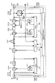
図15は、第6実施形態の光増幅器の構成を示すブロック図である。
図15において、本光増幅器は、例えば、入力されるWDM信号光を1530〜1570nm(以下、1550nm帯とする)および1570〜1610nm(以下、1580nm帯とする)の2つの増幅波長帯に分波する分波手段としての分波カプラ70と、該分波カプラ70で分波された1550nm帯の信号光を増幅する1550nm帯用光増幅部71と、分波カプラ70で分波された1580nm帯の信号光を増幅する1580nm帯用光増幅部72と、各光増幅部71,72から出力される信号光を合波する合波手段としての合波カプラ73と、を有する公知の構成に対して、各光増幅部71,72への入力光の一部がそれぞれ入力される入力モニタ部80と、分波カプラ70の入力側前段に挿入され、入力モニタ部80からの制御信号に従って可変の利得等化特性が調整される可変利得等化手段としての可変光等化器81と、を設けたものである。なお、ここでは、1550nm帯用光増幅部71および1580nm帯用光増幅部72が光増幅手段に相当し、入力モニタ部80が入力パワー測定手段および制御手段として機能する。
【0094】
1550nm帯用光増幅部71としては、1550nm帯に増幅帯域を有するエルビウムドープ光ファイバ増幅器(EDFA)等の一般的な光増幅器を用いることが可能である。また、1580nm帯用光増幅部72としては、例えば、1550nm帯用EDFAのエルビウムドープ光ファイバ長を長くするなどして、1580nm帯で光増幅作用が生じるようにした光増幅器などを用いることが可能である。
【0095】
入力モニタ部80は、1550nm帯用光増幅部71への入力光の一部を分岐したモニタ光を受光して、1550nm帯WDM信号光のトータル入力パワーをモニタすると共に、1580nm帯用光増幅部72への入力光の一部を分岐したモニタ光を受光して、1580nm帯WDM信号光のトータル入力パワーをモニタする機能を備える。なお、このトータル入力パワーのモニタ機能は、各光増幅部71,72に具備された入力モニタ機能(例えば、AGCのための入力モニタ機能など)を併用して、構成の簡略化を図ることが可能である。また、入力モニタ部80は、各光増幅部71,72内に設けられた図示しない監視信号処理部などによって識別されたチャネル情報に応じて、各光増幅部71,72についてのトータル入力パワーの比の目標値を算出して、この目標値と実際に測定した測定値とが等しくなるように、可変利得等化器81の利得等化特性を調整する制御信号を出力する。
【0096】
可変利得等化器81は、本光増幅器に接続される光伝送路等の損失波長特性に対応させて設計された可変の利得等化特性を有するものであって、上述の各第1〜3実施形態における光等化部1と同様の機能を備えたものである。
【0097】
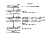
次に、上記のような構成の光増幅器の動作を図16を用いて具体的に説明する。
本光増幅器では、まず、図16のフローチャートのステップ301において、監視信号光により伝達されるチャネル情報の識別が行われ、該チャネル情報が入力モニタ部80に伝えられる。ここでは、チャネル情報の具体的な一例として、WDM信号光に含まれる各チャネルの番号が1,2,32,35,64であり、各チャネル光のビットレートがそれぞれ10Gb/sである場合を想定して、以下の説明を行うものとする。なお、チャネル1〜32は1550nm帯に所定の波長間隔で配置され、チャネル33〜64は1580nm帯に所定の波長間隔で配置されている。
【0098】
ステップ302では、入力モニタ部81において、チャネル情報を基に各光増幅部71,72についてのトータル入力パワー比の目標値が求められる。ここでは、1550nm帯に3つのチャネルが含まれ、1580nm帯には2つのチャネルが含まれるため、目標値となるトータル入力パワー比は、1550nm帯:1580nm帯=3:2となる。
【0099】
目標値の演算が終了するか、または、目標値の演算と並行して、ステップ303では、入力モニタ部80において各光増幅部へのトータル入力パワーが実際に測定されて、各光増幅部71,72についてのトータル入力パワー比の測定値が求められる。ここでは、例えば、各光増幅部71,72へのトータル入力パワーに対応する受光電流値が共に3mAであったとすると、トータル入力パワー比の測定値は、1550nm帯:1580nm帯=1:1となる。
【0100】
測定値の演算が終了すると、ステップ304に進み、各光増幅部71,72のトータル入力パワー比の測定値が目標値と等しくなるように、可変利得等化器81の利得等化特性を調整する制御信号が入力モニタ部80で生成され可変利得等化器81に送られる。これにより、本光増幅器に接続される光伝送路等で発生するチルトが確実に等化され、各チャネルについて光パワーの揃ったWDM信号光が分波カプラ70を介して各波長帯の光増幅部71,72に入力されるようになる。そして、各光増幅部71,72において増幅された各々の信号光は、合波カプラ73で合波されて、本光増幅器の外部に出力される。
【0101】
このように第6実施形態によれば、光増幅帯域の異なる2種類の光増幅部を並列に接続した光増幅器に対して、各光増幅部のトータル入力パワーをモニタする入力モニタ部80を設け、該入力モニタ部80で求めた各光増幅部のトータル入力パワー比の測定値が目標値と等しくなるように、本光増幅器の入力端に設けた可変利得等化器81の利得等化特性を制御するようにしたことで、各光増幅部に入力される信号光のチルトを簡易なモニタ方法を用いて確実に補償することができる。特に、広い波長帯域のWDM信号光を増幅する場合において、誘導ラマン散乱効果等により発生する光伝送路の損失波長特性を光増幅器の入力側で低減しておくことは、雑音指数の改善という観点からも有用である。
【0102】
なお、上記の第6実施形態では、各チャネルのビットレートが同じである場合を示したが、各チャネルのビットレートが異なる場合についても本発明を適用することが可能である。具体的には、図17に示すように、ステップ301で得られるチャネル情報が、例えば、チャネル1,3,35,64の各ビットレートについて10Gb/s(目標出力レベル;7dBm/ch)を示し、チャネル32のビットレートについて2.5Gb/s(目標出力レベル;4dBm/ch)を示す場合には、10Gb/sのチャネル光パワーに対する2.5Gb/sのチャネル光パワーが1/2倍となるため、ステップ302で求められる各光増幅器についてのトータル入力パワー比の目標値は、1550nm帯:1580nm帯=2.5:2=1.25:1となる。
【0103】
また、各チャネルのビットレートが同一であって目標出力レベルが同じである場合においては、チャネル情報の簡易化を図ることも可能である。すなわち、1550nm帯についてのチャネル数および1580nm帯についてのチャネル数をチャネル情報が含んでいれば十分とすることができる。この場合には、例えば図18に示すように、ステップ401で得られる各波長帯のチャネル数と、ステップ402で測定される各光増幅部についてのトータル入力パワーとを用い、ステップ403において各光増幅部の平均入力パワーの比を求め、該平均入力パワーの比が1550nm帯:1580nm帯=1:1になるように、ステップ404で可変利得等化器81の利得等化特性を制御すればよい。
【0104】
さらに、上述の第6実施形態では、1550nm帯および1580nm帯の2つの光増幅部を並列に設けた場合について説明したが、本発明はこれに限らず、増幅帯域の異なる3種類以上の光増幅部を並列に接続した光増幅器に対しても、上述の場合と同様にして応用することが可能である。
【0105】
【発明の効果】
以上説明したように、本発明の波長間光パワー偏差のモニタ方法は、WDM信号光についてのチャネル情報を基に、測定に適した少なくとも2つの測定波長域を設定し、該各測定波長域に限ってチャネル光パワーを測定して波長間光パワー偏差を判断するようにしたことで、比較的低い波長分解能によっても高い精度でWDM信号光パワーの波長特性をモニタすることができる。また、WDM信号光の等化処理のフィードバック制御を行う光等化器および光増幅器に本発明のモニタ方法を適用することで、各機器の小型化および低価格化を図ることが可能になる。
【図面の簡単な説明】
【図1】本発明の第1実施形態に係る光等化器の構成を示すブロック図である。
【図2】同上第1実施形態におけるモニタ部の構成例を示すブロック図である。
【図3】同上第1実施形態における光パワー測定部の具体例を示す図である。
【図4】同上第1実施形態におけるPDアレイモジュールの各PDの相対的な出力特性を模式的に示した図である。
【図5】同上第1実施形態の動作を説明するフローチャートである。
【図6】本発明の第2実施形態におけるPDアレイモジュールの各PDの相対的な出力特性を模式的に示した図である。
【図7】同上第2実施形態の動作を説明するフローチャートである。
【図8】同上第2実施形態に関連する他の構成のPDアレイモジュールについて、各PDの相対的な出力特性を模式的に示した図である。
【図9】本発明の第3実施形態における光パワー測定部の具体例を示すブロック図である。
【図10】同上第3実施形態の動作を説明するフローチャートである。
【図11】本発明の第4実施形態に係る光増幅器の構成を示すブロック図である。
【図12】同上第4実施形態に関連して、固定および可変の利得等化器を組み合わせて用いた場合の構成を示すブロック図である。
【図13】本発明の第5実施形態に係る光増幅器の構成を示すブロック図である。
【図14】同上第5実施形態に関連して、固定および可変の利得等化器を組み合わせて用いた場合の構成を示すブロック図である。
【図15】本発明の第6実施形態に係る光増幅器の構成を示すブロック図である。
【図16】同上第6実施形態の動作を説明するフローチャートである。
【図17】同上第6実施形態に関連して、各チャネルのビットレートが異なる場合の動作を説明するフローチャートである。
【図18】同上第6実施形態に関連して、各チャネルのビットレートが同じ場合にチャネル情報の簡易化を図ったときの動作を説明するフローチャートである。
【符号の説明】
1…可変光等化部
2…モニタ部
3…監視信号処理部
20,20’…光パワー測定部
20C…回折格子
20F…PDアレイモジュール
20G…チューナブル光フィルタ
20H…受光素子(PD)
20I…データ記憶部
21…測定波長域設定部
22…演算処理部
51,52,52’…光増幅部(EDFA)
54…監視信号処理部
60,62…モニタ部
61,63,81…可変利得等化器(VGEQ)
70…分波カプラ
71…1550nm帯用光増幅部
72…1580nm帯用光増幅部
73…合波カプラ
80…入力モニタ部[0001]
BACKGROUND OF THE INVENTION
The present invention relates to a method for monitoring an optical power deviation between wavelengths, which accurately monitors the wavelength characteristics of optical power of wavelength division multiplexed (WDM) signal light used in various optical communications, and to monitor the same. The present invention relates to an optical equalizer and an optical amplifier that control an equalization process of wavelength characteristics of optical power of WDM signal light using a method.
[0002]
[Prior art]
In optical communication, research and development of a wavelength division multiplexing (WDM) transmission system that increases communication capacity by transmitting light of a plurality of wavelengths through a single optical fiber has become active. This WDM transmission system can use existing optical fiber, so the introduction cost is low, and the use of an optical amplifier with a wide amplification band makes the transmission line bit-rate free and facilitates future upgrades. It has advantages and is expected as a means to realize a future multimedia society.
[0003]
In general, in a WDM optical communication system using an optical amplifier, in order to obtain predetermined transmission characteristics, it is necessary to transmit the optical power with a deviation (tilt) of each channel being suppressed to several dB or less in each amplification relay stage. is there. This is because the upper limit of the optical power that can be transmitted is limited by waveform deterioration due to the nonlinear effect of the optical transmission path, and the lower limit is limited by deterioration of the reception S / N.
[0004]
However, in an optical fiber transmission line, it is known that a wavelength characteristic occurs in the loss due to stimulated Raman scattering or Rayleigh scattering, which is one of nonlinear effects. In particular, the loss wavelength characteristic due to stimulated Raman scattering depends on various transmission conditions such as the length of the optical transmission line, the number of channels (number of wavelengths of signal light), channel spacing (wavelength spacing of signal light), optical power level, and the like. , Occur in different sizes. In general, the number of channels and the wavelength used in a WDM optical transmission system can be set as appropriate by the system user, so their values are not always constant. For example, in a lightwave network or the like, the number and wavelength position of signal light input to an optical ADM (Optical Add and Drop Multiplexer) device dynamically change, and therefore, loss wavelength characteristics having different sizes are generated in the optical transmission line. As a result, the influence on the transmission characteristics becomes a serious problem.
[0005]
In addition, optical amplifiers and dispersion compensators that constitute various optical communication systems are also known to have wavelength characteristics in gain and loss. There is a problem that a deviation occurs in the power and greatly affects the transmission characteristics.
[0006]
Therefore, it is required to monitor the optical power deviation between the channels generated in the WDM optical communication system and take measures to reduce this deviation. In contrast, the present inventor, for example, applies an active gain equalizer to a WDM optical communication system, so that the monitor value of the deviation of the optical power between the channels becomes small. Techniques for controlling characteristics have been proposed (see Japanese Patent Application Nos. 11-54374 and 11-115971).
[0007]
As a conventional monitoring method for monitoring the optical power deviation between channels applied to the above-mentioned invention of the prior application, for example, the optical power between channels based on spontaneous emission (ASE) light generated by an optical amplifier. (See Japanese Patent Application No. 11-054374). In this method, since the spontaneous emission light power in the vicinity of the signal light band is monitored, it is possible to monitor the variation in the optical power between channels without depending on the number of input signals or channel fluctuations. In addition, for example, a method of directly measuring the optical power of each channel using a general optical spectrum analyzer or the like and calculating the optical power deviation between channels is also known.
[0008]
[Problems to be solved by the invention]
However, the monitoring method using spontaneous emission among the conventional methods for monitoring optical power deviation between wavelengths is an indirect method of monitoring spontaneous emission rather than directly monitoring signal light itself. Therefore, there is a possibility that a monitor error occurs. As for the monitoring method for directly measuring each signal light power using an optical spectrum analyzer or the like, for example, even when the signal light is input most densely in the signal light band, it is necessary to accurately measure each signal light power. Therefore, it is necessary to measure the signal light power using a high performance optical spectrum analyzer or the like having an excellent wavelength resolution. Therefore, the apparatus to which this monitoring method is applied has a problem in that the cost increases and the size increases.
[0009]
The present invention has been made paying attention to the above points, and directly monitors the signal light power without requiring high wavelength resolution, and detects the optical power deviation between channels with high accuracy, and An object of the present invention is to provide an optical equalizer and an optical amplifier which are reduced in size and price by applying the monitoring method.
[0010]
[Means for Solving the Problems]
In order to achieve the above object, an inter-wavelength optical power deviation monitoring method according to the present invention is based on a process of obtaining channel information regarding WDM signal light in which a plurality of channel lights having different wavelengths are wavelength-multiplexed, and based on the channel information. A process of setting a plurality of measurement wavelength regions including at least one different channel light, a step of measuring the channel light power of the WDM signal light only for each measurement wavelength region, and a measured value of the optical power And determining the optical power deviation between the wavelengths of the WDM signal light by obtaining the optical power ratio for each measurement wavelength region.
[0011]
According to such a monitoring method, at least two measurement wavelength ranges suitable for optical power measurement are set based on channel information regarding the wavelength position and transmission speed of each channel light included in the WDM signal light, and each measurement The channel optical power is measured only in the wavelength range, and the optical power deviation between wavelengths is determined from the optical power ratio for each measurement wavelength range based on the measurement result. As a result, the wavelength characteristics of the WDM signal light power can be monitored with high accuracy while directly measuring the signal light power even at a relatively low wavelength resolution.
[0012]
For a plurality of measurement wavelength regions including at least one different channel light, each measurement wavelength region has one channel light, and each channel light is different from each other, and there are a plurality of measurement wavelength regions. Each of the plurality of channel lights, and at least one of the plurality of channel lights can be different from each other, and a plurality of measurement wavelength ranges can be obtained by combining the two cases. .
[0013]
In the above monitoring method, the process of setting the measurement wavelength range includes at least setting a first measurement wavelength range including the shortest wavelength channel light and a second measurement wavelength range including the longest wavelength channel light among the input channels. You may make it do. It is desirable to set each measurement wavelength region so that the ratio including noise light is minimized. By doing in this way, it becomes possible to improve the measurement accuracy of the optical power deviation of each channel light.
[0014]
Further, in the process of obtaining channel information, specifically, based on the monitoring signal light transmitted along with the WDM signal light, the channel information including the wavelength position and transmission speed of each channel light of the WDM signal light is obtained. You may make it obtain.
[0015]
The optical equalizer according to the present invention is an optical equalizer that equalizes the wavelength characteristics of the optical power of WDM signal light in which a plurality of channel lights having different wavelengths are wavelength-multiplexed, and has variable optical equalization characteristics. Variable optical equalization means to which WDM signal light is input, channel information acquisition means for obtaining channel information about the WDM signal light, and at least one different channel light based on the channel information obtained by the channel information acquisition means Wavelength setting means for setting a plurality of measurement wavelength bands included, and light for measuring the channel light power of the WDM signal light that has passed through the variable light equalization means only for each measurement wavelength band set by the wavelength band setting means Based on the channel information obtained by the power measurement means and the channel information acquisition means, the target value of the optical power ratio for each measurement wavelength range that flattens the optical power wavelength characteristic of the WDM signal light is obtained. In both cases, the measurement result of the optical power measurement means is used to obtain a measurement value of the optical power ratio for each measurement wavelength range, and the optical equalization characteristics of the variable light equalization means are set so that the measurement value is substantially equal to the target value. And control means for controlling.
[0016]
Also, an aspect of the optical amplifier according to the present invention is an optical amplifier including an optical amplifying unit that collectively amplifies WDM signal light in which a plurality of channel lights having different wavelengths are wavelength-multiplexed. Variable gain equalization means to which WDM signal light is input, channel information acquisition means for obtaining channel information about the WDM signal light, and at least one different based on the channel information obtained by the channel information acquisition means The wavelength optical power of the WDM signal light that has passed through the variable gain equalization means is set only for the wavelength range setting means for setting a plurality of measurement wavelength ranges including the channel light, and for each measurement wavelength range set by the wavelength range setting means. Based on the optical power measurement means to be measured and the channel information obtained by the channel information acquisition means, the optical power wavelength characteristics of the WDM signal light are flattened for each measurement wavelength range. Obtain the target value of the power ratio, obtain the measured value of the optical power ratio for each measurement wavelength region using the measurement result of the optical power measuring means, and adjust the variable gain, etc. so that the measured value is substantially equal to the target value. Control means for controlling the gain equalization characteristics of the equalizing means.
[0017]
In the optical equalizer or the optical amplifier having such a configuration, the monitoring method according to the present invention described above is realized by the operations of the channel information acquisition unit, the wavelength band setting unit, the optical power measurement unit, and the control unit, and according to the monitoring result. Thus, the equalization characteristic of the variable light equalization means or the variable gain equalization means is feedback controlled. This makes it possible to provide a small and inexpensive optical equalizer or optical amplifier that can reliably perform equalization processing of the optical power wavelength characteristics of WDM signal light.
[0018]
Furthermore, as a specific configuration of the optical equalizer or the optical amplifier, the optical power measurement unit includes a diffraction grating that generates a diffracted light when a part of the WDM signal light that has passed through the variable optical equalization unit is incident, Measurement of optical power in the light receiving element corresponding to each measurement wavelength range set by the wavelength range setting means, having a plurality of light receiving elements arranged corresponding to the arrival position of each channel light diffracted by the diffraction grating A light receiving unit that selects the result and transmits it to the control means. In addition, the light receiving unit may have two or more light receiving elements which are equal to or less than the maximum number of channels included in the WDM signal light.
[0019]
In the optical power measuring means having such a configuration, each channel light power is measured for each corresponding light receiving element using the diffraction of light by the diffraction grating, and the measurement result of the light receiving element corresponding to each measurement wavelength region is selectively used. Is transmitted to the control means.
[0020]
Alternatively, as another specific configuration of the optical power measurement means, a part of the WDM signal light that has passed through the variable light equalization means is input, and according to each measurement wavelength range set by the wavelength range setting means, A variable optical filter in which the center wavelength of the pass band changes with time, a light receiving unit that measures the power of the channel light that has passed through the variable optical filter, and each of the measurement results in the light receiving unit set by the wavelength band setting means And a selection unit that selects data corresponding to the measurement wavelength range and transmits the data to the control unit.
[0021]
In the optical power measuring means having such a configuration, the power of each channel light is measured by the light receiving unit according to the time change of the pass band of the variable optical filter, and the light reception when the pass band of the variable optical filter corresponds to the measurement wavelength range. The measurement result of the element is selectively transmitted to the control means.
[0022]
As another aspect of the optical amplifier according to the present invention, a demultiplexing unit that demultiplexes WDM signal light in which a plurality of channel lights having different wavelengths are wavelength-multiplexed into at least two amplification wavelength bands, and In an optical amplifier comprising at least two optical amplifying means for amplifying the optical signals in each amplified wavelength band that have been demultiplexed, and multiplexing means for multiplexing the optical signals amplified by the respective optical amplifying means, Variable gain equalization means that has variable gain equalization characteristics and is provided upstream of the input side of the demultiplexing means, channel information acquisition means for obtaining channel information about the WDM signal light, and input to each optical amplification means Based on the channel information obtained by the input power measuring means for inputting a part of the optical signal in each amplification wavelength band and measuring the total input power to each optical amplifying means and the channel information obtaining means, the WDM signal light Light power While obtaining the target value of the total input power ratio for each optical amplifying means for flattening the wavelength characteristics, and determining the measured value of the total input power ratio for each optical amplifying means using the measurement result of the input power measuring means, Control means for controlling the gain equalization characteristic of the variable gain equalization means so that the measured value is substantially equal to the target value.
[0023]
In the optical amplifier having such a configuration, the WDM signal light having a wide signal light band is sent to the demultiplexing unit via the variable gain equalization unit and demultiplexed into a plurality of amplification wavelength bands. The demultiplexed optical signals in the respective amplification wavelength bands are respectively amplified by the corresponding optical amplification means, and then multiplexed by the multiplexing means. At this time, a part of each optical signal input to each optical amplifying means is sent to the input power measuring means to monitor the total input power, and according to the monitoring result, a variable gain provided in the input stage, etc. The gain equalization characteristic of the equalizing means is feedback-controlled by the control means. In this case, each amplification wavelength band corresponds to each measurement wavelength band of the above-described monitoring method, and the monitoring method according to the present invention is realized by the operations of the channel information acquisition means, the input power measurement means, and the control means. This makes it possible to reliably compensate for the tilt of the input light to each optical amplifying means having different amplification wavelength bands using a simple monitoring method. There are two points in this configuration. The first point is that the tilt is compensated on the input side of the optical amplifying means. Therefore, in order to relieve the noise figure of the channel in which the transmission optical power is degraded, not only the tilt compensation of the optical amplifier but also the wavelength characteristic of the noise figure is improved. In other words, the optical SNR also works advantageously. The second point is that a function for monitoring input power is already applied to a normal optical amplifier, and a part of the input light is branched and the branched light power is received by a photodiode. . Since this monitoring method uses this, it is not necessary to insert a new optical component.
[0024]
DETAILED DESCRIPTION OF THE INVENTION
Hereinafter, embodiments of the present invention will be described with reference to the drawings.
FIG. 1 is a block diagram showing a basic configuration of an optical equalizer as a first embodiment to which a method for monitoring an optical power deviation between wavelengths according to the present invention is applied.
[0025]
In FIG. 1, this optical equalizer includes a variable
[0026]
The variable
[0027]
The monitor unit 2 branches a part of the WDM signal light output from the variable
[0028]
The monitoring
[0029]
Here, the configuration of the monitor unit 2 that implements the monitoring method of the present invention will be described in detail.
FIG. 2 is a block diagram illustrating a specific configuration example of the monitor unit 2.
[0030]
The monitor unit 2 illustrated in FIG. 2 includes, for example, an optical
[0031]
The optical
[0032]
FIG. 3 is a diagram illustrating a specific example of the optical
The optical
[0033]
The
[0034]
FIG. 4 is a diagram schematically showing the relative output characteristics of each PD corresponding to the wavelength.
As shown in FIG. 4, the 32 PD1 to PD32 respectively generate substantially equal output currents for optical signals in a certain wavelength range centered on the wavelengths of the
[0035]
The
[0036]
The measurement wavelength
[0037]
The
[0038]
Next, the operation of the optical equalizer configured as described above will be specifically described with reference to FIG. In this optical equalizer, first, in step 101 of the flowchart of FIG. 5 (indicated by S101 in the figure, the same shall apply hereinafter), channel information transmitted by the monitoring signal light is extracted by the monitoring
[0039]
When the extraction of the channel information is completed, the process proceeds to step 102 where the measurement wavelength
[0040]
The points to be noted when setting the measurement wavelength range are as follows. First, of the channels used, the wavelength range including the shortest wavelength channel (first measurement wavelength range) and the wavelength including the longest wavelength channel. An example is to set the area (second measurement wavelength area) with priority. This is because the variation in the optical power between the channels tends to increase as the wavelength range becomes wider, so that the measurement accuracy can be improved by increasing the wavelength interval between the two wavelength ranges for monitoring the optical power. This is because it becomes possible. Specifically, in the above example, the wavelength region including the channels 16 and 17 located in the middle of the 1550 nm band (hereinafter referred to as the wavelength region C) is set in place of either the measurement wavelength region A or B. This can reduce the measurement accuracy. However, when three measurement wavelength regions A, B, and C are set, it is considered that the measurement accuracy is improved as compared with the case where two measurement wavelength regions A and B are set. Thus, in the present invention, it is necessary to set at least two measurement wavelength ranges each including the shortest wavelength channel and the longest wavelength channel according to the channel information.
[0041]
Second, setting a wavelength region that contains as little noise light as possible. This is to prevent an error in measuring the signal light power due to, for example, spontaneous emission light (noise light) having a wide band generated by an optical amplifier applied to a system in which the present optical equalizer is used. It is. Specifically, in the above example, by setting the measurement wavelength band A only in the wavelength range of the adjacent
[0042]
Note that, when the two measurement wavelength bands set in step 102 are within a narrower band than the preset wavelength band, or when there is only one settable measurement wavelength band, the following is shown. You may make it interrupt control of the variable
[0043]
Next, in step 103, the
[0044]
In step 104, the output current value of the PD corresponding to each of the measurement wavelength regions A and B is read in parallel with the calculation of the target value or in parallel with the calculation of the target value. Specifically, the optical
[0045]
In step 105, the
[0046]
When the calculation of the measurement value is completed, the process proceeds to step 106, and the characteristics of the variable
[0047]
As described above, according to the first embodiment, at least two measurement wavelength ranges suitable for optical power measurement are set based on channel information, and the optical power deviation of each channel included in the WDM signal light is monitored. By doing so, it becomes possible to monitor the tilt with high accuracy while directly measuring the signal light power with a relatively low wavelength resolution, so that an optical equalizer having a simple configuration and an inexpensive monitor unit 2 is provided. It becomes possible to do.
[0048]
Next, an optical equalizer according to a second embodiment of the present invention will be described.
In the second embodiment, consider a case where the optical equalizer of the first embodiment is downsized by simplifying the configuration of the optical
[0049]
FIG. 6 is a diagram schematically showing the relative output characteristics of each PD corresponding to the wavelength in the PD array module used in the second embodiment. The configuration of the optical power measurement unit configured using this PD array module is the same as that shown in FIG.
[0050]
As shown in FIG. 6, the PD array module used in the second embodiment is provided with, for example, 16 PD1 to PD16 for 32-channel signal light. Here, the light receiving surface of each PD is continuous along the diffraction direction of the monitor input light, the diffracted odd-channel signal light reaches the central portion of the light-receiving surface of each PD, and the even-channel signal light is adjacent. Each PD1 to PD16 is arranged at a predetermined position so as to reach the boundary portion of the PD. In such an arrangement, for example, the signal lights of
[0051]
The operation of the optical equalizer to which the above PD array module is applied will be described with reference to FIG.
In FIG. 7, the flowchart showing the basic operation of the present optical equalizer is the same as that shown in FIG. However, as the number of PDs in the PD array module decreases, the calculation method of the target value in step 103, the PD from which the output current value is read in step 104, and the measured value in step 105 in the specific example There are differences in the calculation methods.
[0052]
That is, in the setting of a specific example similar to the case of the first embodiment, when the target value is obtained in step 103, the number of channels included in the measurement wavelength band A is 3, but for channel 2, both PD1 and PD2 6 and substantially equal outputs are generated in the PD1 and PD2, as shown in FIG. 6, the target value of the optical power ratio in each of the measurement wavelength regions A and B is A: B = 4: 1 (A / B = 4).
[0053]
In step 104, the output current values of PD1, PD2, and PD16 are read in correspondence with the measurement wavelength ranges A and B. Here, for example, it is assumed that the output current value of PD1 is 0.5 mA, the output current value of PD2 is 0.6 mA, and the output current value of PD16 is 1.0 mA.
[0054]
Further, in step 105, the measured value of the optical power ratio for each of the measurement wavelength regions A and B is obtained, and here, the added value of the output currents of PD1 and PD2 for the measurement wavelength region A is 1.8 mA, Since the output current value of the PD 16 for the wavelength band B is 1.0 mA, the measured value of the optical power ratio is A: B = 1.8: 1 (A / B = 1.8). Then, in step 106, the variable
[0055]
As described above, according to the second embodiment, the PD array module of the optical
[0056]
In the second embodiment, the case where 16 PDs are provided for 32 channels of WDM signal light has been described. However, the present invention is not limited to this, and the PD is further configured in accordance with the same concept as described above. Applications that reduce the number are also possible. Although depending on the accuracy required for the tilt monitor, it is finally possible to obtain the effects of the present invention simply by providing two PDs on the short wavelength side and the long wavelength side.
[0057]
In addition, as shown in FIG. 6, the case where 16 PDs are arranged so that the relative outputs of the respective PDs with respect to the respective channels are substantially equal is shown. For example, as shown in FIG. It is also possible to arrange such that the relative output of each PD with respect to the odd channel is 0 dB, and the relative output of each PD with respect to the even channel is −3 dB. In this case, the target value of the optical power ratio for a specific example similar to the above may be calculated as follows. The relative output of the even channel being −3 dB means that the optical power of the even channel received by each PD is ½ times the optical power of the odd channel. For this reason, in the measurement wavelength range A, the output value for
[0058]
Furthermore, with the aim of reducing the size and cost of the optical equalizer, it is also possible to construct a PD array module using fewer PDs than in the case shown in FIG. FIG. 8B shows an example.
[0059]
In FIG. 8B, a PD having a light receiving sensitivity in a wide wavelength range is applied, and signal light having a plurality of wavelengths is received by one PD, and at each point the light receiving sensitivity is maximized for each PD. Is configured to receive light. In this case, it is necessary that the light receiving band (for example, 1.6 nm or more) at which the light receiving sensitivity of each PD is maximized is wide with respect to the wavelength interval of the signal light (for example, 0.8 nm). In the case of the PD array module as described above, for example, when channel information indicating that the used channel numbers are 3, 4, 6, 7, and 9 is obtained, the short wavelength side that receives the
[0060]
In addition, the range of signal light received by each PD may be set so that adjacent PDs overlap as shown in FIG. That is, each measurement wavelength region only needs to include at least one different channel light. In the case of FIG. 8C, for example,
[0061]
Next, an optical equalizer according to a third embodiment of the present invention will be described.
FIG. 9 is a block diagram illustrating a configuration of an optical power measurement unit applied to the third embodiment. The configuration of the optical equalizer in the other parts excluding the optical power measurement unit is the same as that in the first embodiment shown in FIGS. 1 and 2 described above.
[0062]
In FIG. 9, an optical
[0063]
The tunable
[0064]
The operation of the optical equalizer to which the optical
In FIG. 10, the processing from step 101 to step 103 is the same as that in the first embodiment, and a description thereof will be omitted. When the calculation of the target value is completed in step 103, the process proceeds to step 201.
[0065]
In
[0066]
Then, in the
[0067]
As described above, according to the third embodiment, even when the optical
[0068]
In the first to third embodiments described above, the bit rate of each channel is the same, and the optical power of each channel may be controlled to have the same value. The present invention can be applied even when the rates are different. In this case, since the target output level of the optical power of each channel is determined corresponding to each bit rate, the target value of the optical power ratio is calculated in consideration of the difference in the target output level. Specifically, for example, when the target output level of a 10 Gb / s channel is 7 dBm / ch and the target output level of a 2.5 Gb / s channel is 4 dBm / ch, 10 Gb / s channel light is used. The calculation is performed so that the 2.5 Gb / s channel light power is ½ times the power.
[0069]
Next, an optical amplifier to which the inter-wavelength optical power deviation monitoring method according to the present invention is applied will be described.
FIG. 11 is a block diagram showing a configuration of an optical amplifier according to the fourth embodiment of the present invention.
[0070]
In FIG. 11, the present optical amplifier is one in which any of the optical equalizers shown in the first to third embodiments is applied to a known optical amplifier, and has, for example, a substantially two-stage configuration. A
[0071]
For example, an erbium-doped optical fiber amplifier (EDFA) or the like is used as the two-stage optical amplifying unit. Here, the preceding optical amplifying unit has one
[0072]
Each
[0073]
In addition,
[0074]
Further, a gain equalizer (GEQ) 51C is provided on the output side of the
[0075]
The
[0076]
A variable optical attenuator (VAT) 53 is provided between the stages of the preceding and succeeding optical amplifying units. The variable
[0077]
The optical amplifier further includes a monitoring
[0078]
Further, here, a dispersion compensating fiber (DCF) 55 for compensating for chromatic dispersion generated in an optical transmission line connected to the present optical amplifier is connected between the variable
[0079]
Next, the operation of the optical amplifier having the above configuration will be described.
In this optical amplifier, the WDM signal light input to the input port IN is sent to the
[0080]
In the
[0081]
Further, the monitoring
[0082]
The WDM signal light sent to the
[0083]
Furthermore, in this optical amplifier, a part of the output light of the
[0084]
As described above, according to the fourth embodiment, the
[0085]
In the fourth embodiment, the
[0086]
Next, an optical amplifier according to a fifth embodiment of the invention will be described.
FIG. 13 is a block diagram illustrating a configuration of the optical amplifier according to the fifth embodiment.
In FIG. 13, the present optical amplifier replaces the fixed
[0087]
The
[0088]
The
[0089]
In the optical amplifier having such a configuration, the WDM signal light input to the input port IN is sent to the
[0090]
As described above, according to the fifth embodiment, the
[0091]
In the fifth embodiment, the
[0092]
Next, an optical amplifier according to a sixth embodiment of the present invention will be described.
In the sixth embodiment, compared to a known optical amplifier in which two or more types of optical amplification units having different optical amplification bands are connected in parallel, which is regarded as a promising means for realizing ultra-wideband large-capacity amplification relay transmission. Consider a case where gain equalization is performed by applying the monitoring method of the present invention.
[0093]
FIG. 15 is a block diagram illustrating a configuration of an optical amplifier according to the sixth embodiment.
In FIG. 15, this optical amplifier demultiplexes input WDM signal light into two amplification wavelength bands of 1530 to 1570 nm (hereinafter referred to as 1550 nm band) and 1570 to 1610 nm (hereinafter referred to as 1580 nm band), for example. A
[0094]
As the
[0095]
The
[0096]
The
[0097]
Next, the operation of the optical amplifier configured as described above will be specifically described with reference to FIG.
In this optical amplifier, first, in step 301 of the flowchart of FIG. 16, channel information transmitted by the monitoring signal light is identified, and the channel information is transmitted to the
[0098]
In step 302, the
[0099]
In step 303, the total input power to each optical amplifying unit is actually measured by the
[0100]
When the calculation of the measurement value is completed, the process proceeds to step 304, and the gain equalization characteristic of the
[0101]
Thus, according to the sixth embodiment, the
[0102]
In the sixth embodiment, the case where the bit rate of each channel is the same is shown, but the present invention can be applied to the case where the bit rate of each channel is different. Specifically, as shown in FIG. 17, the channel information obtained in step 301 indicates, for example, 10 Gb / s (target output level; 7 dBm / ch) for each bit rate of
[0103]
Further, when the bit rate of each channel is the same and the target output level is the same, the channel information can be simplified. That is, it is sufficient if the channel information includes the number of channels for the 1550 nm band and the number of channels for the 1580 nm band. In this case, for example, as shown in FIG. 18, the number of channels in each wavelength band obtained in step 401 and the total input power for each optical amplification unit measured in step 402 are used. If the ratio of the average input power of the amplifying unit is obtained, and the gain equalization characteristic of the
[0104]
Furthermore, in the above-described sixth embodiment, the case where the two optical amplifying units of the 1550 nm band and the 1580 nm band are provided in parallel has been described. However, the present invention is not limited to this, and three or more types of optical amplification having different amplification bands The present invention can also be applied to an optical amplifier having parts connected in parallel in the same manner as described above.
[0105]
【The invention's effect】
As described above, the inter-wavelength optical power deviation monitoring method according to the present invention sets at least two measurement wavelength ranges suitable for measurement based on channel information about the WDM signal light, and sets each measurement wavelength range. By measuring the channel optical power only to determine the optical power deviation between wavelengths, the wavelength characteristic of the WDM signal light power can be monitored with high accuracy even with a relatively low wavelength resolution. Further, by applying the monitoring method of the present invention to an optical equalizer and an optical amplifier that perform feedback control of equalization processing of WDM signal light, it becomes possible to reduce the size and price of each device.
[Brief description of the drawings]
FIG. 1 is a block diagram showing a configuration of an optical equalizer according to a first embodiment of the present invention.
FIG. 2 is a block diagram showing a configuration example of a monitor unit in the first embodiment.
FIG. 3 is a diagram showing a specific example of an optical power measurement unit in the first embodiment.
FIG. 4 is a diagram schematically showing a relative output characteristic of each PD of the PD array module in the first embodiment.
FIG. 5 is a flowchart for explaining the operation of the first embodiment.
FIG. 6 is a diagram schematically showing a relative output characteristic of each PD of the PD array module in the second embodiment of the present invention.
FIG. 7 is a flowchart for explaining the operation of the second embodiment.
FIG. 8 is a diagram schematically showing the relative output characteristics of each PD in a PD array module having another configuration related to the second embodiment.
FIG. 9 is a block diagram illustrating a specific example of an optical power measurement unit according to a third embodiment of the present invention.
FIG. 10 is a flowchart for explaining the operation of the third embodiment.
FIG. 11 is a block diagram showing a configuration of an optical amplifier according to a fourth embodiment of the present invention.
FIG. 12 is a block diagram showing a configuration when a fixed and variable gain equalizer is used in combination in relation to the fourth embodiment;
FIG. 13 is a block diagram showing a configuration of an optical amplifier according to a fifth embodiment of the present invention.
FIG. 14 is a block diagram showing a configuration when a fixed and variable gain equalizer is used in combination in association with the fifth embodiment.
FIG. 15 is a block diagram showing a configuration of an optical amplifier according to a sixth embodiment of the present invention.
FIG. 16 is a flowchart for explaining the operation of the sixth embodiment;
FIG. 17 is a flowchart for explaining the operation when the bit rates of the respective channels are different in relation to the sixth embodiment.
FIG. 18 is a flowchart for explaining the operation when the channel information is simplified when the bit rate of each channel is the same in relation to the sixth embodiment.
[Explanation of symbols]
1 ... Variable light equalization section
2 ... Monitor section
3. Monitoring signal processing unit
20, 20 '... Optical power measurement unit
20C ... Diffraction grating
20F ... PD array module
20G ... Tunable optical filter
20H: Light receiving element (PD)
20I: Data storage unit
21 ... Measurement wavelength range setting section
22 ... arithmetic processing part
51, 52, 52 '... Optical amplifier (EDFA)
54. Monitoring signal processing unit
60, 62 ... monitor section
61, 63, 81 ... Variable gain equalizer (VGEQ)
70: demultiplexing coupler
71 ... 1550nm band optical amplifier
72 .. 1580 nm band optical amplifier
73 ... Multiplexing coupler
80: Input monitor section
Claims (14)
該チャネル情報に基づいて、少なくとも1つの異なるチャネル光を含んだ複数の測定波長域を設定する過程と、
該各測定波長域についてのみ、前記WDM信号光のチャネル光パワーを測定する過程と、
該光パワーの測定値を用いて前記各測定波長域についての光パワー比を求め、WDM信号光の波長間光パワー偏差を判断する過程と、
を含んでなることを特徴とする波長間光パワー偏差のモニタ方法。Obtaining channel information about WDM signal light in which a plurality of channel lights having different wavelengths are multiplexed;
Setting a plurality of measurement wavelength ranges including at least one different channel light based on the channel information;
Measuring the channel optical power of the WDM signal light only for each of the measurement wavelength ranges;
Determining the optical power ratio for each of the measurement wavelength regions using the measured value of the optical power, and determining the optical power deviation between wavelengths of the WDM signal light;
A method for monitoring an optical power deviation between wavelengths, comprising:
前記測定波長域を設定する過程は、最短波長チャネル光を含んだ第1測定波長域と、最長波長チャネル光を含んだ第2測定波長域とを少なくとも設定することを特徴とする波長間光パワー偏差のモニタ方法。The monitoring method according to claim 1,
The step of setting the measurement wavelength range includes setting at least a first measurement wavelength range including the shortest wavelength channel light and a second measurement wavelength range including the longest wavelength channel light. Deviation monitoring method.
前記測定波長域を設定する過程は、雑音光を含む割合が最小となるように各測定波長域を設定することを特徴とする波長間光パワー偏差のモニタ方法。The monitoring method according to claim 1,
The method of monitoring the optical power deviation between wavelengths, wherein in the step of setting the measurement wavelength range, each measurement wavelength range is set so that the ratio including noise light is minimized.
前記チャネル情報を得る過程は、WDM信号光に伴なって伝達される監視信号光を基に、前記WDM信号光の各チャネル光の波長位置および伝送速度を含んだ前記チャネル情報を得ることを特徴とする波長間光パワー偏差のモニタ方法。The monitoring method according to claim 1,
In the process of obtaining the channel information, the channel information including the wavelength position and transmission speed of each channel light of the WDM signal light is obtained based on the monitoring signal light transmitted along with the WDM signal light. The inter-wavelength optical power deviation monitoring method.
可変の光等化特性を有し、前記WDM信号光が入力される可変光等化手段と、
前記WDM信号光についてのチャネル情報を得るチャネル情報取得手段と、
該チャネル情報取得手段で得たチャネル情報に基づいて、少なくとも1つの異なるチャネル光を含んだ複数の測定波長域を設定する波長域設定手段と、
前記波長域設定手段で設定された各測定波長域についてのみ、前記可変光等化手段を通過したWDM信号光のチャネル光パワーを測定する光パワー測定手段と、
前記チャネル情報取得手段で得たチャネル情報を基に、前記WDM信号光の光パワー波長特性を平坦にする各測定波長域についての光パワー比の目標値を求めると共に、前記光パワー測定手段の測定結果を用いて前記各測定波長域についての光パワー比の測定値を求め、該測定値が前記目標値に略等しくなるように、前記可変光等化手段の光等化特性を制御する制御手段と、を含んで構成されたことを特徴とする光等化器。In an optical equalizer that equalizes wavelength characteristics of optical power of WDM signal light in which a plurality of channel lights having different wavelengths are wavelength-multiplexed,
Variable optical equalization means having variable optical equalization characteristics and receiving the WDM signal light;
Channel information obtaining means for obtaining channel information about the WDM signal light;
Wavelength range setting means for setting a plurality of measurement wavelength ranges including at least one different channel light based on channel information obtained by the channel information acquisition means;
Optical power measuring means for measuring the channel optical power of the WDM signal light that has passed through the variable optical equalization means only for each measurement wavelength band set by the wavelength band setting means,
Based on the channel information obtained by the channel information acquisition means, a target value of the optical power ratio for each measurement wavelength range for flattening the optical power wavelength characteristics of the WDM signal light is obtained, and the measurement of the optical power measurement means Control means for obtaining a measured value of the optical power ratio for each measurement wavelength region using the result and controlling the optical equalization characteristics of the variable light equalization means so that the measured value is substantially equal to the target value And an optical equalizer characterized in that the optical equalizer is configured to include.
前記光パワー測定手段は、前記可変光等化手段を通過したWDM信号光の一部が入射されて回折光を発生する回折格子と、
該回折格子で回折された各チャネル光の到達位置に対応させて配置された複数の受光素子を有し、前記波長域設定手段で設定された各測定波長域に対応する前記受光素子における光パワーの測定結果を選択して前記制御手段に伝える受光部と、を含むことを特徴とする光等化器。The optical equalizer according to claim 5, comprising:
The optical power measuring means includes a diffraction grating that generates diffracted light when a part of the WDM signal light that has passed through the variable light equalizing means is incident thereon,
Optical power in the light receiving element corresponding to each measurement wavelength range set by the wavelength range setting means, having a plurality of light receiving elements arranged corresponding to the arrival position of each channel light diffracted by the diffraction grating And a light receiving section that selects and transmits the measurement result to the control means.
前記受光部が、WDM信号光に含まれる最大チャネル数以下で、かつ、2個以上の受光素子を有することを特徴とする光等化器。The optical equalizer according to claim 6, comprising:
An optical equalizer, wherein the light receiving unit has two or more light receiving elements that are equal to or less than the maximum number of channels included in the WDM signal light.
前記光パワー測定手段は、前記可変光等化手段を通過したWDM信号光の一部が入力され、前記波長域設定手段で設定された各測定波長域に応じて、通過帯域の中心波長が時間変化する可変光フィルタと、
該可変光フィルタを通過したチャネル光のパワーを測定する受光部と、
該受光部における測定結果のうちで前記波長域設定手段で設定された各測定波長域に対応するデータを選択して前記制御手段に伝える選択部と、を含むことを特徴とする光等化器。The optical equalizer according to claim 5, comprising:
The optical power measurement means receives a part of the WDM signal light that has passed through the variable light equalization means, and the center wavelength of the pass band is set to a time according to each measurement wavelength range set by the wavelength range setting means. A variable optical filter that changes,
A light receiving unit for measuring the power of the channel light that has passed through the variable optical filter;
An optical equalizer comprising: a selection unit that selects data corresponding to each measurement wavelength range set by the wavelength range setting unit from the measurement results in the light receiving unit and transmits the data to the control unit .
可変の利得等化特性を有し、前記WDM信号光が入力される可変利得等化手段と、
前記WDM信号光についてのチャネル情報を得るチャネル情報取得手段と、
該チャネル情報取得手段で得たチャネル情報に基づいて、少なくとも1つの異なるチャネル光を含んだ複数の測定波長域を設定する波長域設定手段と、
前記波長域設定手段で設定された各測定波長域についてのみ、前記可変利得等化手段を通過したWDM信号光のチャネル光パワーを測定する光パワー測定手段と、
前記チャネル情報取得手段で得たチャネル情報を基に、前記WDM信号光の光パワー波長特性を平坦にする各測定波長域についての光パワー比の目標値を求めると共に、前記光パワー測定手段の測定結果を用いて前記各測定波長域についての光パワー比の測定値を求め、該測定値が前記目標値に略等しくなるように、前記可変利得等化手段の利得等化特性を制御する制御手段と、を含んで構成されたことを特徴とする光増幅器。In an optical amplifier provided with an optical amplifying means for collectively amplifying WDM signal light in which a plurality of channel lights having different wavelengths are wavelength-multiplexed,
Variable gain equalization means having variable gain equalization characteristics, to which the WDM signal light is input;
Channel information obtaining means for obtaining channel information about the WDM signal light;
Wavelength range setting means for setting a plurality of measurement wavelength ranges including at least one different channel light based on channel information obtained by the channel information acquisition means;
Optical power measurement means for measuring the channel optical power of the WDM signal light that has passed through the variable gain equalization means only for each measurement wavelength band set by the wavelength band setting means,
Based on the channel information obtained by the channel information acquisition means, a target value of the optical power ratio for each measurement wavelength range for flattening the optical power wavelength characteristics of the WDM signal light is obtained, and the measurement of the optical power measurement means Control means for obtaining a measured value of the optical power ratio for each measurement wavelength region using the result and controlling the gain equalization characteristics of the variable gain equalization means so that the measured value is substantially equal to the target value And an optical amplifier comprising:
前記光パワー測定手段は、前記可変利得等化手段を通過したWDM信号光の一部が入射されて回折光を発生する回折格子と、
該回折格子で回折された各チャネル光の到達位置に対応させて配置された複数の受光素子を有し、前記波長域設定手段で設定された各測定波長域に対応する前記受光素子における光パワーの測定結果を選択して前記制御手段に伝える受光部と、を含むことを特徴とする光増幅器。The optical amplifier according to claim 9, comprising:
The optical power measuring means includes a diffraction grating that generates diffracted light when a part of the WDM signal light that has passed through the variable gain equalizing means is incident thereon,
Optical power in the light receiving element corresponding to each measurement wavelength range set by the wavelength range setting means, having a plurality of light receiving elements arranged corresponding to the arrival position of each channel light diffracted by the diffraction grating And a light receiving unit that selects and transmits the measurement result to the control means.
前記受光部が、WDM信号光に含まれる最大チャネル数以下で、かつ、2個以上の受光素子を有することを特徴とする光等化器。The optical amplifier according to claim 10, comprising:
An optical equalizer, wherein the light receiving unit has two or more light receiving elements that are equal to or less than the maximum number of channels included in the WDM signal light.
前記光パワー測定手段は、前記可変利得等化手段を通過したWDM信号光の一部が入力され、前記波長域設定手段で設定された各測定波長域に応じて、通過帯域の中心波長が時間変化する可変光フィルタと、
該可変光フィルタを通過したチャネル光の光パワーを測定する受光部と、
該受光部における測定結果のうちで前記波長域設定手段で設定された各測定波長域に対応するデータを選択して前記制御手段に伝える選択部と、を含むことを特徴とする光増幅器。The optical amplifier according to claim 9, comprising:
The optical power measurement means receives a part of the WDM signal light that has passed through the variable gain equalization means, and the center wavelength of the pass band is set to a time according to each measurement wavelength band set by the wavelength band setting means. A variable optical filter that changes,
A light receiving unit for measuring the optical power of the channel light that has passed through the variable optical filter;
An optical amplifier comprising: a selection unit that selects data corresponding to each measurement wavelength range set by the wavelength range setting unit from the measurement results in the light receiving unit and transmits the data to the control unit.
可変の利得等化特性を有し、前記分波手段の入力側前段に設けられる可変利得等化手段と、
前記WDM信号光についてのチャネル情報を得るチャネル情報取得手段と、
前記各光増幅手段に入力される各増幅波長帯の光信号の一部を入力して、各光増幅手段へのトータル入力パワーをそれぞれ測定する入力パワー測定手段と、
前記チャネル情報取得手段で得たチャネル情報を基に、前記WDM信号光の光パワー波長特性を平坦にする各光増幅手段についてのトータル入力パワー比の目標値を求めると共に、前記入力パワー測定手段の測定結果を用いて前記各光増幅手段についてのトータル入力パワー比の測定値を求め、該測定値が前記目標値に略等しくなるように、前記可変利得等化手段の利得等化特性を制御する制御手段と、を含んで構成されたことを特徴とする光増幅器。A demultiplexing unit that demultiplexes WDM signal light, in which a plurality of channel lights having different wavelengths are wavelength-multiplexed, into at least two amplification wavelength bands, and an optical signal in each amplification wavelength band demultiplexed by the demultiplexing unit, respectively. In an optical amplifier comprising at least two optical amplifying means and a multiplexing means for multiplexing each optical signal amplified by each optical amplifying means,
Variable gain equalization means having variable gain equalization characteristics, provided in the input stage upstream of the branching means;
Channel information obtaining means for obtaining channel information about the WDM signal light;
Input power measuring means for measuring a total input power to each optical amplifying means by inputting a part of an optical signal of each amplification wavelength band inputted to each optical amplifying means,
Based on the channel information obtained by the channel information acquisition means, a target value of the total input power ratio for each optical amplification means for flattening the optical power wavelength characteristic of the WDM signal light is obtained, and the input power measurement means Using the measurement result, a measurement value of the total input power ratio for each of the optical amplification means is obtained, and the gain equalization characteristic of the variable gain equalization means is controlled so that the measurement value is substantially equal to the target value. And an optical amplifier characterized by comprising control means.
前記増幅波長帯は、1550nm帯および1580nm帯の波長帯を含むことを特徴とする光増幅器。The optical amplifier according to claim 13.
The amplification wavelength band includes a wavelength band of 1550 nm band and 1580 nm band.
Priority Applications (4)
| Application Number | Priority Date | Filing Date | Title |
|---|---|---|---|
| JP27501199A JP3803000B2 (en) | 1999-09-28 | 1999-09-28 | Method for monitoring optical power deviation between wavelengths, and optical equalizer and optical amplifier using the same |
| EP00115059A EP1089477B1 (en) | 1999-09-28 | 2000-07-26 | Inter-wavelength light power deviation monitoring method and optical equalizer and amplifier utilizing the method |
| DE60043566T DE60043566D1 (en) | 1999-09-28 | 2000-07-26 | Method for monitoring the deviation of the optical intermediate wavelength strength and optical equalizers and amplifiers using the method |
| US09/628,811 US6724526B1 (en) | 1999-09-28 | 2000-07-28 | Inter-wavelength light power deviation monitoring method and optical equalizer and optical amplifier utilizing the method |
Applications Claiming Priority (1)
| Application Number | Priority Date | Filing Date | Title |
|---|---|---|---|
| JP27501199A JP3803000B2 (en) | 1999-09-28 | 1999-09-28 | Method for monitoring optical power deviation between wavelengths, and optical equalizer and optical amplifier using the same |
Publications (2)
| Publication Number | Publication Date |
|---|---|
| JP2001103013A JP2001103013A (en) | 2001-04-13 |
| JP3803000B2 true JP3803000B2 (en) | 2006-08-02 |
Family
ID=17549648
Family Applications (1)
| Application Number | Title | Priority Date | Filing Date |
|---|---|---|---|
| JP27501199A Expired - Fee Related JP3803000B2 (en) | 1999-09-28 | 1999-09-28 | Method for monitoring optical power deviation between wavelengths, and optical equalizer and optical amplifier using the same |
Country Status (4)
| Country | Link |
|---|---|
| US (1) | US6724526B1 (en) |
| EP (1) | EP1089477B1 (en) |
| JP (1) | JP3803000B2 (en) |
| DE (1) | DE60043566D1 (en) |
Families Citing this family (32)
| Publication number | Priority date | Publication date | Assignee | Title |
|---|---|---|---|---|
| JP2002280966A (en) | 2001-03-21 | 2002-09-27 | Nec Miyagi Ltd | Insertion signal level setting system for oadm system, and setting method therefor |
| WO2003079584A1 (en) * | 2002-03-19 | 2003-09-25 | Fujitsu Limited | Method and system for optical fiber transmission using raman amplification |
| US7725042B2 (en) * | 2002-04-22 | 2010-05-25 | Marvin Ray Young | Automated optical transport system |
| US7831152B2 (en) | 2002-06-04 | 2010-11-09 | Finisar Corporation | Optical transceiver |
| US7505688B2 (en) | 2002-06-04 | 2009-03-17 | Finisar Corporation | Optical transceiver |
| US6774348B2 (en) | 2002-06-04 | 2004-08-10 | Honeywell International Inc. | Method and apparatus for monitoring the power of a multi-wavelength optical signal |
| JP3994275B2 (en) | 2002-07-22 | 2007-10-17 | 日本電気株式会社 | Optical direct amplifier |
| US6937798B1 (en) * | 2003-01-17 | 2005-08-30 | General Photonics Corporation | Optical spectrum monitor |
| JP3936958B2 (en) | 2003-06-27 | 2007-06-27 | 富士通株式会社 | Amplifying medium performance simulation apparatus and method, and optical amplifier |
| DE60302786T2 (en) * | 2003-08-18 | 2006-07-06 | Alcatel | Optical transmission method and optical receiver |
| US7369777B2 (en) * | 2003-11-20 | 2008-05-06 | General Instrument Corporation | Method and apparatus for automatically adjusting the optical power directed to a dispersion compensating element |
| US7526201B2 (en) * | 2004-06-25 | 2009-04-28 | Tyco Telecommunications (Us) Inc. | Optical fiber transmission system with noise loading |
| JP2006286918A (en) * | 2005-03-31 | 2006-10-19 | Furukawa Electric Co Ltd:The | Optical amplifier |
| US7693419B1 (en) | 2005-11-23 | 2010-04-06 | General Photonics Corporation | Optical spectrum analysis using optical interferometry |
| JP2008042096A (en) * | 2006-08-09 | 2008-02-21 | Fujitsu Ltd | Optical amplifier and light transmission system |
| JP4630256B2 (en) * | 2006-10-16 | 2011-02-09 | 古河電気工業株式会社 | Optical amplification method, apparatus thereof, and optical amplification repeater system using the apparatus |
| JP4859651B2 (en) * | 2006-12-14 | 2012-01-25 | 日本電信電話株式会社 | Optical amplifier and optical communication system |
| JP4985762B2 (en) | 2007-02-27 | 2012-07-25 | 富士通株式会社 | WDM transmission equipment |
| WO2009028042A1 (en) * | 2007-08-27 | 2009-03-05 | Fujitsu Limited | Network management system, and relay device and method |
| EP2225841B1 (en) | 2007-11-27 | 2013-07-24 | Telefonaktiebolaget LM Ericsson (publ) | Methods and systems for increasing reach and/or split in passive optical networks |
| US8345238B2 (en) * | 2008-02-04 | 2013-01-01 | General Photonics Corporation | Measuring optical spectral property of light based on polarization analysis |
| JP4941349B2 (en) * | 2008-02-19 | 2012-05-30 | 富士通株式会社 | Optical transmission device used in PON system |
| IL206722A0 (en) * | 2010-06-30 | 2010-12-30 | Eci Telecom Ltd | Technology for simulating and/or controlling communication optical networks |
| JP5703611B2 (en) * | 2010-07-07 | 2015-04-22 | 日本電気株式会社 | Signal light correction apparatus and signal light correction method |
| JP5644446B2 (en) * | 2010-12-06 | 2014-12-24 | 富士通株式会社 | Optical transmission equipment |
| JP2012156285A (en) | 2011-01-26 | 2012-08-16 | Fujitsu Ltd | Light amplifier |
| CN104104447B (en) * | 2013-04-10 | 2018-08-24 | 南京中兴新软件有限责任公司 | Light power equalization method and device |
| JP6294902B2 (en) * | 2016-03-10 | 2018-03-14 | 株式会社フジクラ | Coherent optical receiver and method for manufacturing coherent optical receiver |
| EP3637637A4 (en) * | 2017-07-07 | 2020-06-24 | Huawei Technologies Co., Ltd. | Optical amplification device, optical communication station, and optical communication system |
| JP7057501B2 (en) * | 2018-05-31 | 2022-04-20 | 日本電信電話株式会社 | Optical transmission control method and optical transmission system |
| EP4027540B1 (en) * | 2019-10-31 | 2024-01-24 | Huawei Technologies Co., Ltd. | Method for determining optical signal power change and power calculation device |
| JP2022045728A (en) * | 2020-09-09 | 2022-03-22 | 日本電気株式会社 | Optical transmission device, optical transmission method, and program |
Family Cites Families (10)
| Publication number | Priority date | Publication date | Assignee | Title |
|---|---|---|---|---|
| JP2871547B2 (en) | 1995-09-08 | 1999-03-17 | 日本電気株式会社 | Optical spectrum analyzer apparatus and optical amplifier control method |
| JP3422398B2 (en) * | 1995-12-07 | 2003-06-30 | 富士通株式会社 | Center-of-gravity wavelength monitoring method and apparatus, optical amplifier, and optical communication system |
| JP3883601B2 (en) | 1996-03-27 | 2007-02-21 | 富士通株式会社 | Optical equalizer |
| JPH09321701A (en) * | 1996-05-31 | 1997-12-12 | Fujitsu Ltd | Optical communication system and optical amplifier |
| US5915052A (en) * | 1997-06-30 | 1999-06-22 | Uniphase Telecommunications Products, Inc. | Loop status monitor for determining the amplitude of the signal components of a multi-wavelength optical beam |
| AU8802498A (en) * | 1997-08-01 | 1999-02-22 | Pirelli Cavi E Sistemi S.P.A. | Multi-band amplification system for dense wavelength division multiplexing |
| US6115157A (en) * | 1997-12-24 | 2000-09-05 | Nortel Networks Corporation | Methods for equalizing WDM systems |
| EP0933894B1 (en) * | 1998-01-27 | 2007-07-25 | Lucent Technologies Inc. | Method and system for controlling optical amplification in wavelength division multiplex optical transmission |
| EP0975103B1 (en) * | 1998-02-06 | 2006-08-09 | Fujitsu Limited | Optical amplifier and method for controlling an excitation light source in an optical amplifier |
| US6535330B1 (en) * | 2001-03-31 | 2003-03-18 | Corning Incorporated | Dynamic controller for a multi-channel optical amplifier |
-
1999
- 1999-09-28 JP JP27501199A patent/JP3803000B2/en not_active Expired - Fee Related
-
2000
- 2000-07-26 DE DE60043566T patent/DE60043566D1/en not_active Expired - Lifetime
- 2000-07-26 EP EP00115059A patent/EP1089477B1/en not_active Expired - Lifetime
- 2000-07-28 US US09/628,811 patent/US6724526B1/en not_active Expired - Lifetime
Also Published As
| Publication number | Publication date |
|---|---|
| EP1089477B1 (en) | 2009-12-23 |
| JP2001103013A (en) | 2001-04-13 |
| EP1089477A3 (en) | 2005-03-16 |
| EP1089477A2 (en) | 2001-04-04 |
| US6724526B1 (en) | 2004-04-20 |
| DE60043566D1 (en) | 2010-02-04 |
Similar Documents
| Publication | Publication Date | Title |
|---|---|---|
| JP3803000B2 (en) | Method for monitoring optical power deviation between wavelengths, and optical equalizer and optical amplifier using the same | |
| JP2834376B2 (en) | Signal processing device | |
| US6510000B1 (en) | Optical amplifier for wide band raman amplification of wavelength division multiplexed (WDM) signal lights | |
| JP3527671B2 (en) | Method of controlling wavelength characteristics of optical transmission power by Raman amplification, wavelength division multiplexing optical communication system and optical amplifier using the same | |
| US6034812A (en) | Gain equalizer and optical transmission system having the gain equalizer | |
| EP2180612B1 (en) | Control apparatus and method for optical transmission apparatus | |
| JP3638777B2 (en) | Method for gain equalization and apparatus and system used to implement the method | |
| US6654561B1 (en) | Method and apparatus for measuring optical signal-to-noise ratio, and pre-emphasis method and optical communication system each utilizing the method | |
| US6807376B2 (en) | Gain equalizer which includes a plurality of optical filters for equalizing the gain of an optical amplifier | |
| JP4626918B2 (en) | Raman optical repeater | |
| EP1381125B1 (en) | Method and device for optical amplification and system having the device | |
| JP4725951B2 (en) | Wavelength multiplexed signal light amplification method and optical amplifier | |
| EP1076434A2 (en) | Optical amplifying apparatus and method for amplifying wide-wavelength-band light | |
| EP1909414B1 (en) | Dynamic raman tilt compensation | |
| JP5245747B2 (en) | Optical amplifier and optical receiver module | |
| JP5267119B2 (en) | Optical receiver and wavelength division multiplexing transmission system | |
| US8139285B2 (en) | Raman amplifying device and control method | |
| US20120188631A1 (en) | Optical amplification apparatus | |
| JP4659498B2 (en) | Optical transmission equipment | |
| US20040240042A1 (en) | Optical amplifier, communication system and method for control tilt of a communication system | |
| JP2000269578A (en) | Method and device for light amplification and its system | |
| JPH11119030A (en) | Dispersion compensating device | |
| US7206124B2 (en) | Gain-providing optical power equalizer | |
| JP3482962B2 (en) | Optical amplifier and optical transmission system using the same | |
| JP2001144353A (en) | Optical amplifier |
Legal Events
| Date | Code | Title | Description |
|---|---|---|---|
| A621 | Written request for application examination |
Free format text: JAPANESE INTERMEDIATE CODE: A621 Effective date: 20040805 |
|
| A977 | Report on retrieval |
Free format text: JAPANESE INTERMEDIATE CODE: A971007 Effective date: 20060328 |
|
| TRDD | Decision of grant or rejection written | ||
| A01 | Written decision to grant a patent or to grant a registration (utility model) |
Free format text: JAPANESE INTERMEDIATE CODE: A01 Effective date: 20060425 |
|
| A61 | First payment of annual fees (during grant procedure) |
Free format text: JAPANESE INTERMEDIATE CODE: A61 Effective date: 20060501 |
|
| R150 | Certificate of patent or registration of utility model |
Free format text: JAPANESE INTERMEDIATE CODE: R150 |
|
| FPAY | Renewal fee payment (event date is renewal date of database) |
Free format text: PAYMENT UNTIL: 20090512 Year of fee payment: 3 |
|
| FPAY | Renewal fee payment (event date is renewal date of database) |
Free format text: PAYMENT UNTIL: 20100512 Year of fee payment: 4 |
|
| FPAY | Renewal fee payment (event date is renewal date of database) |
Free format text: PAYMENT UNTIL: 20100512 Year of fee payment: 4 |
|
| FPAY | Renewal fee payment (event date is renewal date of database) |
Free format text: PAYMENT UNTIL: 20110512 Year of fee payment: 5 |
|
| FPAY | Renewal fee payment (event date is renewal date of database) |
Free format text: PAYMENT UNTIL: 20120512 Year of fee payment: 6 |
|
| FPAY | Renewal fee payment (event date is renewal date of database) |
Free format text: PAYMENT UNTIL: 20130512 Year of fee payment: 7 |
|
| FPAY | Renewal fee payment (event date is renewal date of database) |
Free format text: PAYMENT UNTIL: 20140512 Year of fee payment: 8 |
|
| LAPS | Cancellation because of no payment of annual fees |