JP3802014B2 - Acoustic analyzer - Google Patents
Acoustic analyzer Download PDFInfo
- Publication number
- JP3802014B2 JP3802014B2 JP2003200057A JP2003200057A JP3802014B2 JP 3802014 B2 JP3802014 B2 JP 3802014B2 JP 2003200057 A JP2003200057 A JP 2003200057A JP 2003200057 A JP2003200057 A JP 2003200057A JP 3802014 B2 JP3802014 B2 JP 3802014B2
- Authority
- JP
- Japan
- Prior art keywords
- vibrator
- elastic beam
- vibrators
- acoustic
- elastic
- Prior art date
- Legal status (The legal status is an assumption and is not a legal conclusion. Google has not performed a legal analysis and makes no representation as to the accuracy of the status listed.)
- Expired - Fee Related
Links
Images


Description
【0001】
【発明の属する技術分野】
本発明は、音響電気変換素子に係り、特にこの音響電気変換素子を用いて音響スペクトルを解析する音響解析装置に関する。
【0002】
【従来の技術】
音声認識技術はコンピュータをはじめ、機械と人間のインターフェースとして非常に優れているが、話者或いは語彙、発声の要素よって認識の容易性が異なり、又、周囲のノイズに影響される。このため、認識率を向上させるためには、認識させる話者が、事前にコンピュータに対して学習させる必要があり、不特定多数の会話を認識することは難しい。このため、できるだけ精度の良い音声分析技術が求められている。
【0003】
標準的な音声認識方法は、図13に示すように、まず、入力された音声信号はステップS101の音声分析により特徴を抽出される。そしてステップS102で、時間軸に対して正規化された後、標準パターン104との比較により、ステップS103において、類似度判定されて、その結果が出力される。このうち、ステップS101における音声分析はハードウエア的に処理されるため、ハードウエアの能力に依存することになる。一方、音声分析以降のステップS102やステップS103はソフトウエア的に処理されるので、アルゴリズムや計算機の能力に依存することになる。
【0004】
一般的な音声分析システムは、図14に示すように、マイクロフォン201では振動板に入射してきた音波を電気信号に変換し、フィルタ−202により150Hz〜8kHzの音声周波数をフィルタリングした後、A/Dコンバータ203により22kHz程度のサンプリング・レートでデジタル化される。その後、FFT(高速フーリエ変換)装置204により求めた、パワースペクトルを用いてスペクトル分析を行っている。したがって、精度の良い音声分析を行うためには高分解能なA/Dコンバータ203及び高性能なFFT装置204が必要となるが、現状ではこれらの要求を十分に満足する装置を得ることは難しい。そこで、直接、音声信号を周波数分析することが考えられ、人間の耳を参考にいくつかの方法が考えられている。
【0005】
ところで、人間の鼓膜に入射した音波は耳小骨を通じて蝸牛に伝わる。蝸牛は基底板により2つの領域に分離されており、この2つの領域に生じる圧力差を音として感知するが、蝸牛基部では高音域、蝸牛頂部では低音域と、周波数に応じて感知する場所が異なっている。更に、最近の研究では、蝸牛にある外有毛細胞(OHC)の働きにより基底板の振動が増幅されるフィードバック機構によって、周波数弁別・選択が可能になることがわかってきた(非特許文献1参照。)。
【0006】
この蝸牛を模した例として、図15に示すような周波数分析用メカニカル・フィルタが提案されている(特許文献1参照。)。図15では、Si基板101の表面に設けたダイアフラム112に入射した音波は横梁(トランスバーサル・ビーム)115に伝わる。この横梁115は下端をダイアフラム112で固定され、上端を終端111でSi基板101の表面に固定している。横梁115には、それぞれ異なる共振周波数を持った振動子(共振器ビーム)113がフィッシュボーン形状に接続されており、入射した振動数と一致する振動子(共振器ビーム)113が共振し、その振幅を検出することで、周波数分析を行っている。
【0007】
【特許文献1】
米国特許第6,079,274明細書
【0008】
【非特許文献1】
日本音響学会誌、59巻1号,2003年,p.40−45
【0009】
【発明が解決しようとする課題】
しかしながら図15に示した周波数分析用メカニカル・フィルタでは、入射した音波エネルギーの一部しか振動子(共振器ビーム)113に伝わらないため、感度が低下してしまう不具合がある。
【0010】
更に、従来の音声認識技術では利用者毎に学習過程が必要であり、又、雑音の小さい場所でしか利用できず、このため使い勝手に問題がある。
上記問題点を鑑み、本発明は、音声入力等の音響入力に対してそれぞれの振動子の振幅及び位相情報が得られ、これにより、音響信号を直接周波数分析することが可能な音響解析装置を提供することを目的とする。
【0011】
本発明の他の目的は、ノイズを除去することが容易な音響解析装置を提供することを目的とする。
【0012】
特に、音声入力の場合は、特定の話者に応じたスペクトルが得られて、音声認識率が改善された音響解析装置を提供することを目的とする。又、ノイズのある場所においても、特別な学習をさせることなく、不特定多数の会話を認識できる音響解析装置を提供することを目的とする。
【0013】
【課題を解決するための手段】
上記目的を達成するために、本発明の第1の特徴は、(イ)音響入力によりそれぞれ振動する複数の振動子からなる振動子アレイと、(ロ)複数の振動子のそれぞれに接続された弾性梁と、(ハ)振動子の変位を検知する変位検知手段と、(ニ)振動子アレイの共振周波数を変化させる共振周波数制御手段とを備え、変位検知手段の出力により、音響入力のスペクトル解析を行う音響解析装置であることを要旨とする。
【0014】
本発明の第1の特徴によれば、音声入力等の音響入力に対してそれぞれの振動子の振幅及び位相情報が得られる。このため、周波数毎の振幅が解析でき、ノイズの除去が容易になるとともに、音声入力の場合は、特定の話者に応じたスペクトルが得られて、音声認識率が改善される。特に、振動子アレイを、人間の耳と類似な構造にすることにより、音声信号を直接周波数分析することが可能になり、特別な学習をさせることなく、不特定多数の会話を認識できる。
本発明の第2の特徴は、(イ)上面に凹部を備えた支持基板と、(ロ)この支持基板の周辺部において、凹部を囲んで配置された固定枠と、(ハ)凹部と固定枠がなす空間に、振動子アレイを構成するように配置され、音響入力によりそれぞれ振動する複数の振動子と、(ニ)複数の振動子のうち固定枠に最近接となる端部振動子と固定枠とを接続し、且つ端部振動子と他の振動子とを相互に接続する弾性梁とを備え、複数の振動子のそれぞれと凹部の表面との間に印加する電圧により、振動子アレイの共振周波数を変化させ、且つ複数の振動子のそれぞれが凹部の表面となす容量の変化により複数の振動子のそれぞれの変位を検知し、この検知結果を用いて、音響入力のスペクトル解析を行う音響解析装置であることを要旨とする。
【0015】
本発明の第2の特徴によれば、第1の特徴と同様に、音響入力に対してそれぞれの振動子の振幅及び位相情報が得られる。このため、周波数毎の振幅が解析でき、ノイズの除去が容易になるとともに、音響入力が音声の場合は、特定の話者に応じたスペクトルが得られ、音声認識率が改善される。特に、振動子アレイを、マイクロマシン技術を用いて人間の耳と類似な構造にすることにより、音声信号を直接周波数分析することが可能になり、特別な学習をさせることなく、不特定多数の会話を認識できる。
【0016】
本発明の第3の特徴は、(イ)上面に凹部を備えた支持基板と、(ロ)この支持基板の周辺部において、凹部を囲んで配置された固定枠と、(ハ)固定枠に両端部を固定され、行方向及びこの行方向に直交する列方向にそれぞれ伸延し、凹部と固定枠がなす空間に格子を構成するように配置された複数の配線梁と、(ニ)格子の窓部にそれぞれ配置され、音響入力によりそれぞれ振動し、振動子アレイを構成する複数の振動子と、(ホ)複数の振動子のそれぞれと配線梁とを接続する弾性梁とを備え、複数の振動子のそれぞれと凹部の表面との間に印加する電圧により、複数の振動子の共振周波数を変化させ、且つ複数の振動子のそれぞれが凹部の表面となす容量の変化により複数の振動子のそれぞれの変位を検知し、この検知結果を用いて、音響入力のスペクトル解析を行う音響解析装置であることを要旨とする。
【0017】
本発明の第3の特徴によれば、第1及び第2の特徴と同様に、音響入力に対してそれぞれの振動子の振幅及び位相情報が得られる。このため、周波数毎の振幅が解析でき、ノイズの除去が容易になるとともに、音声入力の場合は、特定の話者に応じたスペクトルが得られ、音声認識率が改善される。特に、マイクロマシン技術を用いて、振動子アレイを、人間の耳と類似な構造にすることにより、音声信号を直接周波数分析することが可能になり、特別な学習をさせることなく、不特定多数の会話を認識できる。
【0018】
【発明の実施の形態】
次に、図面を参照して、本発明の実施の形態を説明する。以下の図面の記載において、同一又は類似の部分には同一又は類似の符号を付している。但し、図面は模式的なものであり、厚みと平面寸法との関係、各層の厚みの比率等は現実のものとは異なることに留意すべきである。したがって、具体的な厚みや寸法は以下の説明を参酌して判断すべきものである。又、図面相互間においても互いの寸法の関係や比率が異なる部分が含まれていることは勿論である。
【0019】
又、以下に示す実施の形態は、この発明の技術的思想を具体化するための装置や方法を例示するものであって、この発明の技術的思想は、構成部品の材質、形状、構造、配置等を下記のものに特定するものでない。この発明の技術的思想は、特許請求の範囲において、種々の変更を加えることができる。
【0020】
図1の平面パターンに示すように、本発明の実施の形態に係る音響解析装置は、上面に凹部を備えた支持基板11aと、この支持基板11aの周辺部において、凹部を囲んで配置された固定枠12と、凹部と固定枠12がなす空間に、振動子アレイを構成するように配置され、音響入力によりそれぞれ振動する複数の振動子Vi,j-1,Vi,j,Vi,j+1,・・・・・と、複数の振動子Vi,j-1,Vi,j,Vi,j+ 1,・・・・・のうち固定枠12に最近接となる端部振動子と固定枠12とを接続し、且つ端部振動子と他の振動子とを相互に接続する弾性梁13とを備えている。弾性梁13は、端部振動子に接続された他の振動子と、更に他の振動子とを相互に接続することは勿論である。即ち、弾性梁13は、それぞれの振動子の相互間を順に接続している。本発明の実施の形態に係る音響解析装置は、更に、複数の振動子Vi,j-1,Vi,j,Vi,j+1,・・・・・のそれぞれと凹部の表面との間に印加する電圧により、振動子アレイの共振周波数を変化させ、且つ複数の振動子Vi,j-1,Vi,j,Vi,j+1,・・・・・のそれぞれが凹部の表面となす容量の変化により複数の振動子Vi,j-1,Vi,j,Vi,j+1,・・・・・のそれぞれの変位を検知し、この検知結果を用いて、音響入力のスペクトル解析を行うインテリジェント・マイクロフォンである。
【0021】
ここで、支持基板11aはシリコン基板等の半導体基板からなる。弾性梁13は、不純物を添加したポリシリコン(以下において「ドープドポリシリコン」という。)からなる構造を備える。図1では、各振動子Vi,j-1,Vi,j,Vi,j+1,・・・・・がそれぞれ、4本の弾性梁13で懸架されている状態を示す。
【0022】
図2は、図1のA−A方向から見た断面図であり、SOI基板上に作成した各振動子Vi,j-1,Vi,j,Vi,j+1,・・・・・・・・・・,Vi,j-1,Vi,j,Vi,j+1,・・・・・が、弾性梁13によって互いに接続された振動子アレイの特定の行を示す(なお、より詳細な断面構造は図10に示す。)。振動子アレイの特定の行は、見かけ上、1次元の振動子チェーン(振動子鎖)を構成しているが、実際には、図1に示すような2次元の振動子アレイである。振動子アレイを構成する各振動子Vi,j-1,Vi,j,Vi,j+1,・・・・・は、SOI基板のSOI層からなる半導体層43を一部に有する。支持基板11aの周辺部の固定枠12の上部も、図2に示すように、SOI層(半導体層)43から構成されている。半導体基板11aは、比抵抗0,01Ω・cm〜0,02Ω・cmの低比抵抗のSi基板で、図2に示したそれぞれの振動子Vi,j-1,Vi,j,Vi,j+1,・・・・・と支持基板(半導体基板)11aが構成するコンデンサCi,j-1,Ci,j,Ci,j+1,・・・・・の一方の電極をなしている。ポリシリコン及び絶縁膜からなる各振動子Vi,j-1,Vi,j,Vi,j+1,・・・・・が、コンデンサCi,j-1,Ci,j,Ci,j+1,・・・・・の対向する他方の電極をなしている。
【0023】
本発明の実施の形態に係る音響解析装置を構成する各振動子Vi,j-1,Vi,j,Vi,j+1,・・・・・の質量は、約10-12kg程度であり、このときの弾性梁13のバネ定数kは10-2〜102N/m2程度となっている。
【0024】
N個からなる振動子アレイの場合には、1次の横波の固有振動数(基本波振動数)f1は振動子Vi,j-1,Vi,j,Vi,j+1,・・・・・の質量mと振動子Vi,j-1,Vi,j,Vi,j+1,・・・・・を接続する弾性梁13のバネ定数k[N/m2]により:
f1=1/2π×(k/m)1/2 ・・・・・(1)
と表される。ここで、
k=Ehw3/L3 ・・・・・(2)
m=Stρ ・・・・・(3)
であって、L,h,wはそれぞれ弾性梁13の長さ[m],厚さ[m]、幅[m]であり、S,tは振動子Vi,j-1,Vi,j,Vi,j+1,・・・・・の面積[m2],厚さ[m]であり、E,ρは弾性梁13に用いているシリコンのヤング率[Pa],密度[kg/m3]である。式(2)から弾性梁13の長さ,厚さ及び幅を変えることで、バネ定数kを変化させることができ、対象周波数範囲を所定の値に設定することができる。
【0025】
本発明の実施の形態に係る音響解析装置において、支持基板(半導体基板)11aと振動子Vi,j-1,Vi,j,Vi,j+1,・・・・・との間に電圧Ψを印加すると、静電気力により振動子Vi,j-1,Vi,j,Vi,j+1,・・・・・が変位し、これにより、振動子Vi,j-1,Vi,j,Vi,j+1,・・・・・を繋いでいる弾性梁13のバネ定数kが:
Δk=ε×S/d3×Ψ2 ・・・・・(4)
だけ変化し、振動子アレイの1次の固有振動数(基本波振動数)f1を変化させることができる。ここで、ε、dは、空気の誘電率及び支持基板(半導体基板)11aと振動子Vi,j-1,Vi,j,Vi,j+1,・・・・・との間の距離である。即ち、本発明の実施の形態に係る音響解析装置の「共振周波数制御手段」は、このように、静電気力により振動子Vi,j-1,Vi,j,Vi,j+1,・・・・・を変位させ、振動子アレイの共振周波数を変化させている。
【0026】
この状態で更に、音声が入力すると、各振動子Vi,j-1,Vi,j,Vi,j+1,・・・・・は音声の入力方向に対して変位する。例えば、特定の話者の音声の基本周波数F1に振動子アレイの1次の固有振動数f1を設定しておけば、この特定の話者の音声が本発明の実施の形態に係る音響解析装置に入力すれば、この音声入力に対して高感度で応答したスペクトルが得られることになる。
【0027】
図3(a)及び(b)に示すように、7個の振動子からなる1次元振動子チェーン(振動子鎖)の横波の振動モードは、基本波モード(基本周波数f1)の場合には、音圧に応じて中央部分が腹となるように中央の振動子Vi,jの変位が大きい。
【0028】
一方、周波数f2の第2高調波の場合には、1次元振動子チェーンは図4のような横波の振動モードになる。図4では振動子チェーンを構成する中央の振動子Vi,jは節になり、その変位はゼロであるが、左側の振動子Vi,j-1,Vi,j-2及び右側の振動子Vi,j+1,Vi,j+2の変位が大きい。図示を省略しているが、周波数f3の第3高調波の場合には、振動子チェーンの中央の振動子Vi,jの変位が大きくなり、左側の振動子Vi,j-2及び右側の振動子Vi,j+2が節になり、その変位はゼロである。そして、左側の振動子Vi,j-3,Vi,j-1及び右側の振動子Vi,j+1,Vi,j+3の変位が大きくなる。
【0029】
一般には、音声波形は基本波周波数F1,第2高調波周波数F2,第3高調波周波数F3,・・・・・のそれぞれの固有モードの重ね合わせとなる。このため、各振動子Vi,j-1,Vi,j,Vi,j+1,・・・・・はそれぞれ固有モードの振幅及び位相情報を持つ。
【0030】
図9は、本発明の実施の形態に係る音響解析装置の振動子の変位を検知する「変位検知手段」、即ち検出回路の一例を表している。図9では、図2に示したそれぞれの振動子Vi,j-1,Vi,j,Vi,j+1,・・・・・と支持基板(半導体基板)11a間の静電容量Ci,j-1,Ci,j,Ci,j+1,・・・・・を可変容量コンデンサC0で代表して示している。可変容量コンデンサC0には電源電圧Vbiasが印加されている。可変容量コンデンサC0の電位は、オペアンプ91の反転入力端子に入力される。オペアンプ91の反転入力端子と出力端子間にはコンデンサC1が接続され、反転入力端子側の寄生抵抗を利用して積分回路(積分器)を構成している。コンデンサC1にはスイッチSW1が並列接続されている。オペアンプ91の出力は、コンパレータ92の一方の入力端子に接続されている。コンパレータ92の他方の入力端子には、基準電圧Vrefが入力される。
【0031】
振動子Vi,j-1,Vi,j,Vi,j+1,・・・・・と支持基板(半導体基板)11a間の静電容量Ci,j-1,Ci,j,Ci,j+1,・・・・・は、振動子Vi,j-1,Vi,j,Vi,j+1,・・・・・と支持基板(半導体基板)11a間の距離がΔdi,jだけ変化すると、このΔdi,jが十分に小さければ、それぞれ:
ΔCi,j=ε×S/Δdi,j ・・・・・(5)
だけ変動すると近似できる。各振動子Vi,j-1,Vi,j,Vi,j+1,・・・・・にはドープドポリシリコンのバネ(弾性梁)13を通じて配線が施されている。このため、振動子Vi,j-1,Vi,j,Vi,j+1,・・・・・の変位に応じて電荷の移動が起こり、各端子からは変位に応じた電圧が発生する。静電容量Ci,j-1,Ci,j,Ci,j+1,・・・・と並列接続されたスイッチSW1を開放すると、静電容量Ci,j-1,Ci,j,Ci,j+1,・・・・の電位の時間積分がオペアンプ91で開始される。即ち、静電容量Ci,j-1,Ci,j,Ci,j+1,・・・・の電位をオペアンプ91で時間積分し、その積分出力となる出力電圧を基準電圧Vrefとコンパレータ92で比較する。例えば、図2に示された振動子アレイに基本波周波数F1が入力された場合には0011100、第2高調波周波数F2が入力された場合には00110110とデジタル出力される。よって、図9に示すようにコンパレータ92を用いると、フーリエ変換せず、周波数成分を直接デジタル化することができる。即ち、音声解析に、A/Dコンバータ及びFFTが不要となる。なお、特定話者のスペクトルと比較することで、音声認証にも使用することができる。
【0032】
図2では表面からのみエッチングを行っているため、半導体基板11aとしてのシリコン基板を貫通させる穴はないが、図5及び図6のように半導体基板11b,11cの裏面よりエッチングをすることで貫通穴を作成することも可能である。この場合、振動子Vi,j-1,Vi,j,Vi,j+1,・・・・・と半導体基板11b,11c間の静電容量Ci,j-1,Ci,j,Ci,j+1,・・・・を直接読み取ることが難しくなるため、横方向の静電容量やピエゾ抵抗、或いは光学的に振動子Vi,j-1,Vi,j,Vi,j+1,・・・・・の変位を測定する等の手法が採用できる。これによって、半導体基板11b,11cの裏面からも音波が出入りできるようになり、マイクロフォンの指向性を改善させることができ、周囲の雑音に対して抑圧すること、左右からの入力に対して音源を特定することができるようになる。
【0033】
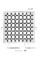
図7及び図8は実際の平面パターンを示す。図7に示す本発明の実施の形態に係る音響解析装置は、上面に凹部を備えた支持基板(図示省略)の上に構成されている。即ち、この支持基板の周辺部において、凹部を囲んで配置された固定枠12と、固定枠12に両端部を固定され、行方向及びこの行方向に直交する列方向にそれぞれ伸延し、凹部と固定枠12がなす空間に格子を構成するように配置された複数の配線梁21と、格子の窓部にそれぞれ配置され、音響入力によりそれぞれ振動し、振動子アレイを構成する複数の振動子Vi,j-1,Vi,j,Vi,j+1,・・・・・と、複数の振動子Vi,j-1,Vi,j,Vi,j+1,・・・・・のそれぞれと配線梁21とを接続する弾性梁22とを備えている。図7の水平方向(行方向)の配線梁21にはワード線が埋め込まれている。それぞれのワード線は、固定枠12の内部に形成されたワード線ドライバ(図示省略)に接続されている。又、図7の垂直方向(列方向)の配線梁21にはビット線が埋め込まれている。それぞれのビット線は、固定枠12の内部に形成されたビット線ドライバ(図示省略)及びセンスアンプ(図示省略)に接続されている。弾性梁22も、図10に示すようにドープドポリシリコン膜からなる配線層が含まれている。そして、この配線梁21と弾性梁22を介して複数の振動子Vi,j-1,Vi,j,Vi,j+1,・・・・・のそれぞれと固定枠12とは電気的に接続されている。
【0034】
そして、複数の振動子Vi,j-1,Vi,j,Vi,j+1,・・・・・のそれぞれと凹部の表面との間に印加する電圧により、複数の振動子Vi,j-1,Vi,j,Vi,j+1,・・・・・の共振周波数を変化させ、且つ複数の振動子のそれぞれが凹部の表面となす容量の変化により複数の振動子Vi,j-1,Vi,j,Vi,j+1,・・・・・のそれぞれの変位を検知し、この検知結果を用いて、音響入力のスペクトル解析を行い、インテリジェント・マイクロフォンとして機能する。
【0035】
このインテリジェント・マイクロフォンにおいては、センスアンプの出力が、図9に示したオペアンプ91に入力され、このオペアンプ91の出力電圧が基準電圧Vrefとコンパレータ92で比較される。したがって、固定枠12の内部にオペアンプ91及びコンパレータ92を集積化しても良い。
【0036】
図7では、配線梁21がなす格子の窓部にそれぞれ正方形の平面パターンの振動子Vi,j-1,Vi,j,Vi,j+1,・・・・・が配置されているが、振動子Vi,j-1,Vi,j,Vi,j+1,・・・・・の平面パターンは正方形に限定されるものではない。図7においては、それぞれの振動子Vi,j-1,Vi,j,Vi,j+1,・・・のパターンの四隅とこの四隅に対向する配線梁21の窓の四隅のそれぞれの間にドープドポリシリコンからなる弾性梁22で接続されている。つまり、それぞれ、4本の弾性梁22で各振動子Vi,j-1,Vi,j,Vi,j+1,・・・・・が配線梁21に対し懸架されている。格子状の配線梁21は配線機能と同時に弾性体としての機能も有するので、配線梁21と弾性梁22とで、図1に示した弾性梁13と等価な機能を実現している。即ち、配線梁21と弾性梁22との全体で図3及び図4に例示した振動モードを可能にしている。
【0037】
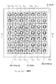
図8のパターンも図7のパターンと同様に、半導体基板の周辺部に設けられた固定枠12に格子状の配線梁21が設けられ、この配線梁21がなす格子の窓部にそれぞれ正方形の平面パターンの振動子Vi,j-1,Vi,j,Vi,j+1,・・・・・が配置されている。図8の水平方向(行方向)の配線梁21には、図7と同様に、ワード線が埋め込まれている。それぞれのワード線は、固定枠12の内部に形成されたワード線ドライバ(図示省略)に接続されている。又、図8の垂直方向(列方向)の配線梁21にはビット線が埋め込まれている。図8のC−C方向から見た断面図が、図10であり、図10の配線梁21にはメタル配線からなるビット線48が示されている。それぞれのビット線は、固定枠12の内部に形成されたビット線ドライバ(図示省略)及びセンスアンプ(図示省略)に接続されている。しかし、図8においては、周辺部の振動子・・・・・,Vi-3,j,・・・・・,Vi-2,j,・・・・・,Vi+ 2 ,j,・・・・・Vi+3,j,・・・・・のパターンの四辺とこの四辺に対向する配線梁21の窓の四辺のそれぞれの間は、折れ曲り箇所がなく直線状の第1弾性梁22aで接続され、中央部の振動子Vi-1,j-1,・・・・・,Vi,j-1,Vi,j,Vi,j+1,・・・・・,Vi+1,j,・・・・・のパターンの四辺とこの四辺に対向する配線梁21の窓の四辺のそれぞれの間は、2箇所で90°に折れ曲った第2弾性梁22bで接続されている。
【0038】
第1弾性梁22a及び第2弾性梁22bはそれぞれドープドポリシリコンから構成され、梁の長さ方向に垂直な断面形状も同じである。材料が同一であるので、第1弾性梁22a及び第2弾性梁22bのヤング率E及び密度ρは同じであるが、第1弾性梁22a及び第2弾性梁22bの長さLが異なるので、式(2)から明らかなように、第1弾性梁22a及び第2弾性梁22bのバネ定数kは互いに異なる値である。第1弾性梁22a、第2弾性梁22b及び配線梁21の全体で、図3及び図4に例示した振動モードを可能にしている。但し、図8に示す構造では中央部と周辺部の第1弾性梁22a及び第2弾性梁22bのバネ定数kが異なるように構成されているため、中央部と周辺部では共振周波数が異なる。マイクロフォンの感度を変化させることができ、周波数帯域(ダイナミックレンジ)を広げることが可能となっている。
【0039】
図8のC−C方向から見た断面図である図10においては、第2弾性梁22b中にドープドポリシリコン46が示されている。このドープドポリシリコン46は、図10の配線梁21において、メタル配線(ビット線)48の下層の配線としても存在する。図10の断面図には現れていないが、紙面の奥の配線梁21の内部でコンタクトホールを介して、上層のメタル配線(ビット線)48と下層のドープドポリシリコン配線46とは互いに接続されている。このため、ドープドポリシリコン46からなる配線は、それぞれの振動子・・・・・,Vi,j-1,Vi,j,Vi,j+1,・・・・・が検出した容量値を電圧信号として、メタル配線(ビット線)48に伝達することができる。
【0040】
図8のC−C方向から見た断面図である図11及び図12を用いて、図10に示す本発明の実施の形態に係る音響解析装置の製造方法を示す。なお、以下に述べる音響解析装置の製造方法は、一例であり、この変形例を含めて、これ以外の種々の製造方法により、実現可能であることは勿論である。
【0041】
(イ)まず、図11(a)に示すように、単結晶Siからなる半導体基板11上に埋め込み絶縁膜42、単結晶Si層からなる半導体層(SOI層)43が順次積層された、いわゆるSOI基板を準備する。半導体基板11は、比抵抗0,01Ω・cm〜0,02Ω・cmの低比抵抗のSi基板が好ましい。
【0042】
(ロ)次に、フォトリソグラフィー等の技術を用いて、図8に示す配線梁21,第1弾性梁22a及び第2弾性梁22bの形成予定領域の半導体層(SOI層)43を、例えばRIE等の技術により選択的にエッチング除去し、溝部を形成する。この溝部に酸化膜44をCVD法等の技術により埋め込み、化学的機械研磨(CMP)法等の技術で図11(b)に示すように平坦化する。
【0043】
(ハ)更に、半導体層(SOI層)43の表面にCVD法により、厚さ50nm〜100nmの第1層間絶縁膜45を形成する。次に、第1層間絶縁膜45の上の全面にCVD法によりポリシリコン膜46を300nm〜600nm程度、例えば400nm堆積する。次にフォトレジスト膜(以下において、単に「フォトレジスト」という。)をポリシリコン膜46の表面にスピン塗布する。そして、フォトリソグラフィー技術により、フォトレジストをパターニングする。そして、このフォトレジストをマスクとして、RIE法等によりポリシリコン膜46を図11(c)に示すようにエッチングする。そして、パターニングしたポリシリコン膜46にヒ素イオン(75As+)、燐イオン(31P+)或いは硼素イオン(11B+)等の不純物イオンをドーズ量1015cm−2のオーダーでイオン注入する。初めからこれらの不純物を添加したドープドポリシリコン膜46を第1層間絶縁膜45の上に堆積した後、図11(c)に示すようにエッチングしてパターニングしても良い。
【0044】
(ニ)次に図12に示すように、ポリシリコン膜46の表面にCVD法を用いて、第2層間絶縁膜47としてノンドープ酸化膜(NSG)、PSG膜、BSG膜、BPSG膜等の酸化膜を厚さ0.5μm〜1.0μm程度に形成する。そして、配線梁21形成予定のパターンの一部に、ポリシリコン膜46の一部を露出するコンタクトホールを開口する。コンタクトホールの開口は、フォトリソグラフィー技術とRIE法等によれば良い。そして、この第2層間絶縁膜47の上に、スパッタリング法又は電子ビーム真空蒸着法等によりチタン(Ti)、タングステン(W)等からなる金属膜を堆積する。金属膜は、配線梁21形成予定のパターンの一部に開口されたコンタクトホールの内部にも埋め込まれる。その後、フォトリソグラフィー技術等を用いたメタライゼーション技術により、金属膜をパターニングすれば、図12(a)に示すようなメタル配線48が形成される。メタル配線48は、図7及び図8に示した配線梁21に埋め込まれるワード線及びビット線を構成するが、メタル配線48とこの下層のポリシリコン膜46の配線とは、コンタクトホールを介して接続される。更に、メタル配線48及び第2層間絶縁膜47の上に、CVD法を用いて厚さ1.0μm程度のパッシベーション膜49を形成する。パッシベーション膜49としては、PSG膜、BSG膜、BPSG膜、若しくは窒化膜、或いはこれらの複合膜等を使用しても良い。そして、CMP法等を用いて図12(a)に示すように平坦化する。
【0045】
(ホ)更に、フォトリソグラフィー技術及びRIE法若しくはECRイオンエッチング法等で溝部51を形成し、図12(b)に示すように、配線梁21、第1弾性梁22a及び第2弾性梁22bを分離する。
【0046】
(ヘ)その後、このエッチングで露出した半導体基板11の表面の一部を、引き続き、単結晶Siの異方性エッチャント、例えばテトラメチルアンモニウムハイドロオキサイド(TMAH)等の薬液を用いて、異方性エッチングを行えば、図10に示すような各振動子Vi,j-1,Vi,j,Vi,j+1,・・・・・が配線梁21に対し懸架された構造ができる。更に、半導体基板11の裏面にCVD法で酸化膜を堆積し、フォトリソグラフィー技術を用いてドライ又はウエットで酸化膜をエッチングした後、この酸化膜をマスクとして、TMAHなどで半導体基板11を異方性エッチングすることで裏面溝52が形成され、図10に示した本発明の実施の形態に係る音響解析装置が完成する。
【0047】
(その他の実施の形態)
上記のように、本発明は上記の実施の形態によって記載したが、この開示の一部をなす論述及び図面はこの発明を限定するものであると理解すべきではない。この開示から当業者には様々な代替実施の形態、実施例及び運用技術が明らかとなろう。
【0048】
例えば、図7で説明した実施の形態の説明においては、配線梁21が弾性体として機能し、配線梁21と弾性梁22との全体で図3及び図4に例示した振動モードを可能にする場合を説明したが、行方向の配線梁21の剛性を強くし、固定梁として機能させても良い。この場合、行方向に各振動子Vi,j-1,Vi,j,Vi,j+1,・・・・・が弾性梁を介して相互に結合し、これにより振動子チェーン(振動子鎖)を構成し、各行毎に異なる共振周波数の振動子チェーンになるように弾性梁22のバネ定数若しくは、振動子の質量を異なるようにすれば、極めて広帯域の音響解析装置が提供できる。
【0049】
又、半導体基板11a,11b,11cを、低比抵抗のSi基板とし、それぞれのコンデンサCi,j-1,Ci,j,Ci,j+1,・・・・・に共通の電極となる例を示したが、半導体基板11a,11b,11c側に、各行に独立したメタル配線等の配線層を設け、各行毎に異なる電位を与え、各行をそれぞれ独立に共振周波数を制御可能なようにして、共振周波数制御手段を構成し、音響解析装置に学習可能な機能を付与させても良い。
【0050】
或いは、列方向の配線梁21の剛性を強くし、固定梁として機能させ、列方向に各振動子Vi,j-1,Vi,j,Vi,j+1,・・・・・が弾性梁を介して相互に結合し、これにより振動子チェーンを構成し、各列毎に異なる共振周波数の振動子チェーンになるように弾性梁22のバネ定数若しくは、振動子の質量を異なるようにしても良い。更に、半導体基板11a,11b,11c側に、各列に独立した配線層を設け、各列毎に異なる電位を与え、各列をそれぞれ独立に共振周波数を制御可能なように共振周波数制御手段を構成しても良い。
【0051】
更に、行方向及び列方向の配線梁21をともに固定梁として機能させ、各振動子Vi,j-1,Vi,j,Vi,j+1,・・・・・を独立に振動させる振動モードも可能である。そして、2次元マトリクスとして配列された個々の振動子Vi,j-1,Vi,j,Vi,j+1,・・・・・の共振周波数をすべて異なるようにし、或いは、個々の振動子Vi,j-1,Vi,j,Vi,j+1,・・・・・の共振周波数をすべて独立に制御するように共振周波数制御手段を構成し、振動させても良い。
【0052】
このように、本発明はここでは記載していない様々な実施の形態等を含むことは勿論である。したがって、本発明の技術的範囲は上記の説明から妥当な特許請求の範囲に係る発明特定事項によってのみ定められるものである。
【0053】
【発明の効果】
本発明によれば、音響入力に対してそれぞれの振動子の振幅及び位相情報が得られ、周波数毎の振幅が解析でき、ノイズの除去が容易になる。この結果、音声入力の場合は、特定の話者に応じたスペクトルが得られて、音声認識率が改善された音響解析装置を提供できる。
【0054】
更に、本発明によれば、ノイズのある場所においても、特別な学習をさせることなく、不特定多数の会話を認識できる音響解析装置を提供できる。
【図面の簡単な説明】
【図1】本発明の実施の形態に係る音響解析装置の振動子アレイの模式的な平面パターンである。
【図2】図1のA−A方向から見た模式的断面図である。
【図3】基本波モード(基本周波数f1)における本発明の実施の形態に係る音響解析装置の振動子アレイの振動モードを示す模式的断面図である。
【図4】第2高調波(周波数f2)における本発明の実施の形態に係る音響解析装置の振動子アレイの振動モードを示す模式的断面図である。
【図5】本発明の実施の形態の変形例に係る音響解析装置の振動子アレイの模式的断面図である。
【図6】本発明の実施の形態の他の変形例に係る音響解析装置の振動子アレイの模式的断面図である。
【図7】本発明の実施の形態に係る音響解析装置の振動子アレイの具体的構造を示す平面パターンである。
【図8】本発明の実施の形態に係る音響解析装置の振動子アレイの他の具体的構造を示す平面パターンである。
【図9】本発明の実施の形態に係る音響解析装置の検出回路の一例を示す回路図である。
【図10】本発明の実施の形態の変形例に係る音響解析装置の振動子アレイの具体的な断面図である。
【図11】図10に示した振動子アレイの製造方法を説明する工程断面図である(その1)。
【図12】図10に示した振動子アレイの製造方法を説明する工程断面図である(その2)。
【図13】従来の音声認識方法を説明するフローチャートである。
【図14】従来の音声分析システムを説明するブロック図である。
【図15】従来の周波数分析用メカニカル・フィルタの構造を説明する平面図である。
【符号の説明】
11,11a,11b,11c…半導体基板
12…固定枠
13,22…弾性梁
21…配線梁
22a…第1弾性梁
22b…第2弾性梁
42…絶縁膜
43…半導体層
44…酸化膜
45…第1層間絶縁膜
46…ポリシリコン膜(ドープドポリシリコン膜)
47…第2層間絶縁膜
48…メタル配線
49…パッシベーション膜
51…溝部
52…裏面溝
91…オペアンプ
92…コンパレータ
101…Si基板
104…標準パターン
111…終端
112…ダイアフラム
115…横梁
201…マイクロフォン
203…コンバータ
204…FFT装置
C0…可変容量コンデンサ
C1…コンデンサ
Vbias…電源電圧
Vi,j-1,Vi,j,Vi,j+1,・・・・・…振動子
Vref…基準電圧[0001]
BACKGROUND OF THE INVENTION
The present invention relates to an acoustoelectric transducer, and more particularly to an acoustic analyzer that analyzes an acoustic spectrum using the acoustoelectric transducer.
[0002]
[Prior art]
The speech recognition technology is very good as an interface between a computer and a machine and a human. However, the ease of recognition differs depending on the speaker, vocabulary, and utterance factors, and it is affected by ambient noise. For this reason, in order to improve the recognition rate, the speaker to be recognized needs to learn the computer in advance, and it is difficult to recognize an unspecified number of conversations. For this reason, there is a need for a speech analysis technique that is as accurate as possible.
[0003]
In the standard speech recognition method, as shown in FIG. 13, first, features of the input speech signal are extracted by speech analysis in step S101. Then, after normalization with respect to the time axis in step S102, similarity is determined in step S103 by comparison with the
[0004]
As shown in FIG. 14, in a general voice analysis system, a
[0005]
By the way, the sound wave incident on the human eardrum is transmitted to the cochlea through the ear ossicles. The cochlea is separated into two areas by the base plate, and the pressure difference that occurs in these two areas is detected as sound. Is different. Furthermore, recent research has shown that frequency discrimination and selection can be achieved by a feedback mechanism in which the vibration of the basement plate is amplified by the action of outer hair cells (OHC) in the cochlea (Non-patent Document 1). reference.).
[0006]
As an example simulating this cochlea, a frequency analysis mechanical filter as shown in FIG. 15 has been proposed (see Patent Document 1). In FIG. 15, the sound wave incident on the diaphragm 112 provided on the surface of the
[0007]
[Patent Document 1]
US Pat. No. 6,079,274
[0008]
[Non-Patent Document 1]
Journal of the Acoustical Society of Japan, Vol. 59, No. 1, 2003, p. 40-45
[0009]
[Problems to be solved by the invention]
However, the frequency analysis mechanical filter shown in FIG. 15 has a problem that sensitivity is lowered because only a part of the incident sound wave energy is transmitted to the vibrator (resonator beam) 113.
[0010]
Furthermore, the conventional speech recognition technology requires a learning process for each user, and can be used only in a place with low noise, which causes a problem in usability.
In view of the above problems, the present invention provides an acoustic analysis apparatus capable of obtaining the amplitude and phase information of each transducer with respect to an acoustic input such as a voice input and thereby directly analyzing the frequency of the acoustic signal. The purpose is to provide.
[0011]
Another object of the present invention is to provide an acoustic analysis device that can easily remove noise.
[0012]
In particular, in the case of voice input, an object is to provide an acoustic analysis device in which a spectrum corresponding to a specific speaker is obtained and the voice recognition rate is improved. It is another object of the present invention to provide an acoustic analysis apparatus that can recognize an unspecified number of conversations in a noisy place without special learning.
[0013]
[Means for Solving the Problems]
In order to achieve the above object, the first feature of the present invention is that (a) a transducer array composed of a plurality of transducers that vibrate in response to an acoustic input, and An elastic beam; (c) a displacement detection means for detecting the displacement of the vibrator; and (d) a resonance frequency control means for changing the resonance frequency of the vibrator array. The gist of the present invention is that it is an acoustic analysis device that performs analysis.
[0014]
According to the first feature of the present invention, amplitude and phase information of each vibrator can be obtained for an acoustic input such as a voice input. For this reason, the amplitude for each frequency can be analyzed, noise can be easily removed, and in the case of voice input, a spectrum corresponding to a specific speaker is obtained, and the voice recognition rate is improved. In particular, when the transducer array has a structure similar to that of a human ear, it is possible to directly analyze the frequency of an audio signal and recognize an unspecified number of conversations without special learning.
The second feature of the present invention is that (a) a support substrate having a recess on the upper surface, (b) a fixing frame disposed around the recess at the periphery of the support substrate, and (c) fixing the recess A plurality of transducers that are arranged to form a transducer array in a space formed by the frame and vibrate by acoustic input, and (d) an end transducer that is closest to the fixed frame among the plurality of transducers; An elastic beam that connects the fixed frame and connects the end vibrator and the other vibrator to each other, and the vibrator applies a voltage applied between each of the vibrators and the surface of the recess. The resonance frequency of the array is changed, and the displacement of each of the plurality of transducers is detected by the change in the capacitance of each of the plurality of transducers with the surface of the recess. Using this detection result, the spectrum analysis of the acoustic input is performed. The gist is that it is an acoustic analysis device to be performed.
[0015]
According to the second feature of the present invention, similarly to the first feature, amplitude and phase information of each transducer can be obtained for an acoustic input. For this reason, the amplitude for each frequency can be analyzed, noise can be easily removed, and when the sound input is speech, a spectrum corresponding to a specific speaker is obtained, and the speech recognition rate is improved. In particular, by making the transducer array similar to the human ear using micromachine technology, it is possible to perform frequency analysis directly on the audio signal, and without any special learning, many unspecified conversations. Can be recognized.
[0016]
The third feature of the present invention is that (a) a support substrate having a recess on its upper surface, (b) a fixed frame disposed around the recess at the periphery of the support substrate, and (c) a fixed frame A plurality of wiring beams fixed at both ends, extending in the row direction and the column direction perpendicular to the row direction, and arranged to form a lattice in the space formed by the recess and the fixed frame; A plurality of vibrators that are respectively arranged in the window portion and vibrate by acoustic input and constitute a vibrator array; and (e) an elastic beam that connects each of the plurality of vibrators and the wiring beam, The resonance frequency of the plurality of vibrators is changed by the voltage applied between each of the vibrators and the surface of the recess, and the change of the capacitance that each of the vibrators forms the surface of the recesses changes Detect each displacement and use this detection result And summarized in that an acoustic analyzer for performing spectral analysis of the acoustic input.
[0017]
According to the third feature of the present invention, similarly to the first and second features, amplitude and phase information of each transducer can be obtained with respect to an acoustic input. For this reason, the amplitude for each frequency can be analyzed, noise can be easily removed, and in the case of voice input, a spectrum corresponding to a specific speaker is obtained, and the voice recognition rate is improved. In particular, by using a micromachine technology to make the transducer array similar in structure to the human ear, it is possible to directly analyze the frequency of the audio signal, without any special learning Can recognize conversations.
[0018]
DETAILED DESCRIPTION OF THE INVENTION
Next, embodiments of the present invention will be described with reference to the drawings. In the following description of the drawings, the same or similar parts are denoted by the same or similar reference numerals. However, it should be noted that the drawings are schematic, and the relationship between the thickness and the planar dimensions, the ratio of the thickness of each layer, and the like are different from the actual ones. Therefore, specific thicknesses and dimensions should be determined in consideration of the following description. Moreover, it is a matter of course that portions having different dimensional relationships and ratios are included between the drawings.
[0019]
Further, the following embodiments exemplify apparatuses and methods for embodying the technical idea of the present invention, and the technical idea of the present invention is the material, shape, structure, The layout is not specified as follows. The technical idea of the present invention can be variously modified within the scope of the claims.
[0020]
As shown in the plane pattern of FIG. 1, the acoustic analysis device according to the embodiment of the present invention is disposed so as to surround the concave portion in the
[0021]
Here, the
[0022]
FIG. 2 is a cross-sectional view seen from the AA direction in FIG. 1 and shows each vibrator V created on the SOI substrate.i, j-1, Vi, j, Vi, j + 1, V, Vi, j-1, Vi, j, Vi, j + 1,... Indicate specific rows of the transducer array connected to each other by the elastic beam 13 (a more detailed cross-sectional structure is shown in FIG. 10). A specific row of the transducer array apparently constitutes a one-dimensional transducer chain (oscillator chain), but in reality, it is a two-dimensional transducer array as shown in FIG. Each transducer V constituting the transducer arrayi, j-1, Vi, j, Vi, j + 1,... Partially include a
[0023]
Each vibrator V constituting the acoustic analysis apparatus according to the embodiment of the present inventioni, j-1, Vi, j, Vi, j + 1, ... mass is about 10-12The spring constant k of the
[0024]
In the case of an N transducer array, the primary transverse natural frequency (fundamental frequency) f1Is the vibrator Vi, j-1, Vi, j, Vi, j + 1, ... mass m and vibrator Vi, j-1, Vi, j, Vi, j + 1, ... are connected to the spring constant k [N / m of the elastic beam 132] By:
f1= 1 / 2π × (k / m)1/2 (1)
It is expressed. here,
k = EhwThree/ LThree (2)
m = Stρ (3)
Where L, h and w are the length [m], thickness [m] and width [m] of the
[0025]
In the acoustic analysis apparatus according to the embodiment of the present invention, the support substrate (semiconductor substrate) 11a and the vibrator Vi, j-1, Vi, j, Vi, j + 1When a voltage Ψ is applied between the vibrator V and the vibrator V due to electrostatic forcei, j-1, Vi, j, Vi, j + 1,... Are displaced, so that the vibrator Vi, j-1, Vi, j, Vi, j + 1The spring constant k of the
Δk = ε × S / d3× Ψ2 (4)
The first-order natural frequency (fundamental frequency) f of the transducer array1Can be changed. Here, ε and d are the dielectric constant of air and the support substrate (semiconductor substrate) 11a and the vibrator V.i, j-1, Vi, j, Vi, j + 1,... In other words, the “resonance frequency control means” of the acoustic analysis device according to the embodiment of the present invention thus uses the vibrator V by electrostatic force.i, j-1, Vi, j, Vi, j + 1Are displaced to change the resonance frequency of the transducer array.
[0026]
When sound is further input in this state, each transducer Vi, j-1, Vi, j, Vi, j + 1... Are displaced with respect to the voice input direction. For example, the fundamental frequency F of a specific speaker's voice1To the primary natural frequency f of the transducer array1If the voice of the specific speaker is input to the acoustic analysis apparatus according to the embodiment of the present invention, a spectrum responding with high sensitivity to the voice input can be obtained.
[0027]
As shown in FIGS. 3A and 3B, the transverse wave vibration mode of the one-dimensional vibrator chain (vibrator chain) composed of seven vibrators is the fundamental wave mode (fundamental frequency f).1), The central vibrator V so that the central portion becomes antinode according to the sound pressure.i, jThe displacement of is large.
[0028]
On the other hand, the frequency f2In the case of the second harmonic, the one-dimensional vibrator chain is in a transverse wave vibration mode as shown in FIG. In FIG. 4, the central vibrator V constituting the vibrator chaini, jBecomes a node and its displacement is zero, but the left vibrator Vi, j-1, Vi, j-2And right vibrator Vi, j + 1, Vi, j + 2The displacement of is large. Although not shown, the frequency fThreeIn the case of the third harmonic of the oscillator V in the center of the oscillator chaini, jThe displacement of the left vibrator Vi, j-2And right vibrator Vi, j + 2Becomes a node, and its displacement is zero. And the left vibrator Vi, j-3, Vi, j-1And right vibrator Vi, j + 1, Vi, j + 3The displacement of increases.
[0029]
In general, the speech waveform has a fundamental frequency F1, Second harmonic frequency F2, 3rd harmonic frequency FThree,... Are superimposed on each eigenmode. For this reason, each vibrator Vi, j-1, Vi, j, Vi, j + 1,... Have eigenmode amplitude and phase information.
[0030]
FIG. 9 shows an example of a “displacement detection unit” that detects the displacement of the vibrator of the acoustic analysis apparatus according to the embodiment of the present invention, that is, a detection circuit. In FIG. 9, each vibrator V shown in FIG.i, j-1, Vi, j, Vi, j + 1, ... and the capacitance C between the support substrate (semiconductor substrate) 11ai, j-1, Ci, j, Ci, j + 1, ... variable capacitor C0This is shown as a representative. Variable capacitor C0There is a power supply voltage VbiasIs applied. Variable capacitor C0Is input to the inverting input terminal of the
[0031]
Vibrator Vi, j-1, Vi, j, Vi, j + 1, ... and the capacitance C between the support substrate (semiconductor substrate) 11ai, j-1, Ci, j, Ci, j + 1, ... are the vibrator Vi, j-1, Vi, j, Vi, j + 1, ... and the distance between the support substrate (semiconductor substrate) 11a is Δdi, jΔdi, jAre sufficiently small, respectively:
ΔCi, j= Ε × S / Δdi, j (5)
It can be approximated by fluctuation. Each vibrator Vi, j-1, Vi, j, Vi, j + 1,... Are wired through a doped polysilicon spring (elastic beam) 13. For this reason, the vibrator Vi, j-1, Vi, j, Vi, j + 1...,. Capacitance Ci, j-1, Ci, j, Ci, j + 1When the switch SW1 connected in parallel with the capacitor SW is opened, the capacitance Ci, j-1, Ci, j, Ci, j + 1,... Are time integrated with the
[0032]
In FIG. 2, since etching is performed only from the front surface, there is no hole for penetrating the silicon substrate as the
[0033]
7 and 8 show actual planar patterns. The acoustic analysis apparatus according to the embodiment of the present invention shown in FIG. 7 is configured on a support substrate (not shown) having a recess on the upper surface. That is, at the periphery of the support substrate, the fixed
[0034]
And a plurality of vibrators Vi, j-1, Vi, j, Vi, j + 1,... And a voltage applied between the surfaces of the recesses, so that a plurality of vibrators Vi, j-1, Vi, j, Vi, j + 1,... Are changed, and the plurality of vibrators V are changed by the change in capacitance that each of the plurality of vibrators forms with the surface of the recess.i, j-1, Vi, j, Vi, j + 1...,... Are detected, and a spectrum analysis of the acoustic input is performed using the detection result, thereby functioning as an intelligent microphone.
[0035]
In this intelligent microphone, the output of the sense amplifier is input to the
[0036]
In FIG. 7, the vibrator V having a square plane pattern is formed in each of the lattice windows formed by the wiring beams 21.i, j-1, Vi, j, Vi, j + 1Are arranged, but the vibrator Vi, j-1, Vi, j, Vi, j + 1The planar pattern is not limited to a square. In FIG. 7, each vibrator Vi, j-1, Vi, j, Vi, j + 1,... Are connected by elastic beams 22 made of doped polysilicon between the four corners of the pattern and the four corners of the window of the
[0037]
Similarly to the pattern of FIG. 7, the pattern of FIG. 8 is also provided with a grid-
[0038]
The first elastic beam 22a and the second
[0039]
In FIG. 10, which is a cross-sectional view seen from the CC direction of FIG. 8, doped
[0040]
A manufacturing method of the acoustic analysis device according to the embodiment of the present invention shown in FIG. 10 will be described with reference to FIGS. 11 and 12 which are cross-sectional views seen from the CC direction of FIG. Note that the method for manufacturing the acoustic analysis device described below is an example, and it is needless to say that the method can be realized by various other manufacturing methods including this modification.
[0041]
(A) First, as shown in FIG. 11A, a buried insulating
[0042]
(B) Next, using a technique such as photolithography, the semiconductor layer (SOI layer) 43 in a region where the
[0043]
(C) Further, a first
[0044]
(D) Next, as shown in FIG. 12, a CVD method is used on the surface of the
[0045]
(E) Further, the
[0046]
(F) Thereafter, a part of the surface of the
[0047]
(Other embodiments)
As described above, the present invention has been described according to the above-described embodiments. However, it should not be understood that the description and drawings constituting a part of this disclosure limit the present invention. From this disclosure, various alternative embodiments, examples, and operational techniques will be apparent to those skilled in the art.
[0048]
For example, in the description of the embodiment described with reference to FIG. 7, the
[0049]
Further, the
[0050]
Alternatively, the rigidity of the
[0051]
Further, the wiring beams 21 in the row direction and the column direction are both functioned as fixed beams, and each vibrator Vi, j-1, Vi, j, Vi, j + 1A vibration mode that vibrates independently is also possible. The individual vibrators V arranged as a two-dimensional matrixi, j-1, Vi, j, Vi, j + 1,... Are all made different from each other, or individual vibrators Vi, j-1, Vi, j, Vi, j + 1The resonance frequency control means may be configured to vibrate so that all the resonance frequencies of.
[0052]
As described above, the present invention naturally includes various embodiments not described herein. Therefore, the technical scope of the present invention is defined only by the invention specifying matters according to the scope of claims reasonable from the above description.
[0053]
【The invention's effect】
According to the present invention, amplitude and phase information of each vibrator can be obtained with respect to an acoustic input, the amplitude for each frequency can be analyzed, and noise can be easily removed. As a result, in the case of voice input, a spectrum corresponding to a specific speaker can be obtained, and an acoustic analysis device with improved voice recognition rate can be provided.
[0054]
Furthermore, according to the present invention, it is possible to provide an acoustic analysis apparatus that can recognize an unspecified number of conversations in a noisy place without special learning.
[Brief description of the drawings]
FIG. 1 is a schematic plane pattern of a transducer array of an acoustic analysis device according to an embodiment of the present invention.
FIG. 2 is a schematic cross-sectional view as seen from the AA direction in FIG.
FIG. 3 shows a fundamental wave mode (
FIG. 4 shows the second harmonic (
FIG. 5 is a schematic cross-sectional view of a transducer array of an acoustic analysis device according to a modification of the embodiment of the present invention.
FIG. 6 is a schematic cross-sectional view of a transducer array of an acoustic analysis device according to another modification of the embodiment of the present invention.
FIG. 7 is a plan pattern showing a specific structure of the transducer array of the acoustic analysis device according to the embodiment of the present invention.
FIG. 8 is a plan pattern showing another specific structure of the transducer array of the acoustic analysis device according to the embodiment of the present invention.
FIG. 9 is a circuit diagram illustrating an example of a detection circuit of the acoustic analysis device according to the embodiment of the present invention.
FIG. 10 is a specific cross-sectional view of a transducer array of an acoustic analysis device according to a modification of the embodiment of the present invention.
FIG. 11 is a process cross-sectional view illustrating the manufacturing method of the transducer array shown in FIG. 10 (No. 1);
12 is a process cross-sectional view illustrating the manufacturing method of the transducer array shown in FIG. 10 (part 2);
FIG. 13 is a flowchart illustrating a conventional speech recognition method.
FIG. 14 is a block diagram illustrating a conventional speech analysis system.
FIG. 15 is a plan view illustrating the structure of a conventional frequency analysis mechanical filter.
[Explanation of symbols]
11, 11a, 11b, 11c ... Semiconductor substrate
12 ... Fixed frame
13, 22 ... Elastic beam
21 ... Wiring beams
22a ... 1st elastic beam
22b ... second elastic beam
42. Insulating film
43 ... Semiconductor layer
44 ... Oxide film
45. First interlayer insulating film
46. Polysilicon film (doped polysilicon film)
47. Second interlayer insulating film
48 ... Metal wiring
49 ... Passivation film
51 ... Groove
52 ... Back groove
91. Operational amplifier
92 ... Comparator
101 ... Si substrate
104 ... Standard pattern
111 ... Termination
112 ... Diaphragm
115 ... Horizontal beam
201: Microphone
203 ... Converter
204 ... FFT device
C0... Variable capacitor
C1... Capacitor
Vbias…Power-supply voltage
Vi, j-1, Vi, j, Vi, j + 1, ... vibrator
Vref... reference voltage
Claims (13)
振動子チェーンを構成するように、前記複数の振動子の相互間を順に行方向に接続する複数の弾性梁と、
前記振動子の変位を検知する変位検知手段と、
静電気力により、前記複数の弾性梁のバネ定数を変化させ、前記振動子チェーンの共振周波数を変化させる共振周波数制御手段
とを備え、前記変位検知手段の出力により、前記音響入力のスペクトル解析を行うことを特徴とする音響解析装置。 A plurality of vibrators that vibrate in response to acoustic inputs and have the same mass ,
A plurality of elastic beams for connecting the plurality of vibrators in a row direction in order to form a vibrator chain ;
Displacement detecting means for detecting the displacement of the vibrator;
Resonance frequency control means for changing the spring constant of the plurality of elastic beams by electrostatic force and changing the resonance frequency of the vibrator chain , and performing spectrum analysis of the acoustic input by the output of the displacement detection means An acoustic analysis device characterized by that.
該支持基板の周辺部において、前記凹部を囲んで配置された固定枠と、
前記凹部と前記固定枠がなす空間に、振動子チェーンの一部をなすように配置され、音響入力によりそれぞれ振動し、それぞれ同一質量を有した複数の振動子と、
前記複数の振動子のうち前記固定枠に最近接となる端部振動子と前記固定枠とを接続し、且つ該端部振動子と他の振動子とを相互間を順に行方向に接続し、前記振動子チェーンを構成する複数の弾性梁
とを備え、前記複数の振動子のそれぞれと前記凹部の表面との間に印加する電圧により、前記複数の弾性梁のバネ定数を変化させ、前記振動子チェーンの共振周波数を変化させ、且つ前記複数の振動子のそれぞれが前記凹部の表面となす容量の変化により前記複数の振動子のそれぞれの変位を検知し、該検知結果を用いて、前記音響入力のスペクトル解析を行うことを特徴とする音響解析装置。A support substrate having a recess on the upper surface;
A fixing frame disposed around the concave portion in the periphery of the support substrate;
A plurality of vibrators arranged in a space formed by the concave portion and the fixed frame so as to form a part of a vibrator chain, respectively oscillating by acoustic input, and having the same mass ;
The end vibrator that is closest to the fixed frame and the fixed frame of the plurality of vibrators are connected to the fixed frame, and the end vibrator and the other vibrators are sequentially connected to each other in the row direction. A plurality of elastic beams constituting the vibrator chain, and a spring constant of the plurality of elastic beams is changed by a voltage applied between each of the plurality of vibrators and the surface of the recess , The resonance frequency of the vibrator chain is changed, and the displacement of each of the plurality of vibrators is detected by the change in capacitance of each of the plurality of vibrators with the surface of the recess, and the detection result is used to An acoustic analysis apparatus characterized by performing spectrum analysis of acoustic input.
該支持基板の周辺部において、前記凹部を囲んで配置された固定枠と、
前記固定枠に両端部を固定され、行方向及び該行方向に直交する列方向にそれぞれ伸延し、前記凹部と前記固定枠がなす空間に格子を構成するように配置された複数の配線梁と、
前記格子の窓部にそれぞれ配置され、音響入力によりそれぞれ振動し、振動子アレイの一部を構成する複数の振動子と、
前記複数の振動子のそれぞれと前記配線梁とを接続する弾性梁
とを備え、前記複数の振動子のそれぞれと前記凹部の表面との間に印加する電圧により、前記複数の振動子の共振周波数を変化させ、且つ前記複数の振動子のそれぞれが前記凹部の表面となす容量の変化により前記複数の振動子のそれぞれの変位を検知し、該検知結果を用いて、前記音響入力のスペクトル解析を行うことを特徴とする音響解析装置。A support substrate having a recess on the upper surface;
A fixing frame disposed around the concave portion in the periphery of the support substrate;
A plurality of wiring beams fixed at both ends to the fixed frame, extending in a row direction and a column direction orthogonal to the row direction, and arranged so as to form a lattice in a space formed by the concave portion and the fixed frame; ,
A plurality of vibrators that are respectively disposed in the window portions of the lattice, vibrate by acoustic input, and constitute a part of the vibrator array;
An elastic beam connecting each of the plurality of vibrators and the wiring beam, and a resonance frequency of the plurality of vibrators by a voltage applied between each of the plurality of vibrators and the surface of the recess. And the displacement of each of the plurality of transducers is detected by a change in the capacitance of each of the plurality of transducers with the surface of the recess, and the spectrum analysis of the acoustic input is performed using the detection result. An acoustic analysis apparatus characterized by performing.
前記振動子チェーンの一部に用いられる第1弾性梁と、
前記振動子チェーンの他の一部に用いられ、且つ前記第1弾性梁とはバネ定数が異なる第2弾性梁
とを含むことを特徴とする請求項1に記載の音響解析装置。The elastic beam is
A first elastic beam used in a part of the vibrator chain ;
The acoustic analysis apparatus according to claim 1 , further comprising: a second elastic beam that is used in another part of the vibrator chain and has a spring constant different from that of the first elastic beam.
前記振動子チェーンの一部に用いられる第1弾性梁と、
前記振動子チェーンの他の一部に用いられ、且つ前記第1弾性梁とはバネ定数が異なる第2弾性梁
とを含むことを特徴とする請求項2又は3のいずれか1項に記載の音響解析装置。The elastic beam is
A first elastic beam used in a part of the vibrator chain ;
4. The second elastic beam according to claim 2 , further comprising: a second elastic beam that is used in another part of the vibrator chain and has a spring constant different from that of the first elastic beam. 5. Acoustic analysis device.
前記振動子アレイの一部に用いられる第1弾性梁と、
前記振動子アレイの他の一部に用いられ、且つ前記第1弾性梁とはバネ定数が異なる第2弾性梁
とを含むことを特徴とする請求項4〜6のいずれか1項に記載の音響解析装置。The elastic beam is
A first elastic beam used in a part of the transducer array;
7. The second elastic beam according to claim 4 , further comprising: a second elastic beam that is used in another part of the transducer array and has a spring constant different from that of the first elastic beam. Acoustic analysis device.
該オペアンプの出力と基準電圧とを比較するコンパレータ
とを更に備えることを特徴とする請求項2〜10のいずれか1項に記載の音響解析装置。The acoustic analysis according to any one of claims 2 to 10 , further comprising: an operational amplifier that inputs a change in voltage caused by the change in capacitance, and a comparator that compares an output of the operational amplifier with a reference voltage. apparatus.
Priority Applications (1)
| Application Number | Priority Date | Filing Date | Title |
|---|---|---|---|
| JP2003200057A JP3802014B2 (en) | 2003-07-22 | 2003-07-22 | Acoustic analyzer |
Applications Claiming Priority (1)
| Application Number | Priority Date | Filing Date | Title |
|---|---|---|---|
| JP2003200057A JP3802014B2 (en) | 2003-07-22 | 2003-07-22 | Acoustic analyzer |
Publications (2)
| Publication Number | Publication Date |
|---|---|
| JP2005043073A JP2005043073A (en) | 2005-02-17 |
| JP3802014B2 true JP3802014B2 (en) | 2006-07-26 |
Family
ID=34260627
Family Applications (1)
| Application Number | Title | Priority Date | Filing Date |
|---|---|---|---|
| JP2003200057A Expired - Fee Related JP3802014B2 (en) | 2003-07-22 | 2003-07-22 | Acoustic analyzer |
Country Status (1)
| Country | Link |
|---|---|
| JP (1) | JP3802014B2 (en) |
Families Citing this family (3)
| Publication number | Priority date | Publication date | Assignee | Title |
|---|---|---|---|---|
| JP4552883B2 (en) * | 2006-04-19 | 2010-09-29 | 株式会社デンソー | Vibration detection method |
| JP6961638B2 (en) * | 2019-03-14 | 2021-11-05 | 株式会社東芝 | Sensor module |
| JP7005545B2 (en) * | 2019-03-15 | 2022-02-10 | 株式会社東芝 | Sensor module |
-
2003
- 2003-07-22 JP JP2003200057A patent/JP3802014B2/en not_active Expired - Fee Related
Also Published As
| Publication number | Publication date |
|---|---|
| JP2005043073A (en) | 2005-02-17 |
Similar Documents
| Publication | Publication Date | Title |
|---|---|---|
| US10506345B2 (en) | System and method for a microphone | |
| CN107872760B (en) | MEMS device | |
| EP0852708B1 (en) | Mechanical signal processor based on micromechanical oscillators and intelligent acoustic detectors and systems based thereon | |
| KR101807146B1 (en) | High sensitivity microphone and manufacturing method thereof | |
| US7907744B2 (en) | Capacitive vibration sensor and method for manufacturing same | |
| US7146014B2 (en) | MEMS directional sensor system | |
| US8989411B2 (en) | Differential microphone with sealed backside cavities and diaphragms coupled to a rocking structure thereby providing resistance to deflection under atmospheric pressure and providing a directional response to sound pressure | |
| JP6830527B2 (en) | Piezoelectric Microphone Chips and Piezoelectric Microphones | |
| KR20160020287A (en) | Audio sensing device and method of acquiring frequency information | |
| US20120091546A1 (en) | Microphone | |
| KR101360104B1 (en) | Surface micromachined differential microphone | |
| KR101550636B1 (en) | Micro phone and method manufacturing the same | |
| KR20090071648A (en) | Miniature non-directional microphone | |
| KR102212575B1 (en) | Microphone and manufacturing method thereof | |
| US10469958B2 (en) | MEMS sound transducer, MEMS microphone and method for providing a MEMS sound transducer | |
| JP2005110204A (en) | Capacitor microphone and its manufacturing method | |
| JP4244232B2 (en) | Condenser microphone and manufacturing method thereof | |
| JP3802014B2 (en) | Acoustic analyzer | |
| JP2008252847A (en) | Electrostatic transducer | |
| JP2008252854A (en) | Electrostatic transducer and manufacturing method thereof | |
| JP5022198B2 (en) | Method for manufacturing transducer substrate | |
| JP3884444B2 (en) | Acoustoelectric conversion system | |
| Huang et al. | Micromachined piezoelectric microphone with high signal to noise ratio | |
| JP2004085419A (en) | Resonator, resonator array, and acoustical sensor | |
| KR20040091207A (en) | Piezoelectric acoustic transducer and manufacturing method thereof |
Legal Events
| Date | Code | Title | Description |
|---|---|---|---|
| A977 | Report on retrieval |
Free format text: JAPANESE INTERMEDIATE CODE: A971007 Effective date: 20051226 |
|
| A131 | Notification of reasons for refusal |
Free format text: JAPANESE INTERMEDIATE CODE: A131 Effective date: 20060117 |
|
| A521 | Request for written amendment filed |
Free format text: JAPANESE INTERMEDIATE CODE: A523 Effective date: 20060317 |
|
| TRDD | Decision of grant or rejection written | ||
| A01 | Written decision to grant a patent or to grant a registration (utility model) |
Free format text: JAPANESE INTERMEDIATE CODE: A01 Effective date: 20060418 |
|
| A61 | First payment of annual fees (during grant procedure) |
Free format text: JAPANESE INTERMEDIATE CODE: A61 Effective date: 20060426 |
|
| FPAY | Renewal fee payment (event date is renewal date of database) |
Free format text: PAYMENT UNTIL: 20090512 Year of fee payment: 3 |
|
| FPAY | Renewal fee payment (event date is renewal date of database) |
Free format text: PAYMENT UNTIL: 20100512 Year of fee payment: 4 |
|
| FPAY | Renewal fee payment (event date is renewal date of database) |
Free format text: PAYMENT UNTIL: 20110512 Year of fee payment: 5 |
|
| FPAY | Renewal fee payment (event date is renewal date of database) |
Free format text: PAYMENT UNTIL: 20110512 Year of fee payment: 5 |
|
| FPAY | Renewal fee payment (event date is renewal date of database) |
Free format text: PAYMENT UNTIL: 20120512 Year of fee payment: 6 |
|
| FPAY | Renewal fee payment (event date is renewal date of database) |
Free format text: PAYMENT UNTIL: 20120512 Year of fee payment: 6 |
|
| FPAY | Renewal fee payment (event date is renewal date of database) |
Free format text: PAYMENT UNTIL: 20130512 Year of fee payment: 7 |
|
| LAPS | Cancellation because of no payment of annual fees |