JP3801034B2 - Discharge lamp lighting device - Google Patents
Discharge lamp lighting device Download PDFInfo
- Publication number
- JP3801034B2 JP3801034B2 JP2001366634A JP2001366634A JP3801034B2 JP 3801034 B2 JP3801034 B2 JP 3801034B2 JP 2001366634 A JP2001366634 A JP 2001366634A JP 2001366634 A JP2001366634 A JP 2001366634A JP 3801034 B2 JP3801034 B2 JP 3801034B2
- Authority
- JP
- Japan
- Prior art keywords
- lamp
- current
- preheating
- discharge lamp
- lighting device
- Prior art date
- Legal status (The legal status is an assumption and is not a legal conclusion. Google has not performed a legal analysis and makes no representation as to the accuracy of the status listed.)
- Expired - Fee Related
Links
- 239000003990 capacitor Substances 0.000 claims description 38
- 238000004804 winding Methods 0.000 claims description 10
- 230000010355 oscillation Effects 0.000 claims description 5
- 238000012544 monitoring process Methods 0.000 claims description 3
- 238000010586 diagram Methods 0.000 description 12
- 238000009499 grossing Methods 0.000 description 8
- 238000004544 sputter deposition Methods 0.000 description 8
- 230000007423 decrease Effects 0.000 description 5
- 230000008020 evaporation Effects 0.000 description 5
- 238000001704 evaporation Methods 0.000 description 5
- 230000000694 effects Effects 0.000 description 4
- 238000000034 method Methods 0.000 description 2
- 230000002028 premature Effects 0.000 description 2
- 230000003247 decreasing effect Effects 0.000 description 1
- 238000010438 heat treatment Methods 0.000 description 1
- WABPQHHGFIMREM-UHFFFAOYSA-N lead(0) Chemical compound [Pb] WABPQHHGFIMREM-UHFFFAOYSA-N 0.000 description 1
- 238000005457 optimization Methods 0.000 description 1
- 230000001172 regenerating effect Effects 0.000 description 1
- 239000007787 solid Substances 0.000 description 1
Images


Landscapes
- Circuit Arrangements For Discharge Lamps (AREA)
Description
【0001】
【発明の属する技術分野】
本発明は特性の異なる複数の熱陰極型放電ランプを適合負荷とする放電灯点灯装置に関するものである。
【0002】
【従来の技術】
一般に熱陰極型の放電ランプの寿命は、フィラメントに塗布してあるエミッターが消耗して無くなった時を指す。このエミッターは放電灯点灯装置を用いて点灯させていくうちに自然に減少していくものであるが、その減少していく速さは点灯時のランプフィラメントのスポット温度に依存しており、スポット温度が高すぎても低すぎても減少していく速さは大きくなってしまう。従来の一般的な放電灯点灯装置でランプを始動、点灯させる際にはランプフィラメントのスポット温度を適正な温度にヒーティングするためにランプ電流に予熱電流を加えて流しており、特にランプを始動させる場合や、調光した場合等、ランプ電流が極端に少ない時は先行予熱電流と呼ばれる電流をフィラメントに供給することにより最適なフィラメント温度になるようにしている。
【0003】
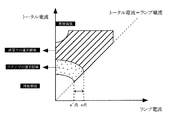
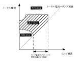
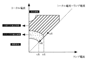
しかしながら、このランプ電流と予熱電流とを加えたトータル電流(フィラメントに流れる電流即ちリード線電流)が多過ぎた場合、図9に示すように、蒸発領域と呼ばれるエミッターが蒸発してしまう領域に入ってしまい、エミッターの消耗が通常よりも激しくなってしまう。また逆にトータル電流が少な過ぎると飛散(スパッタ)領域と呼ばれる、エミッターが固まった状態で飛散していく領域に入ってしまい、結果として早期黒化を招き、短寿命の原因となっていた。
【0004】
このため、従来の安定器の設計においては、最適なランプフィラメントのスポット温度になるように、ランプ電流と予熱電流の流れる量が図9の斜線で示した適正領域になるように設計する必要があった。
【0005】
ところが、定常点灯時における常時予熱電流はフィラメント温度の最適化には寄与するものの、反面フィラメントロスを招いてしまい、高効率化の妨げとなってしまう。そこで最近ではランプ電流のみでフィラメントのスポット温度を満足できるように設計することにより予熱電流をカットして高効率化を図っている。
【0006】
すなわち、図9において、ランプ電流だけでトータル電流を満足する領域では、予熱電流を流さなくても適正領域であり、効率を高めるにはトータル電流=ランプ電流で動作させる方が良い。この領域よりもランプ電流が少ない領域では、ランプ電流が減少するにつれて予熱電流を増加させて、トータル電流を増やす必要がある。なお、ランプ電流が特に少ない領域では予熱電流とランプ電流を加えたトータル電流の適正領域の上限が減少して行き、適正領域が狭くなっている。
【0007】
【発明が解決しようとする課題】
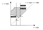
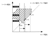
定常時におけるランプ電流が異特性となるランプ(例えば直管ランプとツインランプ)を、上述のような定常点灯時の予熱電流をカットする方式の放電灯点灯装置を用いて点灯させた場合、ランプの種類によって点灯時のランプ電流が異なる(同一仕様の安定器で直管ランプとツインランプを点灯させた場合、直管ランプの方がツインランプよりもランプ電流が大きくなる)ため、図10のa点に示すようにランプ電流だけで適正領域を満たす場合(直管ランプ接続時)と、b点に示すようにランプ電流だけではランプのトータル電流が足りずにスパッタ領域に入ってしまう場合(ツインランプ接続時)とにまたがる可能性がある。そのため、定常点灯時の予熱電流をカットする方式を用いた放電灯点灯装置において、このような異特性を持つランプを適合負荷とする場合には、以下に示す2つの手段のうちどちらか一つを満足しなければならない。
【0008】
まず、一つ目は図11の矢印で示すように、ツインランプの定常時における電流値がスパッタ領域に入らないように(b点からb’点へと)出力を上げることである。しかしながら、このような設計をした場合、定常時の直管ランプの電流値が(a点からa’点へと)さらに大きくなってしまうため、直管ランプを接続した時に必要以上の光が出てしまう、あるいは電流の増加に伴い使用している電子部品の温度が上昇してしまうという問題が生じてしまう。特に電子部品の温度上昇は放電灯点灯装置の寿命にも関係してくるため、好ましくない。また、a’点では逆に蒸発領域に近づく方向なので、出力を上げすぎた場合には蒸発領域に入ってしまう恐れも出てきてしまう。
【0009】
二つ目にはランプのフィラメント構造を変更し、図12に示すようにツインランプの予熱電流の適正領域を広げることである。しかしながらフィラメント構造が異なる結果、先行予熱時における必要予熱電流が変わり、点灯時の予熱電流の設計だけでなく先行予熱時の予熱電流の設計までも困難になる。さらに、上記予熱カット方式の安定器においては予熱カットを行うランプ電流値をd点(直管ランプにおける適正領域とスパッタ領域の境界点)に合わせる設計としなくてはならず、もし負荷としてツインランプを接続した場合にはc点(ツインランプにおける適正領域とスパッタ領域の境界点)〜d点の間においてはもともとランプ電流だけで適正領域を満足できるにも関わらず予熱電流を供給するため、結果として余分なフィラメントロスを生じてしまう。
【0010】
一方、調光機能を併せ持った放電灯点灯装置では、調光時に著しくランプ電流が減少してしまうため、ランプ電流のみでトータル電流を満足させるという予熱カット方式ではどうしてもスパッタ領域に入ってしまうことになる。
【0011】
本発明は上述のような点に鑑みてなされたものであり、特性の異なる複数の熱陰極型放電ランプを適合負荷とする放電灯点灯装置において、予熱電流とランプ電流を加えたトータル電流が適正領域となる範囲で余分な予熱電流をカットして効率を高めることを課題とする。
【0012】
【課題を解決するための手段】
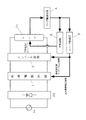
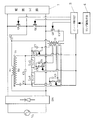
図1は本発明の放電灯点灯装置の基本構成図である。図中、Vsは商用交流電源、DBは全波整流器、Laは蛍光灯などの熱陰極型放電ランプ、1は直流電源回路、2はインバータ回路、3はインバータ制御部、4はランプ識別手段、5は予熱回路である。インバータ制御部3はランプ識別手段4による識別結果を受けて、インバータ回路2の発振周波数あるいはスイッチングのデューティの制御もしくは直流電源回路1の直流電源電圧制御を行う。また、予熱回路5はランプ識別手段4による識別結果を受けて、ランプ負荷Laの予熱電流のオン/オフを行う。
【0013】
本発明によれば、図2のa点に示すように、ランプ電流のみでフィラメントのスポット温度が適正領域を満足する場合は、予熱電流をカットしてフィラメントロスを低減し、効率化を図る。また、図2のb点に示すように、ランプ電流だけでは適正領域を満足できない(飛散領域に入る)場合には、図2のb”点に示すように、予熱電流を加える、もしくは図2のb’点に示すように、ランプ電流を増加させて、インバータのトータル電流(予熱電流+ランプ電流)が適正領域に来るような制御を行うものである。
【0014】
そのために、図1に示すように、放電灯点灯装置にランプ識別手段4を設けておき、識別したランプの種類に応じてこれまで定常点灯時にカットしていた常時予熱電流を連続的または間欠的に供給する、またはインバータ回路1の発振周波数、スイッチングのデューティ、あるいは直流電源回路2の直流電圧を制御することにより、ランプ電流が適正領域まで来るように出力を変化させる。
【0015】
もしくは、ランプ識別手段の代わりにランプ電流を常にモニターする手段を設けておき、図3に示すように、このモニターしている電流値が適正領域とスパッタ領域の境界となるランプ電流値(e点)よりも小さくなった場合には、予熱電流の供給あるいはインバータの出力制御(ランプ電流の増加)を行う。また、モニターしている電流値が図3のe点以上であれば、ランプ電流だけで適正領域を満足できるので、予熱電流をカットしてフィラメントロスを低減し、効率を改善するものである。
【0016】
さらに、異なったフィラメント構造を有するランプを適合負荷とした場合には、装着するランプの種類によって予熱カットすべき範囲(ランプ電流のみで適正領域を満足できる範囲)が異なるため、ランプ識別手段とランプ電流モニター手段を併せ持ち、ランプを識別した後、図4に示すように、ランプの種類に応じて前記制御を行うランプ電流のレベルを変化させる。図4の例では、直管ランプについてはe点で、また、ツインランプについてはe‘点で動作が切り替わるように制御する。直管ランプが接続されている場合の動作は図3と同様である。また、ツインランプが接続されている場合には、モニターしているランプ電流値がe’点よりも小さくなった場合に予熱電流の供給あるいはインバータの出力制御(ランプ電流の増加)を行うことによりトータル電流が適正領域に来るように制御し、ランプ電流値がe’点以上であれば、予熱電流をカットしてフィラメントロスを低減し、効率を改善する。
【0017】
これらの手段を用いることにより、装着ランプの種類、特性、周囲の環境、調光レベルなどに関わらず、常に適正領域でフィラメントのヒーティングができ、スパッタによる早期黒化を防止することができる。また、ランプ電流だけでトータル電流が適正領域を満たす場合には予熱電流をカットする制御を行っているため、定常点灯時のフィラメントロスの低減に伴う高効率化も達成することができる。
【0018】
【発明の実施の形態】
(実施の形態1)
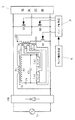
本発明の第1の実施の形態を図5に示す。図5に示す回路では、交流電源Vsに全波整流器DBが接続され、この全波整流器DBにはインバータ回路及び電源回路1が接続されている。インバータ回路は直列接続された二つのスイッチング素子Q1,Q2を備え、一方のスイッチング素子Q2の両端にはリーケージトランスT1の1次巻線n1、直流カット用コンデンサC2の直列回路が接続されている。さらに、リーケージトランスT1の2次巻線n2には直流カット用コンデンサC4と共振コンデンサC3の直列回路が接続され、共振コンデンサC3と並列にランプLa1,La2の直列回路が接続されている。共振コンデンサC3はリーケージトランスT1のリーケージインダクタンスと共に共振回路を構成する。スイッチング素子Q1,Q2はインバータ制御部3によって交互にオン、オフを繰り返す。スイッチング電流のオン、オフ動作によりスイッチング素子Q1,Q2の接続点に発生する矩形波電圧により前記共振回路に共振電圧が流れる。
【0019】
次に、予熱回路の構成について説明する。リーケージトランスT1と直流カット用コンデンサC2との接続点とスイッチング素子Q2と全波整流器DBとの接続点の間には、予熱トランスT2の1次巻線とコンデンサC1、及びスイッチング素子Q3の直列回路が接続されている。インバータ制御部3によってスイッチング素子Q3がオンしている間は予熱トランスT2とコンデンサC1の共振によって電流が流れる。また、予熱トランスT2の2次側は直流カット用コンデンサC5,C6,C7を介して各ランプLa1,La2のフィラメントが接続されており、これによってフィラメントの予熱を行う構成となっている。なお、スイッチング素子Q3は点灯時にはインバータ制御部3によってオフとなるように制御されており、フィラメントにおけるロスを低減するようにしている。
【0020】
次に、この実施の形態の動作について説明する。この実施の形態では前記放電灯点灯装置にランプの種類を識別するランプ識別手段4が接続されており、電源が投入されると何らかの手段により接続されているランプLa1,La2の種類を識別する。ここで、この放電灯点灯装置は定常点灯時のランプ電流の値が異特性となるランプを適合負荷としており、もし接続したランプのランプ電流がスパッタ領域に入るような場合、ランプ識別手段4からインバータ制御部3に制御信号を出して、スイッチング素子Q3をオンさせ、予熱電流を供給するような制御を行う。あるいは、インバータ回路のスイッチング素子Q1,Q2の発振周波数や、スイッチングのデューティを変化させることによって出力を増大させて、ランプ電流が増えるような制御を行う。これにより、フィラメントに流れる電流がスパッタ領域に入ることを防止している。なお、フィラメントに流れる電流が蒸発領域に入る場合も同様に、今度は出力を下げる制御を行うことにより、適正領域に入るように制御している。
【0021】
(実施の形態2)
本発明の第2の実施の形態を図6に示す。放電灯点灯装置の基本的な回路構成、動作については実施の形態1と同一のため説明を省略する。図6に示す回路では、図5の構成に加え、さらに予熱回路に直列にインピーダンスZが接続されており、インピーダンスZにはスイッチング素子Q4が並列に接続されており、インバータ制御部3からの制御信号によって、予熱回路に接続されたり、短絡されたりして、予熱回路のインピーダンスを可変とする。
【0022】
次に、この実施の形態の動作について説明する。この実施の形態ではランプの種類を識別するランプ識別手段4が接続されており、電源が投入されると何らかの手段により接続されているランプLa1,La2の種類を識別する。ここで、この放電灯点灯装置は定常点灯時のランプ電流の値が異特性となるランプを適合負荷としており、もし接続したランプのランプ電流がスパッタ領域に入るような場合、ランプ識別手段4からインバータ制御部3に制御信号を出して、スイッチング素子Q3をオンさせ、予熱電流を供給するような制御を行う。あるいは、インバータ回路1のスイッチング素子Q1,Q2の発振周波数や、スイッチングのデューティを変化させることによって出力を増大させて、ランプ電流が増えるような制御を行う。これにより、フィラメントに流れる電流がスパッタ領域に入ることを防止している。なお、フィラメントに流れる電流が蒸発領域に入る場合も同様に、今度は出力を下げる制御を行うことにより、適正領域に入るようにしている。
【0023】
さらに、この実施の形態においては予熱回路にインピーダンスZを挿入することで予熱回路のインピーダンスを可変とし、予熱電流の大きさを調節することができる。ここで、インピーダンスZの大きさを各負荷に応じた予熱電流が流れる大きさに設定することで、所望の予熱電流を得ることができるため、特にランプごとに先行予熱電流が異なる場合にそれぞれの負荷に応じた最適な先行予熱電流を流すことができるという効果を得ることができる。
【0024】
(実施の形態3)
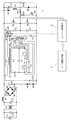
本発明の第3の実施の形態を図7に示す。ダイオードD1〜D4のブリッジ回路は全波整流器を構成しており、その交流入力端子はフィルター回路を介して商用電源Vsに接続されている。フィルター回路はフィルターチョークL1とフィルターコンデンサC12,C13およびフィルタートランスT3で構成されており、インバータ回路の高周波ノイズが商用電源Vsに漏洩することを防止している。ダイオードD1〜D4よりなる全波整流器の直流出力端子には、小容量のコンデンサC8が並列接続されると共に、ダイオードD5,D6の直列回路を介してスイッチング素子Q1,Q2の直列回路が接続されている。ダイオードD5には入力電流歪改善用コンデンサC14が並列接続されている。ダイオードD5,D6の接続点とスイッチング素子Q1,Q2の接続点の間には、リーケージトランスT1の1次巻線n1と直流カット用コンデンサC2の直列回路が接続されている。スイッチング素子Q2には小容量のコンデンサC0が並列接続されている。リーケージトランスT1の2次巻線n2には直流カット用のコンデンサC4を介して共振コンデンサC3が接続されており、共振コンデンサC3の両端にはランプLa1,La2の直列回路が接続されている。共振コンデンサC3はリーケージトランスT1のリーケージインダクタンスと共に共振回路を構成する。一方のランプLa1の両フィラメントの非電源側端子間には逐次点灯用のコンデンサC9が並列接続されている。各ランプLa1,La2のフィラメントにはコンデンサC5,C6,C7を介して予熱トランスT2の予熱巻線(各2次巻線)が接続されている。予熱トランスT2の1次巻線の一端はスイッチ手段SWの端子Aに接続されており、他端はコンデンサC1を介してスイッチング素子Q2とダイオードD5の接続点に接続されている。スイッチ手段SWはインバータ制御部3からの制御信号により端子Aを端子Bまたは端子Cのいずれかに接続するか、もしくはオープンとするように切替制御される。スイッチ手段SWの端子BはリーケージトランスT1の1次巻線n1と直流カット用コンデンサC2の接続点に接続されており、端子CはダイオードD5,D6の接続点に接続されている。
【0025】
スイッチング素子Q1,Q2の直列回路の両端には小容量のコンデンサC10と電源回路1が接続されている。この電源回路1は、インバータ回路のスイッチング素子Q2をチョッパー用のスイッチング素子として兼用して平滑コンデンサC11に直流電圧を充電し、整流出力電圧が低い期間にインバータ回路に供給するものである。ダイオードD1〜D4よりなる全波整流器の直流出力電圧が高い期間において、スイッチング素子Q2がオンのとき、全波整流器から平滑コンデンサC11、インダクタL2、ダイオードD9、スイッチング素子Q2の経路で電流が流れて平滑コンデンサC11が充電され、また、スイッチング素子Q2がオフすると、インダクタL2の蓄積エネルギーによる回生電流がインダクタL2からダイオードD7を介して平滑コンデンサC11に流れて平滑コンデンサC11が充電される。ダイオードD1〜D4よりなる全波整流器の直流出力電圧が低い期間においては、平滑コンデンサC11の直流電圧がインダクタL2とダイオードD8を介してスイッチング素子Q1,Q2の直列回路に供給される。なお、電源投入直後の平滑コンデンサC11の充電電圧が低い期間では、スイッチング素子Q1,Q2の動作開始前に、スイッチング素子Q8がオンとなり、抵抗R1を介して突入電流を抑制しながら平滑コンデンサC11を充電し、スイッチング素子Q1,Q2の動作開始後はスイッチング素子Q8はオフとなる。
【0026】
この実施の形態の動作については実施の形態2と同一のため重複する説明は省略するが、予熱電流の切り替えの仕組みが実施の形態2とは異なる。この実施の形態においては、スイッチ手段SWの端子Aをオープン状態で予熱電流をカットするか、もしくは端子BまたはCのいずれかと接続してそれぞれ所定の予熱電流を供給するかはランプ識別手段4からの信号を受けてインバータ制御部3で切替制御される。ここで、端子Bと端子Cとでは電圧振幅が異なっており、振幅の高い端子Bの方に接続された時の方が予熱電流の供給量は多くなる。このように電圧振幅の異なる2つの電圧供給源を切り替えることにより予熱回路の供給電圧を可変とする。
【0027】
この実施の形態では、予熱回路の供給電圧の切替回路を具備することにより、予熱カット手段と予熱電流の大きさを調整する回路とが一体化できた上、コンデンサC14の定数、予熱回路への印加電圧、予熱回路の定数を最適に設定することにより所望の予熱電流を得ることができるため、特に先行予熱電流が異なる場合にそれぞれの負荷に応じた最適な先行予熱電流を流すことができるという効果を得ることができる。
【0028】
(実施の形態4)
本発明の第4の実施の形態を図8に示す。放電灯点灯装置の基本的な回路構成、動作については実施の形態1と同一構成のため説明を省略する。図8に示す回路では一般的な放電灯点灯装置に加え、予熱トランスT2の2次側に接続されている直流カット用コンデンサC5,C6,C7と並列にスイッチ素子Q5,Q6,Q7とコンデンサC15,C16,C17の直列回路が接続され、スイッチ素子Q5,Q6,Q7のオン、オフによって予熱回路の直流カット用コンデンサの容量を変化させることができる。
【0029】
この実施の形態においても上述の実施の形態1と同様の制御を行うが、特に本例では予熱回路の直流カット用コンデンサの容量を可変とすることにより、実施の形態2と同様、予熱電流の大きさを変化させることができるため、コンデンサの容量調節によって所望の予熱電流を得ることができる。よって、特に先行予熱電流が異なる場合にそれぞれの負荷に応じた最適な先行予熱電流を流すことができるという効果も有する。
【0030】
【発明の効果】
本発明においては、これまでランプの種類に関係なく予熱電流をカットしていたため、接続するランプの種類によってはスパッタによる短寿命になっていたところを、各ランプに応じた予熱制御を行うことにより、1種類の放電灯点灯装置で特性の違う異種のランプを常に最適なフィラメント温度で点灯させることが可能となる。これにより蒸発やスパッタによる短寿命を防ぐことができる。また、ランプ電流のみで適正領域を満足できる場合には予熱電流をカットする制御としたため、常に予熱電流を流し続ける場合よりもフィラメントロスを低減することができる。
【図面の簡単な説明】
【図1】本発明の基本構成を示すブロック回路図である。
【図2】本発明の第1の動作説明図である。
【図3】本発明の第2の動作説明図である。
【図4】本発明の第3の動作説明図である。
【図5】本発明の実施の形態1の回路図である。
【図6】本発明の実施の形態2の回路図である。
【図7】本発明の実施の形態3の回路図である。
【図8】本発明の実施の形態4の回路図である。
【図9】熱陰極型放電灯のフィラメント予熱の適正な領域を示す説明図である。
【図10】第1の従来例の動作説明図である。
【図11】第2の従来例の動作説明図である。
【図12】第3の従来例の動作説明図である。
【符号の説明】
Vs 交流電源
DB 全波整流器
1 直流電源回路
2 インバータ回路
3 インバータ制御部
4 ランプ識別手段
5 予熱回路
La ランプ(熱陰極型放電灯)[0001]
BACKGROUND OF THE INVENTION
The present invention relates to a discharge lamp lighting device having a plurality of hot-cathode discharge lamps having different characteristics as compatible loads.
[0002]
[Prior art]
In general, the life of a hot cathode type discharge lamp refers to the time when the emitter applied to the filament is consumed. This emitter will naturally decrease as it is lit using the discharge lamp lighting device, but the rate of decrease depends on the spot temperature of the lamp filament at the time of lighting. If the temperature is too high or too low, the rate of decrease will increase. When starting and lighting a lamp with a conventional general discharge lamp lighting device, a preheating current is added to the lamp current to heat the lamp filament spot temperature to an appropriate temperature. When the lamp current is extremely small, such as when the light is dimmed or when the light is adjusted, an optimum filament temperature is obtained by supplying a current called a pre-heating current to the filament.
[0003]
However, if the total current (the current flowing through the filament, that is, the lead wire current) obtained by adding the lamp current and the preheating current is too large, as shown in FIG. 9, the emitter enters an area where the emitter evaporates. As a result, the exhaustion of the emitter becomes more intense than usual. On the other hand, if the total current is too small, it enters a region where the emitter is scattered in a solid state, called a scattering (sputtering) region, resulting in premature blackening and a short life.
[0004]
For this reason, in the conventional ballast design, it is necessary to design the lamp current and the preheating current to flow in an appropriate region shown by the oblique lines in FIG. 9 so that the spot temperature of the lamp filament is optimum. there were.
[0005]
However, the constant preheating current during steady lighting contributes to optimization of the filament temperature, but on the other hand, filament loss is caused, which hinders high efficiency. Therefore, recently, by designing the lamp so that the filament spot temperature can be satisfied only by the lamp current, the preheating current is cut to increase the efficiency.
[0006]
That is, in FIG. 9, the region where the total current is satisfied only with the lamp current is an appropriate region without supplying the preheating current, and it is better to operate with the total current = lamp current in order to increase the efficiency. In a region where the lamp current is smaller than this region, it is necessary to increase the total current by increasing the preheating current as the lamp current decreases. In the region where the lamp current is particularly small, the upper limit of the appropriate region of the total current including the preheating current and the lamp current is decreasing, and the appropriate region is narrowed.
[0007]
[Problems to be solved by the invention]
When a lamp (for example, a straight tube lamp and a twin lamp) with different lamp currents at regular times is lit using a discharge lamp lighting device that cuts the preheating current during steady lighting as described above, the lamp The lamp current at the time of lighting differs depending on the type of lamp (when a straight tube lamp and a twin lamp are lit with a ballast of the same specification, the lamp current of the straight tube lamp is larger than that of the twin lamp). When the appropriate area is satisfied only by the lamp current as shown at point a (when a straight tube lamp is connected), and when the lamp current alone is insufficient as shown by point b, the total current of the lamp enters the sputter region ( (When twin lamps are connected). Therefore, in a discharge lamp lighting device using a method of cutting the preheating current during steady lighting, when a lamp having such a different characteristic is used as an applicable load, one of the following two means is used. Must be satisfied.
[0008]
First, as shown by the arrows in FIG. 11, the output is increased so that the current value in the steady state of the twin lamp does not enter the sputtering region (from point b to point b '). However, when such a design is used, the current value of the straight tube lamp in a steady state becomes larger (from point a to point a ′), so that more light than necessary is emitted when the straight tube lamp is connected. In other words, the temperature of the electronic component used increases as the current increases. In particular, an increase in the temperature of the electronic component is also not preferable because it is related to the life of the discharge lamp lighting device. Further, since the a ′ point is in the direction of approaching the evaporation region, if the output is increased too much, there is a risk of entering the evaporation region.
[0009]
The second is to change the filament structure of the lamp and widen the appropriate region of the preheating current of the twin lamp as shown in FIG. However, as a result of the different filament structure, the required preheating current at the time of preceding preheating changes, and it becomes difficult not only to design the preheating current at the time of lighting but also to design the preheating current at the time of preceding preheating. Furthermore, in the preheat-cut type ballast described above, the lamp current value for preheat cut must be designed to match the point d (the boundary point between the appropriate region and the sputter region in a straight tube lamp), and if the load is a twin lamp Is connected between point c (boundary point of appropriate region and sputter region in twin lamps) and point d, although the appropriate region can be satisfied by the lamp current alone, the preheating current is supplied. As a result, extra filament loss will occur.
[0010]
On the other hand, in a discharge lamp lighting device that also has a dimming function, the lamp current decreases significantly during dimming, so the preheating cut method that satisfies the total current with only the lamp current inevitably enters the sputter region. Become.
[0011]
The present invention has been made in view of the above points, and in a discharge lamp lighting device having a plurality of hot cathode type discharge lamps having different characteristics as suitable loads, the total current obtained by adding the preheating current and the lamp current is appropriate. It is an object to increase the efficiency by cutting an extra preheating current in an area.
[0012]
[Means for Solving the Problems]
FIG. 1 is a basic configuration diagram of a discharge lamp lighting device according to the present invention. In the figure, Vs is a commercial AC power supply, DB is a full-wave rectifier, La is a hot cathode discharge lamp such as a fluorescent lamp, 1 is a DC power supply circuit, 2 is an inverter circuit, 3 is an inverter control unit, 4 is a lamp identification means,
[0013]
According to the present invention, as shown at point a in FIG. 2, when the spot temperature of the filament satisfies the appropriate region only with the lamp current, the preheating current is cut to reduce the filament loss and increase the efficiency. Further, as shown at point b in FIG. 2, when the appropriate region cannot be satisfied only by the lamp current (enters the scattering region), a preheating current is applied as shown at point b ″ in FIG. As shown at point b ', the lamp current is increased, and control is performed so that the total current of the inverter (preheating current + lamp current) is in an appropriate region.
[0014]
For this purpose, as shown in FIG. 1, the discharge lamp lighting device is provided with lamp identification means 4, and the continuous preheating current that has been cut at the time of steady lighting according to the type of the identified lamp is continuously or intermittently applied. , Or by controlling the oscillation frequency of the
[0015]
Alternatively, a means for constantly monitoring the lamp current is provided instead of the lamp identification means, and as shown in FIG. 3, the lamp current value (point e) at which the monitored current value becomes the boundary between the appropriate area and the sputtering area is provided. ), The preheating current is supplied or the inverter output is controlled (increasing the lamp current). If the current value monitored is equal to or greater than the point e in FIG. 3, the lamp current alone can satisfy the appropriate region, so the preheating current is cut to reduce filament loss and improve efficiency.
[0016]
Furthermore, when a lamp having a different filament structure is used as a suitable load, the range to be preheated cut (the range that can satisfy the appropriate area only by the lamp current) differs depending on the type of the mounted lamp. As shown in FIG. 4, the lamp current level to be controlled is changed according to the type of the lamp after the lamp is identified and the lamp is identified. In the example of FIG. 4, control is performed so that the operation is switched at point e for a straight tube lamp and at point e ′ for a twin lamp. The operation when a straight tube lamp is connected is the same as in FIG. In addition, when a twin lamp is connected, when the monitored lamp current value becomes smaller than the point e ′, by supplying a preheating current or controlling the output of the inverter (increasing the lamp current) Control is made so that the total current is in an appropriate region, and if the lamp current value is equal to or greater than the point e ′, the preheating current is cut to reduce filament loss and improve efficiency.
[0017]
By using these means, the filament can always be heated in an appropriate region regardless of the type, characteristics, ambient environment, dimming level, etc. of the mounted lamp, and premature blackening due to sputtering can be prevented. In addition, when the total current satisfies the appropriate region with only the lamp current, control is performed to cut the preheating current, so that high efficiency can be achieved along with reduction of filament loss during steady lighting.
[0018]
DETAILED DESCRIPTION OF THE INVENTION
(Embodiment 1)
A first embodiment of the present invention is shown in FIG. In the circuit shown in FIG. 5, a full-wave rectifier DB is connected to an AC power supply Vs, and an inverter circuit and a
[0019]
Next, the configuration of the preheating circuit will be described. Between the connection point of the leakage transformer T1 and the DC cut capacitor C2 and the connection point of the switching element Q2 and the full-wave rectifier DB, a series circuit of the primary winding of the preheating transformer T2, the capacitor C1, and the switching element Q3. Is connected. While the switching element Q3 is turned on by the
[0020]
Next, the operation of this embodiment will be described. In this embodiment, a
[0021]
(Embodiment 2)
A second embodiment of the present invention is shown in FIG. Since the basic circuit configuration and operation of the discharge lamp lighting device are the same as those of the first embodiment, description thereof is omitted. In the circuit shown in FIG. 6, in addition to the configuration of FIG. 5, an impedance Z is connected in series to the preheating circuit, and a switching element Q4 is connected in parallel to the impedance Z. Depending on the signal, the impedance of the preheating circuit is made variable by being connected to the preheating circuit or being short-circuited.
[0022]
Next, the operation of this embodiment will be described. In this embodiment, lamp identification means 4 for identifying the type of lamp is connected, and when the power is turned on, the type of lamps La1 and La2 connected is identified by some means. Here, the discharge lamp lighting device uses a lamp having a different lamp current value during steady lighting as a suitable load. If the lamp current of the connected lamp enters the sputter region, the lamp identification means 4 A control signal is output to the
[0023]
Furthermore, in this embodiment, the impedance of the preheating circuit can be made variable by inserting the impedance Z into the preheating circuit, and the magnitude of the preheating current can be adjusted. Here, since the desired preheating current can be obtained by setting the magnitude of the impedance Z to such a magnitude that the preheating current according to each load flows, It is possible to obtain an effect that an optimum preceding preheating current corresponding to the load can flow.
[0024]
(Embodiment 3)
A third embodiment of the present invention is shown in FIG. The bridge circuit of the diodes D1 to D4 constitutes a full-wave rectifier, and its AC input terminal is connected to the commercial power supply Vs via a filter circuit. The filter circuit includes a filter choke L1, filter capacitors C12 and C13, and a filter transformer T3, and prevents high-frequency noise of the inverter circuit from leaking to the commercial power supply Vs. A small-capacitance capacitor C8 is connected in parallel to the DC output terminal of the full-wave rectifier composed of diodes D1 to D4, and a series circuit of switching elements Q1 and Q2 is connected via a series circuit of diodes D5 and D6. Yes. An input current distortion improving capacitor C14 is connected in parallel to the diode D5. A series circuit of the primary winding n1 of the leakage transformer T1 and the DC cut capacitor C2 is connected between the connection point of the diodes D5 and D6 and the connection point of the switching elements Q1 and Q2. A small-capacitance capacitor C0 is connected in parallel to the switching element Q2. A resonance capacitor C3 is connected to the secondary winding n2 of the leakage transformer T1 via a DC cut capacitor C4. A series circuit of lamps La1 and La2 is connected to both ends of the resonance capacitor C3. The resonance capacitor C3 forms a resonance circuit together with the leakage inductance of the leakage transformer T1. A capacitor C9 for sequential lighting is connected in parallel between the non-power supply terminals of both filaments of one lamp La1. The preheating windings (respective secondary windings) of the preheating transformer T2 are connected to the filaments of the lamps La1 and La2 through capacitors C5, C6, and C7. One end of the primary winding of the preheating transformer T2 is connected to the terminal A of the switch means SW, and the other end is connected to a connection point between the switching element Q2 and the diode D5 via the capacitor C1. The switch means SW is controlled to be switched so that the terminal A is connected to either the terminal B or the terminal C or is opened by a control signal from the
[0025]
A small-capacitance capacitor C10 and a
[0026]
Since the operation of this embodiment is the same as that of the second embodiment, a redundant description is omitted, but the mechanism for switching the preheating current is different from that of the second embodiment. In this embodiment, whether the preheating current is cut while the terminal A of the switch means SW is open or connected to either the terminal B or C to supply a predetermined preheating current from the lamp identification means 4. Is switched by the
[0027]
In this embodiment, by providing a switching circuit for the supply voltage of the preheating circuit, the preheating cutting means and the circuit for adjusting the magnitude of the preheating current can be integrated, and the constant of the capacitor C14 and the preheating circuit can be connected to the preheating circuit. Since the desired preheating current can be obtained by optimally setting the applied voltage and the constant of the preheating circuit, it is possible to flow the optimum preceding preheating current according to each load particularly when the preceding preheating current is different. An effect can be obtained.
[0028]
(Embodiment 4)
A fourth embodiment of the present invention is shown in FIG. Since the basic circuit configuration and operation of the discharge lamp lighting device are the same as those in the first embodiment, description thereof is omitted. In the circuit shown in FIG. 8, in addition to a general discharge lamp lighting device, switching elements Q5, Q6, Q7 and a capacitor C15 are connected in parallel with DC cutting capacitors C5, C6 and C7 connected to the secondary side of the preheating transformer T2. , C16 and C17 are connected, and the capacitance of the DC cut capacitor of the preheating circuit can be changed by turning on and off the switch elements Q5, Q6 and Q7.
[0029]
In this embodiment, the same control as in the first embodiment is performed, but in this example, the capacity of the DC cutting capacitor of the preheating circuit is made variable so that the preheating current can be controlled as in the second embodiment. Since the size can be changed, a desired preheating current can be obtained by adjusting the capacitance of the capacitor. Therefore, particularly when the preceding preheating current is different, there is also an effect that an optimum preceding preheating current corresponding to each load can be supplied.
[0030]
【The invention's effect】
In the present invention, since the preheating current has been cut regardless of the type of the lamp so far, depending on the type of the lamp to be connected, the short life due to the sputtering is performed by performing the preheating control according to each lamp. Different types of lamps having different characteristics in one type of discharge lamp lighting device can always be lit at the optimum filament temperature. This can prevent a short life due to evaporation or sputtering. In addition, when the appropriate region can be satisfied only by the lamp current, the preheating current is controlled to be cut, so that the filament loss can be reduced as compared with the case where the preheating current is constantly kept flowing.
[Brief description of the drawings]
FIG. 1 is a block circuit diagram showing a basic configuration of the present invention.
FIG. 2 is a diagram illustrating a first operation of the present invention.
FIG. 3 is a diagram illustrating a second operation of the present invention.
FIG. 4 is a diagram illustrating a third operation of the present invention.
FIG. 5 is a circuit diagram according to the first embodiment of the present invention.
FIG. 6 is a circuit diagram of
FIG. 7 is a circuit diagram of
FIG. 8 is a circuit diagram according to a fourth embodiment of the present invention.
FIG. 9 is an explanatory view showing an appropriate region for filament preheating of a hot cathode discharge lamp.
FIG. 10 is an operation explanatory diagram of a first conventional example.
FIG. 11 is an operation explanatory diagram of a second conventional example.
FIG. 12 is an operation explanatory diagram of a third conventional example.
[Explanation of symbols]
Vs AC power supply DB
Claims (10)
Priority Applications (1)
| Application Number | Priority Date | Filing Date | Title |
|---|---|---|---|
| JP2001366634A JP3801034B2 (en) | 2001-11-30 | 2001-11-30 | Discharge lamp lighting device |
Applications Claiming Priority (1)
| Application Number | Priority Date | Filing Date | Title |
|---|---|---|---|
| JP2001366634A JP3801034B2 (en) | 2001-11-30 | 2001-11-30 | Discharge lamp lighting device |
Publications (2)
| Publication Number | Publication Date |
|---|---|
| JP2003168582A JP2003168582A (en) | 2003-06-13 |
| JP3801034B2 true JP3801034B2 (en) | 2006-07-26 |
Family
ID=19176503
Family Applications (1)
| Application Number | Title | Priority Date | Filing Date |
|---|---|---|---|
| JP2001366634A Expired - Fee Related JP3801034B2 (en) | 2001-11-30 | 2001-11-30 | Discharge lamp lighting device |
Country Status (1)
| Country | Link |
|---|---|
| JP (1) | JP3801034B2 (en) |
Families Citing this family (5)
| Publication number | Priority date | Publication date | Assignee | Title |
|---|---|---|---|---|
| JP2005310755A (en) * | 2004-03-23 | 2005-11-04 | Toshiba Lighting & Technology Corp | Discharge lamp lighting device and lighting device |
| DE202005013753U1 (en) * | 2005-08-31 | 2005-11-17 | Patent-Treuhand-Gesellschaft für elektrische Glühlampen mbH | Electronic ballast for operating discharge lamp, has control device to ignite lamp discharging in non-repetitive process for parameter e.g. voltage, that is correlated to temperature of electrodes during measurement of parameter |
| DE202005013754U1 (en) * | 2005-08-31 | 2005-11-17 | Patent-Treuhand-Gesellschaft für elektrische Glühlampen mbH | Electronic control gear for operating discharge lamp, has measuring device to measure parameter that correlates to increased electrode temperature, and control device to react to temperature by adjustment of operating parameter of gear |
| WO2007086455A1 (en) * | 2006-01-25 | 2007-08-02 | Toshiba Lighting & Technology Corporation | Discharge lamp operating device and illuminator |
| JP2012028039A (en) * | 2010-07-20 | 2012-02-09 | Panasonic Electric Works Co Ltd | Discharge lamp lighting device and luminaire with discharge lamp lighting device |
-
2001
- 2001-11-30 JP JP2001366634A patent/JP3801034B2/en not_active Expired - Fee Related
Also Published As
| Publication number | Publication date |
|---|---|
| JP2003168582A (en) | 2003-06-13 |
Similar Documents
| Publication | Publication Date | Title |
|---|---|---|
| US8294384B2 (en) | Dimming electronic ballast with preheat current control | |
| WO1998047323A1 (en) | Discharge lamp lighting device and illumination device | |
| JP3532760B2 (en) | Discharge lamp lighting device | |
| JP3832074B2 (en) | Discharge lamp lighting device | |
| JP3801034B2 (en) | Discharge lamp lighting device | |
| JP4241358B2 (en) | Discharge lamp lighting device, lighting fixture and lighting system | |
| KR100283312B1 (en) | Fluorescent Flasher | |
| JP4547847B2 (en) | Discharge lamp lighting device | |
| JP4058569B2 (en) | Discharge lamp lighting device and lighting device | |
| JP2001345195A (en) | Discharge lamp lighting device | |
| JP2658042B2 (en) | Discharge lamp lighting device | |
| JP2002231483A (en) | Discharge lamp lighting device | |
| JP2000164386A (en) | Discharge lamp lighting device | |
| JP2005259454A (en) | Discharge lamp lighting device | |
| JP4140219B2 (en) | Discharge lamp lighting device | |
| JP3834892B2 (en) | Discharge lamp lighting device | |
| JP4207702B2 (en) | Discharge lamp lighting device | |
| JP2005310755A (en) | Discharge lamp lighting device and lighting device | |
| JP2008166297A (en) | Discharge lamp lighting device | |
| JP2008277149A (en) | Discharge lamp lighting device | |
| JP2005310735A (en) | Discharge lamp lighting device and lighting device | |
| JP2005235619A (en) | Discharge lamp lighting device | |
| JP2000036398A (en) | Discharge lamp lighting device | |
| JP2003168583A (en) | Discharge lamp lighting device | |
| JP2011034719A (en) | Discharge lamp lighting device and lighting system |
Legal Events
| Date | Code | Title | Description |
|---|---|---|---|
| A621 | Written request for application examination |
Free format text: JAPANESE INTERMEDIATE CODE: A621 Effective date: 20040826 |
|
| A977 | Report on retrieval |
Free format text: JAPANESE INTERMEDIATE CODE: A971007 Effective date: 20050708 |
|
| A131 | Notification of reasons for refusal |
Free format text: JAPANESE INTERMEDIATE CODE: A131 Effective date: 20050719 |
|
| A521 | Written amendment |
Free format text: JAPANESE INTERMEDIATE CODE: A523 Effective date: 20050916 |
|
| TRDD | Decision of grant or rejection written | ||
| A01 | Written decision to grant a patent or to grant a registration (utility model) |
Free format text: JAPANESE INTERMEDIATE CODE: A01 Effective date: 20060411 |
|
| A61 | First payment of annual fees (during grant procedure) |
Free format text: JAPANESE INTERMEDIATE CODE: A61 Effective date: 20060424 |
|
| R150 | Certificate of patent (=grant) or registration of utility model |
Free format text: JAPANESE INTERMEDIATE CODE: R150 |
|
| FPAY | Renewal fee payment (prs date is renewal date of database) |
Free format text: PAYMENT UNTIL: 20090512 Year of fee payment: 3 |
|
| S533 | Written request for registration of change of name |
Free format text: JAPANESE INTERMEDIATE CODE: R313533 |
|
| FPAY | Renewal fee payment (prs date is renewal date of database) |
Free format text: PAYMENT UNTIL: 20090512 Year of fee payment: 3 |
|
| R350 | Written notification of registration of transfer |
Free format text: JAPANESE INTERMEDIATE CODE: R350 |
|
| FPAY | Renewal fee payment (prs date is renewal date of database) |
Free format text: PAYMENT UNTIL: 20100512 Year of fee payment: 4 |
|
| FPAY | Renewal fee payment (prs date is renewal date of database) |
Free format text: PAYMENT UNTIL: 20100512 Year of fee payment: 4 |
|
| FPAY | Renewal fee payment (prs date is renewal date of database) |
Free format text: PAYMENT UNTIL: 20110512 Year of fee payment: 5 |
|
| FPAY | Renewal fee payment (prs date is renewal date of database) |
Free format text: PAYMENT UNTIL: 20120512 Year of fee payment: 6 |
|
| FPAY | Renewal fee payment (prs date is renewal date of database) |
Free format text: PAYMENT UNTIL: 20120512 Year of fee payment: 6 |
|
| FPAY | Renewal fee payment (prs date is renewal date of database) |
Free format text: PAYMENT UNTIL: 20130512 Year of fee payment: 7 |
|
| FPAY | Renewal fee payment (prs date is renewal date of database) |
Free format text: PAYMENT UNTIL: 20130512 Year of fee payment: 7 |
|
| LAPS | Cancellation because of no payment of annual fees |