JP3800520B2 - Semiconductor integrated circuit device and semiconductor device - Google Patents
Semiconductor integrated circuit device and semiconductor device Download PDFInfo
- Publication number
- JP3800520B2 JP3800520B2 JP2002046740A JP2002046740A JP3800520B2 JP 3800520 B2 JP3800520 B2 JP 3800520B2 JP 2002046740 A JP2002046740 A JP 2002046740A JP 2002046740 A JP2002046740 A JP 2002046740A JP 3800520 B2 JP3800520 B2 JP 3800520B2
- Authority
- JP
- Japan
- Prior art keywords
- mosfet
- pair
- transistor
- drain
- circuit
- Prior art date
- Legal status (The legal status is an assumption and is not a legal conclusion. Google has not performed a legal analysis and makes no representation as to the accuracy of the status listed.)
- Expired - Fee Related
Links
Images


Classifications
-
- H—ELECTRICITY
- H03—ELECTRONIC CIRCUITRY
- H03F—AMPLIFIERS
- H03F3/00—Amplifiers with only discharge tubes or only semiconductor devices as amplifying elements
- H03F3/45—Differential amplifiers
- H03F3/45071—Differential amplifiers with semiconductor devices only
- H03F3/45076—Differential amplifiers with semiconductor devices only characterised by the way of implementation of the active amplifying circuit in the differential amplifier
- H03F3/45179—Differential amplifiers with semiconductor devices only characterised by the way of implementation of the active amplifying circuit in the differential amplifier using MOSFET transistors as the active amplifying circuit
- H03F3/4521—Complementary long tailed pairs having parallel inputs and being supplied in parallel
- H03F3/45219—Folded cascode stages
-
- H—ELECTRICITY
- H03—ELECTRONIC CIRCUITRY
- H03F—AMPLIFIERS
- H03F3/00—Amplifiers with only discharge tubes or only semiconductor devices as amplifying elements
- H03F3/72—Gated amplifiers, i.e. amplifiers which are rendered operative or inoperative by means of a control signal
-
- H—ELECTRICITY
- H03—ELECTRONIC CIRCUITRY
- H03F—AMPLIFIERS
- H03F2203/00—Indexing scheme relating to amplifiers with only discharge tubes or only semiconductor devices as amplifying elements covered by H03F3/00
- H03F2203/45—Indexing scheme relating to differential amplifiers
- H03F2203/45396—Indexing scheme relating to differential amplifiers the AAC comprising one or more switches
-
- H—ELECTRICITY
- H03—ELECTRONIC CIRCUITRY
- H03F—AMPLIFIERS
- H03F2203/00—Indexing scheme relating to amplifiers with only discharge tubes or only semiconductor devices as amplifying elements covered by H03F3/00
- H03F2203/45—Indexing scheme relating to differential amplifiers
- H03F2203/45506—Indexing scheme relating to differential amplifiers the CSC comprising only one switch
Description
【0001】
【発明の属する技術分野】
この発明は、半導体集積回路装置に関し、小振幅の入力信号が供給される半導体集積回路装置の入力回路に利用して有効な技術に関するものである。
【0002】
【従来の技術】
小振幅の入力信号を受け、高速に動作する必要のある入力回路には、一般的には差動入力回路が用いられる。しかしながら、入力電圧Vinが、Vin<2×Vth(差動MOSFET、電流源MOSFETのしきい値電圧)のように低くなると、差動MOSFETの共通ソースに設けられた電流源MOSFETの電流が減り、正常動作が行えないという問題を有する。
【0003】
【発明が解決しようとする課題】
本願発明者においては、入力信号が電源電圧あるいは回路の接地電位にシフトしても動作を行うことができるレール・ツー・レール(rail to railは、米国モトラーラ社の登録商標である)回路に着目した。図13は、この発明に先立って検討されたレール・ツー・レール回路の回路図が示されている。この回路は、バイアスP1,P2、N1,N2及びDCP,DCNを必要とし、素子のプロセスバラツキ、例えばPチャネルMOSFETとNチャネルMOSFETの相互コンダクタンス比のバラツキ、入力電圧Vinのシフトを考慮すると、そのまま小振幅、高速入力回路として使用するのが難しい。
【0004】
図14には、米国特許第4,958,133号公報によって提案されている自己バイアス型のレール・ツー・レール回路の回路図が示されている。また、雑誌「トランジスタ技術」2001年3月号第201頁には、オペアンプにレール・ツー・レール回路を用いた例が示されている。これらの回路は、オペアンプとして用いることができても、その信号伝達速度が遅いために、高速動作が要求されるスタティック型RAM(ランダム・アクセス・メモリ)のアドレス信号、クロック信号、各種制御信号を入力するための入力回路としては不向きである。
【0005】
この発明の目的は、低電圧まで安定的に高速動作が可能な入力回路を備えた半導体集積回路装置を提供することにある。この発明の前記ならびにそのほかの目的と新規な特徴は、本明細書の記述および添付図面から明らかになるであろう。
【0006】
【課題を解決するための手段】
本願において開示される発明のうち代表的なものの概要を簡単に説明すれば、下記の通りである。第1入力端子にそれぞれゲートが接続された第1導電型の第1差動MOSFET対及びその共通ソースに設けられて動作電流を形成する第1導電型の第1電流源MOSFETを第1増幅部とし、上記一対の第1入力端子にそれぞれゲートが接続された第2導電型の第2差動MOSFET対及びその共通ソースに設けられて動作電流を形成する第2導電型の第2電流源MOSFETを第2増幅部とし、上記第1差動MOSFET対に流れる電流を供給する第2導電型の第1MOSFET対を含む第1出力部、上記第2差動MOSFET対に流れる電流を供給する第1導電型の第2MOSFET対を含む第2出力部を設けて増幅回路を構成し、かかる増幅回路と同様な回路を用いてバイアス回路を構成し、その一対の出力端子を共通接続して中点に対応したバイアス電圧を形成し、上記増幅回路の第1ないし2電流源MOSFETのゲート及び第1ないし第2MOSFETのゲート及びバイアス回路の対応する電流源MOSFET及びMOSFETのゲートに供給する。
【0007】
【発明の実施の形態】
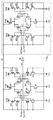
図1には、本発明に係る半導体集積回路装置に設けられる入力回路の一実施例の回路図が示されている。同図の各回路素子は、公知の半導体集積回路の製造技術によって、単結晶シリコンのような1個の半導体基板上において形成される。同図の回路は、NチャネルMOSFETとPチャネルMOSFETとからなるCMOS回路により構成され、PチャネルMOSFETは、そのバックゲート(チャネル)部に矢印を付すことによりNチャネルMOSFETと区別される。
【0008】
この実施例の入力回路は、前記レール・ツー・レール回路が利用される。すなわち、Pチャネル型の差動MOSFETQ1とQ2、その動作電流を形成するPチャネル型の電流源MOSFETQ3からなる第1増幅部と、Nチャネルの差動MOSFETQ4とQ5、その動作電流を流すNチャネル型の電流源MOSFETQ6により第2増幅部が構成される。上記Pチャネル型の電流源MOSFETQ3のソースは、電源電圧VDDQが与えられ、Nチャネル型の電流源MOSFETQ6のソースには、回路の接地電位VSSが与えられる。
【0009】
上記第1増幅部と第2増幅部の一方の差動MOSFETQ1とQ4のゲートは、第1入力端子INに接続される。上記第1増幅部と第2増幅部の他方の差動MOSFETQ2とQ5のゲートは、第2入力端子INBに接続される。これらの入力端子INとINBには、相補(非反転と反転)の入力信号が供給される。ここで、INBのBはバー(反転)信号であることを示している。
【0010】
上記第1差動部に対して、NチャネルMOSFETQ7〜Q10からなる第1出力部が設けられ、上記第2差動部に対してPチャネルMOSFETQ11〜Q14からなる第2出力部が設けられる。上記第1と第2出力部の一方である上記MOSFETQ7,Q8及びQ11,Q12が電源電圧VDDQと回路の接地電位VSSとの間には、カスコード(直列)形態に接続され、上記第1と第2出力部の他方である上記MOSFETQ9,Q10及びQ13,Q14が電源電圧VDDQと回路の接地電位VSSとの間には、カスコード形態に接続される。
【0011】
上記第1増幅部の差動MOSFETQ1とQ2のドレイン電流は、上記第1出力部のMOSFETQ8、Q10に流れるようにされる。同様に、第2増幅部の差動MOSFETQ4,Q5のドレイン電流は、上記第2出力部のMOSFETQ12,Q14に流れるようにされる。上記第1出力部の一方のMOSFETQ7と、第2出力部の一方のMOSFETQ11は、いわばソース入力、ゲート接地型の増幅MOSFETとして動作し、ドレインが第1出力端子に接続される。同様に、上記第1出力部の他方のMOSFETQ9と、第2出力部の一方のMOSFETQ13も、上記同様に増幅MOSFETとして動作してドレインが第2出力端子に接続される。このような一対の出力端子のうち、特に制限されないが、第1出力端子の信号outが出力増幅回路OAに伝えられて、CMOSレベルの内部信号とされる。第2出力端子の信号を出力増幅回路に伝えてCMOSレベルの内部信号とすることもできる。
【0012】
上記第2と第4の差動MOSFETの基板をソースに接続することで第2と第4の差動MOSFETのNBT劣化を防ぐことができる。
【0013】
上記第1増幅部,第2増幅部の電流源MOSFETQ3とQ6、及び上記第1出力部と第2出力部のMOSFETQ7〜Q14のゲートには、バイアス電圧VBが共通に接続される。このように、電流源MOSFETQ3、Q6及び及び上記第1出力部と第2出力部のMOSFETQ7〜Q14のゲート共通のバイアス電圧を供給する構成は、前記図14に示した自己バイアス型のレール・ツー・レール回路と同様である。
【0014】
この実施例では、前記図14のように増幅回路において自身がバイアス電圧BIASを形成する構成では、入力端子IN,INBの信号変化に対して負帰還がかかり、出力信号の変化速度が遅くなってしまうという問題を有する。つまり、本願発明にかかる半導体集積回路装置のように、高速で低振幅の入力信号を受ける入力回路には不向きなものとなる。
【0015】
この実施例では、上記バイアス電圧VBが専用のバイアス回路VBGにより形成される。バイアス回路VBGは、上記入力回路と同じ回路により構成される。つまり、Pチャネル型の差動MOSFETQ21とQ22、その動作電流を形成するPチャネル型の電流源MOSFETQ23からなる第3増幅部と、Nチャネルの差動MOSFETQ24とQ25、その動作電流を流すNチャネル型の電流源MOSFETQ26により第4増幅部が構成される。
【0016】
上記Pチャネル型の電流源MOSFETQ23のソースは、電源電圧VDDQが与えられ、Nチャネル型の電流源MOSFETQ6のソースには、回路の接地電位VSSが与えられる。上記第1増幅部と第2増幅部の一方の差動MOSFETQ1とQ4のゲートは、上記第1入力端子INに接続される。上記第1増幅部と第2増幅部の他方の差動MOSFETQ2とQ5のゲートは、上記第2入力端子INBに接続される。
【0017】
上記第3差動部に対して、NチャネルMOSFETQ27〜Q30からなる第3出力部が設けられ、上記第4差動部に対してPチャネルMOSFETQ31〜Q34からなる第4出力部が設けられる。上記第3と第4出力部の一方である上記MOSFETQ27,Q28及びQ31,Q32が電源電圧VDDQと回路の接地電位VSSとの間にカスコード形態に接続され、上記第1と第2出力部の他方である上記MOSFETQ29,Q30及びQ33,Q34が電源電圧VDDQと回路の接地電位VSSとの間にカスコード形態に接続される。
【0018】
上記第3増幅部の差動MOSFETQ21とQ22のドレイン電流は、上記第3出力部のMOSFETQ28、Q30に流れるようにされる。同様に、第4増幅部の差動MOSFETQ24,Q25のドレイン電流は、上記第4出力部のMOSFETQ32,Q34に流れるようにされる。上記第3出力部の一方のMOSFETQ27と、第4出力部の一方のMOSFETQ31のドレインは第3出力端子に接続される。同様に、上記第1出力部の他方のMOSFETQ29と、第2出力部の他方のMOSFETQ33も、上記同様にドレインが第4出力端子に接続される。このような一対の出力端子は、相互に接続されてバイアス電圧VBを形成する。
【0019】
つまり、相補の出力端子同士を接続して、入力端子INとINBに対応した出力信号のハイレベルとロウレベルの中間電圧を形成し、それをバイアス電圧VBとし、電流源MOSFETQ23とQ26のゲートと、上記MOSFETQ27〜Q34のゲートに供給される。
【0020】
上記バイアス回路VBGに対しても、入力端子INとINBに対応した相補の入力信号が形成され、かかる入力信号に対応した相補の出力信号を形成する出力端子同士を相互に接続することにより、相補出力信号が一致するように電流源MOSFETQ23、Q26及びカスコード部のMOSFETQ27〜Q34のゲートに供給されるバイアス電圧VBを形成します。この電圧VBを入力回路を構成する上記電流源MOSFETQ3、Q6及びカスコード部のMOSFETQ7〜Q14のゲートに供給することにより、入力回路においては、入力端子INとINBに対応してハイレベル/ロウレベルに変化するような出力信号を形成する。そのうちの一方の出力信号outをCMOSインバータ回路等の出力増幅回路OAにより増幅してCMOSレベルの内部信号を形成することができる。
【0021】
入力回路においては、出力信号のレベルを決める信号伝達動作において、上記バイアス電圧VBを形成するための負帰還動作を行わないから、入力端子INとINBから入力された入力信号に対応した出力信号outを形成する信号伝達動作を高速に行うようにすることができる。
【0022】
図2には、本発明に係る半導体集積回路装置に設けられる入力回路の他の一実施例の回路図が示されている。この実施例の入力回路は、前記図1と同じ回路が用いられる。ただし、一対の入力端子のうちの一方の入力端子INには、入力信号が供給され、前記図1の入力回路では反転の入力信号が供給される入力端子INBに対応した入力端子は、上記入力信号のハイレベル/ロウレベルを判定する参照電圧VREFが供給される参照電圧端子とされる。
【0023】
このような参照電圧VREFを用いた入力回路に供給されるバイアス電圧VBを形成するバイアス回路VBGでは、一対の入力端子が共に参照電圧VREFが供給される参照電圧端子とされる。素子にバラツキがなければ、同じ参照電圧VREFが供給されるので、一対の出力信号も同じくなるはずであるが、実際には差動ペア素子でのオフセット、出力MOSFETでも同様なオフセットを持つので、かかるオセットを補償するようなバイアス電圧VBが形成され、それが上記入力回路の対応するMOSFETに供給される。これにより、シングル構成の入力回路においても、動作の高速化と安定化を実現することができる。
【0024】
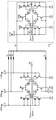
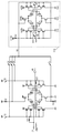
図3と図4には、本発明に係る半導体集積回路装置に設けられる入力回路の他の一実施例の回路図が示されている。この実施例の入力回路は、前記図1の実施例の改良に係るものであり、図1の実施例回路に対してスイッチS1〜S11が付加されて、図3、図4の実施例が構成される。このうち、図3には、半導体集積回路装置が通常の動作を行うノーマルモード時のスイッチS1〜S11の状態が示され、図4には、半導体集積回路装置が動作を行わないスタンバイモード時のスイッチS1〜S11の状態が示されている。
【0025】
図3、図4において、入力回路は、カスコード部が2つに分けられて、それぞれにスイッチS1、S4と、スイッチS3とS6が設けられる。また、Pチャネル型とNチャネル型の電流源MOSFETにもスイッチS2、S5と、スイッチS11とS7が設けられる。上記スイッチS1〜S3は、電源電圧VDDQに選択的に接続するために設けられ、スイッチS11は回路の接地電位VSSに選択的に接続するために設けられる。そして、スイッチS4〜S6は、バイアス回路VBGで形成されたバイアス電圧VBを選択的に伝えるために設けられる。バイアス回路VBGにおいても、カスコード部が2つに分けられて、それぞれにスイッチS8、S9が設けられて、それぞれの出力端子と選択的に接続される。2つのカスコード部のMOSFETの共通接続されたゲートに対して、電源電圧VDDQに選択的に接続するためのスイッチS10が設けられる。
【0026】
図3のノーマルモードでは、スイッチS1〜S3、S11はオフ状態にされ、スイッチS4〜S7はオン状態にされる。これにより、入力回路は、前記図1の入力回路と同じ接続構成とされる。バイアス回路VBGは、スイッチS8とS9がオン状態にされ、スイッチS10がオフ状態にされる。これにより、バイアス回路VBGは、前記図1のバイアス回路と同じ接続構成とされる。この結果、図1の実施例と同様に動作して、バイアス回路VBGは入力端子INとINBに対応したバイアス電圧VBを形成する。入力回路は上記バイアス回路で形成されたバイアス電圧VBにより動作し、入力端子INとINBから供給される入力信号に対応した信号outを形成する。
【0027】
図4のスタンバイモードでは、上記図3とは逆に、スイッチS1〜S3、S11はオン状態にされ、スイッチS4〜S7はオフ状態にされる。これにより、入力回路のカスコード部のMOSFETのゲートには、バイアス電圧VBに代えて電源電圧VDDQが供給されてPチャネルMOSFETがオフ状態にされ、Pチャネル電流源MOSFETには上記電源電圧VDDQが供給されてオフ状態にされ、Nチャネル電流源MOSFETには回路の接地電位VSSが供給されてオフ状態にされる。したがって、入力回路においては、電源電圧VDDQと回路の接地電位VSSとの間で電流経路が形成されないので低消費電力となる。
【0028】
バイアス回路VBGにおいても、前記図3と逆に、スイッチS8とS9がオフ状態にされ、スイッチS10がオン状態にされる。これにより、バイアス回路VBGは、PチャネルMOSFETが全てオフ状態にされるので、上記電源電圧VDDQによって、Nチャネル電流源MOSFETがオン状態となり、カスコード部のNチャネルMOSFETがオン状態となっても、電源電圧VDDQと回路の接地電位VSSとの間で電流経路が形成されないので低消費電力となる。このように、スタンバイモードでは、入力回路及びバイアス回路で直流電流が発生しないから低消費電力となる。ただし、オフ状態のPチャネルMOSFETに流れるリーク電流は無視するものとする。
【0029】
この実施例のように、スタンバイモードにおいて、カスコード部の各MOSFETに対して電源電圧VDDQを供給する構成は、PチャネルMOSFETをオフ状態にさせるものであり、PチャネルMOSFETをオン状態にさせるようにゲートと基板(チャネル間)に電圧を供給した場合に生じるNBTI(Negative Bias Temperature Instability)劣化を防止する上で効果的である。また、差動MOSFETの基板(チャネル)とソースとを接続する構成は、上記NBTI劣化を防止する上で有益である。このため、差動MOSFETは、それぞれが電気的に独立したウェル領域に形成される。
【0030】
図5には、本発明に係る半導体集積回路装置に設けられる入力回路の更に他の一実施例の回路図が示されている。この実施例の入力回路は、前記レール・ツー・レール回路と、CMOS回路との2通りの入力動作に切り換えることが可能な機能が付加される。前記図3(図4)の回路において、入力端子INと、出力信号を形成するカスコード部の各MOSFETのゲートとの間に、スイッチ12が設けられる。同様に、他方のカスコード部のMOSFETのゲートと、それに対応した入力端子INBとの間にスイッチ13が設けられる。
【0031】
同図には、CMOS入力モードの様子が示されており、スイッチS 1、S3はオフ状態にされ、スイッチS2とS11はオン状態にされる。他のスイッチS4〜S10の状態は、前記図4のスタンバイモードのときと同様であり、バイアス回路は回路動作が停止されて低消費電力状態になる。
【0032】
入力回路においては、2つの差動回路の電流源MOSFETがそれぞれオフ状態にされて差動回路には電流が流れなくされる。したがって、スイッチS12のオン状態により、入力端子INの入力信号は、カスコード接続のMOSFETのゲートに共通に供給される。この構成は、2つのPチャネルMOSFETと2つのNチャネルMOSFETとが直列接続されており、それらのゲートに入力信号が供給され、NチャネルMOSFETとPチャネルMOSFETのドレイン接続点から出力信号を得るので上記カスコード部は、CMOSインバータ回路と等価の動作を行うものとされる。
【0033】
入力端子INBからの入力信号も、スイッチS13を通して他方のカスコード接続のMOSFETのゲートに共通に供給される。それ故、かかるカスコード接続のMOSFETもCMOSインバータ回路と等価となって、その出力端子から出力信号を形成し、図示しない内部回路に取り込んだ入力信号を伝えることができる。なお、入力端子INの入力信号に対して、入力端子INBの入力信号が反転信号の場合には、わざわざ2つの入力回路(カスコード接続のMOSFET)を用いて、それぞれを入力する必要はない。例えば、バー信号の場合には、入力端子INBを用い、テュルー信号の場合には入力端子INを用いるようにいずれか一方を選択的に使用すればよい。
【0034】
上記のスイッチS1〜S13は、例えばMOSFETにより構成される。MOSFETの持つしきい値電圧により、入力された電圧がそのまま出力できない場合には、PチャネルMOSFETとNチャネルMOSFETを並列接続して、それらを制御信号に従ってオン/オフさせるようにするCMOSスイッチを用いるようにすればよい。
【0035】
図6には、本発明に係る半導体集積回路装置に設けられる入力回路の更に他の一実施例の回路図が示されている。この実施例は、前記図2の実施例と基本的には同じである。この実施例では、入力回路のPチャネル差動MOSFETQ1とQ2、カスコード部のPチャネルMOSFETQ11〜Q14は、そのチャネル幅がW4のように同一に形成される。また、入力回路のNチャネル差動MOSFETQ4とQ5、カスコード部のPチャネルMOSFETQ7〜Q10は、そのチャネル幅がW3のように同一に形成される。
【0036】
上記Pチャネル差動MOSFETQ1とQ2の動作電流を形成するPチャネルMOSFETQ3は、そのチャネル幅がW3のように同じPチャネルの前記他のMOSFETQ1、Q2等のチャネル幅W4よりも小さく形成され、言い換えるならば、オン抵抗値が大きく形成される。同様に、上記Nチャネル差動MOSFETQ4とQ5の動作電流を形成するPチャネルMOSFETQ6は、そのチャネル幅がW2のように同じNチャネルの前記他のMOSFETQ4、Q5等のチャネル幅W3よりも小さく形成され、言い換えるならば、オン抵抗値が大きく形成される。バイアス回路VBGにおいても、MOSFETQ21〜Q34は、対応する入力回路の前記MOSFETQ1〜Q14と同じくチャネル幅がW1〜W4のようにそれぞれ形成される。
【0037】
差動増幅部において、電流源MOSFETQ3(Q23)及びQ6(Q26)のオン抵抗値を大きくした理由は、それに対応した差動MOSFETQ1とQ2(Q21とQ22)のドレイン電位の変化を小さくするためである。つまり、Nチャネル差動MOSFETQ4とQ5においては、そのドレイン電位の低電圧側への落ち込みを制限し、Pチャネル差動MOSFETQ1とQ2においては、そのドレイン電位の浮き上がりを制限する。
【0038】
このような差動増幅部でのドレイン電位の変動を小さくすることにより、信号切り替わりを高速にするものである。つまり、一般的な差動回路のように差動MOSFETと、その動作電流を形成する電流源MOSFETを同じサイズとした場合には、そのオン抵抗値も同様となって、差動入力に対して相対的にオン状態にせされるMOSFETのドレイン電位の落ち込み又は浮き上がりが大きくなる。例えば、差動MOSFETQ4がオン状態に、MOSFETQ5がオフ状態のときに上記MOSFETQ4のドレイン電圧の落ち込みが大きいと、入力信号が変化して出力レベルの切り換えを行うとき、上記ドレイン電圧の落ち込みはカスコード部の電流源MOSFETQ12でしか回復させることができなく、このMOSFETQ12はカスコード部の増幅MOSFETQ11へも電流を供給するので上記ドレイン電圧の落ち込みの回復に時間がかかってしまう。
【0039】
つまり、差動MOSFETQ4がオン状態からオフ状態に切り換えられ、MOSFETQ12の電流は増幅MOSFETQ11に供給されて、上記差動MOSFETQ4がオン状態のときの反転信号を形成する動作を行わなければならないのに、上記MOSFETQ4のドレインの寄生容量を充電するためにも使われることとなって出力の切り換えを遅くしてしまう。
【0040】
これに対して、本願発明のように差動MOSFETQ1とQ2(Q4とQ5)に対して、電流源MOSFETQ3(Q6)のオン抵抗値を大きくするという単純な構成により、上記差動MOSFETQ1とQ2(Q4とQ5)のドレイン電圧の変化幅を小さくでき、結果として上記のような出力切り換えを高速に行うことが可能となる。つまり、入力信号の伝達速度を高速に行うようにすることができる。
【0041】
この実施例のように、入力回路とバイアス回路とにおいて、対応するMOSFETのサイズをW1〜W4のように互いに等しくした場合を基準にし、入力回路側の各MOSFETのサイズを(W1〜W4)×4のようにそれぞれを4倍にすると、各MOSFETに流れる電流も4倍となり、信号伝達速度を高速にすることができる。この場合には、入力回路側のみに大きな電流が流れ、バイアス回路は少なくてよいのでノーマルモードでの効率的に電流を使用することができる。
【0042】
また、入力回路とバイアス回路とにおいて、対応するMOSFETのサイズをW1〜W4のように互いに等しくした場合を基準にし、入力回路側の各MOSFETのサイズを(W1〜W4)×8のようにそれぞれを8倍にすると、各MOSFETに流れる電流も8倍となり、いっそうの信号伝達速度を高速にすることができる。この場合には、入力回路側のみに大きな電流が流れ、バイアス回路は少なくてよいのでノーマルモードでの効率的に電流を使用することができる。
【0043】
例えば、後述するようなシンクロナスSRAMにおいて、クロック信号CLK,CLKBを入力する入力回路には、前記(W1〜W4)×8のようなMOSFETを用い、制御信号S,WE,WEx等は前記(W1〜W4)×4のようなMOSFETを用い、アドレス信号A0〜A18・ASやDQ0〜DA35は、(W1〜W4)×1のようにバイアス回路VBGと等倍にするよう、それぞれの入力信号の要求される伝達速度に対応した3段階の使い分けに利用できる。
【0044】
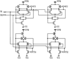
図7には、本発明に係る半導体集積回路装置に設けられる入力回路の更に他の一実施例の回路図が示されている。この実施例は、前記のようなレール・ツー・レール回路ではなく、Nチャネル差動MOSFET、Nチャネル電流源MOSFET及びPチャネル負荷MOSFETにより第1差動増幅回路を構成し、同様にPチャネル差動MOSFET、Pチャネル電流源MOSFET及びNチャネル負荷MOSFETにより第2差動増幅回路を構成し、上記第1と第2の差動増幅回路の入力端子を共通にして入力端子CK,CKBに接続する。
【0045】
特に制限されないが、電流源MOSFETと差動MOSFETの共通ソースとの間には、差動MOSFETのドレイン出力をそれぞれのゲートに受け、並列形態にされた2つのMOSFETが設けられる。これらのMOSFETは、出力信号の変動を小さくするような負帰還動作を行うために設けられる。
【0046】
上記第1及び第2差動増幅回路のそれぞれに対して、それぞれ同様な第3及び第4差動増幅回路が設けられ、Nチャネル差動MOSFETを持つ第1と第3差動増幅回路とが縦列形態に接続され、Pチャネル差動MOSFETを持つ第2と第4差動増幅回路とが縦列形態に接続されて、それぞれにおいて2段増幅動作を行うようにされる。
【0047】
そして、第3増幅回路の出力信号はPチャネルの出力MOSFETのゲートに供給され、第4増幅回路の出力信号はNチャネルの出力MOSFETのゲートに供給され、上記Pチャネル出力MOSFETとNチャネル出力MOSFETとの相補の増幅信号の対応するもの同士が直列形態に接続されて反転出力信号XBと非反転出力信号XTを形成する。これらの出力信号XBとXTは、CMOSインバータ回路を通して相補信号として内部回路に取り込まれる。
【0048】
上記第1ないし第4差動増幅回路のそれぞれは、電流源MOSFETのゲートに供給されるバイアス電圧と、それと反対導電型の負荷MOSFETのゲートに供給されるバイアス電圧とが同電位にされる。これらのバイアス電圧は、次に説明するようなバイアス回路により形成される。
【0049】
図8には、図7の入力回路に用いられるバイアス回路の一実施例の回路図が示されている。バイアス回路は、前記図7の第1ないし第4差動増幅回路の電流源MOSFETと負荷MOSFETに供給される4通りのバイアス電圧NB1、PB1、NB2,PB2を形成する。
【0050】
バイアス回路は、前記レール・ツー・レール回路に設けられたバイアス回路と同様に、入力回路と同じ回路構成のものが用いられる。つまり、前記図7の入力回路の第1ないし第4差動増幅回路と同じ回路構成にされた4つの差動増幅回路が用いられる。前段の2つの差動増幅回路には、それぞれ入力回路と同じく入力端子CKとCKBに接続される。前段の差動増幅回路の差動出力が後段の差動増幅回路の入力端子に接続されるまでは前記入力回路と同様である。
【0051】
上記バイアス回路を構成する4つの差動増幅回路は、それぞれの差動MOSFETのドレイン出力が共通に接続される。上記4つの差動増幅回路のそれぞれにおいては、相補の出力端子を相互に接続して等しい電圧になるように、自身の負荷MOSFET及び電流源MOSFETを制御しつつ、4通りのバイアス電圧NB1、NB2、PB1、PB2を形成する。これにより、Nチャネル差動MOSFETと、Pチャネル差動MOSFETを用いて、電源電圧と回路の接地電位の範囲内で変化する入力信号に応答できる入力回路の動作の高速化と安定化を実現することができる。
【0052】
図9には、この発明に用いられるPチャネルMOSFETの一実施例の素子構造図が示されている。図9(A)には平面構造が、図9(B)には断面構造が示されている。PチャネルMOSFETは、N型ウェルNWELにおいて、基板上に薄いゲート絶縁膜を介して形成されたゲート電極FGを挟むようにソース,ドレインを構成するP+型半導体領域Lが形成される。NウェルNWELには、ウェルバイアス電圧を供給するためにN+半導体領域が設けられる。ここで、前記図6で示したゲート幅Wは、ゲート,ソース及びドレインが平行に並ぶ方向のソース,ドレイン拡散層の長さをいう。また、ゲート長Lgは、チャル電流が流れる長さであり、ソース,ドレインの間隔に対応している。
【0053】
図10には、この発明に用いられるNチャネルMOSFETの一実施例の素子構造図が示されている。図10(A)には平面構造が、図10(B)には断面構造が示されている。NチャネルMOSFETは、P型ウェルNWELにおいて、薄いゲート絶縁膜を介して形成されたゲート電極FGを挟むようにソース,ドレインを構成するN+型半導体領域Lが形成される。PウェルPWELには、ウェルバイアス電圧を供給するためにP+半導体領域が設けられる。ゲート幅Wとゲート長Lgは、上記図9と同様である。
【0054】
図11には、この発明が適用されるシンクロナスSRAM(以下、単にSSRMという)の一実施例のブロック図が示されている。この実施例のシンクロナスSRAMは、公知のCMOS集積回路の製造技術により、単結晶シリコンのような1つの半導体基板上において形成される。
【0055】
この実施例のSSRAMは、アドレス端子A0〜A18とウェイセレクト用アドレスASからなる20ビットによって約1M(メガ)のアドレス空間を持つ。データ端子DQ0〜DQ35により36ビットずつパラレルに読み出しと書き込みが行われるから、メモリアレイMARYには約36Mビットの記憶容量をもつようにされる。メモリアレイMARYは、スタティック型メモリセルがワード線と相補のビット線との交点にマトリクス配置されて構成される。
【0056】
上記アドレス端子A0〜A18のアドレス信号は、アドレスバッファADBを通してアドレスレジスタAG1に取り込まれる。非反転と反転からなる相補のクロック信号CLK、CLKBはクロックバッファCKBを通して取り込まれる。そして、リード/ライト制御のための制御信号S,WE,WExはコントロールバッファCOBを通して取り込まれる。また前記セレクト信号ASもアドレスバッファADBを通してアドレスレジスタAG2に取り込まれる。データ端子DQ0〜DQ35からの書き込みデータに対応して入力バッファIBが設けられる。
【0057】
したがって、前記実施例の入力回路はこれら各種入力回路に適用される。特に、前記図6の実施例において、アドレスバッファADBやデータ入力バッファIBは、図6の実施例回路が用いられ、コントロールバッファCOBは、バイアス回路の対応するMOSFETに対してゲート幅Wが4倍にされたMOSFETにより入力回路が構成される。更に、最高速が要求されるクロックバッファCKBは、バイアス回路に対してゲート幅Wが8倍にされたMOSFETにより入力回路が構成される。
【0058】
アドレスレジスタAG1は、読み出し動作のときにはセレクタSELAによりメモリアレイMARYのデコーダに伝えられる。書き込み動作のときには、書き込みアドレスレジスタWAR11、WAR21によって時間調整が行われてセレクタを通して上記デコーダに伝えられる。同様に、ウェイセレクト用のアドレスASも、同様なレジスタWAR12、WAR22によって時間調整が行われる。書き込み動作では、書き込みアドレスとそれに対応した書き込みデータとに1サイクルのずれがあるので、上記書き込みアドレスレジスタによってその調整が行われる。
【0059】
特に制限されないが、メモリアレイMARYは、上記アドレス信号A0〜A18によって、36×2=72ビット分のデータがウェイ0(SA0)とウェイ1(SA1)によって読み出される。書き込みデータは、データレジスタDRG1,DRG2を通してメモリアレイMARYのライトアンプWA0,WA1に伝えられる。上記センスアンプSA0,SA1の読み出しデータと、データレジスタDRG2の書き込みデータとは、セレクタにより選択され、さらにその出力とデータレジスタDRG1の書き込みデータとがセレクタにより選択された出力レジスタOR0,OR1に伝えられる。
【0060】
上記セレクタの選択信号は、選択制御回路SLGにより形成される。この2つの出力レジスタOR0とOR1に伝えられたデータのうち、一方が上記ウェイアドレスASに対応したウェイセレクト信号WSELにより選択されて、出力バッファOBを通して出力される。選択制御回路SLGは、書き込みアドレスレジスタWAR11、WAR21の書き込みアドレスと、入力されたアドレスとを比較するコンパレータCMP1,CMP2の信号と、上記書き込みアドレスレジスタWAR12、WAR22のウェイセレクト用アドレスとを参照して上記選択信号を形成する。
【0061】
図12には、図11のSSRAMの動作の一例を説明するためのタイミング図が示されている。セレクト信号SBのロウレベル(論理0)と、ライトイネーブル信号WEBのハイレベル(論理1)によりリードサイクルとされ、アドレス信号A0−A18によりアドレスA0が取り込まれて前記2ウェイ分のデータが読み出される。第2サイクルで同様にリードサイクルとされ、アドレス信号A0−A18によりアドレスA1が取り込まれ前記2ウェイ分のメモリセルの選択動作が行われる。1サイクル遅れてウェイアドレスASのロウレベル(論理0)が入力されてウェイ0が指定されると、データレジスタDR0に取り込まれているウェイ0に対応したデータQ00が出力される。第3サイクルでセレクト信号SBのハイレベル(論理1)とすると、そのサイクルは非選択サイクルとされるが、そのときにウェイアドレスASのハイレベル(論理1)が入力されて、前記アドレスA1に対応して読み出されているウェイ1に対応したデータQ11が出力される。
【0062】
第5サイクル目で、セレクト信号SBのロウレベル(論理0)と、ライトイネーブル信号WEBのロウレベル(論理0)によりライトサイクルとされ、アドレス信号A0−A18によりアドレスA2とウェイアドレスASのロウレベル(論理0)が取り込まれる。第6サイクル目で同様にライトサイクルとされ、アドレス信号A0−A18によりアドレスA3とそれに対応したウェイアドレスASのハイレベル(論理1)が取り込まれ、上記アドレスA2とウェイアドレスの0に対応した書き込みデータD20が入力される。上記ライトサイクルの間にもリードサイクルの挿入が可能とされ、その調整のためにアドレスレジスタ、ライトデータレジスタ、コンパレータ等が用いられる。
【0063】
このようなSSRAMにおいて、メモリセル等は最小加工寸法によりMOSFETのゲート長Lgが形成される。例えば、0.12μmプロセスの加工寸法によりメモリセルを構成するMOSFETが形成される場合、前記入力回路(バイアス回路)のMOSFETの寸法は、それよりも大きく形成される。この理由は、上記のような最小加工寸法で形成した場合に、ゲート長Lgのバラツキによる影響が大きくしきい値電圧の変動幅も大きくなる。
【0064】
例えば、図1において入力回路の差動MOSFETQ1,Q2(Q4,Q6)、電流源MOSFETQ3(Q6)及び負荷MOSFETQ8,Q10(Q12,Q14)は、ゲート長Lgを最小加工寸法の約2倍の0.25μmのように大きく形成される。そして、カスケード部のMOSFETのうち、上記負荷(電流源)としてのMOSFETQ8,Q10(Q12,Q14)は上記のように大きく形成されるが、増幅用のMOSFETQ7,Q9(Q11,Q13)はゲート長Lgが0.16μmのように小さく形成される。
【0065】
上記MOSFETQ7,Q9(Q11,Q13)のゲート長Lgを小さくすることにより、そのゲート容量、つまりはゲート電極とチャネル間の容量を小さくすることができる。これにより、カスコード部の出力信号経路における寄生容量が小さくなり、寄生容量の充放電によって形成される出力信号電圧outの変化を高速にすることができる。
【0066】
差動増幅回路においては、前記のように差動MOSFETと電流源MOSFETのチャネル長Lgは等しく形成されるが、図6の実施例のように差動MOSFETQ1とQ2(Q4とQ5)のゲート幅W4(W3)に対して、電流源MOSFETQ3(Q6)のゲート幅W1(W2)のように小さく形成される。これにより、前記のように差動MOSFETのドレイン電圧の変化幅を小さくでき、伝達信号の切り換えを高速に行うようにすることができるものである。
【0067】
SSRAMにおいて、例えば動作電源電圧VDDQを1.2Vのように低い電圧まで動作可能にする場合、入力回路やバイアス回路のMOSFETは0.4Vのような低しきい値電圧に形成される。このような低しきい値電圧にするために、図9、図10の素子構造において、イオン打ち込み技術等によるゲート電極FG下の半導体基板表面にウェルと反対導電型の不純物の導入制御によって設定される。
【0068】
上記のようなMOSFETのサイズのゲート長Lg、ゲート幅W設定は、前記実施例のレール・ツー・レール回路の他に、前記図13や図14の示されたレール・ツー・レール回路にも適用することによって、高速化や動作の安定化を図るようにすることができる。
【0069】
SSRAMにおいて、CMOSレベルの入力信号を受ける論理回路等においては、MOSFETのオフ状態でのリーク電流又はスレッショルドリーク電流を低減させるために、そのしきい値電圧は前記入力回路、バイアス回路のMOSFETよりも大きく、例えば0.6V程度の高しきい値電圧に設定される。このように、半導体集積回路装置において2種類のしきい値電圧を持つMOSFETを形成する場合、イオン打ち込み技術等によるゲート電極FG下の半導体基板表面の不純物の制御によって設定される。
【0070】
以上本発明者よりなされた発明を実施例に基づき具体的に説明したが、本願発明は前記実施例に限定されるものではなく、その要旨を逸脱しない範囲で種々変更可能であることはいうまでもない。例えば、図2の実施例において、各入力回路のそれぞれに対してバイアス回路を設けるもの他、1つの入力回路に代表させてバイアス回路を動作させ、それにより形成されたバイアス電圧を複数の入力回路に供給する構成としてもよい。個々の入力回路に一対一に対応してバイアス回路を設ける構成は、それに供給される入力信号に対応した最適なバイアス電圧を形成することができる反面、回路規模が大きくなる。これに対して、図2のように参照電圧VREFは全入力回路において共通であるので、1つのバイアス回路で代表させて複数の入力回路に供給する構成は、回路が簡素化できる。
【0071】
この発明は、入力信号の周波数が約1GHzを超え、内部回路がCMOS構成の半導体集積回路装置に有益なものとなる。入力信号の周波数が約1GHzを超えるようになると、容量反射で入力信号の振幅が小さくなり、データ有効時間も小さくなり、入力電位の中心がずれてくる傾向にあるので、かかる入力信号を受ける入力回路として前記実施例の入力回路は好適なものとなる。あるいは、入力信号振幅がCMOS振幅よりも小さい、内部回路がCMOS回路により構成される各種半導体集積回路装置に適用して好適なものとなる。
【0072】
【発明の効果】
本願において開示される発明のうち代表的なものによって得られる効果を簡単に説明すれば、下記の通りである。一対の第1入力端子にそれぞれゲートが接続された第1導電型の第1差動MOSFET対及びその共通ソースに設けられて動作電流を形成する第1導電型の第1電流源MOSFETを第1増幅部とし、上記一対の第1入力端子にそれぞれゲートが接続された第2導電型の第2差動MOSFET対及びその共通ソースに設けられて動作電流を形成する第2導電型の第2電流源MOSFETを第2増幅部とし、上記第1差動MOSFET対に流れる電流を供給する第2導電型の第1MOSFET対を含む第1出力部、上記第2差動MOSFET対に流れる電流を供給する第1導電型の第2MOSFET対を含む第2出力部を設けて増幅回路を構成し、かかる増幅回路と同様な回路を用イテバイアス回路を構成し、その一対の出力端子を共通接続して中点に対応した電圧を形成し、かかる電圧を上記増幅回路の第1ないし2電流源MOSFETのゲート及び第1ないし第2MOSFETのゲート及びバイアス回路の対応する電流源MOSFET及びMOSFETのゲートに供給することにより、電源電圧と回路の接地電位の範囲内で変化する入力信号に応答できる入力回路の動作の高速化と安定化を実現することができる。
【図面の簡単な説明】
【図1】本発明に係る半導体集積回路装置に設けられる入力回路の一実施例を示す回路図である。
【図2】本発明に係る半導体集積回路装置に設けられる入力回路の他の一実施例を示す回路図である。
【図3】本発明に係る半導体集積回路装置に設けられる入力回路の他の一実施例を示す回路図である。
【図4】本発明に係る半導体集積回路装置に設けられる入力回路の他の一実施例を示す回路図である。
【図5】本発明に係る半導体集積回路装置に設けられる入力回路の更に他の一実施例を示す回路図である。
【図6】本発明に係る半導体集積回路装置に設けられる入力回路の更に他の一実施例を示す回路図である。
【図7】本発明に係る半導体集積回路装置に設けられる入力回路の更に他の一実施例を示す回路図である。
【図8】図7の入力回路に用いられるバイアス回路の一実施例を示す回路図である。
【図9】この発明に用いられるPチャネルMOSFETの一実施例を示す素子構造図である。
【図10】この発明に用いられるNチャネルMOSFETの一実施例を示す素子構造図である。
【図11】この発明が適用されるSSRAMの一実施例を示すブロック図である。
【図12】図11のSSRAMの動作の一例を説明するためのタイミング図である。
【図13】この発明に先立って検討されたレール・ツー・レール回路の回路図である。
【図14】従来の自己バイアス型のレール・ツー・レール回路の回路図である。
【符号の説明】
Q1〜Q34…MOSFET、IN,INB…入力端子、OA…出力増幅回路、VBG…バイアス回路、
PWEL…P型ウェル、NWEL…N型ウェル、NISO…分離領域、FG…ゲート電極、Psub…P型基板、
S1〜S13…スイッチ、AG1,AG2…アドレスレジスタ、WAR11〜WAR22…書き込みアドレスレジスタ、SEL…セレクタ、MARY…メモリアレイ、SLG…選択制御回路、CMP1,CMP2…コンパレータ、DRG1,DRG2…データレジスタ、OR0,OR1…出力レジスタ、IB…入力バッファ、OB…出力バッファ、ADB…アドレスバッファ、COB…コントロールバッファ、CKB…クロックバッファ。[0001]
BACKGROUND OF THE INVENTION
The present invention relates to a semiconductor integrated circuit device, and relates to a technique that is effective when used for an input circuit of a semiconductor integrated circuit device to which a small amplitude input signal is supplied.
[0002]
[Prior art]
Generally, a differential input circuit is used for an input circuit that receives an input signal with a small amplitude and needs to operate at high speed. However, when the input voltage Vin becomes low such that Vin <2 × Vth (the threshold voltage of the differential MOSFET and the current source MOSFET), the current of the current source MOSFET provided in the common source of the differential MOSFET decreases, There is a problem that normal operation cannot be performed.
[0003]
[Problems to be solved by the invention]
The inventor of the present application focuses on a rail-to-rail circuit (rail to rail is a registered trademark of Motorola, Inc.) that can operate even when the input signal is shifted to the power supply voltage or the ground potential of the circuit. did. FIG. 13 shows a circuit diagram of a rail-to-rail circuit studied prior to the present invention. This circuit requires biases P1, P2, N1, N2 and DCP, DCN, and takes into account the process variation of the elements, for example, the variation in the mutual conductance ratio between the P-channel MOSFET and the N-channel MOSFET, and the shift of the input voltage Vin. Difficult to use as a small amplitude, high speed input circuit.
[0004]
FIG. 14 shows a circuit diagram of a self-biased rail-to-rail circuit proposed by US Pat. No. 4,958,133. In addition, an example of using a rail-to-rail circuit for an operational amplifier is shown in a magazine “Transistor Technology”, page 201, March 2001 issue. Even though these circuits can be used as operational amplifiers, their signal transmission speed is low, so they are used for static RAM (random access memory) address signals, clock signals, and various control signals that require high-speed operation. It is not suitable as an input circuit for inputting.
[0005]
An object of the present invention is to provide a semiconductor integrated circuit device including an input circuit that can stably operate at a high speed up to a low voltage. The above and other objects and novel features of the present invention will be apparent from the description of this specification and the accompanying drawings.
[0006]
[Means for Solving the Problems]
The outline of a typical invention among the inventions disclosed in the present application will be briefly described as follows. A first amplifying unit includes a first conductivity type first differential MOSFET pair having a gate connected to each of the first input terminals and a first conductivity type first current source MOSFET provided at a common source thereof to generate an operating current. A second conductivity type second differential MOSFET whose gate is connected to the pair of first input terminals, respectively, and a second conductivity type second current source MOSFET which is provided at the common source and generates an operating current. As a second amplifying unit, a first output unit including a first MOSFET pair of a second conductivity type that supplies a current flowing through the first differential MOSFET pair, and a first output unit that supplies a current flowing through the second differential MOSFET pair An amplifier circuit is configured by providing a second output unit including a second pair of conductive MOSFETs, a bias circuit is configured using a circuit similar to the amplifier circuit, and the pair of output terminals are connected in common. To form a corresponding bias voltage is supplied to the corresponding current source MOSFET and the MOSFET gates and the bias circuit of the gate and the first to 2MOSFET the first to second current source MOSFET of the amplifier circuit.
[0007]
DETAILED DESCRIPTION OF THE INVENTION
FIG. 1 is a circuit diagram showing one embodiment of an input circuit provided in a semiconductor integrated circuit device according to the present invention. Each circuit element in the figure is formed on one semiconductor substrate such as single crystal silicon by a known semiconductor integrated circuit manufacturing technique. The circuit shown in the figure is constituted by a CMOS circuit composed of an N-channel MOSFET and a P-channel MOSFET, and the P-channel MOSFET is distinguished from the N-channel MOSFET by attaching an arrow to its back gate (channel) portion.
[0008]
The input circuit of this embodiment has the above-mentioned record. - Le Two Les - Circuit is used. That is, P-channel type differential MOSFETs Q1 and Q2, a first amplifying unit composed of a P-channel type current source MOSFET Q3 that forms an operating current thereof, N-channel differential MOSFETs Q4 and Q5, and an N-channel type that flows the operating current The current amplifier MOSFET Q6 constitutes a second amplifying unit. The source of the P-channel type current source MOSFET Q3 is supplied with the power supply voltage VDDQ, and the source of the N-channel type current source MOSFET Q6 is supplied with the circuit ground potential VSS.
[0009]
The gates of one of the differential MOSFETs Q1 and Q4 of the first amplifying unit and the second amplifying unit are connected to the first input terminal IN. The gates of the other differential MOSFETs Q2 and Q5 of the first amplifying unit and the second amplifying unit are connected to the second input terminal INB. These input terminals IN and INB are supplied with complementary (non-inverted and inverted) input signals. Here, B of INB indicates a bar (inverted) signal.
[0010]
A first output unit composed of N-channel MOSFETs Q7 to Q10 is provided for the first differential unit, and a second output unit composed of P-channel MOSFETs Q11 to Q14 is provided for the second differential unit. The MOSFETs Q7, Q8 and Q11, Q12, which are one of the first and second output units, are connected in a cascode (series) form between the power supply voltage VDDQ and the ground potential VSS of the circuit, and the first and second outputs The MOSFETs Q9, Q10 and Q13, Q14 which are the other of the two output units are connected in a cascode form between the power supply voltage VDDQ and the circuit ground potential VSS.
[0011]
The drain currents of the differential MOSFETs Q1 and Q2 of the first amplifier section are caused to flow through the MOSFETs Q8 and Q10 of the first output section. Similarly, the drain currents of the differential MOSFETs Q4 and Q5 of the second amplifying unit flow through the MOSFETs Q12 and Q14 of the second output unit. One MOSFET Q7 of the first output section and one MOSFET Q11 of the second output section operate as a so-called source-input, grounded-gate amplification MOSFET, and the drain is connected to the first output terminal. Similarly, the other MOSFET Q9 of the first output section and the one MOSFET Q13 of the second output section operate as amplification MOSFETs similarly to the above, and their drains are connected to the second output terminal. Of the pair of output terminals, although not particularly limited, the signal out of the first output terminal is transmitted to the output amplifier circuit OA to be a CMOS level internal signal. The signal of the second output terminal can be transmitted to the output amplifier circuit to be a CMOS level internal signal.
[0012]
NBT deterioration of the second and fourth differential MOSFETs can be prevented by connecting the substrates of the second and fourth differential MOSFETs to the sources.
[0013]
A bias voltage VB is commonly connected to the gates of the current source MOSFETs Q3 and Q6 of the first amplification unit and the second amplification unit, and the MOSFETs Q7 to Q14 of the first output unit and the second output unit. As described above, the configuration for supplying the bias voltage common to the gates of the current source MOSFETs Q3 and Q6 and the MOSFETs Q7 to Q14 of the first output unit and the second output unit is the self-bias type regulator shown in FIG. - Le Two Les - This is the same as the circuit.
[0014]
In this embodiment, when the amplifier circuit itself forms the bias voltage BIAS in the amplifier circuit as shown in FIG. 14, negative feedback is applied to the signal change of the input terminals IN and INB, and the change rate of the output signal becomes slow. Have the problem of That is, the semiconductor integrated circuit device according to the present invention is not suitable for an input circuit that receives a high-speed, low-amplitude input signal.
[0015]
In this embodiment, the bias voltage VB is formed by a dedicated bias circuit VBG. The bias circuit VBG is configured by the same circuit as the input circuit. In other words, P-channel type differential MOSFETs Q21 and Q22, a third amplifying unit comprising a P-channel type current source MOSFET Q23 that forms the operating current, N-channel differential MOSFETs Q24 and Q25, and an N-channel type that supplies the operating current. The fourth amplifying unit is configured by the current source MOSFET Q26.
[0016]
The source of the P-channel type current source MOSFET Q23 is supplied with the power supply voltage VDDQ, and the source of the N-channel type current source MOSFET Q6 is supplied with the circuit ground potential VSS. The gates of one of the differential MOSFETs Q1 and Q4 of the first amplifying unit and the second amplifying unit are connected to the first input terminal IN. The gates of the other differential MOSFETs Q2 and Q5 of the first amplifying unit and the second amplifying unit are connected to the second input terminal INB.
[0017]
A third output unit including N-channel MOSFETs Q27 to Q30 is provided for the third differential unit, and a fourth output unit including P-channel MOSFETs Q31 to Q34 is provided for the fourth differential unit. The MOSFETs Q27, Q28 and Q31, Q32, which are one of the third and fourth output units, are connected in a cascode form between the power supply voltage VDDQ and the circuit ground potential VSS, and the other of the first and second output units The MOSFETs Q29, Q30 and Q33, Q34 are connected in a cascode form between the power supply voltage VDDQ and the circuit ground potential VSS.
[0018]
The drain currents of the differential MOSFETs Q21 and Q22 of the third amplifying unit are caused to flow through the MOSFETs Q28 and Q30 of the third output unit. Similarly, the drain currents of the differential MOSFETs Q24 and Q25 of the fourth amplifier section are caused to flow through the MOSFETs Q32 and Q34 of the fourth output section. One MOSFET Q27 of the third output section and the drain of one MOSFET Q31 of the fourth output section are connected to a third output terminal. Similarly, the drains of the other MOSFET Q29 of the first output unit and the other MOSFET Q33 of the second output unit are connected to the fourth output terminal in the same manner as described above. Such a pair of output terminals are connected to each other to form a bias voltage VB.
[0019]
That is, the complementary output terminals are connected to form an intermediate voltage between the high level and the low level of the output signal corresponding to the input terminals IN and INB, which is set as the bias voltage VB, and the gates of the current source MOSFETs Q23 and Q26; It is supplied to the gates of the MOSFETs Q27 to Q34.
[0020]
Complementary input signals corresponding to the input terminals IN and INB are also formed for the bias circuit VBG, and complementary output signals that form complementary output signals corresponding to the input signals are connected to each other. The bias voltage VB supplied to the gates of the current source MOSFETs Q23 and Q26 and the MOSFETs Q27 to Q34 in the cascode part is formed so that the output signals match. By supplying this voltage VB to the gates of the current source MOSFETs Q3 and Q6 and the cascode MOSFETs Q7 to Q14 constituting the input circuit, the input circuit changes to a high level / low level corresponding to the input terminals IN and INB. An output signal is generated. One of the output signals out can be amplified by an output amplifier circuit OA such as a CMOS inverter circuit to form a CMOS level internal signal.
[0021]
In the input circuit, since the negative feedback operation for forming the bias voltage VB is not performed in the signal transmission operation for determining the level of the output signal, the output signal out corresponding to the input signals input from the input terminals IN and INB. Can be performed at high speed.
[0022]
FIG. 2 is a circuit diagram showing another embodiment of the input circuit provided in the semiconductor integrated circuit device according to the present invention. As the input circuit of this embodiment, the same circuit as that shown in FIG. 1 is used. However, an input signal is supplied to one input terminal IN of the pair of input terminals, and the input terminal corresponding to the input terminal INB to which an inverted input signal is supplied in the input circuit of FIG. The reference voltage terminal is supplied with a reference voltage VREF for determining the high level / low level of the signal.
[0023]
In the bias circuit VBG that forms the bias voltage VB supplied to the input circuit using the reference voltage VREF, both the pair of input terminals are used as reference voltage terminals to which the reference voltage VREF is supplied. If there is no variation in the elements, the same reference voltage VREF is supplied, so the pair of output signals should be the same, but in practice there is an offset in the differential pair element and a similar offset in the output MOSFET, A bias voltage VB that compensates for the offset is formed and supplied to the corresponding MOSFET of the input circuit. As a result, even in a single configuration input circuit, it is possible to realize high-speed and stable operation.
[0024]
3 and 4 are circuit diagrams showing other embodiments of the input circuit provided in the semiconductor integrated circuit device according to the present invention. The input circuit of this embodiment is related to the improvement of the embodiment of FIG. 1, and switches S1 to S11 are added to the embodiment circuit of FIG. Is done. 3 shows the states of the switches S1 to S11 in the normal mode in which the semiconductor integrated circuit device performs a normal operation, and FIG. 4 shows the state in the standby mode in which the semiconductor integrated circuit device does not operate. The states of the switches S1 to S11 are shown.
[0025]
3 and 4, the input circuit is divided into two cascode portions, and switches S1 and S4 and switches S3 and S6 are provided respectively. The switches S2 and S5 and the switches S11 and S7 are also provided in the P-channel and N-channel current source MOSFETs. The switches S1 to S3 are provided for selective connection to the power supply voltage VDDQ, and the switch S11 is provided for selective connection to the circuit ground potential VSS. The switches S4 to S6 are provided for selectively transmitting the bias voltage VB formed by the bias circuit VBG. Also in the bias circuit VBG, the cascode portion is divided into two parts, and switches S8 and S9 are respectively provided and selectively connected to the respective output terminals. A switch S10 is provided for selectively connecting the power supply voltage VDDQ to the commonly connected gates of the two cascode MOSFETs.
[0026]
In the normal mode of FIG. 3, the switches S1 to S3 and S11 are turned off, and the switches S4 to S7 are turned on. Thus, the input circuit has the same connection configuration as the input circuit of FIG. In the bias circuit VBG, the switches S8 and S9 are turned on, and the switch S10 is turned off. Thus, the bias circuit VBG has the same connection configuration as the bias circuit of FIG. As a result, the bias circuit VBG operates in the same manner as the embodiment of FIG. 1, and forms a bias voltage VB corresponding to the input terminals IN and INB. The input circuit operates by the bias voltage VB formed by the bias circuit, and forms a signal out corresponding to the input signals supplied from the input terminals IN and INB.
[0027]
In the standby mode of FIG. 4, contrary to FIG. 3, the switches S1 to S3 and S11 are turned on, and the switches S4 to S7 are turned off. As a result, the power supply voltage VDDQ is supplied to the gate of the MOSFET in the cascode portion of the input circuit instead of the bias voltage VB to turn off the P channel MOSFET, and the power supply voltage VDDQ is supplied to the P channel current source MOSFET. Then, the N-channel current source MOSFET is supplied with the circuit ground potential VSS to be turned off. Therefore, in the input circuit, a current path is not formed between the power supply voltage VDDQ and the ground potential VSS of the circuit, resulting in low power consumption.
[0028]
Also in the bias circuit VBG, the switches S8 and S9 are turned off and the switch S10 is turned on, contrary to FIG. Thereby, since all the P-channel MOSFETs are turned off in the bias circuit VBG, the N-channel current source MOSFET is turned on by the power supply voltage VDDQ, and the N-channel MOSFET in the cascode portion is turned on. Since no current path is formed between the power supply voltage VDDQ and the circuit ground potential VSS, power consumption is reduced. Thus, in the standby mode, no direct current is generated in the input circuit and the bias circuit, so that the power consumption is low. However, the leakage current flowing through the P-channel MOSFET in the off state is ignored.
[0029]
As in this embodiment, the configuration in which the power supply voltage VDDQ is supplied to each MOSFET in the cascode portion in the standby mode is to turn off the P-channel MOSFET and to turn on the P-channel MOSFET. This is effective in preventing NBTI (Negative Bias Temperature Instability) degradation that occurs when a voltage is supplied to the gate and the substrate (between channels). Further, the configuration in which the substrate (channel) and the source of the differential MOSFET are connected is useful for preventing the NBTI deterioration. Therefore, the differential MOSFETs are formed in well regions that are electrically independent of each other.
[0030]
FIG. 5 is a circuit diagram showing still another embodiment of the input circuit provided in the semiconductor integrated circuit device according to the present invention. The input circuit of this embodiment has the above-mentioned record. - Le Two Les - A function capable of switching between two input operations of a digital circuit and a CMOS circuit is added. In the circuit of FIG. 3 (FIG. 4), the
[0031]
The figure shows the state of the CMOS input mode, in which the
[0032]
In the input circuit, the current source MOSFETs of the two differential circuits are turned off, so that no current flows through the differential circuit. Therefore, the input signal of the input terminal IN is commonly supplied to the gates of the cascode-connected MOSFETs by the ON state of the switch S12. In this configuration, two P-channel MOSFETs and two N-channel MOSFETs are connected in series, an input signal is supplied to their gates, and an output signal is obtained from the drain connection point of the N-channel MOSFET and the P-channel MOSFET. The cascode portion performs an operation equivalent to a CMOS inverter circuit.
[0033]
An input signal from the input terminal INB is also commonly supplied to the gate of the other cascode-connected MOSFET through the switch S13. Therefore, such a cascode-connected MOSFET is equivalent to a CMOS inverter circuit, and can form an output signal from its output terminal and transmit an input signal taken into an internal circuit (not shown). Note that when the input signal of the input terminal INB is an inverted signal with respect to the input signal of the input terminal IN, it is not necessary to both input each using two input circuits (cascode-connected MOSFETs). For example, in the case of a bar signal, one of the input terminals INB may be used, and in the case of a true signal, either one may be selectively used.
[0034]
Said switch S1-S13 is comprised by MOSFET, for example. If the input voltage cannot be output as it is due to the threshold voltage of the MOSFET, a CMOS switch is used in which a P-channel MOSFET and an N-channel MOSFET are connected in parallel and turned on / off according to a control signal. What should I do?
[0035]
FIG. 6 is a circuit diagram showing still another embodiment of the input circuit provided in the semiconductor integrated circuit device according to the present invention. This embodiment is basically the same as the embodiment of FIG. In this embodiment, the P-channel differential MOSFETs Q1 and Q2 of the input circuit and the P-channel MOSFETs Q11 to Q14 of the cascode portion are formed to have the same channel width as W4. Further, the N-channel differential MOSFETs Q4 and Q5 of the input circuit and the P-channel MOSFETs Q7 to Q10 of the cascode part are formed to have the same channel width as W3.
[0036]
The P-channel MOSFET Q3 that forms the operating current of the P-channel differential MOSFETs Q1 and Q2 is formed to have a channel width smaller than the channel width W4 of the other MOSFETs Q1, Q2, etc. of the same P-channel as in W3. In this case, the on-resistance value is increased. Similarly, the P-channel MOSFET Q6 that forms the operating current of the N-channel differential MOSFETs Q4 and Q5 is formed to have a channel width smaller than the channel width W3 of the other N-channel MOSFETs Q4, Q5, etc., such as W2. In other words, the on-resistance value is increased. Also in the bias circuit VBG, the MOSFETs Q21 to Q34 are formed so that the channel widths are W1 to W4, respectively, like the MOSFETs Q1 to Q14 of the corresponding input circuit.
[0037]
The reason why the on-resistance values of the current source MOSFETs Q3 (Q23) and Q6 (Q26) are increased in the differential amplifier is to reduce the change in the drain potential of the corresponding differential MOSFETs Q1 and Q2 (Q21 and Q22). is there. That is, the N channel differential MOSFETs Q4 and Q5 limit the drop of the drain potential to the low voltage side, and the P channel differential MOSFETs Q1 and Q2 limit the rise of the drain potential.
[0038]
By reducing the fluctuation of the drain potential in such a differential amplifying unit, the signal switching is made faster. In other words, when the differential MOSFET and the current source MOSFET that forms the operating current have the same size as in a general differential circuit, the on-resistance value is the same, and the differential input The drop or rise of the drain potential of the MOSFET that is relatively turned on increases. For example, if the drop of the drain voltage of the MOSFET Q4 is large when the differential MOSFET Q4 is in the on state and the MOSFET Q5 is in the off state, when the input signal is changed and the output level is switched, the drop of the drain voltage is caused by the cascode portion. The current can be recovered only by the current source MOSFET Q12. Since the MOSFET Q12 supplies current to the amplification MOSFET Q11 in the cascode portion, it takes time to recover the drop of the drain voltage.
[0039]
That is, the differential MOSFET Q4 is switched from the on state to the off state, the current of the MOSFET Q12 is supplied to the amplification MOSFET Q11, and an operation for forming an inverted signal when the differential MOSFET Q4 is in the on state must be performed. It is also used to charge the parasitic capacitance of the drain of the MOSFET Q4, and the output switching is delayed.
[0040]
On the other hand, the differential MOSFETs Q1 and Q2 (Q2 (Q6)) are simply configured to increase the on-resistance value of the current source MOSFET Q3 (Q6) with respect to the differential MOSFETs Q1 and Q2 (Q4 and Q5) as in the present invention. The change width of the drain voltage of Q4 and Q5) can be reduced, and as a result, the output switching as described above can be performed at high speed. That is, the input signal can be transmitted at high speed.
[0041]
As in this embodiment, the size of each MOSFET on the input circuit side is set to (W1 to W4) × based on the case where the sizes of the corresponding MOSFETs in the input circuit and the bias circuit are equal to each other as W1 to W4. If each of them is quadrupled like 4, the current flowing through each MOSFET is also quadrupled, and the signal transmission speed can be increased. In this case, a large current flows only on the input circuit side and the number of bias circuits may be small, so that the current can be used efficiently in the normal mode.
[0042]
Also, in the input circuit and the bias circuit, the sizes of the corresponding MOSFETs are made equal to each other as W1 to W4, and the size of each MOSFET on the input circuit side is set to (W1 to W4) × 8, respectively. Is multiplied by eight, the current flowing through each MOSFET is also multiplied by eight, and the signal transmission speed can be further increased. In this case, a large current flows only on the input circuit side and the number of bias circuits may be small, so that the current can be used efficiently in the normal mode.
[0043]
For example, in a synchronous SRAM as described later, a MOSFET such as (W1 to W4) × 8 is used as an input circuit for inputting clock signals CLK and CLKB, and the control signals S, WE, WEx, etc. W1-W4) × 4 The address signals A0 to A18.AS and DQ0 to DA35 are transmitted at the required transmission speed of each input signal so as to be equal to the bias circuit VBG as (W1 to W4) × 1. It can be used in three stages for different use.
[0044]
FIG. 7 is a circuit diagram showing still another embodiment of the input circuit provided in the semiconductor integrated circuit device according to the present invention. In this embodiment, the record as described above is used. - Le Two Les - The first differential amplifier circuit is constituted by an N-channel differential MOSFET, an N-channel current source MOSFET, and a P-channel load MOSFET instead of the N-channel differential circuit. Thus, a second differential amplifier circuit is configured, and the input terminals of the first and second differential amplifier circuits are connected in common to the input terminals CK and CKB.
[0045]
Although not particularly limited, between the current source MOSFET and the common source of the differential MOSFET, two MOSFETs that receive the drain output of the differential MOSFET at their gates and are arranged in parallel are provided. These MOSFETs are provided to perform a negative feedback operation that reduces the fluctuation of the output signal.
[0046]
Similar third and fourth differential amplifier circuits are provided for the first and second differential amplifier circuits, respectively, and first and third differential amplifier circuits having N-channel differential MOSFETs are provided. Second and fourth differential amplifier circuits connected in a column form and having P-channel differential MOSFETs are connected in a column form, and each performs a two-stage amplification operation.
[0047]
The output signal of the third amplifier circuit is supplied to the gate of the P-channel output MOSFET, the output signal of the fourth amplifier circuit is supplied to the gate of the N-channel output MOSFET, and the P-channel output MOSFET and the N-channel output MOSFET Corresponding to the amplified signals complementary to each other are connected in series to form an inverted output signal XB and a non-inverted output signal XT. These output signals XB and XT are taken into the internal circuit as complementary signals through the CMOS inverter circuit.
[0048]
In each of the first to fourth differential amplifier circuits, the bias voltage supplied to the gate of the current source MOSFET and the bias voltage supplied to the gate of the load MOSFET of the opposite conductivity type are set to the same potential. These bias voltages are formed by a bias circuit as described below.
[0049]
FIG. 8 shows a circuit diagram of an embodiment of a bias circuit used in the input circuit of FIG. The bias circuit forms four bias voltages NB1, PB1, NB2, and PB2 supplied to the current source MOSFET and the load MOSFET of the first to fourth differential amplifier circuits of FIG.
[0050]
The bias circuit is configured to - Le Two Les - Similar to the bias circuit provided in the signal circuit, the same circuit configuration as that of the input circuit is used. That is, four differential amplifier circuits having the same circuit configuration as the first to fourth differential amplifier circuits of the input circuit of FIG. 7 are used. The two differential amplifier circuits in the previous stage are connected to the input terminals CK and CKB, respectively, like the input circuit. The operation is the same as that of the input circuit until the differential output of the front-stage differential amplifier circuit is connected to the input terminal of the rear-stage differential amplifier circuit.
[0051]
In the four differential amplifier circuits constituting the bias circuit, drain outputs of the respective differential MOSFETs are connected in common. In each of the four differential amplifier circuits, the four bias voltages NB1 and NB2 are controlled while controlling the load MOSFET and the current source MOSFET so that the complementary output terminals are connected to each other to have the same voltage. , PB1 and PB2. As a result, using an N-channel differential MOSFET and a P-channel differential MOSFET, the operation of the input circuit capable of responding to an input signal that changes within the range of the power supply voltage and the ground potential of the circuit is realized. be able to.
[0052]
FIG. 9 shows an element structure diagram of an embodiment of a P-channel MOSFET used in the present invention. FIG. 9A shows a planar structure, and FIG. 9B shows a cross-sectional structure. In the P-channel MOSFET, in the N-type well NWEL, a P + type semiconductor region L constituting a source and a drain is formed so as to sandwich a gate electrode FG formed on a substrate via a thin gate insulating film. The N well NWEL is provided with an N + semiconductor region for supplying a well bias voltage. Here, the gate width W shown in FIG. 6 refers to the length of the source / drain diffusion layer in the direction in which the gate, the source and the drain are arranged in parallel. Further, the gate length Lg is a length through which a char current flows, and corresponds to the distance between the source and the drain.
[0053]
FIG. 10 shows an element structure diagram of an embodiment of an N-channel MOSFET used in the present invention. FIG. 10A shows a planar structure, and FIG. 10B shows a cross-sectional structure. In the N-channel MOSFET, an N + type semiconductor region L constituting a source and a drain is formed so as to sandwich a gate electrode FG formed through a thin gate insulating film in a P type well NWEL. The P well PWEL is provided with a P + semiconductor region for supplying a well bias voltage. The gate width W and the gate length Lg are the same as those in FIG.
[0054]
FIG. 11 is a block diagram showing an embodiment of a synchronous SRAM (hereinafter simply referred to as SSRM) to which the present invention is applied. The synchronous SRAM of this embodiment is formed on a single semiconductor substrate such as single crystal silicon by a known CMOS integrated circuit manufacturing technique.
[0055]
The SSRAM of this embodiment has an address space of about 1 M (mega) by 20 bits comprising address terminals A0 to A18 and a way select address AS. Since reading and writing are performed in parallel by 36 bits by the data terminals DQ0 to DQ35, the memory array MARY has a storage capacity of about 36 Mbits. The memory array MARY is configured by a matrix arrangement of static memory cells at the intersections of word lines and complementary bit lines.
[0056]
The address signals at the address terminals A0 to A18 are taken into the address register AG1 through the address buffer ADB. Complementary clock signals CLK and CLKB composed of non-inversion and inversion are taken in through the clock buffer CKB. Control signals S, WE, and WEx for read / write control are taken in through the control buffer COB. The select signal AS is also taken into the address register AG2 through the address buffer ADB. Input buffer IB is provided corresponding to write data from data terminals DQ0 to DQ35.
[0057]
Therefore, the input circuit of the above embodiment is applied to these various input circuits. In particular, in the embodiment of FIG. 6, the address buffer ADB and the data input buffer IB use the embodiment circuit of FIG. 6, and the control buffer COB has a gate width W four times that of the corresponding MOSFET of the bias circuit. An input circuit is configured by the MOSFETs. Further, the clock buffer CKB requiring the highest speed has an input circuit constituted by a MOSFET whose gate width W is eight times that of the bias circuit.
[0058]
Address register AG1 is transmitted to the decoder of memory array MARY by selector SELA during a read operation. In the write operation, time adjustment is performed by the write address registers WAR11 and WAR21, and the result is transmitted to the decoder through the selector. Similarly, the time AS of the way select address AS is adjusted by the similar registers WAR12 and WAR22. In the write operation, there is a one-cycle shift between the write address and the corresponding write data, and the adjustment is performed by the write address register.
[0059]
Although not particularly limited, the memory array MARY reads data of 36 × 2 = 72 bits by way 0 (SA0) and way 1 (SA1) by the address signals A0 to A18. The write data is transmitted to the write amplifiers WA0 and WA1 of the memory array MARY through the data registers DRG1 and DRG2. The read data of the sense amplifiers SA0 and SA1 and the write data of the data register DRG2 are selected by the selector, and the output and the write data of the data register DRG1 are transmitted to the output registers OR0 and OR1 selected by the selector. .
[0060]
The selection signal of the selector is formed by a selection control circuit SLG. One of the data transmitted to the two output registers OR0 and OR1 is selected by the way select signal WSEL corresponding to the way address AS and output through the output buffer OB. The selection control circuit SLG refers to the signals of the comparators CMP1 and CMP2 that compare the write addresses of the write address registers WAR11 and WAR21 with the input address, and the way select addresses of the write address registers WAR12 and WAR22. The selection signal is formed.
[0061]
FIG. 12 is a timing chart for explaining an example of the operation of the SSRAM in FIG. The read cycle is determined by the low level (logic 0) of the select signal SB and the high level (logic 1) of the write enable signal WEB, the address A0 is taken in by the address signals A0-A18, and the data for the two ways is read. Similarly, in the second cycle, the read cycle is set, the address A1 is taken in by the address signals A0 to A18, and the memory cells for the two ways are selected. When the low level (logic 0) of the way address AS is input with a delay of one cycle and the
[0062]
In the fifth cycle, the write cycle is determined by the low level (logic 0) of the select signal SB and the low level (logic 0) of the write enable signal WEB, and the low level (logic 0) of the address A2 and the way address AS by the address signals A0-A18. ) Is captured. Similarly, in the sixth cycle, a write cycle is set, and the address signal A0-A18 takes in the address A3 and the high level (logic 1) of the way address AS corresponding thereto, and the write corresponding to the address A2 and the
[0063]
In such an SSRAM, the gate length Lg of the MOSFET is formed in the memory cell or the like with the minimum processing dimension. For example, when a MOSFET constituting a memory cell is formed with a processing dimension of 0.12 μm process, the MOSFET of the input circuit (bias circuit) is formed to be larger than that. This is because, when formed with the minimum processing dimension as described above, the influence of the variation in the gate length Lg is large, and the fluctuation range of the threshold voltage is also large.
[0064]
For example, in FIG. 1, the differential MOSFETs Q1 and Q2 (Q4 and Q6), the current source MOSFET Q3 (Q6) and the load MOSFETs Q8 and Q10 (Q12 and Q14) of the input circuit have a gate length Lg of 0, which is about twice the minimum processing size. It is formed as large as 25 μm. Of the MOSFETs in the cascade section, the MOSFETs Q8 and Q10 (Q12 and Q14) as the loads (current sources) are formed large as described above, but the amplification MOSFETs Q7 and Q9 (Q11 and Q13) are gate lengths. Lg is formed as small as 0.16 μm.
[0065]
By reducing the gate length Lg of the MOSFETs Q7, Q9 (Q11, Q13), the gate capacitance, that is, the capacitance between the gate electrode and the channel can be reduced. Thereby, the parasitic capacitance in the output signal path of the cascode portion is reduced, and the change of the output signal voltage out formed by charging / discharging the parasitic capacitance can be accelerated.
[0066]
In the differential amplifier circuit, the channel lengths Lg of the differential MOSFET and the current source MOSFET are formed equal as described above, but the gate widths of the differential MOSFETs Q1 and Q2 (Q4 and Q5) as in the embodiment of FIG. The gate width W1 (W2) of the current source MOSFET Q3 (Q6) is made smaller than W4 (W3). As a result, the change width of the drain voltage of the differential MOSFET can be reduced as described above, and the transmission signal can be switched at high speed.
[0067]
In the SSRAM, for example, when the operation power supply voltage VDDQ can be operated to a low voltage such as 1.2V, the MOSFETs of the input circuit and the bias circuit are formed at a low threshold voltage such as 0.4V. In order to obtain such a low threshold voltage, in the element structure of FIGS. 9 and 10, the threshold voltage is set by introducing impurities of a conductivity type opposite to the well into the surface of the semiconductor substrate under the gate electrode FG by an ion implantation technique or the like. The
[0068]
The gate length Lg and gate width W of the MOSFET size as described above are set according to the above-described embodiment. - Le Two Les - In addition to the circuit shown in FIG. 13 and FIG. - Le Two Les - By applying it to a digital circuit, it is possible to increase the speed and stabilize the operation.
[0069]
In an SSRAM, in a logic circuit or the like that receives a CMOS level input signal, the threshold voltage is lower than that of the MOSFET of the input circuit and bias circuit in order to reduce the leakage current or threshold leakage current in the OFF state of the MOSFET. For example, it is set to a high threshold voltage of about 0.6V. As described above, when a MOSFET having two types of threshold voltages is formed in a semiconductor integrated circuit device, it is set by controlling impurities on the surface of the semiconductor substrate under the gate electrode FG by an ion implantation technique or the like.
[0070]
The invention made by the inventor has been specifically described based on the embodiments. However, the invention of the present application is not limited to the embodiments, and various modifications can be made without departing from the scope of the invention. Nor. For example, in the embodiment of FIG. 2, in addition to providing a bias circuit for each of the input circuits, the bias circuit is operated as a representative of one input circuit, and the bias voltage formed thereby is applied to a plurality of input circuits. It is good also as a structure supplied to. The configuration in which the bias circuits are provided in one-to-one correspondence with the individual input circuits can form an optimum bias voltage corresponding to the input signal supplied thereto, but the circuit scale is increased. On the other hand, since the reference voltage VREF is common to all input circuits as shown in FIG. 2, a circuit that is represented by one bias circuit and supplied to a plurality of input circuits can be simplified.
[0071]
The present invention is useful for a semiconductor integrated circuit device in which the frequency of an input signal exceeds about 1 GHz and the internal circuit has a CMOS configuration. When the frequency of the input signal exceeds about 1 GHz, the amplitude of the input signal decreases due to capacitive reflection, the data valid time also decreases, and the center of the input potential tends to shift. As the circuit, the input circuit of the above embodiment is suitable. Alternatively, the present invention is suitable for application to various semiconductor integrated circuit devices in which the input signal amplitude is smaller than the CMOS amplitude and the internal circuit is constituted by a CMOS circuit.
[0072]
【The invention's effect】
The effects obtained by the representative ones of the inventions disclosed in the present application will be briefly described as follows. A first conductive type first differential MOSFET pair whose gates are connected to a pair of first input terminals, respectively, and a first conductive type first current source MOSFET which is provided at the common source and forms an operating current are first A second conductive type second current provided as an amplifying unit and provided at the common source of the second conductive type second differential MOSFET pair having a gate connected to the pair of first input terminals, respectively. A source MOSFET is used as a second amplifying unit, and a first output unit including a first MOSFET pair of a second conductivity type that supplies a current flowing through the first differential MOSFET pair, and a current flowing through the second differential MOSFET pair is supplied. A second output unit including a second MOSFET pair of the first conductivity type is provided to configure an amplifier circuit, a circuit similar to the amplifier circuit is configured as an iterative bias circuit, and the pair of output terminals are connected in common. A voltage corresponding to the midpoint is formed, and such voltage is supplied to the gates of the first and second current source MOSFETs of the amplifier circuit and the gates of the first and second MOSFETs and the corresponding current source MOSFET and MOSFET of the bias circuit. Accordingly, it is possible to realize speeding up and stabilization of the operation of the input circuit that can respond to an input signal that changes within the range of the power supply voltage and the ground potential of the circuit.
[Brief description of the drawings]
FIG. 1 is a circuit diagram showing one embodiment of an input circuit provided in a semiconductor integrated circuit device according to the present invention.
FIG. 2 is a circuit diagram showing another embodiment of the input circuit provided in the semiconductor integrated circuit device according to the present invention.
FIG. 3 is a circuit diagram showing another embodiment of the input circuit provided in the semiconductor integrated circuit device according to the present invention.
FIG. 4 is a circuit diagram showing another embodiment of the input circuit provided in the semiconductor integrated circuit device according to the present invention.
FIG. 5 is a circuit diagram showing still another embodiment of the input circuit provided in the semiconductor integrated circuit device according to the present invention.
FIG. 6 is a circuit diagram showing still another embodiment of the input circuit provided in the semiconductor integrated circuit device according to the present invention.
FIG. 7 is a circuit diagram showing still another embodiment of the input circuit provided in the semiconductor integrated circuit device according to the present invention.
8 is a circuit diagram showing one embodiment of a bias circuit used in the input circuit of FIG.
FIG. 9 is an element structure diagram showing one embodiment of a P-channel MOSFET used in the present invention.
FIG. 10 is an element structure diagram showing one embodiment of an N-channel MOSFET used in the present invention.
FIG. 11 is a block diagram showing one embodiment of an SSRAM to which the present invention is applied.
12 is a timing chart for explaining an example of the operation of the SSRAM in FIG. 11;
FIG. 13 is a circuit diagram of a rail-to-rail circuit studied prior to the present invention.
FIG. 14 is a circuit diagram of a conventional self-biased rail-to-rail circuit.
[Explanation of symbols]
Q1 to Q34 ... MOSFET, IN, INB ... input terminal, OA ... output amplifier circuit, VBG ... bias circuit,
PWEL ... P-type well, NWEL ... N-type well, NISO ... isolation region, FG ... gate electrode, Psub ... P-type substrate,
S1 to S13: switch, AG1, AG2 ... address register, WAR11-WAR22 ... write address register, SEL ... selector, MARY ... memory array, SLG ... selection control circuit, CMP1, CMP2 ... comparator, DRG1, DRG2 ... data register, OR0 , OR1 ... output register, IB ... input buffer, OB ... output buffer, ADB ... address buffer, COB ... control buffer, CKB ... clock buffer.
Claims (18)
上記一対の第1入力端子にそれぞれゲートが接続され、上記第1導電型と異なる第2導電型の第2差動MOSFET対と、該第2差動MOSFET対の共通ソースに設けられて上記第2差動MOSFET対の動作電流を形成する第2導電型の第2電流源MOSFETを含む第2増幅部と、
上記第1差動MOSFET対のソース・ドレイン経路に接続された第2導電型の第1MOSFET対と、上記第2差動MOSFET対のソース・ドレイン経路に接続された第1導電型の第2MOSFET対と、
第2導電型の第5MOSFETと第7MOSFET及び第1導電型の第6MOSFETと第8MOSFETとを有し、
上記第1差動MOSFET対のドレインと上記第1MOSFET対のドレインとが接続され、
上記第2差動MOSFET対のドレインと上記第2MOSFET対のドレインとが接続され、
上記第1MOSFET対の一方と、上記第2MOSFET対の一方との間に、上記第5MOSFET及び上記第6MOSFETが直列に接続され、上記第5MOSFETと第6MOSFETの接続点が一方の出力とされ、
上記第1MOSFET対の他方と、上記第2MOSFET対の他方との間に、上記第7MOSFET及び上記第8MOSFETが直列に接続され、上記第7MOSFETと第8MOSFETの接続点が他方の出力とされた第1の回路と、
一対の第2入力端子にそれぞれゲートが接続された第1導電型の第3差動MOSFET対及びその共通ソースに設けられて上記第3差動MOSFET対の動作電流を形成する第1導電型の第3電流源MOSFETを含む第3増幅部と、
上記一対の第2入力端子にそれぞれゲートが接続された第2導電型の第4差動MOSFET対及びその共通ソースに設けられて上記第4差動MOSFET対の動作電流を形成する第2導電型の第4電流源MOSFETを含む第4増幅部と、
上記第3差動MOSFET対のソース・ドレイン経路に接続された第2導電型の第3MOSFET対と、上記第4差動MOSFET対のソース・ドレイン経路に接続された第1導電型の第4MOSFET対と、
第2導電型の第9MOSFETと第11MOSFET及び第1導電型の第10MOSFETと第12MOSFETとを有し、
上記第3差動MOSFET対のドレインと上記第3MOSFET対のドレインとが接続され、
上記第4差動MOSFET対のドレインと上記第4MOSFET対のドレインとが接続され、
上記第3MOSFET対の一方と、上記第4MOSFET対の一方との間に、上記第9MOSFET及び上記第10MOSFETが直列に接続され、上記第9MOSFETと第10MOSFETの接続点が一方の出力とされ、
上記第3MOSFET対の他方と、上記第4MOSFET対の他方との間に、上記第11MOSFET及び上記第12MOSFETが直列に接続され、上記第11MOSFETと第12MOSFETの接続点が他方の出力とされた第2の回路とを備え、
上記第2の回路は、上記一方の出力と他方の出力、上記第3及び第4電流源MOSFET、上記第3及び第4MOSFET、第9ないし第12MOSFETのゲートが共通接続されてバイアス電圧を形成し、
上記第1の回路は、上記第1及び第2電流源MOSFET、上記第1及び第2MOSFET、第5ないし第8MOSFETに上記バイアス電圧が供給されてなることを特徴とする半導体集積回路装置。A first differential MOSFET pair of first conductivity type having a gate connected to a pair of first input terminals, and an operating current of the first differential MOSFET pair provided at a common source of the first differential MOSFET pair A first amplifying unit including a first current source MOSFET of a first conductivity type that forms
A gate is connected to each of the pair of first input terminals, and a second differential MOSFET pair of a second conductivity type different from the first conductivity type is provided at a common source of the second differential MOSFET pair and the second differential MOSFET pair A second amplifying unit including a second current source MOSFET of a second conductivity type that forms an operating current of the two differential MOSFET pairs;
A first conductivity type first MOSFET pair connected to the source / drain path of the first differential MOSFET pair, and a first conductivity type second MOSFET pair connected to the source / drain path of the second differential MOSFET pair. and,
A second conductivity type fifth MOSFET and a seventh MOSFET; and a first conductivity type sixth MOSFET and an eighth MOSFET;
The drain of the first differential MOSFET pair and the drain of the first MOSFET pair are connected,
The drain of the second differential MOSFET pair and the drain of the second MOSFET pair are connected,
The fifth MOSFET and the sixth MOSFET are connected in series between one of the first MOSFET pair and one of the second MOSFET pair, and the connection point of the fifth MOSFET and the sixth MOSFET is one output,
The seventh MOSFET and the eighth MOSFET are connected in series between the other of the first MOSFET pair and the other of the second MOSFET pair, and the connection point between the seventh MOSFET and the eighth MOSFET is the other output. And the circuit
A first conductivity type third differential MOSFET pair whose gates are connected to a pair of second input terminals respectively, and a first conductivity type provided at the common source thereof to form an operating current of the third differential MOSFET pair. A third amplifying unit including a third current source MOSFET;
A second conductive type fourth differential MOSFET pair having a gate connected to the pair of second input terminals, respectively, and a second conductive type provided at the common source for forming an operating current of the fourth differential MOSFET pair A fourth amplifying unit including the fourth current source MOSFET;
A third MOSFET pair of the second conductivity type connected to the source / drain path of the third differential MOSFET pair, and a fourth MOSFET pair of the first conductivity type connected to the source / drain path of the fourth differential MOSFET pair. When,
A second conductivity type ninth MOSFET and an eleventh MOSFET; and a first conductivity type tenth MOSFET and a twelfth MOSFET;
The drain of the third differential MOSFET pair and the drain of the third MOSFET pair are connected,
The drain of the fourth differential MOSFET pair and the drain of the fourth MOSFET pair are connected,
The ninth MOSFET and the tenth MOSFET are connected in series between one of the third MOSFET pair and one of the fourth MOSFET pair, and the connection point of the ninth MOSFET and the tenth MOSFET is one output,
The eleventh MOSFET and the twelfth MOSFET are connected in series between the other of the third MOSFET pair and the other of the fourth MOSFET pair, and the connection point of the eleventh MOSFET and the twelfth MOSFET is the other output. With a circuit of
In the second circuit, the gates of the one output and the other output, the third and fourth current source MOSFETs, the third and fourth MOSFETs, and the ninth to twelfth MOSFETs are commonly connected to form a bias voltage. ,
The semiconductor integrated circuit device according to claim 1, wherein the first circuit is configured such that the bias voltage is supplied to the first and second current source MOSFETs, the first and second MOSFETs, and the fifth to eighth MOSFETs .
上記一対の第1入力端子には、互いに相補の一対の入力信号が供給され、
上記一対の第2入力端子には、互いに相補の一対の入力信号が供給されてなることを特徴とする半導体集積回路装置。In claim 1 ,
A pair of complementary input signals are supplied to the pair of first input terminals,
A pair of complementary input signals are supplied to the pair of second input terminals, respectively.
上記一対の第1入力端子には、一方の入力端子に入力信号が供給され、
他方の入力端子には、前記入力信号レベルを判定する参照電圧が供給され、
上記一対の第2入力端子には上記参照電圧が供給されてなることを特徴とする半導体集積回路装置。In claim 1 ,
An input signal is supplied to one input terminal of the pair of first input terminals,
A reference voltage for determining the input signal level is supplied to the other input terminal,
The semiconductor integrated circuit device, wherein the reference voltage is supplied to the pair of second input terminals.
上記第1及び第2のMOSFET対及び上記第5ないし第8MOSFETのサイズは、上記第3及び第4のMOSFET対及び上記第9ないし第12MOSFETと等しいことを特徴とする半導体集積回路装置。In claim 1 ,
A size of the first and second MOSFET pairs and the fifth to eighth MOSFETs is equal to that of the third and fourth MOSFET pairs and the ninth to twelfth MOSFETs .
上記第1及び第2のMOSFET対及び上記第5ないし第8MOSFETのサイズは、上記第3及び第4のMOSFET対及び上記第9ないし第12MOSFETのサイズよりも大きいことを特徴とする半導体集積回路装置。 In claim 1,
The size of the first and second MOSFET pairs and the fifth to eighth MOSFETs is larger than the sizes of the third and fourth MOSFET pairs and the ninth to twelfth MOSFETs. .
スタンバイモードと、
上記スタンバイモードにおいて上記第1の回路と上記第2の回路とを互いに切り離す第1スイッチ回路と、
上記第1ないし第4電流源MOSFETオフ状態にさせる第2スイッチ回路と、
上記第1ないし第4MOSFET対のゲートに電源電圧を供給する第3スイッチ回路とを更に有することを特徴とする半導体集積回路装置。In claim 1 ,
Standby mode,
A first switch circuit for disconnecting the first circuit and the second circuit from each other in the standby mode;
A second switch circuit configured to turn off the first to fourth current source MOSFETs;
The semi-conductor integrated circuit device, characterized by further comprising a third switch circuit for supplying the first to supply voltage to the gate of the 4MOSFET pair.
上記スタンバイモードにおいて上記第1スイッチ回路により上記第1の回路と上記第2の回路とを互いに切り離し、
上記スタンバイモードにおいて上記第2スイッチ回路により上記第1ないし第4電流源MOSFETをオフ状態にさせることを特徴とする半導体集積回路装置。In claim 6,
In the standby mode, the first switch circuit and the second circuit are separated from each other by the first switch circuit,
A semiconductor integrated circuit device, wherein the first to fourth current source MOSFETs are turned off by the second switch circuit in the standby mode.
上記一対の第1入力端子にそれぞれゲートが接続された第2導電型の第2差動MOSFET対と、該第2差動MOSFET対の共通ソースに設けられて上記第2差動MOSFET対の動作電流を形成する第2導電型の第2電流源MOSFETを含む第2増幅部と、
上記第1差動MOSFET対に流れる電流を供給する第2導電型の第1MOSFET対を含む第1出力部と、
上記第2差動MOSFET対に流れる電流を供給する第1導電型の第2MOSFET対を含む第2出力部と、
上記第1出力部の第1MOSFET対の一方と、上記第2出力部の第2MOSFET対の一方との間に設けられ、第1出力端子に接続された、第2導電型の第5MOSFET及び第1導電型の第6MOSFETと、
上記第1出力部の第1MOSFET対の他方と、上記第2出力部の第2MOSFET対の他方との間に設けられ、第2出力端子に接続された、第2導電型の第7MOSFET及び第1導電型の第8MOSFETとを具備して成り、
上記第1増幅部の第1差動MOSFET対のドレインと上記第1出力部の第1MOSFET対のドレインとが接続され、
上記第2増幅部の第2差動MOSFET対のドレインと上記第2出力部の第2MOSFET対のドレインとが接続され、
上記第1電流源MOSFETは、上記第1差動MOSFET対に比べてオン抵抗値が大きくなるように形成され、
上記第2電流源MOSFETは、上記第2差動MOSFET対に比べてオン抵抗値が大きくなるように形成されている特徴とする半導体集積回路装置。A first conductive MOSFET first differential MOSFET pair whose gates are connected to a pair of first input terminals, respectively, and an operating current of the first differential MOSFET pair provided at a common source of the first differential MOSFET pair A first amplifying unit including a first current source MOSFET of a first conductivity type that forms
Operation of the second differential MOSFET pair provided at the common source of the second differential MOSFET pair, and a second conductivity type second differential MOSFET pair whose gates are respectively connected to the pair of first input terminals A second amplifying unit including a second current source MOSFET of a second conductivity type that forms a current;
A first output unit including a first MOSFET pair of a second conductivity type for supplying a current flowing through the first differential MOSFET pair;
A second output unit including a second MOSFET pair of a first conductivity type for supplying a current flowing through the second differential MOSFET pair;
A second conductivity type fifth MOSFET provided between one of the first MOSFET pair of the first output unit and one of the second MOSFET pair of the second output unit and connected to the first output terminal; A sixth MOSFET of conductive type;
A seventh MOSFET of the second conductivity type provided between the other of the first MOSFET pair of the first output section and the other of the second MOSFET pair of the second output section and connected to the second output terminal; A conductive type eighth MOSFET,
The drain of the first differential MOSFET pair of the first amplifying unit and the drain of the first MOSFET pair of the first output unit are connected,
The drain of the second differential MOSFET pair of the second amplification unit and the drain of the second MOSFET pair of the second output unit are connected,
The first current source MOSFET is formed to have an on-resistance value larger than that of the first differential MOSFET pair,
The semiconductor integrated circuit device, wherein the second current source MOSFET is formed to have an on-resistance value larger than that of the second differential MOSFET pair.
一対の第2入力端子にそれぞれゲートが接続された第1導電型の第3差動MOSFET対及びその共通ソースに設けられて上記第3差動MOSFET対の動作電流を形成する第1導電型の第3電流源MOSFETを含む第3増幅部と、
上記一対の第2入力端子にそれぞれゲートが接続された第2導電型の第4差動MOSFET対及びその共通ソースに設けられて上記第4差動MOSFET対の動作電流を形成する第2導電型の第4電流源MOSFETを含む第4増幅部と、
上記第3差動MOSFET対に流れる電流を供給する第2導電型の第3MOSFET対を含む第3出力部と、
上記第4差動MOSFET対に流れる電流を供給する第1導電型の第4MOSFET対を含む第4出力部とを含むバイアス回路を更に備え、
上記バイアス回路の出力は、上記第1ないし第4電流源MOSFETのゲート及び第1ないし第4MOSFETのゲートに供給してなることを特徴とする半導体集積回路装置。In claim 8,
A first conductivity type third differential MOSFET pair whose gates are connected to a pair of second input terminals respectively, and a first conductivity type provided at the common source thereof to form an operating current of the third differential MOSFET pair. A third amplifying unit including a third current source MOSFET;
A second conductive type fourth differential MOSFET pair having a gate connected to the pair of second input terminals, respectively, and a second conductive type provided at the common source for forming an operating current of the fourth differential MOSFET pair A fourth amplifying unit including the fourth current source MOSFET;
A third output unit including a third MOSFET pair of a second conductivity type for supplying a current flowing through the third differential MOSFET pair;
A bias circuit including a fourth output section including a first conductivity type fourth MOSFET pair for supplying a current flowing through the fourth differential MOSFET pair;
The output of the bias circuit is supplied to the gates of the first to fourth current source MOSFETs and the gates of the first to fourth MOSFETs.
上記第5ないし第8MOSFETは、上記第1ないし第4MOSFET対及び差動MOSFET対に比べてゲート長が短く形成されていることを特徴とする半導体集積回路装置。In claim 9,
5. The semiconductor integrated circuit device according to claim 1, wherein the fifth to eighth MOSFETs are formed with a shorter gate length than the first to fourth MOSFET pairs and the differential MOSFET pair.
上記第1の電圧よりも高い電圧の第2の電圧に設定された第2電圧端子と、
増幅回路とを具備して成り、
上記増幅回路は、
第1入力端子と、第2入力端子と、第1出力端子とを有する第1の回路と、
第3入力端子と第4入力端子とを有する第2の回路とを含んで成り、
上記第1の回路は、第1導電型の第1ないし第5のトランジスタと、上記第1導電型とは異なる第2導電型の第6ないし第10のトランジスタと、第3の回路と、第4の回路とを含んで成り、
上記第2の回路は、第1導電型の第11ないし第15のトランジスタと、上記第1導電型とは異なる第2導電型の第16ないし第20のトランジスタと、第5の回路と、第6の回路とを有して成り、
上記第1のトランジスタは、上記第2電圧端子に接続されたソースを含んで成り、
上記第2のトランジスタは、上記第1入力端子に接続されたゲートと、上記第1のトランジスタのドレインに接続されたソースとを含んで成り、
上記第3のトランジスタは、上記第1のトランジスタのドレインに接続されたソースを含んで成り、
上記第4のトランジスタは、上記第2電圧端子に接続されたソースを含んで成り、
上記第5のトランジスタは、上記第2電圧端子に接続されたソースを含んで成り、
上記第6のトランジスタは、上記第1電圧端子に接続されたソースを含んで成り、
上記第7のトランジスタは、上記第4のトランジスタのドレインに接続されたドレインと、上記第6のトランジスタのドレインに接続されたソースと、上記第1入力端子に接続されたゲートとを含んで成り、
上記第8のトランジスタは、上記第5のトランジスタのドレインに接続されたドレインと、上記第6のトランジスタのドレインに接続されたソースと、上記第2入力端子に接続されたゲートとを含んで成り、
上記第9のトランジスタは、上記第2のトランジスタのドレインに接続されたドレインと、上記第1電圧端子に接続されたソースとを含んで成り、
上記第10のトランジスタは、上記第3のトランジスタのドレインに接続されたドレインと、上記第1電圧端子に接続されたソースとを含んで成り、
上記第3の回路は、上記第4のトランジスタのドレインと上記第9のトランジスタのドレインとの間の電流経路と、上記第1出力端子に接続された出力端子とを含んで成り、
上記第4の回路は、上記第5のトランジスタのドレインと上記第10のトランジスタのドレインとの間の電流経路を含んで成り、
上記第11のトランジスタは、上記第2電圧端子に接続されたソースを含んで成り、
上記第12のトランジスタは、上記第3入力端子に接続されたゲートと、上記第11のトランジスタのドレインに接続されたソースとを含んで成り、
上記第13のトランジスタは、上記第11のトランジスタのドレインに接続されたソースを含んで成り、
上記第14のトランジスタは、上記第2電圧端子に接続されたソースを含んで成り、
上記第15のトランジスタは、上記第2電圧端子に接続されたソースを含んで成り、
上記第16のトランジスタは、上記第1電圧端子に接続されたソースを含んで成り、
上記第17のトランジスタは、上記第14のトランジスタのドレインに接続されたドレインと、上記第16のトランジスタのドレインに接続されたソースと、上記第3入力端子に接続されたゲートとを含んで成り、
記第18のトランジスタは、上記第15のトランジスタのドレインに接続されたドレインと、上記第16のトランジスタのドレインに接続されたソースと、上記第4入力端子に接続されたゲートとを含んで成り、
上記第19のトランジスタは、上記第12のトランジスタのドレインに接続されたドレインと、上記第1電圧端子に接続されたソースとを含んで成り、
上記第20のトランジスタは、上記第13のトランジスタのドレインに接続されたドレインと、上記第1電圧端子に接続されたソースとを含んで成り、
上記第5の回路は、上記第14のトランジスタのドレインと上記第19のトランジスタのドレインとの間の電流経路と、出力端子とを含んで成り、
上記第6の回路は、上記第15のトランジスタのドレインと上記第20のトランジスタのドレインとの間の電流経路と、出力端子とを含んで成り、
上記第3の回路の電流経路は、第1導電型の第21のトランジスタと第2導電型の第22のトランジスタの直列回路からなり、上記第21のトランジスタと第22のトランジスタの接続点が上記第1出力端子に接続され、
上記第4の回路の電流経路は、第1導電型の第23のトランジスタと第2導電型の第24のトランジスタの直列回路からなり、
上記第5の回路の電流経路は、第1導電型の第25のトランジスタと第2導電型の第26のトランジスタの直列回路からなり、上記第25のトランジスタと第26のトランジスタの接続点が上記出力端子に接続され、
上記第6の回路の電流経路は、第1導電型の第27のトランジスタと第2導電型の第28のトランジスタの直列回路からなり、上記第27のトランジスタと第28のトランジスタの接続点が上記出力端子に接続され、
上記第4、第5、第9、第10、第14、第15、第19、第20及び第21ないし第28のトランジスタのゲートは、前記第5及び第6の回路の出力端子と接続されていることを特徴とする半導体装置。A first voltage terminal set to a first voltage;
A second voltage terminal set to a second voltage higher than the first voltage;
An amplifier circuit,
The amplifier circuit is
A first circuit having a first input terminal, a second input terminal, and a first output terminal;
A second circuit having a third input terminal and a fourth input terminal;
The first circuit includes first to fifth transistors of a first conductivity type, sixth to tenth transistors of a second conductivity type different from the first conductivity type, a third circuit, Comprising four circuits,
The second circuit includes eleventh to fifteenth transistors of a first conductivity type, sixteenth to twentieth transistors of a second conductivity type different from the first conductivity type, a fifth circuit, 6 circuits,
The first transistor comprises a source connected to the second voltage terminal;
The second transistor comprises a gate connected to the first input terminal and a source connected to the drain of the first transistor,
The third transistor comprises a source connected to the drain of the first transistor,
The fourth transistor comprises a source connected to the second voltage terminal,
The fifth transistor comprises a source connected to the second voltage terminal,
The sixth transistor comprises a source connected to the first voltage terminal,
The seventh transistor includes a drain connected to the drain of the fourth transistor, a source connected to the drain of the sixth transistor, and a gate connected to the first input terminal. ,
The eighth transistor includes a drain connected to the drain of the fifth transistor, a source connected to the drain of the sixth transistor, and a gate connected to the second input terminal. ,
The ninth transistor includes a drain connected to the drain of the second transistor, and a source connected to the first voltage terminal.
The tenth transistor comprises a drain connected to the drain of the third transistor and a source connected to the first voltage terminal,
The third circuit includes a current path between the drain of the fourth transistor and the drain of the ninth transistor, and an output terminal connected to the first output terminal,
The fourth circuit includes a current path between the drain of the fifth transistor and the drain of the tenth transistor,
The eleventh transistor comprises a source connected to the second voltage terminal,
The twelfth transistor includes a gate connected to the third input terminal and a source connected to the drain of the eleventh transistor,
The thirteenth transistor comprises a source connected to the drain of the eleventh transistor,
The fourteenth transistor comprises a source connected to the second voltage terminal,
The fifteenth transistor comprises a source connected to the second voltage terminal,
The sixteenth transistor comprises a source connected to the first voltage terminal,
The seventeenth transistor includes a drain connected to the drain of the fourteenth transistor, a source connected to the drain of the sixteenth transistor, and a gate connected to the third input terminal. ,
The eighteenth transistor includes a drain connected to the drain of the fifteenth transistor, a source connected to the drain of the sixteenth transistor, and a gate connected to the fourth input terminal. ,
The nineteenth transistor includes a drain connected to the drain of the twelfth transistor and a source connected to the first voltage terminal,
The twentieth transistor includes a drain connected to the drain of the thirteenth transistor and a source connected to the first voltage terminal,
The fifth circuit includes a current path between the drain of the fourteenth transistor and the drain of the nineteenth transistor, and an output terminal.
The sixth circuit includes a current path between the drain of the fifteenth transistor and the drain of the twentieth transistor, and an output terminal.
The current path of the third circuit is a series circuit of a first conductivity type 21st transistor and a second conductivity type 22nd transistor, and the connection point of the 21st transistor and the 22nd transistor is the above-mentioned Connected to the first output terminal,
The current path of the fourth circuit comprises a series circuit of a first conductivity type 23rd transistor and a second conductivity type 24th transistor,
The current path of the fifth circuit is a series circuit of a first conductivity type 25th transistor and a second conductivity type 26th transistor, and a connection point of the 25th transistor and the 26th transistor is Connected to the output terminal,
The current path of the sixth circuit comprises a series circuit of a first conductivity type 27th transistor and a second conductivity type 28th transistor, and the connection point of the 27th transistor and the 28th transistor is the above Connected to the output terminal,
The fourth, fifth, ninth, tenth, fourteenth, fifteenth, the gate of the first 19, the first 20 and second 21 to second 28 DOO La Njisuta includes an output terminal of the fifth and sixth circuit A semiconductor device which is connected.
上記第1及び第11のトランジスタのゲートは、スイッチを介して上記第2電圧端子に接続され、
上記第6及び第16のトランジスタのゲートは、スイッチを介して上記第1電圧端子に接続されていることを特徴とする半導体装置。In claim 11,
The gates of the first and eleventh transistors are connected to the second voltage terminal via a switch ,
The semiconductor device, wherein the gates of the sixth and sixteenth transistors are connected to the first voltage terminal via a switch .
上記第1の電圧は接地電位であり、
上記第2の電圧は電源電圧であることを特徴とする半導体装置。In claim 11,
The first voltage is a ground potential;
The semiconductor device, wherein the second voltage is a power supply voltage.
上記第1入力端子には、第1の信号が入力され、
上記第2入力端子には、上記第1の信号の相補の信号に使用される第2の信号が入力され、
上記第3入力端子には、上記第1の信号が入力され、
上記第4入力端子には、上記第2の信号が入力されることを特徴とする半導体装置。In claim 11,
The first signal is input to the first input terminal,
The second input terminal receives a second signal used as a signal complementary to the first signal,
The first signal is input to the third input terminal,
The semiconductor device, wherein the second signal is input to the fourth input terminal.
上記第1入力端子には、第1の信号が入力され、
上記第2ないし第4入力端子には、参照電圧が入力されることを特徴とする半導体装置。In claim 11,
The first signal is input to the first input terminal,
A semiconductor device, wherein a reference voltage is input to the second to fourth input terminals.
上記第1ないし第10のトランジスタは、上記第11ないし20のトランジスタのサイズと略同じサイズのトランジスタであることを特徴とする半導体装置。In claim 11,
The semiconductor device according to claim 1, wherein the first to tenth transistors are substantially the same size as the eleventh to twentieth transistors.
上記第1ないし第10のトランジスタは、上記第11ないし20のトランジスタのサイズよりも大きいサイズのトランジスタであることを特徴とする半導体装置。In claim 11,
The semiconductor device according to claim 1, wherein the first to tenth transistors are larger in size than the eleventh to twentieth transistors.
上記第1導電型はP導電型であり、
上記第2導電型はN導電型であり、
上記第1ないし第5及び上記第11ないし第15のトランジスタはそれぞれP導電型のMOSFETであり、
上記第6ないし第10及び上記第16ないし第20のトランジスタはそれぞれN導電型のMOSFETであることを特徴とする半導体装置。In claim 11,
The first conductivity type is a P conductivity type,
The second conductivity type is an N conductivity type,
Each of the first to fifth and eleventh to fifteenth transistors is a P-conductivity type MOSFET,
The sixth to tenth and the sixteenth to twentieth transistors are N-conductivity type MOSFETs, respectively.
Priority Applications (2)
| Application Number | Priority Date | Filing Date | Title |
|---|---|---|---|
| JP2002046740A JP3800520B2 (en) | 2002-02-22 | 2002-02-22 | Semiconductor integrated circuit device and semiconductor device |
| US10/360,868 US6806743B2 (en) | 2002-02-22 | 2003-02-10 | Semiconductor integrated circuit device |
Applications Claiming Priority (1)
| Application Number | Priority Date | Filing Date | Title |
|---|---|---|---|
| JP2002046740A JP3800520B2 (en) | 2002-02-22 | 2002-02-22 | Semiconductor integrated circuit device and semiconductor device |
Publications (3)
| Publication Number | Publication Date |
|---|---|
| JP2003249829A JP2003249829A (en) | 2003-09-05 |
| JP2003249829A5 JP2003249829A5 (en) | 2005-08-04 |
| JP3800520B2 true JP3800520B2 (en) | 2006-07-26 |
Family
ID=27750653
Family Applications (1)
| Application Number | Title | Priority Date | Filing Date |
|---|---|---|---|
| JP2002046740A Expired - Fee Related JP3800520B2 (en) | 2002-02-22 | 2002-02-22 | Semiconductor integrated circuit device and semiconductor device |
Country Status (2)
| Country | Link |
|---|---|
| US (1) | US6806743B2 (en) |
| JP (1) | JP3800520B2 (en) |
Families Citing this family (10)
| Publication number | Priority date | Publication date | Assignee | Title |
|---|---|---|---|---|
| JP4532847B2 (en) * | 2003-05-16 | 2010-08-25 | 株式会社リコー | Differential amplifier |
| KR100577566B1 (en) * | 2004-12-28 | 2006-05-08 | 삼성전자주식회사 | Input buffer circuits |
| US7310018B2 (en) * | 2005-08-23 | 2007-12-18 | Micron Technology, Inc. | Method and apparatus providing input buffer design using common-mode feedback |
| JP4626456B2 (en) * | 2005-09-13 | 2011-02-09 | ソニー株式会社 | A differential amplifier circuit, the receiver circuit, an oscillation circuit and a driver circuit |
| US8010813B2 (en) * | 2005-11-30 | 2011-08-30 | International Business Machines Corporation | Structure for system for extending the useful life of another system |
| US7437620B2 (en) * | 2005-11-30 | 2008-10-14 | International Business Machines Corporation | Method and system for extending the useful life of another system |
| US7425847B2 (en) * | 2006-02-03 | 2008-09-16 | Micron Technology, Inc. | Input buffer with optimal biasing and method thereof |
| KR101159045B1 (en) | 2006-05-04 | 2012-06-25 | 삼성전자주식회사 | Regulated cascode circuit and amplifier having the same |
| WO2015046025A1 (en) * | 2013-09-26 | 2015-04-02 | Semiconductor Energy Laboratory Co., Ltd. | Switch circuit, semiconductor device, and system |
| KR102609662B1 (en) | 2018-04-20 | 2023-12-06 | 가부시키가이샤 한도오따이 에네루기 켄큐쇼 | semiconductor device |
Family Cites Families (5)
| Publication number | Priority date | Publication date | Assignee | Title |
|---|---|---|---|---|
| US4958133A (en) * | 1989-11-13 | 1990-09-18 | Intel Corporation | CMOS complementary self-biased differential amplifier with rail-to-rail common-mode input-voltage range |
| JP3519499B2 (en) * | 1995-05-11 | 2004-04-12 | 株式会社ルネサステクノロジ | Complementary differential amplifier and semiconductor memory device having the same |
| US5815020A (en) * | 1996-09-24 | 1998-09-29 | Motorola, Inc. | Balance differential receiver |
| DE19725286A1 (en) * | 1997-06-14 | 1998-12-17 | Philips Patentverwaltung | Circuit arrangement with a differential amplifier stage |
| US6549971B1 (en) * | 1999-08-26 | 2003-04-15 | International Business Machines Corporation | Cascaded differential receiver circuit |
-
2002
- 2002-02-22 JP JP2002046740A patent/JP3800520B2/en not_active Expired - Fee Related
-
2003
- 2003-02-10 US US10/360,868 patent/US6806743B2/en not_active Expired - Fee Related
Also Published As
| Publication number | Publication date |
|---|---|
| US20030160639A1 (en) | 2003-08-28 |
| JP2003249829A (en) | 2003-09-05 |
| US6806743B2 (en) | 2004-10-19 |
Similar Documents
| Publication | Publication Date | Title |
|---|---|---|
| US4584492A (en) | Temperature and process stable MOS input buffer | |
| US6271687B1 (en) | Sense amplifier circuit | |
| US6051999A (en) | Low voltage programmable complementary input stage sense amplifier | |
| US5537066A (en) | Flip-flop type amplifier circuit | |
| KR100303735B1 (en) | Memory circuit | |
| JP3800520B2 (en) | Semiconductor integrated circuit device and semiconductor device | |
| US5355028A (en) | Lower power CMOS buffer amplifier for use in integrated circuit substrate bias generators | |
| US5699305A (en) | Amplifier and semiconductor memory device having the same | |
| US5294847A (en) | Latching sense amplifier | |
| US5880990A (en) | Dual port memory apparatus operating a low voltage to maintain low operating current during charging and discharging | |
| JPH06349274A (en) | Data input/output line sensing circuit of semiconductor integrated circuit | |
| JP2756797B2 (en) | FET sense amplifier | |
| US5172340A (en) | Double stage bipolar sense amplifier for BICMOS SRAMS with a common base amplifier in the final stage | |
| EP0316877B1 (en) | Semiconductor memory device with improved output circuit | |
| US6879524B2 (en) | Memory I/O buffer using shared read/write circuitry | |
| US5134319A (en) | Bicmos differential amplifier having improved switching speed | |
| US7737781B2 (en) | Differential amplifier and input circuit using the same | |
| EP1057185A1 (en) | Current sense amplifier | |
| JP2007149207A (en) | Semiconductor integrated circuit device | |
| KR0185386B1 (en) | Integrated memory comprising a sense amplifier | |
| JPS6299981A (en) | Static ram | |
| US6570811B1 (en) | Writing operation control circuit and semiconductor memory using the same | |
| JP2802920B2 (en) | Semiconductor integrated circuit device | |
| US5943274A (en) | Method and apparatus for amplifying a signal to produce a latched digital signal | |
| JP2000090683A (en) | Sense amplifier circuit |
Legal Events
| Date | Code | Title | Description |
|---|---|---|---|
| A621 | Written request for application examination |
Free format text: JAPANESE INTERMEDIATE CODE: A621 Effective date: 20040329 |
|
| A521 | Written amendment |
Free format text: JAPANESE INTERMEDIATE CODE: A523 Effective date: 20040331 |
|
| A521 | Written amendment |
Free format text: JAPANESE INTERMEDIATE CODE: A523 Effective date: 20050107 |
|
| A977 | Report on retrieval |
Free format text: JAPANESE INTERMEDIATE CODE: A971007 Effective date: 20060117 |
|
| A131 | Notification of reasons for refusal |
Free format text: JAPANESE INTERMEDIATE CODE: A131 Effective date: 20060201 |
|
| A521 | Written amendment |
Free format text: JAPANESE INTERMEDIATE CODE: A523 Effective date: 20060330 |
|
| TRDD | Decision of grant or rejection written | ||
| A01 | Written decision to grant a patent or to grant a registration (utility model) |
Free format text: JAPANESE INTERMEDIATE CODE: A01 Effective date: 20060420 |
|
| A61 | First payment of annual fees (during grant procedure) |
Free format text: JAPANESE INTERMEDIATE CODE: A61 Effective date: 20060420 |
|
| R150 | Certificate of patent or registration of utility model |
Free format text: JAPANESE INTERMEDIATE CODE: R150 |
|
| FPAY | Renewal fee payment (event date is renewal date of database) |
Free format text: PAYMENT UNTIL: 20100512 Year of fee payment: 4 |
|
| FPAY | Renewal fee payment (event date is renewal date of database) |
Free format text: PAYMENT UNTIL: 20110512 Year of fee payment: 5 |
|
| FPAY | Renewal fee payment (event date is renewal date of database) |
Free format text: PAYMENT UNTIL: 20110512 Year of fee payment: 5 |
|
| S111 | Request for change of ownership or part of ownership |
Free format text: JAPANESE INTERMEDIATE CODE: R313111 |
|
| FPAY | Renewal fee payment (event date is renewal date of database) |
Free format text: PAYMENT UNTIL: 20110512 Year of fee payment: 5 |
|
| R350 | Written notification of registration of transfer |
Free format text: JAPANESE INTERMEDIATE CODE: R350 |
|
| FPAY | Renewal fee payment (event date is renewal date of database) |
Free format text: PAYMENT UNTIL: 20120512 Year of fee payment: 6 |
|
| FPAY | Renewal fee payment (event date is renewal date of database) |
Free format text: PAYMENT UNTIL: 20120512 Year of fee payment: 6 |
|
| FPAY | Renewal fee payment (event date is renewal date of database) |
Free format text: PAYMENT UNTIL: 20130512 Year of fee payment: 7 |
|
| LAPS | Cancellation because of no payment of annual fees |