JP3776485B2 - X-ray diagnostic equipment - Google Patents
X-ray diagnostic equipment Download PDFInfo
- Publication number
- JP3776485B2 JP3776485B2 JP23832295A JP23832295A JP3776485B2 JP 3776485 B2 JP3776485 B2 JP 3776485B2 JP 23832295 A JP23832295 A JP 23832295A JP 23832295 A JP23832295 A JP 23832295A JP 3776485 B2 JP3776485 B2 JP 3776485B2
- Authority
- JP
- Japan
- Prior art keywords
- ray
- grid
- image
- flat panel
- detector
- Prior art date
- Legal status (The legal status is an assumption and is not a legal conclusion. Google has not performed a legal analysis and makes no representation as to the accuracy of the status listed.)
- Expired - Fee Related
Links
- 238000001514 detection method Methods 0.000 claims description 26
- 230000005855 radiation Effects 0.000 claims description 11
- 230000000903 blocking effect Effects 0.000 claims description 2
- 230000003287 optical effect Effects 0.000 claims description 2
- 238000003384 imaging method Methods 0.000 description 24
- 239000010408 film Substances 0.000 description 19
- 239000003990 capacitor Substances 0.000 description 13
- 238000010586 diagram Methods 0.000 description 13
- OAICVXFJPJFONN-UHFFFAOYSA-N Phosphorus Chemical compound [P] OAICVXFJPJFONN-UHFFFAOYSA-N 0.000 description 9
- 238000013500 data storage Methods 0.000 description 9
- 238000004891 communication Methods 0.000 description 8
- 230000007423 decrease Effects 0.000 description 7
- 229920001721 polyimide Polymers 0.000 description 5
- 239000009719 polyimide resin Substances 0.000 description 5
- 238000012545 processing Methods 0.000 description 4
- 229910004205 SiNX Inorganic materials 0.000 description 3
- 230000000694 effects Effects 0.000 description 3
- 238000000034 method Methods 0.000 description 3
- 238000011161 development Methods 0.000 description 2
- 229910052751 metal Inorganic materials 0.000 description 2
- 239000002184 metal Substances 0.000 description 2
- 230000002093 peripheral effect Effects 0.000 description 2
- 230000001681 protective effect Effects 0.000 description 2
- 238000002601 radiography Methods 0.000 description 2
- 229910052782 aluminium Inorganic materials 0.000 description 1
- XAGFODPZIPBFFR-UHFFFAOYSA-N aluminium Chemical compound [Al] XAGFODPZIPBFFR-UHFFFAOYSA-N 0.000 description 1
- 238000003745 diagnosis Methods 0.000 description 1
- 238000009434 installation Methods 0.000 description 1
- 230000010354 integration Effects 0.000 description 1
- 239000000463 material Substances 0.000 description 1
- 239000004065 semiconductor Substances 0.000 description 1
- 239000000126 substance Substances 0.000 description 1
- 230000008961 swelling Effects 0.000 description 1
- 239000010409 thin film Substances 0.000 description 1
- 238000012546 transfer Methods 0.000 description 1
- XLYOFNOQVPJJNP-UHFFFAOYSA-N water Substances O XLYOFNOQVPJJNP-UHFFFAOYSA-N 0.000 description 1
- 239000002023 wood Substances 0.000 description 1
Images


Classifications
-
- G—PHYSICS
- G01—MEASURING; TESTING
- G01T—MEASUREMENT OF NUCLEAR OR X-RADIATION
- G01T1/00—Measuring X-radiation, gamma radiation, corpuscular radiation, or cosmic radiation
- G01T1/29—Measurement performed on radiation beams, e.g. position or section of the beam; Measurement of spatial distribution of radiation
- G01T1/2914—Measurement of spatial distribution of radiation
- G01T1/2921—Static instruments for imaging the distribution of radioactivity in one or two dimensions; Radio-isotope cameras
- G01T1/2928—Static instruments for imaging the distribution of radioactivity in one or two dimensions; Radio-isotope cameras using solid state detectors
-
- A—HUMAN NECESSITIES
- A61—MEDICAL OR VETERINARY SCIENCE; HYGIENE
- A61B—DIAGNOSIS; SURGERY; IDENTIFICATION
- A61B6/00—Apparatus for radiation diagnosis, e.g. combined with radiation therapy equipment
- A61B6/52—Devices using data or image processing specially adapted for radiation diagnosis
- A61B6/5258—Devices using data or image processing specially adapted for radiation diagnosis involving detection or reduction of artifacts or noise
-
- A—HUMAN NECESSITIES
- A61—MEDICAL OR VETERINARY SCIENCE; HYGIENE
- A61N—ELECTROTHERAPY; MAGNETOTHERAPY; RADIATION THERAPY; ULTRASOUND THERAPY
- A61N5/00—Radiation therapy
- A61N5/10—X-ray therapy; Gamma-ray therapy; Particle-irradiation therapy
- A61N5/103—Treatment planning systems
-
- G—PHYSICS
- G21—NUCLEAR PHYSICS; NUCLEAR ENGINEERING
- G21K—TECHNIQUES FOR HANDLING PARTICLES OR IONISING RADIATION NOT OTHERWISE PROVIDED FOR; IRRADIATION DEVICES; GAMMA RAY OR X-RAY MICROSCOPES
- G21K1/00—Arrangements for handling particles or ionising radiation, e.g. focusing or moderating
- G21K1/02—Arrangements for handling particles or ionising radiation, e.g. focusing or moderating using diaphragms, collimators
- G21K1/025—Arrangements for handling particles or ionising radiation, e.g. focusing or moderating using diaphragms, collimators using multiple collimators, e.g. Bucky screens; other devices for eliminating undesired or dispersed radiation
Description
【0001】
【発明の属する技術分野】
この発明は、X線像を電気信号に変換するX線平面検出器を用いたX線診断装置に関する。
【0002】
【従来の技術】
X線診断装置は、被検体にX線を曝射し、この被検体を透過したX線をX線検出器で検出して、その透過X線の画像を撮像するものである。
現在、X線診断装置として使用されているものは、以下に説明するものがある。
【0003】
1.スクリーン・フィルムシステム
増感紙とX線フィルムを組合わせ、カセッテと呼ばれるケースに保持された状態で、X線撮影が行われる。また、X線撮像時には、散乱線の影響を除去する目的で、ブッキー( 高速に振動するグリッド( GRID ) )等と併用して使用されることが多い。このカセッテは、厚さ数mm程度の比較的小型軽量のものであることから、被検体( 患者 )が検査室まで移動できない場合、ベットサイドに移動型X線発生器と共に持ち込んで、その場でX線撮像を行うことがある。
【0004】
また、X線寝台に見られるカセッテレスシステムは、未撮影フィルムと撮影済みフィルムを保管するマガジンとフィルム搬送部を有し、X線撮影時には、未撮影フィルムがX線グリッドや増感紙が予め配置された所定の位置に搬送され、X線が入射されることで撮像が行われる。
撮像されたフィルムは、自動現像器を使用して現像処理を行うことでX線像として観察できるものとなる。
【0005】
現状のスクリーン・フィルムシステムが持つ問題点には以下に述べるものがある。
(1) 現像が済むまで、フィルムが露光しないようにまた、損傷が生じないようにフィルムの取扱いに注意が必要であり、操作性が悪い。
(2) 自動現像器等の専用処理器を必要とし、これらの専用処理器が水や薬品を使用することから設置場所が限定され、これらの専用処理器はベットサイドに持ち込むことができない。
【0006】
2.コンピューテッド・ラジオグラフィ
X線検出器として従来のフィルムを使用する代わりに輝尽発光体を塗布したプレート( イメージング・プレート )を使用するX線撮像方法である。
イメージング・プレートにX線を曝射すると、このX線のエネルギーによって電子のエネルギー順位が励起され、X線強度分布が潜像として記憶される。後にレーザを曝射してエネルギー順位の高い電子を励起すると、その時のエネルギーが光として検出される。この光は、イメージング・プレートに吸収されたX線のエネルギーに比例するため、X線像を電気的に正確に再現することができる。
【0007】
現状のイメージング・プレートが持つ問題点には以下に述べるものがある。 (1) 上述したフィルム系に比べて解像度が悪い。
(2) ノイズが多い。
(3) きずが付きやすく取扱いに注意が必要で、きずが付くと性能が劣化する。 (4) 読取装置が高価である。
【0008】
3.I.I.( イメージ・インテンシファイア )−TVシステム
X線を光に変換するイメージ・インテンシファイア及びテレビジョン装置を組合わせ、X線像を得る方式である。この方式は、イメージ・インテンシファイアのX線入力面サイズが撮像可能サイズとなり、大体16inch視野程度のものまである。
【0009】
このイメージ・インテンシファイアにより光に変換されたX線像は、この出力部で一度結像されるが、この出力像を光学系を介してテレビジョンカメラで撮像し、電気的映像として出力する。
この方式ではX線像をリアルタイムに観察できるという利点を持っているが、フィルム系に比べて解像度が悪く、撮像系の装置が大きくなるという短所を持っている。
【0010】
近年、上述したスクリーン・フィルムシステムやイメージング・プレートが有する携帯性と、フィルム・スクリーン系が有する高解像度特性と、I.I.−TVシステムが有するリアルタイム性とを兼ね備えたX線撮像システムとして、TFT( 薄膜トランジスタ )をスイッチングゲートとして使用したX線平面検出器が注目されている。
【0011】
このX線平面検出器は、X線を光に変換する蛍光体とその光を電荷に変換するフォトダイオードと、電荷を蓄積するコンデンサと、電荷を読み出す( 出力する )ためのTFTから構成され、フォトダイオード( 及びコンデンサ、TFT )をアレイ状に2次元的に( 平面的に )配列している。
【0012】
図7は、TFT−フォトダイオードを用いたX線平面検出器の構成を示す図である。
支持体101上の複数のTFT領域にはゲート電極102が形成され、その上にSiNx層103が形成される。このSiNx層103の上には、TFT領域にはa・Si層104及びドレイン電極105、ソース電極106が形成される。なお、前記ドレイン電極105と前記ソース電極106とは、前記a・Si層104を介して接続されており、直接接触しないようになっている。
【0013】
また、前記ドレイン電極105及び前記ソース電極106と前記a・Si層104との間の隙間にはn+ a・Si層107,108が形成されている。
以上によりTFT領域にTFTが形成される。
【0014】
一方、支持体101上の複数のPD領域には、前記SiNx層103及び前記ソース電極106が形成されており、その上にn+ 層109、i層110、P+ 層111からなるPin構造のフォトダイオードが形成されている。
【0015】
前記TFT上には第1のポリイミド樹脂層112が形成され、前記フォトダイオード上には透明電極113が形成されている。前記第1のポリイミド樹脂層112上には、前記フォトダイオードの前記透明電極113間を接続する金属電極114が形成されている。
【0016】
前記透明電極113及び前記金属電極114上には、第2のポリイミド樹脂層115が形成されている。この第2のポリイミド樹脂層115上には、透明保護膜116、蛍光体117、光反射層118が形成されている。
【0017】
なお、前記フォトダイオードと前記TFTは、図8に示すように回路的に接続されている。フォトダイオード121は、コンデンサ( 以下蓄積用コンデンサと称する )122と並列に接続され、前記フォトダイオード121のカソード端子と前記蓄積用コンデンサ122との接続点は逆バイアス電源( −Vn )に接続され、前記フォトダイオード121のアノード端子と前記蓄積用コンデンサ122との接続点は、TFT123のソース端子( 前記ソース電極106 )に接続されている。
【0018】
後述するように、前記TFT123のゲート端子はゲート駆動ラインに接続され、そのドレイン端子はデータ信号ラインに接続されている。
このようにして1つのX線検出素子が構成され、このX線検出素子が2次元的に配列してX線平面検出器が構成される。
【0019】
図9は、X線平面検出器の要部構成を示す回路図である。
X線平面検出器は、前記フォトダイオード121及び前記コンデンサ122からなるX線検出素子124( 前記TFT123をX線検出素子に含めても良い )を1素子として、これを列及びラインにアレイ状に2次元的に配列して構成されている。
【0020】
さらに、前記TFT123のゲート端子は、ライン毎にゲート駆動ラインとして共通に接続され、ゲートドライバ125の各ライン出力端子に接続されている。また、前記TFT124のドレイン端子は列毎にデータ信号ラインとして共通に接続され、リードアウトアンプ(Read-out Amplifier)とコンデンサ( 以下時定数用コンデンサと称する )と( 図示しないがリセット用のリセットスイッチ )からなる積分回路126を介して、マルチプレクサ127の各入力端子に接続されている。
【0021】
前記ゲートドライバ125の各ライン出力端子から、それぞれ時間系列的に順番にパルス状の制御信号が出力するようになっており、このパルス状の制御信号により、同じラインのTFT123は同時にON動作し、異なるラインのTFT123はそれぞれ時間系列的に順番に重ならないようにON動作する。
【0022】
前記マルチプレクサ127は、前記ゲートドライバ125の各ライン出力端子から出力される1パルスの間に各入力端子に入力される信号をそれぞれ時間系列的に順番に1つずつ取込んでその出力端子から出力するようになっている。
【0023】
従って、ゲートドライバ125の各ライン出力端子から出力されたパルス状の制御信号により、1ラインのTFT123が同時のON動作すると、蓄積用コンデンサ122に蓄積された電荷がTFT123を通過して出力され、この電流は積分回路126を介して電圧に変換され、マルチプレクサ127により順番に1つずつ( 1ラインの1画素ずつ )出力される。
【0024】
この出力された信号はA/D(analogue/digital)変換器128に入力される。このA/D変換器128では、アナログ信号をデジタル信号( デジタルデータ )に変換して出力する。
このようにして1ラインの読取りが終了すると、次のラインの読取りが開始される。
【0025】
すなわち、テレビジョンの走査線のように、ライン毎に各X線検出素子124を1個ずつ( 1画素ずつ )順番に検出信号を読取って、1画面分の撮像データ( ビデオ信号 )として出力するようになっている。
【0026】
このような構成のX線平面検出器においては、上方から被検体を透過したX線が、光反射層118を透過して蛍光体117に入射される。このとき上方から入射される可視光は、光反射層118により反射されて蛍光体117には入射されないようになっている。
【0027】
蛍光体117で入射X線のエネルギーは光のエネルギー( 可視光 )に変換され、この可視光が透明保護膜116及び第2のポリイミド樹脂層115を透過し、さらに透明電極113を介して可視光に感度のあるフォトダイオード121( n+ 層109、i層110、P+ 層111 )により受光される。
【0028】
このフォトダイオード121により、光の強弱に比例した電荷量に変化され、蓄積用コンデンサ122に蓄積される。蓄積された電荷は、上述したように、TFT123によりデータ信号ラインを通してライン毎に画素単位で( 列毎に )読み出される。読み出された信号はX線の強弱に比例したもので、画素単位で読み出された信号を再構成することによりX線画像を再現することができる。
【0029】
【発明が解決しようとする課題】
従来のスクリーン・フィルムシステムのフィルムやコンピューテッド・ラジオグラフィのイメージング・プレート等の可搬型カセッテでは、ベットサイドに持ち込んで撮像する場合、散乱線を除去するグリッド( GRID )が別構成になっているため、グリッドなしで撮像が行われ、X線画像に散乱線が含まれてしまうという問題があった。
【0030】
I.I.−TVシステムでは、イメージ・インテンシファイアの前面にグリッドを配置する際に、組合わせるテレビジョンカメラ( CCDカメラ等 )の画素のピッチとグリッドの周波数との関係によって、そのテレビジョンカメラで撮影した画像に、固定パターンノイズの一種としてのモアレ像が生じるという問題があった。
【0031】
モアレ像は、図10に示すように、撮像する画素( 例えばデータ信号ラインに沿った画素の1列 )のピッチ( 四角形の枠、黒丸は画素の中央部を示す )とモアレ発生の要因となるグリッドの縞パターンの周期との関係が、画素と縞パターンとが定常的な位置関係を保つものでなければ、その結果として周期の長いうねり的な振幅変動の現象( モアレ現象 )が発生する。このようなモアレ像は、ノイズとして画像から除去すべきものである。
【0032】
このことは、X線平面検出器においても同様にも起こると考えられる。すなわち、X線検出素子のピッチとグリッドのX線を遮断する縞パターンの周期との関係が、X線検出素子と縞パターンとが定常的な位置関係を保つものでなければモアレ像が発生する。
【0033】
そこでこの発明は、X線平面検出器を使用して、グリッドによりX線の散乱線の影響を除去すると共にモアレ像の発生を防止することができるX線診断装置を提供することを目的とする。
【0034】
【課題を解決するための手段】
本発明に係るX線診断装置は、被検体に向けてX線を曝射するX線管と、前記被検体を透過したX線像を所定ピッチで2次元的に配列された画素に分けて撮像する平面検出器と、前記平面検出器に入射する散乱X線を除去するように前記平面検出器のX線入射面側に設けられた板状のX線遮蔽部材を有する散乱線除去グリッドとを備え、前記平面検出器と前記散乱線除去グリッドとは、前記平面検出器のX線像検出部上のX線不感部分が前記散乱線除去グリッドのX線遮断パターンに重なるように構成されていることを特徴とする。
【0041】
【発明の実施の形態】
この発明の第1の実施の形態を図1乃至図4を参照して説明する。
図1は、この発明を適用したX線撮像システムの全体の構成を示すブロック図である。
【0042】
1は、X線平面検出器を使用したX線像検出カセッテである。X線曝射装置2は、X線を発生させて所望のX線量を破線で示す寝台上の被検体に曝射する。この被検体3を透過したX線が、前記X線像検出カセッテ1により検出される。
【0043】
前記X線像検出力セット1は、X線像を撮像するX線平面検出器11、グリッド12、着脱自在に取り付けられ前記X線平面検出器11で撮像されたX線像を記憶するデータ保存媒体( 例えば、半導体メモリ、小型のハードディスク等 )3、前記X線平面検出器11からデータを読み出し前記データ保存媒体4に保存する読出制御回路13、電力を供給する電源回路14、これらの構成を−体的に収納するきょう体15を備えている。なお、電源回路14は、バッテリーと、コンセント等の外部電力によりバッテリーを充電する充電回路を備えている。
【0044】
また、前記データ保存媒体4を前記X線像検出カセッテ1から取り外して後述するデータリーダ5に取り付けることにより画像データの受け渡しを行うことができる。
データリーダ5は、取り付けられた前記データ保存媒体4から画像データを読取り、内部のメモリ装置に保存すると共に画像再生機6に出力する。画像再生機6は、その画像データを画像として再構成して表示器の画面上に表示する。
【0045】
この画像再生機6は、通信回線( 例えばLAN=local area network )6に接続されており、この通信回線7には、他の各場所に設置された画像再生機6及びイメージャ8、データベース9等が接続されている。従って、1つの前記画像再生機6に接続された前記データリーダ5により読取ったX線画像データは、前記画像再生機6により前記通信回線7を介して送信され、データベース9に記憶される。そして、このデータベース9に記憶されたX線画像データは、他の前記画像再生機6により前記通信回線7を介して呼出され、その画像再生機6の表示器の画面上に表示することができる。
【0046】
例えば、データリーダ5が接続された画像再生機6を検査室及びベット室に設置し、医師の部屋( 診療室等 )に画像再生機6を設置して、それぞれを通信回線7で接続する。
【0047】
このようなシステムにおいて、ベット室にX線像検出カセッテ1及びX線曝射装置2を持ち込んでX線撮像を行えば、このX線撮像により得られたX線画像は、X線像検出カセッテ1にセットされたデータ保存媒体4に記憶される。このデータ保存媒体4をX線像検出カセッテ1から取り外して、ベット室に設置されたデータリーダ5にセットする。すると、データ保存媒体4に記憶されているX線画像データがデータリーダ5により読取られ、この読取ったX線画像データは、画像再生機6により通信回線7を介してデータベース9に転送され、このデータベース9に記憶保存される。
【0048】
医師は診療室で、画像再生機6により通信回線7を介してデータベース9から、所望の患者のX線画像を転送要求を行えば、データベース9から所望の患者のX線画像データが呼出され、通信回線7を介して医師の診療室の画像再生機6に転送される。従って、医師は診療室で、画像再生機6により所望の患者のX線画像を表示させて診断を行うことができる。
【0049】
また、検査室にX線曝射装置2、X線、データリーダ5、画像再生機6を用意すれば、撮像したX線像をリアルタイムで見ることができる。
図2は、Χ線像検出カセッテ1の斜視図である。
【0050】
きょう体15は、上面に開口部を有する箱体であり、このきょう体15の開口部は、固定されたグリッド12により閉塞されている。
グリッド12は、X線の散乱線を除去するものであり、板状のX線遮蔽部材と、板状又は棒状のX線透過部材を交互に張り合わせた構造となっている。このX線遮蔽部材としては鉛が、X線透過部材としてはアルミニュームや木材が一般的に用いられる。
なお、このグリッド12の間隔を示すグリッド周波数は、臨床目的及び装置の種類に応じて各種のものがあるが、例えば40〜60 LP/mm( ラインペア/mm )のグリッド周波数のものは、I.I.TV系システムで良く使用されている。
【0051】
前記X線平面検出器11及びこのX線平面検出器11の周辺回路は、前記きょう体15と前記グリッド12とにより形成された箱体の内部に収納される。前記データ保存媒体4は、前記きょう体15の側面に形成された開口部から内部の前記X線平面検出器11の周辺回路へ着脱自在に接続されるようになっている。
【0052】
図3は、前記X線平面検出器11の一部の構成を模式的に示す図である。
最小の四角形の枠で示すものが画素21すなわちX線検出素子( 蛍光体、フォトダイオード、蓄積用コンデンサ、TFTで形成される )であり、黒丸は、その画素のX線受感部の中心22を示している。
【0053】
この画素21間のピッチAは、例えばX線平面検出器11のサイズを縦250mm×横300mmとして、縦2000画素で構成するとすると、
A=0.125mm
となる。これは現在開発されているX線平面検出器の画素サイズ0.05〜0.3mmのうちに含まれる数値である。
【0054】
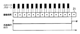
図4は、前述したX線平面検出器11の各画素21( 1列の画素 )とグリッド( GRID )パターン( 鉛部分で構成されたパターン )との位置関係及びX線を均等に曝射したときの各画素21の出力の状態を示す図である。
【0055】
なお、この図4は、説明を簡単にするため、グリッドパターンでは鉛部分を誇張( 実際の鉛部分と中間物質部分との太さの比とは異なる )し、画素は1列( 例えばデータ信号ラインに沿った画素の1列 )のみを最小の四角形の枠で示した。さらに、画素の各境界とグリッドパターンの各鉛部分の左端とを一致させた。
【0056】
前記X線平面検出器11の前記各画素21の中心間のピッチ( 以下画素ピッチと称する )をAmmとすると、前記グリッド12のグリッド周波数( 1mm当たりの鉛部分のペアライン数 )は、1/A又はN/A( Nは整数 )として設計される。すなわち、前記グリッド12の鉛部分のピッチは画素ピッチAと同じか又は画素ピッチAの整数( N )分の1として設計される。
【0057】
なお、ここではグリッド周波数を1/Aとして設計する。前記グリッド12の鉛部分のピッチはAとなる。例えばA=0.125mmとすると、グリッド周波数1/A=8LP/mm となる。
【0058】
このような構成の第1の実施の形態においては、X線を均等に曝射した時、各画素21からの出力を見ると、図4に示すように、どの画素21からの出力も、画素21のX線入射面( 前面 )に何も配置しない場合に比べて若干の出力低下があるが、モアレパターン( モアレ像 )等のうねりは見られない。画素21からの出力が低下するのは、X線の散乱線を遮断するグリッドの鉛部分は、検出すべきX線( 散乱線でない被検体を透過したX線 )をも遮断してしまうからである。
【0059】
この状況は画素とグリッドパターンとの位置関係をずらしても、グリッド周波数が1/Aであれば、どの鉛部分も1つの画素に対して同じ位置関係となり、出力低下の程度が変わるだけで、どの画素からの出力も同じ値になり、モアレパターン( モアレ像 )等のうねりは見られない。
【0060】
このようにこの第1の実施の形態によれば、X線平面検出器の画素ピッチAに対してグリッド周波数1/Aのグリッド12を使用することにより、グリッド12の各鉛部分が1つの画素に対して同じ位置関係になり、X線を均等に曝射した場合、各画素からの出力が同じ値となり、X線の散乱線の影響を除去できると共に、モアレ像の発生を防止して、良好・正確なX線画像を安定して得ることができる。
【0061】
なお、この第1の実施の形態では、グリッド周波数1/ALP/mm について説明したが、もちろん、グリッド周波数が1/ALP/mm の整数倍の、1画素に対して鉛部分が2本以上配置されるものでも良いものである。なおこの場合には、X線の散乱線の影響の除去の効果が高まるが、画素からの出力低下が増加することになる。
【0062】
この発明の第2の実施の形態を図5及び図6を参照して説明する。なお、この第2の実施の形態は、X線平面検出器に不感部分が存在するものにおいて、グリッドの鉛部分の配置について特定したものであるので、前述した第1の実施の形態で説明したX線撮像システムの構成は同じであるので、その説明は省略する( 図1及び図2参照 )。
【0063】
図5は、前記X線平面検出器11の一部の構成を模式的に示す図である。
このX線平面検出器11には、ライン方向( ゲート駆動ライン方向 )に不感部分( 光の検出ができない部分 )31が、最小の四角形の枠で示す画素( X線検出素子 )32の各列の間に設けられている。この不感部分31は、前記X線平面検出器11の構造上できるものである。黒丸は、画素のX線受感部の中心33を示し邸いる。この画素32間のピッチをBとする。
【0064】
図6は、前述したX線平面検出器11の各画素32( 1列の画素 )とグリッド( GRID )パターンとの位置関係及びX線を均等に曝射したときの各画素32の出力の状態を示す図である。
【0065】
なお、この図6は、説明を簡単にするため、グリッドパターンでは鉛部分を誇張( 実際の鉛部分と中間物質部分との太さの比とは異なる )し、画素は1列( 例えばデータ信号ラインに沿った画素の1列 )のみを最小の四角形の枠で示した。
【0066】
前記X線平面検出器11の前記各画素32の中心間のピッチ( 以下画素ピッチと称する )をBmmとすると、前記グリッド12のグリッド周波数は、1/B又はN/B( Nは整数 )として設計される。すなわち、前記グリッド12の鉛部分のピッチは画素ピッチBと同じか又は画素ピッチBの整数分の1として設計される。
【0067】
なお、ここではグリッド周波数を1/Bとして設計する。前記グリッド12の鉛部分のピッチはBとなる。さらに、このグリッド12は、その鉛部分がちょうど前記X線平面検出器11の前記不感部分31と一致するように配置して前記カセッテ1の前記きょう体15に固定される。
【0068】
このような構成の第2の実施の形態においては、X線を均等に曝射した時、各画素32からの出力を見ると、図6に示すように、どの画素32からの出力も出力低下もなく、モアレパターン( モアレ像 )等のうねりも見られない。
【0069】
このようにこの第2の実施の形態によれば、前述した第1の実施の形態と同様な効果を得ることができる。さらに、グリッド12の鉛部分をX線平面検出器11の不感部分31と一致するように配置してX線像カセッテ1のきょう体15に固定したことにより、画素32からの出力の低下がなく、X線画像を撮像することができる。
【0070】
なお、図6に示すものは、グリッドの鉛部分の幅が不感部分31の幅とほぼ同じ幅となっているが、鉛部分の幅は、必ずしも不感部分31の幅と同じである必要はなく、不感部分31の幅より狭くても、また広くても良いものである。ただし広い場合には、画素32の出力が低下するが、その低下を最小限に抑えることができる。
【0071】
もちろん、グリッド周波数を1/Bの整数倍にした場合にも、画素32のX線入射面に1本以上の鉛部分が配置されてしまうので、画素32からの出力が低下するが、それも最小限に抑えて、モアレパターン( モアレ像 )等のうねりを防止することができる。
【0072】
なお、上記実施の形態は、蛍光体、フォトダイオード、蓄積用コンデンサ、ΤFTによりX線を検出する場合について記載したが、蛍光体とフォトダイオードの代わりにX線を直接電気信号に変換する素子を用いる構成としても良い。
【0073】
【発明の効果】
以上詳述したようにこの発明によれば、X線平面検出器を使用して、グリッドによりX線の散乱線の影響を除去すると共にモアレ像の発生を防止することができるX線診断装置を提供できる。
【図面の簡単な説明】
【図1】この発明の第1の実施の形態のX線撮像システムの全体の構成を示すブロック図。
【図2】同実施の形態のX線撮像システムのX線平面検出器を収納したX線像検出カセッテを示す斜視図。
【図3】同実施の形態のX線撮像システムのX線平面検出器の一部の構成を模式的に示す図。
【図4】同実施の形態のX線撮像システムのX線平面検出器の各画素とグリッドパターンとの位置関係及びX線を均等に曝射したときの各画素の出力の状態を示す図。
【図5】この発明の第2の実施例のX線平面検出器の一部の構成を模式的に示す図。
【図6】同実施の形態のX線平面検出器の各画素とグリッドパターンとの位置関係及びX線を均等に曝射したときの各画素の出力の状態を示す図。
【図7】従来例のX線平面検出器を構成する実際のX線検出素子の要部構造を示す断面図。
【図8】同従来例のX線平面検出器を構成するX線検出素子を示す回路図。
【図9】同従来例のX線平面検出器の要部構成を示す回路図。
【図10】同従来例のX線平面検出器の各画素とグリッドパターンとの位置関係及びX線を均等に曝射したときの各画素の出力の状態を示す図。
【符号の説明】
1…X線像検出カセッテ、
4…データ保存媒体、
5…データリーダ、
6…画像再生機、
9…データベース、
11…X線平面検出器、
12…グリッド、
15…きょう体、
21,32…画素( X線検出素子 )、
31…不感部分。[0001]
BACKGROUND OF THE INVENTION
The present invention relates to an X-ray diagnostic apparatus using an X-ray flat panel detector that converts an X-ray image into an electrical signal.
[0002]
[Prior art]
An X-ray diagnostic apparatus exposes a subject to X-rays, detects X-rays transmitted through the subject with an X-ray detector, and captures an image of the transmitted X-rays.
Currently, what is used as an X-ray diagnostic apparatus is described below.
[0003]
1. Screen / film system
X-ray imaging is performed in a state in which an intensifying screen and an X-ray film are combined and held in a case called a cassette. In X-ray imaging, it is often used in combination with a bucky (grid that vibrates at high speed (GRID)) or the like for the purpose of removing the influence of scattered radiation. Since this cassette is relatively small and light, with a thickness of several millimeters, if the subject (patient) cannot move to the laboratory, bring it together with a mobile X-ray generator to the bedside. X-ray imaging may be performed.
[0004]
In addition, the cassette system found in an X-ray bed has a magazine for storing unphotographed film and photographed film, and a film transport unit. At the time of X-ray photography, the unphotographed film is preloaded with an X-ray grid or intensifying screen. It is conveyed to the predetermined | prescribed position arrange | positioned, and imaging is performed by an X-ray entering.
The imaged film can be observed as an X-ray image by performing development processing using an automatic developing device.
[0005]
The problems with the current screen / film system are as follows.
(1) Until the development is completed, care must be taken in handling the film so that the film is not exposed or damaged, and the operability is poor.
(2) Special processing equipment such as an automatic developer is required, and since these special processing equipment use water and chemicals, the installation location is limited, and these special processing equipment cannot be brought into the bedside.
[0006]
2. Computed radiography
This is an X-ray imaging method using a plate (imaging plate) coated with a stimulable phosphor instead of using a conventional film as an X-ray detector.
When X-rays are exposed to the imaging plate, the energy level of electrons is excited by the energy of the X-rays, and the X-ray intensity distribution is stored as a latent image. When a laser is later irradiated to excite electrons having a high energy level, the energy at that time is detected as light. Since this light is proportional to the energy of the X-rays absorbed by the imaging plate, the X-ray image can be accurately reproduced electrically.
[0007]
The problems with the current imaging plate include the following. (1) Poor resolution compared to the film system described above.
(2) There is a lot of noise.
(3) It is easy to get scratched and requires careful handling. If scratched, the performance deteriorates. (4) The reading device is expensive.
[0008]
3. I. I. (Image Intensifier)-TV System
This is a method of obtaining an X-ray image by combining an image intensifier that converts X-rays into light and a television set. In this method, the size of the X-ray input surface of the image intensifier is a size that can be imaged, and the size is approximately 16 inches.
[0009]
The X-ray image converted into light by the image intensifier is formed once at this output unit, and this output image is captured by a television camera via an optical system and output as an electrical image. .
This method has an advantage that an X-ray image can be observed in real time, but has a disadvantage that the resolution is lower than that of a film system and the apparatus of an imaging system becomes large.
[0010]
In recent years, the portability of the above-described screen / film system and imaging plate, the high resolution characteristics of the film / screen system, I. -An X-ray flat panel detector using TFT (thin film transistor) as a switching gate has attracted attention as an X-ray imaging system having the real-time property of a TV system.
[0011]
This X-ray flat panel detector is composed of a phosphor that converts X-rays into light, a photodiode that converts the light into electric charge, a capacitor that accumulates electric charge, and a TFT that reads out (outputs) electric charge, Photodiodes (and capacitors and TFTs) are two-dimensionally (planarly) arranged in an array.
[0012]
FIG. 7 is a diagram showing a configuration of an X-ray flat panel detector using a TFT-photodiode.
A
[0013]
Further, n + a ·
Thus, a TFT is formed in the TFT region.
[0014]
On the other hand, the
[0015]
A first polyimide resin layer 112 is formed on the TFT, and a transparent electrode 113 is formed on the photodiode. On the first polyimide resin layer 112, a
[0016]
A second
[0017]
The photodiode and the TFT are connected in a circuit as shown in FIG. The
[0018]
As will be described later, the gate terminal of the
In this way, one X-ray detection element is configured, and this X-ray detection element is two-dimensionally arranged to configure an X-ray flat panel detector.
[0019]
FIG. 9 is a circuit diagram showing a main configuration of the X-ray flat panel detector.
The X-ray flat panel detector has an
[0020]
Further, the gate terminal of the
[0021]
From each line output terminal of the
[0022]
The
[0023]
Therefore, when one line of
[0024]
This output signal is input to an A / D (analogue / digital)
When the reading of one line is completed in this way, reading of the next line is started.
[0025]
That is, the detection signal is read in order (one pixel at a time) for each
[0026]
In the X-ray flat panel detector having such a configuration, X-rays that have passed through the subject from above pass through the light reflecting layer 118 and enter the phosphor 117. At this time, visible light incident from above is reflected by the light reflecting layer 118 and is not incident on the phosphor 117.
[0027]
The incident X-ray energy is converted into light energy (visible light) by the phosphor 117, and the visible light passes through the transparent protective film 116 and the second
[0028]
This
[0029]
[Problems to be solved by the invention]
In portable cassettes such as conventional screen / film system films and imaging plates for computed radiography, a grid (GRID) that removes scattered radiation is a separate configuration when taking images on the bedside. Therefore, there is a problem that imaging is performed without a grid and scattered rays are included in the X-ray image.
[0030]
I. I. -In the TV system, when the grid was placed in front of the image intensifier, images were taken with the television camera depending on the relationship between the pixel pitch of the combined television camera (CCD camera, etc.) and the grid frequency. There has been a problem that a moire image as a kind of fixed pattern noise occurs in an image.
[0031]
As shown in FIG. 10, the moiré image causes the pitch of pixels to be picked up (for example, one column of pixels along the data signal line) (square frame, black circle indicates the center of the pixel) and moire generation. If the relationship between the period of the stripe pattern of the grid does not maintain a steady positional relationship between the pixel and the stripe pattern, as a result, a phenomenon of swaying amplitude fluctuation (moire phenomenon) with a long period occurs. Such a moire image should be removed from the image as noise.
[0032]
This is considered to occur similarly in the X-ray flat panel detector. That is, if the relationship between the pitch of the X-ray detection element and the period of the stripe pattern that blocks the X-rays of the grid does not maintain a steady positional relationship between the X-ray detection element and the stripe pattern, a moire image is generated. .
[0033]
Accordingly, an object of the present invention is to provide an X-ray diagnostic apparatus that uses an X-ray flat panel detector to remove the influence of X-ray scattered radiation by a grid and prevent the generation of a moire image. .
[0034]
[Means for Solving the Problems]
An X-ray diagnostic apparatus according to the present invention divides an X-ray tube that emits X-rays toward a subject and an X-ray image transmitted through the subject into pixels that are two-dimensionally arranged at a predetermined pitch. A planar detector for imaging, and a scattered radiation removal grid having a plate-like X-ray shielding member provided on the X-ray incident surface side of the planar detector so as to remove scattered X-rays incident on the planar detector; The planar detector and the scattered radiation removal grid are configured such that an X-ray insensitive portion on the X-ray image detection unit of the planar detector overlaps the X-ray blocking pattern of the scattered radiation removal grid. It is characterized by being.
[0041]
DETAILED DESCRIPTION OF THE INVENTION
A first embodiment of the present invention will be described with reference to FIGS.
FIG. 1 is a block diagram showing the overall configuration of an X-ray imaging system to which the present invention is applied.
[0042]
Reference numeral 1 denotes an X-ray image detection cassette using an X-ray flat panel detector. The X-ray exposure apparatus 2 generates X-rays and exposes a desired X-ray dose to a subject on a bed indicated by a broken line. X-rays transmitted through the subject 3 are detected by the X-ray image detection cassette 1.
[0043]
The X-ray image detection power set 1 includes an X-ray plane detector 11 for capturing an X-ray image, a
[0044]
Further, image data can be transferred by removing the data storage medium 4 from the X-ray image detection cassette 1 and attaching it to a
The
[0045]
The image player 6 is connected to a communication line (for example, LAN = local area network) 6, and the communication line 7 has an image player 6 and an
[0046]
For example, the image reproducing device 6 to which the
[0047]
In such a system, when the X-ray image detection cassette 1 and the X-ray exposure apparatus 2 are brought into the bed room and X-ray imaging is performed, the X-ray image obtained by the X-ray imaging is converted into the X-ray image detection cassette. Stored in the data storage medium 4 set to 1. The data storage medium 4 is removed from the X-ray image detection cassette 1 and set in the
[0048]
When a doctor makes a transfer request for an X-ray image of a desired patient from the
[0049]
Moreover, if the X-ray exposure apparatus 2, the X-ray, the
FIG. 2 is a perspective view of the X-ray image detection cassette 1.
[0050]
The
The
There are various grid frequencies indicating the intervals of the
[0051]
The X-ray flat panel detector 11 and peripheral circuits of the X-ray flat panel detector 11 are housed in a box formed by the
[0052]
FIG. 3 is a diagram schematically showing a partial configuration of the X-ray flat panel detector 11.
What is indicated by the smallest square frame is a
[0053]
The pitch A between the
A = 0.125mm
It becomes. This is a numerical value included in the pixel size of 0.05 to 0.3 mm of the currently developed X-ray flat panel detector.
[0054]
FIG. 4 shows the positional relationship between each pixel 21 (one row of pixels) of the X-ray flat panel detector 11 and the grid (GRID) pattern (pattern composed of a lead portion) and X-rays evenly exposed. It is a figure which shows the state of the output of each
[0055]
In FIG. 4, in order to simplify the description, the lead portion is exaggerated in the grid pattern (which is different from the thickness ratio between the actual lead portion and the intermediate material portion), and the pixels are arranged in one column (for example, a data signal). Only one column of pixels along the line) is indicated by the smallest square frame. Further, each pixel boundary and the left end of each lead portion of the grid pattern were matched.
[0056]
If the pitch between the centers of the
[0057]
Here, the grid frequency is designed to be 1 / A. The pitch of the lead portion of the
[0058]
In the first embodiment having such a configuration, when the output from each
[0059]
In this situation, even if the positional relationship between the pixel and the grid pattern is shifted, if the grid frequency is 1 / A, any lead portion has the same positional relationship with respect to one pixel, and the degree of output decrease is changed. The output from every pixel has the same value, and no swells such as moire patterns (moire images) are seen.
[0060]
As described above, according to the first embodiment, by using the
[0061]
In the first embodiment, the grid frequency 1 / ALP / mm has been described. Of course, two or more lead portions are arranged for one pixel whose grid frequency is an integer multiple of 1 / ALP / mm. What is done is good. In this case, the effect of removing the influence of the scattered X-rays is enhanced, but the output from the pixel is increased.
[0062]
A second embodiment of the present invention will be described with reference to FIGS. In addition, since this 2nd Embodiment specified the arrangement | positioning of the lead part of a grid in what a dead part exists in an X-ray flat panel detector, it demonstrated in 1st Embodiment mentioned above. Since the configuration of the X-ray imaging system is the same, the description thereof is omitted (see FIGS. 1 and 2).
[0063]
FIG. 5 is a diagram schematically showing a partial configuration of the X-ray flat panel detector 11.
In this X-ray flat panel detector 11, insensitive portions (portions where light cannot be detected) 31 in the line direction (gate drive line direction) are arranged in each column of pixels (X-ray detecting elements) 32 indicated by the smallest rectangular frame. It is provided between. This
[0064]
FIG. 6 shows the positional relationship between each pixel 32 (one row of pixels) and the grid (GRID) pattern of the X-ray flat panel detector 11 and the output state of each
[0065]
In FIG. 6, for the sake of simplicity, the lead portion is exaggerated in the grid pattern (which differs from the actual thickness ratio between the lead portion and the intermediate portion), and the pixels are arranged in one column (for example, a data signal). Only one column of pixels along the line) is indicated by the smallest square frame.
[0066]
If the pitch between the centers of the
[0067]
Here, the grid frequency is designed to be 1 / B. The pitch of the lead portion of the
[0068]
In the second embodiment having such a configuration, when the output from each
[0069]
As described above, according to the second embodiment, the same effect as that of the first embodiment described above can be obtained. Furthermore, since the lead portion of the
[0070]
6, the width of the lead portion of the grid is substantially the same as the width of the
[0071]
Of course, even when the grid frequency is set to an integral multiple of 1 / B, one or more lead portions are disposed on the X-ray incident surface of the
[0072]
Although the above embodiment has described the case where X-rays are detected by a phosphor, a photodiode, a storage capacitor, and a ΤFT, an element that directly converts X-rays into an electrical signal is used instead of the phosphor and the photodiode. It is good also as a structure to use.
[0073]
【The invention's effect】
As described above in detail, according to the present invention, there is provided an X-ray diagnostic apparatus that uses an X-ray flat panel detector to remove the influence of scattered X-rays by a grid and prevent the generation of moire images. Can be provided.
[Brief description of the drawings]
FIG. 1 is a block diagram showing the overall configuration of an X-ray imaging system according to a first embodiment of the present invention.
FIG. 2 is a perspective view showing an X-ray image detection cassette containing an X-ray flat panel detector of the X-ray imaging system of the embodiment.
FIG. 3 is a diagram schematically showing a configuration of a part of an X-ray flat panel detector of the X-ray imaging system of the embodiment.
FIG. 4 is a diagram showing the positional relationship between each pixel of the X-ray flat panel detector and the grid pattern of the X-ray imaging system of the embodiment and the output state of each pixel when X-rays are evenly exposed.
FIG. 5 is a diagram schematically showing a partial configuration of an X-ray flat panel detector according to a second embodiment of the present invention.
6 is a diagram showing a positional relationship between each pixel and the grid pattern of the X-ray flat panel detector according to the embodiment and an output state of each pixel when X-rays are evenly exposed. FIG.
FIG. 7 is a cross-sectional view showing a main structure of an actual X-ray detection element constituting an X-ray flat panel detector of a conventional example.
FIG. 8 is a circuit diagram showing an X-ray detection element constituting the X-ray flat panel detector of the conventional example.
FIG. 9 is a circuit diagram showing a main configuration of the conventional X-ray flat panel detector.
FIG. 10 is a diagram showing a positional relationship between each pixel and a grid pattern of the X-ray flat panel detector of the conventional example and an output state of each pixel when X-rays are evenly exposed.
[Explanation of symbols]
1 ... X-ray image detection cassette,
4. Data storage medium,
5 ... Data reader,
6 ... Image player,
9 ... Database,
11 ... X-ray flat panel detector,
12 ... Grid,
15 ... The body,
21, 32... Pixel (X-ray detection element),
31 ... Insensitive part.
Claims (4)
前記被検体を透過したX線像を所定ピッチで2次元的に配列された画素に分けて撮像する平面検出器と、
前記平面検出器に入射する散乱X線を除去するように前記平面検出器のX線入射面側に設けられた板状のX線遮蔽部材を有する散乱線除去グリッドとを備え、
前記平面検出器と前記散乱線除去グリッドとは、前記平面検出器のX線像検出部上のX線不感部分が前記散乱線除去グリッドのX線遮断パターンに重なるように構成されていることを特徴とするX線診断装置。An X-ray tube that emits X-rays toward the subject;
A flat panel detector that captures an X-ray image transmitted through the subject by dividing it into two-dimensionally arranged pixels at a predetermined pitch;
A scattered radiation removal grid having a plate-like X-ray shielding member provided on the X-ray incident surface side of the planar detector so as to remove scattered X-rays incident on the planar detector;
The planar detector and the scattered radiation removal grid are configured such that an X-ray insensitive portion on the X-ray image detection unit of the planar detector overlaps with the X-ray blocking pattern of the scattered radiation removal grid. A characteristic X-ray diagnostic apparatus.
Priority Applications (2)
| Application Number | Priority Date | Filing Date | Title |
|---|---|---|---|
| JP23832295A JP3776485B2 (en) | 1995-09-18 | 1995-09-18 | X-ray diagnostic equipment |
| US08/715,086 US5666395A (en) | 1995-09-18 | 1996-09-17 | X-ray diagnostic apparatus |
Applications Claiming Priority (1)
| Application Number | Priority Date | Filing Date | Title |
|---|---|---|---|
| JP23832295A JP3776485B2 (en) | 1995-09-18 | 1995-09-18 | X-ray diagnostic equipment |
Publications (2)
| Publication Number | Publication Date |
|---|---|
| JPH0975332A JPH0975332A (en) | 1997-03-25 |
| JP3776485B2 true JP3776485B2 (en) | 2006-05-17 |
Family
ID=17028495
Family Applications (1)
| Application Number | Title | Priority Date | Filing Date |
|---|---|---|---|
| JP23832295A Expired - Fee Related JP3776485B2 (en) | 1995-09-18 | 1995-09-18 | X-ray diagnostic equipment |
Country Status (2)
| Country | Link |
|---|---|
| US (1) | US5666395A (en) |
| JP (1) | JP3776485B2 (en) |
Families Citing this family (43)
| Publication number | Priority date | Publication date | Assignee | Title |
|---|---|---|---|---|
| JPH0998970A (en) * | 1995-10-06 | 1997-04-15 | Canon Inc | X-ray photographing equipment |
| JPH10305030A (en) * | 1997-03-06 | 1998-11-17 | Canon Inc | Radiographic device and driving method for the same |
| JP2000512084A (en) * | 1997-04-02 | 2000-09-12 | コーニンクレッカ フィリップス エレクトロニクス エヌ ヴィ | X-ray apparatus having a sensor matrix |
| WO1998044568A2 (en) * | 1997-04-02 | 1998-10-08 | Koninklijke Philips Electronics N.V. | X-ray apparatus with sensor matrix |
| US5847398A (en) * | 1997-07-17 | 1998-12-08 | Imarad Imaging Systems Ltd. | Gamma-ray imaging with sub-pixel resolution |
| US6304626B1 (en) * | 1998-10-20 | 2001-10-16 | Kabushiki Kaisha Toshiba | Two-dimensional array type of X-ray detector and computerized tomography apparatus |
| US6366643B1 (en) | 1998-10-29 | 2002-04-02 | Direct Radiography Corp. | Anti scatter radiation grid for a detector having discreet sensing elements |
| CA2346652A1 (en) * | 1998-10-29 | 2000-05-11 | Direct Radiography Corp. | Anti scatter radiation grid for a detector having discreet sensing elements |
| US6690767B2 (en) | 1998-10-29 | 2004-02-10 | Direct Radiography Corp. | Prototile motif for anti-scatter grids |
| US6181773B1 (en) | 1999-03-08 | 2001-01-30 | Direct Radiography Corp. | Single-stroke radiation anti-scatter device for x-ray exposure window |
| US6373062B1 (en) * | 1999-06-30 | 2002-04-16 | Siemens Medical Solutions Usa, Inc. | Interdigital photodetector for indirect x-ray detection in a radiography imaging system |
| US6900442B2 (en) | 1999-07-26 | 2005-05-31 | Edge Medical Devices Ltd. | Hybrid detector for X-ray imaging |
| CA2345303A1 (en) | 1999-07-26 | 2001-02-01 | Albert Zur | Digital detector for x-ray imaging |
| JP2001189929A (en) * | 1999-12-28 | 2001-07-10 | Shimadzu Corp | X-ray fluoroscopic imaging system |
| US6826256B2 (en) | 2000-02-04 | 2004-11-30 | Canon Kabushiki Kaisha | Apparatus and method for a radiation image through a grid |
| US20010033638A1 (en) * | 2000-02-04 | 2001-10-25 | Hitoshi Inoue | Image acquisition method and apparatus |
| JP4505949B2 (en) * | 2000-06-06 | 2010-07-21 | 株式会社島津製作所 | Radiation imaging equipment |
| JP3987676B2 (en) | 2000-07-10 | 2007-10-10 | 株式会社日立メディコ | X-ray measuring device |
| JP2002151669A (en) * | 2000-11-14 | 2002-05-24 | Toshiba Corp | X-ray imaging device |
| US20020090055A1 (en) * | 2000-11-27 | 2002-07-11 | Edge Medical Devices Ltd. | Digital X-ray bucky including grid storage |
| US6795528B2 (en) * | 2001-01-12 | 2004-09-21 | Canon Kabushiki Kaisha | Radiographic apparatus, radiographic method, and computer-readable storage medium |
| US7142705B2 (en) | 2001-05-01 | 2006-11-28 | Canon Kabushiki Kaisha | Radiation image processing apparatus, image processing system, radiation image processing method, storage medium, and program |
| JP4118535B2 (en) * | 2001-07-03 | 2008-07-16 | 株式会社日立メディコ | X-ray inspection equipment |
| JP3848107B2 (en) * | 2001-07-24 | 2006-11-22 | キヤノン株式会社 | Radiation imaging equipment |
| DE10211948A1 (en) * | 2002-03-18 | 2003-10-09 | Siemens Ag | X-ray computer tomography detector |
| JP3793139B2 (en) * | 2002-10-25 | 2006-07-05 | キヤノン株式会社 | X-ray imaging device |
| US7196332B2 (en) * | 2004-05-04 | 2007-03-27 | General Electric Company | Monolithic x-ray detector with staggered detection areas |
| JP2008510960A (en) * | 2004-08-20 | 2008-04-10 | コーニンクレッカ フィリップス エレクトロニクス エヌ ヴィ | Microelectronic system with protective layer |
| JP3928647B2 (en) * | 2004-09-24 | 2007-06-13 | 株式会社日立製作所 | Radiation imaging apparatus and nuclear medicine diagnostic apparatus using the same |
| CN101868836B (en) * | 2007-11-19 | 2013-09-18 | 皇家飞利浦电子股份有限公司 | A radiation detector comprising an imaging radiation-collimating structure |
| JP5112097B2 (en) * | 2008-02-04 | 2013-01-09 | 株式会社東芝 | Breast X-ray diagnostic device |
| JP5193636B2 (en) * | 2008-03-17 | 2013-05-08 | 富士フイルム株式会社 | Radiation imaging equipment |
| US8873703B2 (en) * | 2008-05-08 | 2014-10-28 | Arineta Ltd. | X ray imaging system with scatter radiation correction and method of using same |
| FR2939019B1 (en) * | 2008-11-28 | 2011-07-15 | Gen Electric | MEDICAL IMAGING METHOD IN WHICH IMAGES ARE ACQUIRED THROUGH AN ANTI-DIFFUSING GRID |
| US20120082294A1 (en) * | 2010-10-02 | 2012-04-05 | Varian Medical Systems, Inc. | X-ray system and method |
| US9968316B2 (en) | 2010-12-29 | 2018-05-15 | General Electric Company | High-frequency anti-scatter grid movement profile for line cancellation |
| US8956045B2 (en) * | 2011-09-30 | 2015-02-17 | Fujifilm Corporation | Radiation imaging apparatus |
| JP5749148B2 (en) * | 2011-12-21 | 2015-07-15 | ジーイー・メディカル・システムズ・グローバル・テクノロジー・カンパニー・エルエルシー | Radiation tomography apparatus, radiation detection apparatus, and spatial resolution switching method in radiation tomography |
| US9230702B2 (en) * | 2012-08-17 | 2016-01-05 | General Electric Company | System and method for reducing grid line image artifacts |
| DE102017200653A1 (en) * | 2017-01-17 | 2018-07-19 | Siemens Healthcare Gmbh | X-ray detector with an arrangement of a pixelated second electrode and a scattered radiation grid |
| NL2021258B1 (en) * | 2018-06-14 | 2019-12-20 | Illumina Inc | Device for luminescent imaging |
| US10960232B2 (en) * | 2018-07-28 | 2021-03-30 | Varian Medical Systems, Inc. | Single-pass imaging and radiation treatment delivery via an extended rotation gantry |
| JP6593853B1 (en) * | 2018-09-19 | 2019-10-23 | 株式会社三田屋製作所 | X-ray detector with grid and grid |
Family Cites Families (7)
| Publication number | Priority date | Publication date | Assignee | Title |
|---|---|---|---|---|
| US4689487A (en) * | 1984-09-03 | 1987-08-25 | Kabushiki Kaisha Toshiba | Radiographic image detection apparatus |
| US4672207A (en) * | 1985-08-21 | 1987-06-09 | The United States Of America As Represented By The United States Department Of Energy | Readout system for multi-crystal gamma cameras |
| US4785186A (en) * | 1986-10-21 | 1988-11-15 | Xerox Corporation | Amorphous silicon ionizing particle detectors |
| US5179284A (en) * | 1991-08-21 | 1993-01-12 | General Electric Company | Solid state radiation imager having a reflective and protective coating |
| US5596198A (en) * | 1994-04-22 | 1997-01-21 | The Regents, University Of California | Gamma ray camera |
| US5436958A (en) * | 1994-08-03 | 1995-07-25 | General Electric Company | Adjustable collimator |
| US5557650A (en) * | 1995-03-10 | 1996-09-17 | General Electric Company | Method for fabricating an anti-scatter X-ray grid device for medical diagnostic radiography |
-
1995
- 1995-09-18 JP JP23832295A patent/JP3776485B2/en not_active Expired - Fee Related
-
1996
- 1996-09-17 US US08/715,086 patent/US5666395A/en not_active Expired - Lifetime
Also Published As
| Publication number | Publication date |
|---|---|
| JPH0975332A (en) | 1997-03-25 |
| US5666395A (en) | 1997-09-09 |
Similar Documents
| Publication | Publication Date | Title |
|---|---|---|
| JP3776485B2 (en) | X-ray diagnostic equipment | |
| JP3494683B2 (en) | Radiation detection system, cassette for radiation detector, and radiation image capturing method. | |
| US6528796B1 (en) | Radiation image pickup device and radiation image pickup system | |
| JP3647440B2 (en) | X-ray equipment | |
| US7564037B2 (en) | Image sensor, image-sensing apparatus using the image sensor, and image-sensing system | |
| JP2002505752A (en) | Optical quantum imaging device without film | |
| EP2080038A2 (en) | Retrofit digital mammography detector | |
| JP2006280576A (en) | Radiographic equipment | |
| US20130193339A1 (en) | Radiation irradiation initiation determination apparatus, radiation image capturing device, radiation image capture control apparatus, radiation irradiation initiation determination method, and computer readable medium | |
| CN104244829A (en) | Radiology detector device and radiography system | |
| CN104379061A (en) | Radiology detector device and radiography system | |
| JP2002200064A (en) | Imaging device, imaging system, imaging method, and recording medium | |
| JPS62167535A (en) | Radiation image pick-up apparatus | |
| JPH11271454A (en) | Radiation image pickup device and system | |
| KR20000060730A (en) | Method of and Apparatus for high resolution X ray photographing using multiple imaging devices. | |
| JP2004154409A (en) | Picture imaging unit for breast | |
| JP3989659B2 (en) | Radiation detection cassette | |
| JP3715873B2 (en) | Imaging apparatus, radiation imaging apparatus, and radiation imaging system using the same | |
| JPH11188021A (en) | X ray face sensor and radiographic device | |
| JP3560624B2 (en) | Image signal reading method and apparatus | |
| JP2013011553A (en) | Radiographic system, radiographic apparatus and radiographic method | |
| JP2005124868A (en) | X-ray imaging apparatus | |
| JP2006506157A (en) | X-ray inspection equipment | |
| JP4724277B2 (en) | Image photographing apparatus and image photographing method | |
| JP2018021828A (en) | Radiation imaging apparatus and radiation imaging system |
Legal Events
| Date | Code | Title | Description |
|---|---|---|---|
| A131 | Notification of reasons for refusal |
Free format text: JAPANESE INTERMEDIATE CODE: A131 Effective date: 20050426 |
|
| A521 | Request for written amendment filed |
Free format text: JAPANESE INTERMEDIATE CODE: A523 Effective date: 20050624 |
|
| TRDD | Decision of grant or rejection written | ||
| A01 | Written decision to grant a patent or to grant a registration (utility model) |
Free format text: JAPANESE INTERMEDIATE CODE: A01 Effective date: 20060221 |
|
| A61 | First payment of annual fees (during grant procedure) |
Free format text: JAPANESE INTERMEDIATE CODE: A61 Effective date: 20060223 |
|
| R150 | Certificate of patent or registration of utility model |
Free format text: JAPANESE INTERMEDIATE CODE: R150 |
|
| FPAY | Renewal fee payment (event date is renewal date of database) |
Free format text: PAYMENT UNTIL: 20100303 Year of fee payment: 4 |
|
| FPAY | Renewal fee payment (event date is renewal date of database) |
Free format text: PAYMENT UNTIL: 20100303 Year of fee payment: 4 |
|
| FPAY | Renewal fee payment (event date is renewal date of database) |
Free format text: PAYMENT UNTIL: 20110303 Year of fee payment: 5 |
|
| LAPS | Cancellation because of no payment of annual fees |