JP3775259B2 - Nitride semiconductor laser device - Google Patents
Nitride semiconductor laser device Download PDFInfo
- Publication number
- JP3775259B2 JP3775259B2 JP2001233486A JP2001233486A JP3775259B2 JP 3775259 B2 JP3775259 B2 JP 3775259B2 JP 2001233486 A JP2001233486 A JP 2001233486A JP 2001233486 A JP2001233486 A JP 2001233486A JP 3775259 B2 JP3775259 B2 JP 3775259B2
- Authority
- JP
- Japan
- Prior art keywords
- layer
- type
- nitride semiconductor
- active layer
- laser element
- Prior art date
- Legal status (The legal status is an assumption and is not a legal conclusion. Google has not performed a legal analysis and makes no representation as to the accuracy of the status listed.)
- Expired - Lifetime
Links
Images


Description
【0001】
【発明の属する技術分野】
本発明は窒化物半導体(InXAlYGa1−X−YN、0≦X、0≦Y、X+Y≦1)よりなるレーザ素子に関する。
【0002】
【従来の技術】
活性層にSiがドープされたレーザ素子が、特開平7−297494号公報に記載されている。この公報にはGaNよりなる膜厚の厚い活性層にSiをドープして閾値電流を低下させることが開示されている。
【0003】
しかし、前記公報のように、単一層の膜厚が例えば0.1μm以上もある厚膜の活性層を有する素子構造では出力が弱く、レーザ発振させるのは非常に困難である。また活性層を単一膜厚が100オングストーム近辺にある井戸層と障壁層とを積層した多重量子井戸構造の活性層を有するレーザ素子が、例えば特開平8−64909号公報に記載されている。この公報には、井戸層にZnがドープされた多重量子井戸構造の活性層を有するレーザ素子が記載されており、井戸層に極微量のZnをドープすることにより、価電子帯近くにアクセプター的な不純物準位を形成して、閾値電流を低下させることが示されている。さらにまた、特開平6−268257号公報にはInXGa1−XNよりなる井戸層と、InYGa1−YNよりなる障壁層とを積層した多重量子井戸構造の活性層を有する発光素子が示されており、さらにこの公報には活性層にn型不純物、またはp型不純物をドープしても良いことが記載されている。
【0004】
このように活性層にn型、p型不純物をドープして、バンドギャップ内に不純物準位を形成することにより、発光素子の発光出力を高めたり、レーザ素子の閾値電流を低下させることが知られている。
【0005】
【発明が解決しようとする課題】
ところで、本出願人は最近窒化物半導体により、パルス電流において、室温での410nmのレーザ発振を発表した(例えば、Jpn.J.Appl.Phys. Vol35 (1996) pp.L74-76)。発表したレーザ素子はいわゆる電極ストライプ型のレーザ素子であり、ノンドープInGaNが積層された多重量子井戸構造の活性層を有するものである。
【0006】
しかしながら、前記窒化物半導体レーザは未だパルス発振でしかなく、しかも閾値電流は1〜2Aもある。窒化物半導体で連続発振させるためには、閾値電流をさらに低下させる必要がある。
【0007】
従って、本発明の目的とするところは、窒化物半導体よりなるレーザ素子の発光出力を高め、さらに閾値電流を小さくして、室温での連続発振を目指すことにある。
【0008】
インジウムを含む窒化物半導体よりなる井戸層と、井戸層よりもバンドギャップが大きい窒化物半導体よりなる障壁層とが積層されてなる多重量子井戸構造の活性層を有する窒化物半導体レーザ素子において、前記活性層は、In X Ga 1−X N(0< X ≦1)よりなる井戸層と、In X ' Ga 1−X ' N(0< X ’≦1、 X' < X )よりなる障壁層が積層され、前記活性層の1つの井戸層においてIn組成の多い領域とIn組成の少ない領域とを有し、かつ、前記障壁層中にn型不純物がドープされていることを特徴とする窒化物半導体レーザ素子。
【0009】
前記n型不純物は、Siであることを特徴とする請求項1に記載の窒化物半導体レーザ素子。
【0010】
前記障壁層中のSi濃度は、1×10 18 /cm 3 〜1×10 22 /cm 3 であることを特徴とする請求項1又は2に記載の窒化物半導体レーザ素子。
【0011】
前記活性層に接して、Alを含むp型の窒化物半導体層を有することを請求項1乃至3のいずれか一項に記載の窒化物半導体レーザ素子。
【0012】
請求項1乃至4に記載の窒化物半導体レーザ素子において、n電極と接するn型コンタクト層は、AlとGaを含むn型の窒化物半導体を有することを特徴とする窒化物半導体レーザ素子。
【0020】
【発明の実施の形態】
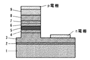
図1は本発明の一実施例に係るレーザ素子の構造を示す模式的な断面図である。基本的な構造としては、基板1の上に、バッファ層2、n型コンタクト層3、n型クラッド層4、不純物がドープされた多重量子井戸構造を有する活性層5、第1のp型層6、第2のp型層7、第3のp型層8、p型コンタクト層9が順に積層された電極ストライプ型の構造を有しており、n型コンタクト層にはストライプ状の負電極、p型コンタクト層には正電極が設けられている。
【0021】
このレーザ素子を各パルス電流を流した際のスペクトルを図3に示す。図3において(a)は280mA(閾値直後)、(b)は295mA、(c)は320mA、(d)は340mAでの発光スペクトルを示している。(b)、(c)、(d)は発振時のスペクトルを示している。
【0022】
(a)は発振直後のスペクトルを示し、この状態ではおよそ404.2nm付近にある主発光ピークの前後に小さな発光ピークが多数(ファブリペローモード)出現してレーザ発振直後の状態であることが分かる。これがいわゆる縦モードのスペクトルである。電流値を上げると(b)に示すように、そのスペクトルがシングルモードとなって404.2nm付近のレーザ発振を示す。次からが本発明の特徴であり、さらに電流を増加させると、(c)に示すように、403.3nm(3.075eV)、403.6nm(3.072eV)、403.9nm(3.070eV)、404.2nm(3.068eV)、404.4nm(3.066eV)というように、主発光ピークの他に、強度の大きな発光ピークが1meV〜100meVの間隔で不規則に出現する。さらに(d)では前記ピークの他に、また新たなピークがはっきりと出現しており。これらのスペクトル間隔は一定ではなく明らかに縦モードのスペクトルと異なる。
【0023】
一般に、半導体レーザの場合、レーザ発振すると、レーザ光の縦モードによる小さな発光ピークが主発光ピークの前後に多数出現する。この場合の発光スペクトルは、ほぼ等間隔の発光ピークよりなっている。赤色半導体レーザでは、その発光ピークの間隔はおよそ0.2nmである。青色半導体レーザではおよそ0.05nm(1meV)以下である(但し、青色半導体レーザの縦モードは共振器長が600μmにおいて、本出願人により初めて計測された。)。つまり、図3(a)、(b)の状態では通常のレーザ素子の挙動を示している。しかし、本発明のレーザ素子の場合、(c)、(d)に示すように、明らかに従来のレーザ素子の縦モードによる発光ピークとは異なった等間隔でないピークが多数出現している。これは図3の電流値による各スペクトルを比較しても分かる。本発明のレーザ素子では、このような発光スペクトルが出現することにより、出力が高くなる。
【0024】
なぜ、このようなピークが発生するとレーザ素子の出力が高くなるのかは定かではないが、例えば次のようなことが考えられる。活性層が量子井戸構造の場合、井戸層の膜厚は100オングストローム以下、好ましくは70オングストローム以下、最も好ましくは50オングストローム以下に調整される。一方、障壁層も150オングストローム以下、好ましくは100オングストローム以下に調整される。本発明の発光素子では、このような単一膜厚が数十オングストロームの薄膜を積層した場合、井戸層、障壁層共、均一な膜厚で成長しておらず、凹凸のある層が幾重にも重なり合った状態となっている。図2は図1のレーザ素子において活性層5とクラッド層との界面の状態を拡大して示す模式的な断面図である。図2に示すように、このような凹凸のある活性層を、活性層よりもバンドギャップの大きいクラッド層で挟むダブルヘテロ構造を実現すると、活性層に注入された電子とホールとが、凹部にも閉じ込められるようになって、クラッド層の縦方向と共に縦横の両方向に閉じ込められる。このため、キャリアが約10〜70オングストローム凹凸差がある3次元のInGaNよりなる量子箱、あるいは量子ディスクに閉じ込められたようになって、従来の量子井戸構造とは違った、量子効果が出現する。従って、多数の量子準位に基づく発光が室温でも観測されるようになり、発光スペクトルの1meV〜100meVの間隔で多数の発光ピークが観測される。また、他の理由としては、三次元のInGaNよりなる小さな量子箱にキャリアが閉じ込められるので、エキシトン効果が顕著に現れてきて多数の発光ピークが観測される。
【0025】
また、このようにInGaN井戸層に多数の凹凸が発生する理由の一つとして、In組成の面内不均一が考えられる。即ち、単一井戸層内において、In組成の大きい領域と、少ない領域とができるために、井戸層表面に多数の凹凸が発生するのである。InGaNは混晶を成長させにくい材料であり、InNとGaNとが相分離する傾向にある。このためIn組成の不均一な領域ができる。そして、このIn組成の高い領域に電子と正孔とが局在して、エキシトン発光、あるいはバイエキシトン発光して、レーザの出力が向上し、多数のピークができる。特にレーザ素子ではこのバイエキシトンレーザ発振することにより、量子ディスク、量子箱と同等になって多数のピークが出現し、この多数のピークによりレーザ素子の閾値が下がり、出力が向上する。なおエキシトンとは電子と正孔とが弱いクーロン力でくっついてペアになったものである。
【0026】
さらに、活性層中にn型不純物及び/又はp型不純物をドープすることにより、閾値電流を低下させることができる。これらの不純物をドープすることにより、活性層のIn組成の多い領域に局在化しているエキシトンが、今度はそれよりもさらに深い不純物の準位に局在化するようになって、エキシトン発光の効果が顕著となることにより、閾値の低下が起きる。
【0027】
本発明のレーザ素子の活性層について述べたことを、図6のエネルギーバンド図でわかりやすく示す。図6Aは多重量子井戸構造の活性層のエネルギーバンドを示しており、図6Bは、図6Aの単一井戸層のエネルギーバンドを拡大して示すものである。前記したように、井戸層においてIn組成の面内不均一があるということは、Bに示すように単一のInGaN井戸層幅にバンドギャップの異なるInGaN領域が存在する。従って、伝導帯にある電子は一度、In組成の大きいInGaN領域に落ちて、そこから価電子帯にある正孔と再結合することによりhνのエネルギーを放出する。このことは、電子と正孔とが井戸層幅のIn組成の多い領域に局在化して、局在エキシトンを形成し、レーザの閾値の低下を助ける。閾値が下がり、出力が高くなるのはこの局在エキシトンの効果によるものである。さらに、この井戸層にSi等のn型不純物、Zn等のp型不純物をドープすることにより、伝導帯と価電子帯との間にさらに不純物レベルの準位ができる。図6BではSiと、Znとでもってその準位を示している。不純物をドープすると不純物レベルのエネルギー準位が形成される。そのため電子はより深い準位へ落ち、正孔はp型不純物のレベルに移動して、そこで電子と正孔とが再結合して、hν'のより小さいエネルギーを放出する。このことは電子と正孔とがさらに局在化することを意味し、この局在したエキシトン効果によりレーザの閾値が下がるのである。多数のピークが出現するのは、この局在エキシトンに加えて、三次元的に閉じ込められた量子箱の効果により多数の量子準位間の発光が出てくるからである。
【0028】
n型不純物には、例えばSi、Ge、Sn、Se、Sを挙げることができる。p型不純物には、例えばZn、Cd、Mg、Be、Ca等を挙げることができる。これらの不純物を活性層中、特に好ましくは井戸層中にドープすることにより、量子準位間に、不純物レベルの発光を起こさせ、バンド間のエネルギー準位を小さくして、閾値を低下させることができる。なお、n型不純物、p型不純物両方をドープしてもよいことは言うまでもない。
【0029】
特に好ましくはn型不純物、中でもSi、Geをドープすることにより、発光強度を強めると共に、閾値電流を低下させることができる。図4は井戸層にドープしたSi濃度と、閾値電流の低下率の割合を示す図である。具体的には平均膜厚30オングストロームのInGaNよりなる井戸層と、平均膜厚70オングストローム障壁とを5層積層した多重量子井戸構造の活性層を有するレーザ素子において、前記井戸層中にSiをドープした際のレーザ素子の閾値の低下の割合を示しており、図に示す各点は実際のSi濃度を示している。この図に示すようにSiをドープすることにより、閾値電流を最大で50%近く低下させることができる。従って、好ましいSi濃度は、1×10¹⁸/cm3〜1×1022/cm3の範囲にあり、さらに好ましくは5×1018/cm3〜2×1021/cm3、最も好ましくは1×1019/cm3〜1×1021/cm3である。なおこの図はSiについて示したものであるが、他のn型不純物、Ge、Sn等に対しても同様の傾向があることを確認した。
【0030】
図5は井戸層にドープしたMg濃度と、閾値電流の低下率の割合を示す図である。これも同じく平均膜厚30オングストロームのInGaNよりなる井戸層と、平均膜厚70オングストローム障壁とを5層積層した多重量子井戸構造の活性層を有するレーザ素子において、前記井戸層中にMgをドープした際のレーザ素子の閾値の低下の割合を示しており、図に示す各点は実際のMg濃度を示している。この図に示すように、Mgをドープすることにより、閾値電流を25%近く低下させることができる。好ましいMg濃度は、1×10¹⁷/cm3〜1×1022/cm3の範囲にあり、さらに好ましくは1×1018/cm3〜2×1021/cm3、最も好ましくは1×1018/cm3〜1×1021/cm3である。なお、この図はMgについて示したものであるが、他のp型不純物、Zn、Cd、Be等に対しても同様の傾向があることを確認した。
【0031】
【実施例】
以下、MOVPE法を用いて、図1に示す構造のレーザ素子を得る方法を説明する。図1は本発明のレーザ素子の一構造を示すものであって、本発明のレーザ素子はこの構造に限定されるものではない。なお本発明において示すInXGa1−XN、AlYGa1−YN等の一般式は、単に窒化物半導体の組成式を示しているに過ぎず、異なる層が同一の式で示されていても、それらの層が同一の組成を示すものでは決してない。
【0032】
[実施例1]
サファイアのA面を主面とする基板1を用意し、この基板1をMOVPE装置の反応容器内に設置した後、原料ガスにTMG(トリメチルガリウム)と、アンモニアを用い、温度500℃でサファイア基板1の表面にGaNよりなるバッファ層2を200オングストロームの膜厚で成長させる。基板1にはA面の他にC面、R面等の面方位を有するサファイアが使用でき、サファイアの他、スピネル111面(MgAl2O4)、SiC、MgO、Si、ZnO、GaN等の単結晶よりなる、公知の基板が用いられる。バッファ層2は基板と窒化物半導体との格子不整合を緩和するために設けられ、通常、GaN、AlN、AlGaN等が1000オングストローム以下の膜厚で成長されるが、窒化物半導体と格子定数の近い基板、格子整合した基板を用いる場合、成長方法、成長条件等の要因によっては成長されないこともあるので、省略することもできる。但し、サファイア、スピネルのように、窒化物半導体と格子定数が異なる基板を用いる場合、特開平4−297023号公報に記載されるように、200℃以上、900℃以下の温度でバッファ層2を成長させると、次に高温で成長させる窒化物半導体層の結晶性が飛躍的に良くなる。
【0033】
続いて温度を1050℃に上げ、原料ガスにTMG、TMA(トリメチルアルミニウム)、アンモニア、ドナー不純物としてSiH4(シラン)ガスを用いて、SiドープAl0.3Ga0.7Nよりなるn型コンタクト層3を4μmの膜厚で成長させる。
【0034】
n型コンタクト層3は光閉じ込め層としても作用する。n型コンタクト層3をAlとGaとを含むn型窒化物半導体、好ましくはn型AlYGa1-YN(0<Y<1)とすることにより、活性層との屈折率差が大きくでき、光閉じ込め層としてのクラッド層、及び電流を注入するコンタクト層として作用する。さらに、このコンタクト層をAlYGa1−YNとすることにより、活性層の発光をn型コンタクト層内で広がりにくくできるので、閾値が低下する。n型コンタクト層3をAlYGa1−YNとする場合、基板側のAl混晶比が小さく、活性層側のAl混晶比が大きい構造、即ち組成傾斜構造とすることが望ましい。前記構造とすることにより、結晶性の良いn型コンタクト層が得られるので、結晶性の良いn型コンタクト層の上に積層する窒化物半導体の結晶性も良くなるため、素子全体の結晶性が良くなり、ひいては閾値の低下、素子の信頼性が格段に向上する。また活性層側のAl混晶比が大きいために、活性層との屈折率差も大きくなり光閉じ込め層として有効に作用する。また、このn型コンタクト層3をGaNとしてもよい。GaNの場合、n電極とのオーミック特性については非常に優れている。コンタクト層をGaNとすると、GaNコンタクト層と、活性層との間にAlGaNよりなる光閉じ込め層を設ける必要がある。このn型コンタクト層3の膜厚は0.1μm以上、5μm以下に調整することが望ましい。0.1μm以下であると、光閉じ込め層として作用しにくく、また、電極を同一面側に設ける場合に、精密なエッチングレートの制御をせねばならないので不利である。一方、5μmよりも厚いと、結晶中にクラックが入りやすくなる傾向にある。
【0035】
続いて、温度を1050℃に保持し、原料ガスにTMG、アンモニア、シランガスを用いて、Siドープn型GaNよりなるn型クラッド層4を500オングストロームの膜厚で成長させる。
【0036】
このn型クラッド層4はn層側の光ガイド層、および活性層にInGaNを成長させる際のバッファ層として作用し、n型GaNの他、n型InGaNを成長させることもできる。バッファ層と成長させる場合には0.05μm以下の膜厚で成長させることが望ましい。また、前記のようにコンタクト層2をGaNで成長させた場合、このn型クラッド層4は、光閉じ込め層として作用させるためにAlGaNで成長させる必要がある。AlGaN層の場合、膜厚は0.01μm〜0.5μmの膜厚で成長させることが望ましい。0.01μmより薄いと光閉じ込め層として作用しにくく、0.5μmよりも厚いと結晶中にクラックが入りやすい傾向にある。
【0037】
次に、温度を750℃にして、原料ガスにTMG、TMI(トリメチルインジウム)、アンモニア、不純物ガスとしてシランガスを用いてSiをドープした活性層5を成長させる。活性層5は、まずSiを1×10²⁰/cm3の濃度でドープしたIn0.2Ga0.8Nよりなる井戸層を25オングストロームの膜厚で成長させる。次にシランガスを止めて、TMIのモル比を変化させるのみで同一温度で、ノンドープIn0.01Ga0.95Nよりなる障壁層を50オングストロームの膜厚で成長させる。この操作を13回繰り返し、最後に井戸層を成長させ総膜厚0.1μmの多重量子井戸構造よりなる活性層5を成長させる。
【0038】
活性層5は、少なくとも井戸層がInを含む窒化物半導体を含む多重量子井戸構造とする。多重量子井戸構造とは、井戸層と障壁層とを積層したものであり、本発明の場合、井戸層がInを含む窒化物半導体で構成されていれば、障壁層は井戸層よりもバンドギャップが大きければ特にInを含む必要はない。好ましくは、InXGa1−XN(0<X≦1)よりなる井戸層と、InX’Ga1−X’N(0≦X'<1、X'<X)よりなる障壁層とを積層した構造とする。三元混晶のInGaNは四元混晶のものに比べて結晶性が良い物が得られるので、発光出力が向上する。また障壁層は井戸層よりもバンドギャップエネルギーを大きくして、井戸+障壁+井戸+・・・+障壁+井戸層(その逆でもよい。)となるように積層して多重量子井戸構造を構成する。井戸層の膜厚は70オングストローム以下、さらに望ましくは50オングストローム以下に調整することが好ましい。また障壁層の厚さも150オングストローム以下、さらに望ましくは100オングストローム以下の厚さに調整することが望ましい。井戸層が70オングストロームよりも厚いか、または障壁層が150オングストロームよりも厚いと、レーザ素子の出力が低下する傾向にある。このように活性層をInGaNを積層したMQWとすると、量子準位間発光で約365nm〜660nm間での高出力なLDを実現することができる。特に好ましい態様として、両方の層をInGaNとすると、InGaNは、GaN、AlGaN結晶に比べて結晶が柔らかい。そのため第1のp型層であるAlGaNの厚さを厚くできるのでレーザ発振が実現できる。またn型不純物は本実施例のように井戸層にドープしてもよいし、また障壁層にドープしてもよく、さらに井戸層、障壁層両方にドープしてもよい。
【0039】
活性層5の膜厚は、n型コンタクト層3をAlYGa1−YNとした場合、200オングストローム以上、さらに好ましくは300オングストローム以上の膜厚で成長させることが望ましい。なぜなら、MQWよりなる活性層を厚く成長させることにより、活性層の最外層近辺が光ガイド層として作用する。つまり、n型コンタクト層3と第3のp型層8とが光閉じ込め層として作用し、活性層の最外層近傍が光ガイド層として作用する。活性層の膜厚の上限は特に限定するものではないが、通常は0.5μm以下に調整することが望ましい。
【0040】
次に、原料ガスにTMG、TMA、アンモニア、p型不純物としてCp2Mg(シクロペンタジエニルマグネシウム)を用いて、Mgドープp型Al0.2Ga0.8Nよりなる第1のp型層6を100オングストロームの膜厚で成長させる。
【0041】
第1のp型層6はAlを含むp型の窒化物半導体で構成し、好ましくは三元混晶若しくは二元混晶のAlYGa1−YN(0<Y≦1)を成長させることが望ましい。さらに、このAlGaNは後に述べる第3のp型層8よりも膜厚を薄く形成することが望ましく、好ましくは10オングストローム以上、0.5μm以下に調整する。この第1のp型層6を活性層5に接して形成することにより、素子の出力が格段に向上する。これは、第1のp型層6成長時に、活性層のInGaNが分解するのを抑える作用があるためと推察されるが、詳しいことは不明である。第1のp型層6は好ましく10オングストローム〜0.5μm以下の膜厚で成長させることが望ましいが、省略することもできる。
【0042】
次に、温度を1050℃にし、TMG、アンモニア、Cp2Mgを用いて、Mgドープp型GaNよりなる第2のp型層7を500オングストロームの膜厚で成長させる。
【0043】
この第2のp型層7はp層側の光ガイド層若しくはバッファ層として作用し、好ましくは二元混晶または三元混晶のInYGa1−YN(0≦Y<1)を成長させる。第2のp型層7は、活性層の膜厚が薄い場合に成長させると光ガイド層として作用する。また第1のp型層6がAlGaN等よりなるので、この層がバッファ層のような作用をして、次に成長させる第3のp型層8をクラック無く結晶性良く成長できる。つまり、AlGaNの上に直接バンドギャップが大きいAlGaNを積層すると、後から成長させたバンドギャップが大きいAlGaNにクラックが入りやすくなるので、この第2のp型層7を介することによりクラックを入りにくくしている。第2のp型層7は、通常100オングストローム〜0.5μm程度の膜厚で成長させることが望ましいが、省略することもできる。
【0044】
次に、温度を1050℃に上げ、原料ガスにTMG、TMA、アンモニア、アクセプター不純物としてCp2Mgを用いて、MgドープAl0.3Ga0.7Nよりなる第3のp型層8を0.3μmの膜厚で成長させる。
【0045】
第3のp型層8は、Alを含む窒化物半導体で構成し、好ましくは二元混晶または三元混晶のAlYGa1−YN(0<Y≦1)を成長させる。第3のp型層8は、光閉じ込め層として作用し、0.1μm〜1μmの膜厚で成長させることが望ましく、AlGaNのようなAlを含むp型窒化物半導体とすることにより、好ましく光閉じ込め層として作用する。この第3のp型層も活性層5をInを含む窒化物半導体としているために、成長可能となる。つまり、InGaNを含む活性層が緩衝層のような作用をするために、AlGaNを厚膜で成長させやすくなる。逆にAlを含む窒化物半導体層の上に、直接光閉じ込め層となるような厚膜で、Alを含む窒化物半導体を成長させることは難しい傾向にある。
【0046】
続いて、1050℃でTMG、アンモニア、Cp2Mgを用い、Mgドープp型GaNよりなるp型コンタクト層9を0.5μmの膜厚で成長させる。
【0047】
p型コンタクト層9は電流を注入する層であり、p型の窒化物半導体(InXAlYGa1−X−YN、0≦X、0≦Y、X+Y≦1)で構成することができ、特にInGaN、GaN、その中でもMgをドープしたp型GaNとすると、最もキャリア濃度の高いp型層が得られて、正電極と良好なオーミック接触が得られ、しきい値電流を低下させることができる。正電極の材料としてはNi、Pd、Ir、Rh、Pt、Ag、Au等の比較的仕事関数の高い金属又は合金がオーミックが得られやすい。
【0048】
以上のようにして窒化物半導体を積層したウェーハを反応容器から取り出し、図1に示すように最上層のp型コンタクト層9より選択エッチングを行い、n型コンタクト層3の表面を露出させ、露出したn型コンタクト層3と、p型コンタクト層9との表面にそれぞれストライプ状の電極を形成した後、サファイア基板のR面からウェーハを劈開して、バー状にし、さらにストライプ状の電極に直交する方向にレーザの共振面を形成し、共振器長は600μmとする。後は、常法に従い、共振面に誘電体多層膜よりなる反射鏡を形成した後、ストライプ状の電極に平行な位置でウェーハを分割してレーザチップとする。このレーザチップをヒートシンクに設置し、順方向電流320mAのパルス発振を試みたところ、図3(c)に示すような不規則な位置に発光ピークを有するレーザ発振を示し、活性層に不純物をドープしていないレーザ素子に比較して、閾値電流は50%低下し、出力は30%向上した。
【0049】
[実施例2]
実施例1の活性層を成長させる工程において、不純物ガスとしてシランガスの代わりにジエチルジンクを用いて、Znを1×10¹⁹/cm3の濃度でドープしたIn0.2Ga0.8Nよりなる井戸層を25オングストローム、ノンドープIn0.01Ga0.95Nよりなる障壁層を50オングストロームの膜厚で成長させて、同じく総膜厚0.1μmの多重量子井戸構造よりなる活性層5を成長させる他は、同様にして、共振器長600μmのレーザ素子を得たところ、活性層に不純物をドープしていないレーザ素子に比較して、閾値電流は25%低下し、出力は10%向上した。
【0050】
[実施例3]
実施例1の活性層を成長させる工程において、不純物ガスとしてシランガス、およびジエチルジンクを用いて、Siを1×10²⁰/cm3、及びZnを1×1019/cm3の濃度でドープしたIn0.2Ga0.8Nよりなる井戸層を25オングストローム、ノンドープIn0.01Ga0.95Nよりなる障壁層を50オングストロームの膜厚で成長させて、同じく総膜厚0.1μmの多重量子井戸構造よりなる活性層5を成長させる他は、同様にして、共振器長600μmのレーザ素子を得たところ、活性層に不純物をドープしていないレーザ素子に比較して、閾値電流は60%低下し、出力は35%向上した。
【0051】
【発明の効果】
以上説明したように、本発明のレーザ素子は、活性層の1つの井戸層においてIn組成の多い領域とIn組成の少ない領域とを有することにより発光出力が向上する。さらに、活性層中にn型不純物、p型不純物がドープされていることにより、発光出力を低下させることなく閾値を低下させることができる。このため、発光出力が高く閾値の低いレーザ素子を実現することができる。また、本発明のレーザ素子を埋め込みへテロ型、屈折率導波型、実効屈折率導波型等の横モードの安定化を図るレーザ素子とすることにより、さらに閾値電流が下がる可能性がある。
【図面の簡単な説明】
【図1】 本発明の一実施例に係るレーザ素子の構造を示す模式断面図。
【図2】 図1のレーザ素子の活性層付近を拡大して示す模式断面図。
【図3】 本発明のレーザ素子にパルス電流を流した際の発光スペクトルを各電流値で比較して示す図。
【図4】 活性層にドープしたSi濃度と、レーザ素子の閾値電流の低下率との関係を示す図。
【図5】 活性層にドープしたMg濃度と、レーザ素子の閾値電流の低下率との関係を示す図。
【図6】 本発明のレーザ素子の井戸層のエネルギーバンド図。
【符号の説明】
1・・・基板
2・・・バッファ層
3・・・n型コンタクト層
4・・・n型クラッド層
5・・・活性層
6・・・第1のp型層
7・・・第2のp型層
8・・・第3のp型層
9・・・p型コンタクト層[0001]
BACKGROUND OF THE INVENTION
The present invention relates to a nitride semiconductor (InXAlYGa1-XYN, 0 ≦ X, 0 ≦ Y, X + Y ≦ 1).
[0002]
[Prior art]
A laser element in which an active layer is doped with Si is described in JP-A-7-297494. This publication discloses that the threshold current is reduced by doping Si into a thick active layer made of GaN.
[0003]
However, as described in the above publication, an element structure having a thick active layer with a single layer thickness of, for example, 0.1 μm or more has a weak output and is very difficult to cause laser oscillation. A laser element having an active layer having a multiple quantum well structure in which a well layer and a barrier layer having a single film thickness in the vicinity of 100 angstroms are stacked is described, for example, in JP-A-8-64909. . This publication describes a laser element having an active layer having a multiple quantum well structure in which a well layer is doped with Zn. By doping a very small amount of Zn into a well layer, an acceptor-like structure is obtained. It has been shown that a simple impurity level is formed to reduce the threshold current. Furthermore, JP-A-6-268257 discloses In.XGa1-XN well layer and InYGa1-YA light-emitting element having an active layer having a multiple quantum well structure in which a barrier layer made of N is stacked is shown. Further, this publication may be doped with an n-type impurity or a p-type impurity. Are listed.
[0004]
It is known that doping the n-type and p-type impurities in the active layer and forming impurity levels in the band gap increases the light emission output of the light emitting element and lowers the threshold current of the laser element. It has been.
[0005]
[Problems to be solved by the invention]
By the way, the present applicant recently announced a 410 nm laser oscillation at a room temperature with a nitride semiconductor at a pulse current (for example, Jpn.J.Appl.Phys.Vol35 (1996) pp.L74-76). The announced laser device is a so-called electrode stripe type laser device, and has an active layer of a multiple quantum well structure in which non-doped InGaN is stacked.
[0006]
However, the nitride semiconductor laser is still only pulsed and has a threshold current of 1 to 2A. In order to continuously oscillate the nitride semiconductor, it is necessary to further reduce the threshold current.
[0007]
Accordingly, an object of the present invention is to increase the light emission output of a laser element made of a nitride semiconductor and further reduce the threshold current to achieve continuous oscillation at room temperature.
[0008]
In a nitride semiconductor laser device having an active layer having a multiple quantum well structure in which a well layer made of a nitride semiconductor containing indium and a barrier layer made of a nitride semiconductor having a larger band gap than the well layer are stacked.The active layer is made of In. X Ga 1-X N (0 < X ≦ 1) well layer and In X ' Ga 1-X ' N (0 < X '≦ 1, X ' < X ) Barrier layer is laminated,The well layer of the active layer has a region with a large In composition and a region with a small In composition, andN-type impurity is doped in the barrier layerA nitride semiconductor laser device characterized by the above.
[0009]
The nitride semiconductor laser element according to claim 1, wherein the n-type impurity is Si.
[0010]
The Si concentration in the barrier layer is 1 × 10 18 / Cm 3 ~ 1x10 22 / Cm 3 The nitride semiconductor laser element according to
[0011]
4. The nitride semiconductor laser element according to claim 1, further comprising a p-type nitride semiconductor layer containing Al in contact with the active layer. 5.
[0012]
5. The nitride semiconductor laser device according to claim 1, wherein the n-type contact layer in contact with the n-electrode includes an n-type nitride semiconductor containing Al and Ga. 6.
[0020]
DETAILED DESCRIPTION OF THE INVENTION
FIG. 1 is a schematic cross-sectional view showing the structure of a laser device according to an embodiment of the present invention. As a basic structure, a
[0021]
The spectrum when each pulse current is passed through this laser element is shown in FIG. In FIG. 3, (a) shows an emission spectrum at 280 mA (immediately after the threshold), (b) shows 295 mA, (c) shows 320 mA, and (d) shows an emission spectrum at 340 mA. (B), (c), and (d) show spectra during oscillation.
[0022]
(A) shows the spectrum immediately after oscillation, and in this state, it can be seen that many small emission peaks (Fabry-Perot mode) appear before and after the main emission peak in the vicinity of about 404.2 nm, and that the state is immediately after laser oscillation. . This is the so-called longitudinal mode spectrum. When the current value is increased, as shown in (b), the spectrum becomes a single mode, and laser oscillation near 404.2 nm is exhibited. The following is a feature of the present invention. When the current is further increased, as shown in (c), 403.3 nm (3.075 eV), 403.6 nm (3.072 eV), 403.9 nm (3.070 eV). ), 404.2 nm (3.068 eV), and 404.4 nm (3.066 eV), in addition to the main emission peak, emission peaks with high intensity appear irregularly at intervals of 1 meV to 100 meV. Further, in (d), a new peak clearly appears in addition to the peak. These spectral intervals are not constant and are clearly different from the longitudinal mode spectra.
[0023]
In general, in the case of a semiconductor laser, when laser oscillation occurs, many small emission peaks due to the longitudinal mode of laser light appear before and after the main emission peak. The emission spectrum in this case consists of emission peaks at approximately equal intervals. In the red semiconductor laser, the interval between the emission peaks is about 0.2 nm. For a blue semiconductor laser, it is about 0.05 nm (1 meV) or less (however, the longitudinal mode of the blue semiconductor laser was measured for the first time by the present applicant at a resonator length of 600 μm). That is, the behavior of a normal laser element is shown in the states of FIGS. However, in the case of the laser element of the present invention, as shown in (c) and (d), there are clearly many peaks that are not equally spaced apart from the emission peak due to the longitudinal mode of the conventional laser element. This can also be seen by comparing the spectra according to the current values in FIG. In the laser device of the present invention, the output is increased by the appearance of such an emission spectrum.
[0024]
The reason why the output of the laser element increases when such a peak occurs is not clear, but the following may be considered, for example. When the active layer has a quantum well structure, the thickness of the well layer is adjusted to 100 angstroms or less, preferably 70 angstroms or less, and most preferably 50 angstroms or less. On the other hand, the barrier layer is also adjusted to 150 angstroms or less, preferably 100 angstroms or less. In the light emitting device of the present invention, when such a thin film having a single film thickness of several tens of angstroms is stacked, neither the well layer nor the barrier layer grows with a uniform film thickness, and the uneven layer is overlapped. Are also in an overlapping state. FIG. 2 is a schematic cross-sectional view showing an enlarged state of the interface between the
[0025]
In addition, in-plane non-uniformity of the In composition can be considered as one of the reasons for the large number of irregularities in the InGaN well layer. That is, since a region with a large In composition and a region with a small In composition can be formed in a single well layer, many irregularities are generated on the surface of the well layer. InGaN is a material in which a mixed crystal is difficult to grow, and InN and GaN tend to phase-separate. For this reason, a region having a non-uniform In composition is formed. Then, electrons and holes are localized in the region having a high In composition, and exciton light emission or biexiton light emission is performed, so that the output of the laser is improved and a large number of peaks are formed. In particular, in a laser element, this bi-exciton laser oscillation causes a large number of peaks to appear in the same manner as the quantum disk and quantum box, and the threshold value of the laser element decreases due to the large number of peaks, and the output is improved. Exciton is a pair in which electrons and holes are bonded together by a weak Coulomb force.
[0026]
Furthermore, the threshold current can be reduced by doping the active layer with n-type impurities and / or p-type impurities. By doping these impurities, the exciton localized in the region with a large In composition in the active layer is now localized in a deeper impurity level, and the exciton emission When the effect becomes significant, the threshold value decreases.
[0027]
What has been described about the active layer of the laser element of the present invention is shown in an easily understandable manner in the energy band diagram of FIG. 6A shows an energy band of an active layer having a multiple quantum well structure, and FIG. 6B shows an enlarged energy band of the single well layer of FIG. 6A. As described above, in-plane nonuniformity of the In composition in the well layer means that there are InGaN regions having different band gaps in a single InGaN well layer width as shown in FIG. Accordingly, electrons in the conduction band once fall into an InGaN region having a large In composition, and recombine with holes in the valence band, thereby releasing hν energy. This localizes electrons and holes in the well layer-wide region with a large In composition, forms localized excitons, and helps to lower the laser threshold. The lower threshold and higher output are due to the effect of this localized exciton. Further, by doping this well layer with an n-type impurity such as Si or a p-type impurity such as Zn, a level of an impurity level can be further formed between the conduction band and the valence band. In FIG. 6B, the level is shown by Si and Zn. When an impurity is doped, an energy level at an impurity level is formed. Therefore, the electrons fall to a deeper level, and the holes move to the level of the p-type impurity, where the electrons and holes recombine and release a smaller energy of hν ′. This means that electrons and holes are further localized, and this localized exciton effect lowers the laser threshold. The reason why a large number of peaks appear is that, in addition to the localized excitons, light is emitted between a large number of quantum levels due to the effect of the quantum box confined in three dimensions.
[0028]
Examples of the n-type impurity include Si, Ge, Sn, Se, and S. Examples of the p-type impurity include Zn, Cd, Mg, Be, and Ca. By doping these impurities into the active layer, particularly preferably into the well layer, light emission at the impurity level is caused between the quantum levels, the energy level between the bands is reduced, and the threshold is lowered. Can do. Needless to say, both n-type and p-type impurities may be doped.
[0029]
Particularly preferably, doping the n-type impurity, particularly Si or Ge, can increase the emission intensity and reduce the threshold current. FIG. 4 is a diagram showing the ratio of Si concentration doped into the well layer and the rate of decrease in threshold current. Specifically, in a laser element having an active layer having a multiple quantum well structure in which a well layer made of InGaN having an average film thickness of 30 angstroms and an average film thickness of 70 angstrom barriers are stacked, the well layer is doped with Si. The ratio of the decrease in the threshold value of the laser element at this time is shown, and each point shown in the figure shows the actual Si concentration. As shown in this figure, by doping Si, the threshold current can be reduced by nearly 50% at maximum. Therefore, the preferred Si concentration is 1 × 10¹⁸/cm3~ 1x10²²/cm3And more preferably 5 × 10¹⁸/cm3~ 2x10²¹/cm3, Most preferably 1 × 10¹⁹/cm3~ 1x10²¹/cm3It is. Although this figure is shown for Si, it was confirmed that the same tendency was observed for other n-type impurities, Ge, Sn, and the like.
[0030]
FIG. 5 is a graph showing the Mg concentration doped in the well layer and the ratio of the reduction rate of the threshold current. This is also a laser element having an active layer having a multiple quantum well structure in which a well layer made of InGaN having an average film thickness of 30 angstroms and an average film thickness of 70 angstrom barriers are laminated, and the well layer is doped with Mg. The ratio of the decrease in the threshold value of the laser element is shown, and each point shown in the figure indicates the actual Mg concentration. As shown in this figure, the threshold current can be reduced by nearly 25% by doping Mg. The preferred Mg concentration is 1 × 10¹⁷/cm3~ 1x10²²/cm3And more preferably 1 × 10¹⁸/cm3~ 2x10²¹/cm3, Most preferably 1 × 10¹⁸/cm3~ 1x10²¹/cm3It is. In addition, although this figure showed about Mg, it confirmed that there existed the same tendency also about other p-type impurities, Zn, Cd, Be, etc.
[0031]
【Example】
Hereinafter, a method of obtaining the laser element having the structure shown in FIG. 1 using the MOVPE method will be described. FIG. 1 shows one structure of the laser element of the present invention, and the laser element of the present invention is not limited to this structure. In the present invention, InXGa1-XN, AlYGa1-YGeneral formulas such as N merely indicate the composition formula of the nitride semiconductor, and even if different layers are indicated by the same formula, these layers never show the same composition.
[0032]
[Example 1]
A substrate 1 having a sapphire A surface as a main surface is prepared, and this substrate 1 is placed in a reaction vessel of a MOVPE apparatus, and then TMG (trimethylgallium) and ammonia are used as source gases at a temperature of 500 ° C. A
[0033]
Subsequently, the temperature is raised to 1050 ° C., TMG, TMA (trimethylaluminum), ammonia, and SiH as donor impurities are used as source gases.4Using (silane) gas, the n-type contact layer 3 made of Si-doped Al0.3Ga0.7N is grown to a thickness of 4 μm.
[0034]
The n-type contact layer 3 also functions as an optical confinement layer. By making the n-type contact layer 3 an n-type nitride semiconductor containing Al and Ga, preferably n-type AlYGa1-YN (0 <Y <1), the refractive index difference from the active layer can be increased, and optical confinement can be achieved. It acts as a cladding layer as a layer and a contact layer for injecting current. Further, this contact layer is made of Al.YGa1-YBy setting N, the light emission of the active layer can be made difficult to spread in the n-type contact layer, so that the threshold value is lowered. The n-type contact layer 3 is made of AlYGa1-YIn the case of N, it is desirable to have a structure in which the Al mixed crystal ratio on the substrate side is small and the Al mixed crystal ratio on the active layer side is large, that is, a composition gradient structure. With this structure, an n-type contact layer with good crystallinity can be obtained, so that the crystallinity of the nitride semiconductor stacked on the n-type contact layer with good crystallinity is also improved. As a result, the threshold value is lowered and the reliability of the element is remarkably improved. In addition, since the Al mixed crystal ratio on the active layer side is large, the refractive index difference from the active layer is also large, which effectively acts as a light confinement layer. The n-type contact layer 3 may be GaN. In the case of GaN, the ohmic characteristics with the n electrode are very excellent. When the contact layer is GaN, it is necessary to provide an optical confinement layer made of AlGaN between the GaN contact layer and the active layer. The film thickness of the n-type contact layer 3 is desirably adjusted to 0.1 μm or more and 5 μm or less. When the thickness is 0.1 μm or less, it is difficult to act as a light confinement layer, and when the electrodes are provided on the same surface side, a precise etching rate must be controlled, which is disadvantageous. On the other hand, if it is thicker than 5 μm, cracks tend to be easily formed in the crystal.
[0035]
Subsequently, the temperature is maintained at 1050 ° C., and the n-
[0036]
The n-type clad
[0037]
Next, the temperature is set to 750 ° C., and the
[0038]
The
[0039]
The thickness of the
[0040]
Next, TMG, TMA, ammonia, and Cp2Mg (cyclopentadienylmagnesium) as the p-type impurity are used as source gases, and the first p-
[0041]
The first p-
[0042]
Next, the temperature is set to 1050 ° C., and the second p-type layer 7 made of Mg-doped p-type GaN is grown to a thickness of 500 Å using TMG, ammonia, and
[0043]
The second p-type layer 7 functions as a light guide layer or a buffer layer on the p-layer side, and preferably a binary mixed crystal or a ternary mixed crystal InYGa1-YN (0 ≦ Y <1) is grown. The second p-type layer 7 acts as a light guide layer when grown when the active layer is thin. Further, since the first p-
[0044]
Next, the temperature is raised to 1050 ° C., TMG, TMA, ammonia,
[0045]
The third p-
[0046]
Subsequently, a p-type contact layer 9 made of Mg-doped p-type GaN is grown to a thickness of 0.5 μm using TMG, ammonia, and
[0047]
The p-type contact layer 9 is a layer for injecting current, and a p-type nitride semiconductor (InXAlYGa1-XYN, 0.ltoreq.X, 0.ltoreq.Y, X + Y.ltoreq.1). In particular, when p-type GaN doped with InGaN, GaN, and Mg is used, a p-type layer with the highest carrier concentration is obtained. Good ohmic contact with the positive electrode can be obtained, and the threshold current can be reduced. As the material of the positive electrode, a metal or alloy having a relatively high work function such as Ni, Pd, Ir, Rh, Pt, Ag, Au, or the like tends to provide an ohmic property.
[0048]
The nitride semiconductor laminated wafer as described above is taken out of the reaction vessel and selectively etched from the uppermost p-type contact layer 9 as shown in FIG. 1 to expose the surface of the n-type contact layer 3 and expose it. After forming striped electrodes on the surfaces of the n-type contact layer 3 and the p-type contact layer 9, the wafer is cleaved from the R surface of the sapphire substrate to form a bar and orthogonal to the striped electrode. The resonant surface of the laser is formed in the direction of the laser, and the resonator length is 600 μm. Thereafter, in accordance with an ordinary method, a reflecting mirror made of a dielectric multilayer film is formed on the resonance surface, and then the wafer is divided at a position parallel to the striped electrode to form a laser chip. When this laser chip was placed on a heat sink and pulse oscillation with a forward current of 320 mA was attempted, laser oscillation with emission peaks at irregular positions as shown in FIG. 3C was exhibited, and the active layer was doped with impurities. The threshold current was reduced by 50% and the output was improved by 30% compared to a laser element that was not.
[0049]
[Example 2]
In the step of growing the active layer of Example 1, using Zn as the impurity gas instead of silane gas, Zn was 1 × 10¹⁹/cm3A well layer made of In0.2Ga0.8N doped at a concentration of 25 angstroms and a barrier layer made of non-doped In0.01Ga0.95N are grown to a thickness of 50 angstroms. A laser element having a resonator length of 600 μm was obtained in the same manner except that the
[0050]
[Example 3]
In the step of growing the active layer of Example 1, Si was used in an amount of 1 × 10 6 by using silane gas and diethyl zinc as impurity gases.20/cm3, And Zn 1 × 10¹⁹/cm3A well layer made of In0.2Ga0.8N doped at a concentration of 25 angstroms and a barrier layer made of non-doped In0.01Ga0.95N are grown to a thickness of 50 angstroms. A laser element having a cavity length of 600 μm was obtained in the same manner except that the
[0051]
【The invention's effect】
As described above, the laser device of the present invention has a light emission output improved by having a region with a large In composition and a region with a small In composition in one well layer of the active layer. Further, since the n-type impurity and the p-type impurity are doped in the active layer, the threshold value can be reduced without reducing the light emission output. For this reason, a laser element having a high light emission output and a low threshold value can be realized. In addition, the threshold current may be further reduced by using the laser element of the present invention as a laser element that stabilizes a transverse mode such as a buried hetero type, refractive index guided type, or effective refractive index guided type. .
[Brief description of the drawings]
FIG. 1 is a schematic cross-sectional view showing the structure of a laser device according to an embodiment of the present invention.
2 is an enlarged schematic cross-sectional view showing the vicinity of an active layer of the laser device of FIG.
FIG. 3 is a diagram showing emission spectra when a pulse current is passed through the laser element of the present invention by comparing each current value.
FIG. 4 is a graph showing the relationship between the Si concentration doped in the active layer and the threshold current reduction rate of the laser element.
FIG. 5 is a graph showing the relationship between the Mg concentration doped in the active layer and the reduction rate of the threshold current of the laser element.
FIG. 6 is an energy band diagram of a well layer of the laser device of the present invention.
[Explanation of symbols]
1 ... Board
2 ... Buffer layer
3 ... n-type contact layer
4 ... n-type cladding layer
5 ... Active layer
6: First p-type layer
7: Second p-type layer
8: Third p-type layer
9 ... p-type contact layer
Claims (5)
前記活性層は、In X Ga 1−X N(0< X ≦1)よりなる井戸層と、In X ' Ga 1−X ' N(0< X ’≦1、 X' < X )よりなる障壁層が積層され、
前記活性層の1つの井戸層においてIn組成の多い領域とIn組成の少ない領域とを有し、
かつ、前記障壁層中にn型不純物がドープされていることを特徴とする窒化物半導体レーザ素子。In a nitride semiconductor laser device having an active layer having a multiple quantum well structure in which a well layer made of a nitride semiconductor containing indium and a barrier layer made of a nitride semiconductor having a larger band gap than the well layer are stacked.
The active layer, In X Ga 1-X N (0 <X ≦ 1) and a well layer made of, In X 'Ga 1-X ' N (0 <X '≦ 1, X'<X) from become barriers Layers are stacked,
One well layer of the active layer has a region with a large In composition and a region with a small In composition,
A nitride semiconductor laser element, wherein the barrier layer is doped with an n-type impurity .
Priority Applications (1)
| Application Number | Priority Date | Filing Date | Title |
|---|---|---|---|
| JP2001233486A JP3775259B2 (en) | 2001-08-01 | 2001-08-01 | Nitride semiconductor laser device |
Applications Claiming Priority (1)
| Application Number | Priority Date | Filing Date | Title |
|---|---|---|---|
| JP2001233486A JP3775259B2 (en) | 2001-08-01 | 2001-08-01 | Nitride semiconductor laser device |
Related Parent Applications (1)
| Application Number | Title | Priority Date | Filing Date |
|---|---|---|---|
| JP15781296A Division JPH1012969A (en) | 1996-06-19 | 1996-06-19 | Nitride semiconductor laser element |
Publications (3)
| Publication Number | Publication Date |
|---|---|
| JP2002151797A JP2002151797A (en) | 2002-05-24 |
| JP2002151797A5 JP2002151797A5 (en) | 2004-07-15 |
| JP3775259B2 true JP3775259B2 (en) | 2006-05-17 |
Family
ID=19065255
Family Applications (1)
| Application Number | Title | Priority Date | Filing Date |
|---|---|---|---|
| JP2001233486A Expired - Lifetime JP3775259B2 (en) | 2001-08-01 | 2001-08-01 | Nitride semiconductor laser device |
Country Status (1)
| Country | Link |
|---|---|
| JP (1) | JP3775259B2 (en) |
Families Citing this family (1)
| Publication number | Priority date | Publication date | Assignee | Title |
|---|---|---|---|---|
| JP2009054616A (en) * | 2007-08-23 | 2009-03-12 | Sharp Corp | Method for manufacturing nitride semiconductor light-emitting element, and the nitride semiconductor light-emitting layer |
-
2001
- 2001-08-01 JP JP2001233486A patent/JP3775259B2/en not_active Expired - Lifetime
Also Published As
| Publication number | Publication date |
|---|---|
| JP2002151797A (en) | 2002-05-24 |
Similar Documents
| Publication | Publication Date | Title |
|---|---|---|
| JP3374737B2 (en) | Nitride semiconductor device | |
| JP4075324B2 (en) | Nitride semiconductor device | |
| KR100902109B1 (en) | Gallium nitride compound semiconductor element | |
| JP4441563B2 (en) | Nitride semiconductor laser device | |
| WO2002005399A1 (en) | Nitride semiconductor device | |
| JPH1012969A (en) | Nitride semiconductor laser element | |
| JP3660446B2 (en) | Nitride semiconductor device and manufacturing method thereof | |
| JP2004104157A (en) | Nitride semiconductor device | |
| JP3424465B2 (en) | Nitride semiconductor device and method of growing nitride semiconductor | |
| JP2003204122A (en) | Nitride semiconductor element | |
| JP4291960B2 (en) | Nitride semiconductor device | |
| JP3651260B2 (en) | Nitride semiconductor device | |
| JPH1065213A (en) | Nitride semiconductor element | |
| KR100625835B1 (en) | Nitride Semiconductor Device | |
| JP3282175B2 (en) | Nitride semiconductor device | |
| JP3951973B2 (en) | Nitride semiconductor device | |
| JP3366188B2 (en) | Nitride semiconductor device | |
| JP3434162B2 (en) | Nitride semiconductor device | |
| JP4360066B2 (en) | Gallium nitride light emitting device | |
| JP3496480B2 (en) | Nitride semiconductor device | |
| JP3775259B2 (en) | Nitride semiconductor laser device | |
| JP3772651B2 (en) | Nitride semiconductor laser device | |
| JP3218595B2 (en) | Nitride semiconductor laser device and method of manufacturing the same | |
| JP3857417B2 (en) | Nitride semiconductor device | |
| JP3405334B2 (en) | Nitride semiconductor device |
Legal Events
| Date | Code | Title | Description |
|---|---|---|---|
| A131 | Notification of reasons for refusal |
Free format text: JAPANESE INTERMEDIATE CODE: A131 Effective date: 20050823 |
|
| A521 | Written amendment |
Free format text: JAPANESE INTERMEDIATE CODE: A523 Effective date: 20051024 |
|
| TRDD | Decision of grant or rejection written | ||
| A01 | Written decision to grant a patent or to grant a registration (utility model) |
Free format text: JAPANESE INTERMEDIATE CODE: A01 Effective date: 20060131 |
|
| A61 | First payment of annual fees (during grant procedure) |
Free format text: JAPANESE INTERMEDIATE CODE: A61 Effective date: 20060213 |
|
| R150 | Certificate of patent or registration of utility model |
Free format text: JAPANESE INTERMEDIATE CODE: R150 |
|
| FPAY | Renewal fee payment (event date is renewal date of database) |
Free format text: PAYMENT UNTIL: 20090303 Year of fee payment: 3 |
|
| FPAY | Renewal fee payment (event date is renewal date of database) |
Free format text: PAYMENT UNTIL: 20100303 Year of fee payment: 4 |
|
| FPAY | Renewal fee payment (event date is renewal date of database) |
Free format text: PAYMENT UNTIL: 20100303 Year of fee payment: 4 |
|
| FPAY | Renewal fee payment (event date is renewal date of database) |
Free format text: PAYMENT UNTIL: 20100303 Year of fee payment: 4 |
|
| FPAY | Renewal fee payment (event date is renewal date of database) |
Free format text: PAYMENT UNTIL: 20110303 Year of fee payment: 5 |
|
| FPAY | Renewal fee payment (event date is renewal date of database) |
Free format text: PAYMENT UNTIL: 20110303 Year of fee payment: 5 |
|
| FPAY | Renewal fee payment (event date is renewal date of database) |
Free format text: PAYMENT UNTIL: 20120303 Year of fee payment: 6 |
|
| FPAY | Renewal fee payment (event date is renewal date of database) |
Free format text: PAYMENT UNTIL: 20120303 Year of fee payment: 6 |
|
| FPAY | Renewal fee payment (event date is renewal date of database) |
Free format text: PAYMENT UNTIL: 20120303 Year of fee payment: 6 |
|
| FPAY | Renewal fee payment (event date is renewal date of database) |
Free format text: PAYMENT UNTIL: 20130303 Year of fee payment: 7 |
|
| FPAY | Renewal fee payment (event date is renewal date of database) |
Free format text: PAYMENT UNTIL: 20130303 Year of fee payment: 7 |
|
| FPAY | Renewal fee payment (event date is renewal date of database) |
Free format text: PAYMENT UNTIL: 20140303 Year of fee payment: 8 |
|
| R250 | Receipt of annual fees |
Free format text: JAPANESE INTERMEDIATE CODE: R250 |
|
| R250 | Receipt of annual fees |
Free format text: JAPANESE INTERMEDIATE CODE: R250 |
|
| R250 | Receipt of annual fees |
Free format text: JAPANESE INTERMEDIATE CODE: R250 |
|
| EXPY | Cancellation because of completion of term |