JP3774329B2 - Inverter device - Google Patents
Inverter device Download PDFInfo
- Publication number
- JP3774329B2 JP3774329B2 JP35662598A JP35662598A JP3774329B2 JP 3774329 B2 JP3774329 B2 JP 3774329B2 JP 35662598 A JP35662598 A JP 35662598A JP 35662598 A JP35662598 A JP 35662598A JP 3774329 B2 JP3774329 B2 JP 3774329B2
- Authority
- JP
- Japan
- Prior art keywords
- voltage
- inverter
- semiconductor switching
- inverter device
- switching element
- Prior art date
- Legal status (The legal status is an assumption and is not a legal conclusion. Google has not performed a legal analysis and makes no representation as to the accuracy of the status listed.)
- Expired - Fee Related
Links
Images


Description
【0001】
【発明の属する技術分野】
本発明は、電動機駆動用のインバータ装置に関する。
【0002】
【従来の技術】
周知のように、インバータ装置によれば、可変電圧且つ可変周波数の交流電力が簡単に供給できるので、誘導電動機などの交流電動機の駆動に広く用いられ、可変速運転による効率的な運用に大きく貢献しているが、この場合、負荷となる交流電動機の特性に応じてインバータを制御することにより、電動機の性能が最大限にまで活かされ、より一層効率的な運用が得られることになる。
【0003】
そこで、負荷となった電動機の特性に応じて制御定数を設定し、これに基づいてインバータを制御するようにしたオートチューニングインバータ装置が近年注目を集めている。
【0004】
ところで、このオートチューニングインバータ装置における制御定数の設定には、負荷となった電動機の特性、いわゆる電動機定数を予め知っておく必要があるが、このとき、特に誘導電動機の1次抵抗r1の測定方法としては、次のような方法が一般的である。
【0005】
すなわち、インバータ主回路の出力点には、半導体スイッチング素子のスイッチング動作により、図8に示すように、パルス状の電圧が現れる。
そこで、まず、インバータ主回路の直流入力P―N間の直流電圧Vdc と、半導体スイッチング素子のオン時間Ton から、数1式により平均電圧Vave を演算する。
ここで、Tc はパルス幅変調用搬送波(詳しくは後述する)の周期である。
【0006】
【数1】

次に、この平均電圧Vave と、負荷である電動機に流れる電流Iから、数2式に示すようにして1次抵抗r1を演算するのである。
【0008】
【数2】
ここで、α(θ)は位相角θによる係数で、例えば次のようになる。
θ=0→α(θ)=2
θ=π/2→α(θ)=1.5
【0010】
そして、従来技術では、このようにして求めた1次抵抗などの電動機の電気的定数を予めテーブルなどに設定しておき、インバータの制御に使用していた。
なお、この種の技術について開示している文献としては、特開平6−98595号公報を挙げることができる。
【0011】
【発明が解決しようとする課題】
上記従来技術は、負荷となった電動機の電気的定数と、インバータ主回路を構成する各種半導体素子に存在する順電圧(オン電圧)の精度について充分な配慮がされているとはいえず、オートチューニングの精度に問題があった。
【0012】
通常、インバータ装置は、複数個のIGBTやGTOなどの半導体スイッチング素子をオン(導通)、オフ(遮断)させることにより、負荷である電動機などに交流電流を供給するようになっている。
なお、ここで、IGBTとは絶縁ゲート型バイポーラトランジスタ(Insulated Gate Bipolar Transistor)のことで、GTOとはゲートターンオフサイリスタ(Gate Turn Off Thyristor)のことである。
【0013】
しかしながら、半導体スイッチング素子は、一般にオンしたときでも完全な導通状態にはならず、微小な抵抗分(オン抵抗という)が残り、このため、このオン抵抗と通電電流の積で決まるオン電圧(順電圧)と呼ばれる電圧降下成分の発生が不可避である。
従って、循環電流が流れるモードのときは勿論、負荷である電動機でも、常にこのオン電圧を打ち消すための電圧降下が生じていることになる。
【0014】
しかも、このオン抵抗は電流と温度に依存性を持ち、通電電流の大きさや温度によって変化するという性質があり、さらに、この性質は、IGBTやGTOなどのスイッチング素子に逆並列接続されるフリーホィールダイオードも、同じく持っている。
【0015】
その上、負荷となる電動機の電気的定数も、温度依存性を持ち、且つ個体間での特性のバラツキも無視できない。
従って、電動機の電気的定数を予め保持しておくためには、上記した各種の依存性に応じて多くのデータ数を必要とし、高精度の保持には細かな数多くのデータが必要になる。
【0016】
しかるに従来技術では、負荷となった電動機の電気的定数については、予めテーブルなどに格納してある不連続なデータから演算しているので、データ間での補間精度によりチューニング精度が決まってしまい、充分な精度の保持の点に問題が生じてしまうのである。
【0017】
本発明の目的は、負荷となった電動機の電気的定数が容易に得られ、オートチューニングによる電動機の制御が出来るようにしたインバータ装置を提供することにある。
【0018】
【課題を解決するための手段】
上記目的は、2個の半導体スイッチング素子の直列接続回路からなるアームを、インバータ主回路部に少なくとも2アーム備えたオートチューニング方式のインバータ装置において、前記インバータ主回路部が動作中、逐次、前記半導体スイッチング素子の順電圧を測定する手段と、前記順電圧から前記インバータ主回路部に接続されている電動機の一次抵抗成分を逐次計算する手段とを設け、前記逐次計算される一次抵抗成分によりオートチューニングが与えられるようにして達成される。
【0019】
また、上記目的は、出力に接続された電動機の電気的定数を自動測定してオートチューニングを行う方式のインバータ装置において、前記電動機が運転中、インバータ主回路部のアームを構成する半導体スイッチング素子とフリーホィールダイオードの少なくとも一方の順電圧を逐次測定し、測定した順電圧を用いて前記電動機の一次抵抗成分を演算し、演算結果を記憶保持してオートチューニングが与えられるようにしても達成される。
【0020】
【発明の実施の形態】
以下、本発明によるインバータ装置について、図示の実施形態により詳細に説明する。
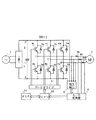
図1は、本発明によるインバータ装置の一実施形態で、図において、1は交流電源、2は整流回路、3は平滑用のコンデンサ、4u〜4zはインバータを構成する半導体スイッチング素子、5u〜5zはフリーホィールダイオード、6u〜6wは電流検出器、7は負荷となる電動機(ここでは3相誘導電動機)、8は電圧検出手段、9はA/D変換器、10は制御用のCPU、11はゲートドライブ回路、それに12はメモリである。
【0021】
まず、インバータ主回路部について説明する。
ここで、このインバータ主回路部とは、通例、半導体スイッチング素子4u〜4z、それにフリーホィールダイオード5u〜5zからなる部分を指すが、整流回路2とコンデンサ3も含めて呼ぶこともある。
【0022】
交流電源1から供給された3相交流電力は、整流回路2により直流電力に変換される。
なお、ここでは、整流回路2として、ダイオード整流回路が示してあるが、スイッチング素子からなるコンバータ回路を用いてもよい。
整流回路2から出力される直流電圧は、コンデンサ3により平滑化され、インバータ主回路部に供給される。
【0023】
インバータ主回路部は、図示のように、直列接続した2個のIGBTからなる部分(これをアームと呼ぶ)を3相分備えている。
そして、各アームの中で、上アーム側のIGBT4u、4v、4wのコレクタ端子は夫々直流電圧の正側Pに接続され、下アーム側のIGBT4x、4y、4zのエミッタ端子は直流電圧の負側Nに接続されている。
【0024】
さらに、上アーム側のIGBT4u〜4wと下アーム側のIGBT4x〜4zには、各々フリーホィールダイオード5u〜5zが逆並列接続され、これにより三相インバータ主回路部を形成している。
そして、各相のアームの中点U、V、Wを交流出力端子とし、これらに電動機7が接続され、インバータ装置の負荷となっている。
【0025】
次に、インバータ制御回路について説明する。
ここで、このインバータ制御回路とは、電流検出器6u〜6wと電圧検出回路8、A/D変換器9、CPU10、ゲートドライブ回路11、それにメモリ12からなる部分のことを指す。
【0026】
電圧検出回路8は、平滑回路3で平滑化したインバータの直流電源電圧と、3相インバータ主回路部の各相出力端子の電圧レベルを検出し、電流検出器6u、6v、6wは、夫々3相インバータ主回路部の各相出力線の電流を検出する。 そして、これら電圧検出回路8で検出した信号と、電流検出器6u、6v、6wで検出した信号は、夫々A/D変換器9に入力され、アナログ信号からディジタル信号に変換されてCPU10に供給される。
【0027】
このとき、電圧検出回路8では、ある基準電位から、直流電源電圧の正側Pと負側N、それに3相の各出力端子の電圧を測定する。従って、例えば直流電源電圧の負側Nを基準電位とすると、直流電圧の負側Nは常に0Vとなるため、他の4種の電位を測定すればよいことになる。
【0028】
なお、実際のインバータ装置では、直流電圧Vdc が、例えば200V以上野かなり高い電圧になるため、これらの値を直接電圧検出回路8に取り込むのは非現実的であり、このため、各電圧を抵抗などで分圧して基準電位と比較する方法が、主として用いられる。
【0029】
CPU10は、インバータが運転中、A/D変換器9から供給される信号を用い、電動機7の電気的定数を演算(演算処理については後述)し、演算結果をメモリ12に書替記憶する処理と、このメモリ12から読出した電気的定数を用い、電動機7の性能を最大限に引き出すことができるようなゲートパルスを作成し、ゲートドライブ回路11によりインバータ主回路部のスイッチング素子を駆動する処理とを並行して、夫々所定の頻度で逐次、実行するようにプログラム構成してある。
【0030】
次に、この実施形態の各部の動作について説明する。
まず、図2により、この実施形態で半導体スイッチング素子の制御に用いられているパルス幅変調(PWM)方式について説明する。
なお、実用上は、多パルス(マルチパルス)幅変調方式とするのが通例なので、この実施形態でも、多パルス幅変調方式の場合について説明する。
【0031】
この多パルス幅変調方式とは、出力交流基本波の半サイクルの間に2個以上のパルスを発生させ、それらのパルス幅の調整により出力の基本成分の制御が得られると共に、高調波成分の低減が図れるという特長を持つ方式のことで、インバータ主回路部の制御方式として広く用いられている一般的なものである。
【0032】
この図2において、まず、同図(1)〜(3)は3相交流出力電圧のU、V、Wの各相における基本波の波形を示したもので、図示のように、各基本波は夫々正弦波形をなしていて、相間で2/3πづつ位相がずれている。
【0033】
次に、これら正弦波からなる基本波成分と、一般に三角波信号が用いられている搬送波成分とを、図2(4)に示すように比較し、例えば図2(5)に示すように、基本波成分が三角波信号よりも大きくなっている期間だけ正電圧になるパルスを生成する。
【0034】
そして、この図2(5)に示すパルスを用いて、U、V、Wの各相上下アームの半導体スイッチング素子をオン/オフさせることにより、3相交流出力が滑らかな正弦波に近づけられるようにしているのである。
【0035】
なお、ここでは、パルスの生成方法として、基本波成分と三角波の搬送波成分とを比較する方法について説明したが、本発明がこのパルス生成方法に依存しないことは明らかであり、従って、他のパルス生成方法によっても実施することができる。
【0036】
次に、上記したCPU11による電動機の電気的定数の演算処理について説明する。
なお、インバータ主回路部では、出力交流の基本波の位相に応じて、主な電流の経路が種々に変化する。そこで、以下、この経路の変化毎に説明する。
【0037】
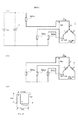
まず、図3は、インバータ主回路部と、これに接続された電動機7からなる部分だけを示した図で、ここで、13は直流電圧源で、例えば整流回路2から出力され、コンデンサ3で平滑化された直流電圧Vdc を発生する回路を等価的に表わしたものである。
【0038】
この図3において、上アームのIGBT4u〜4wと、下アームのIGBT4x〜4zには、各々フリーホィールダイオード5u〜5zが逆並列接続され、これにより3相のインバータ主回路部を形成し、その出力は、負荷となる電動機7に供給される。
ここで、この電動機7の電気的定数については、その1次抵抗成分r1だけが示してある。
【0039】
いま、この図3のインバータ主回路部の各IGBTを、図2(5)に示すゲートパルスで駆動したとすると、図4と図5に示すように、基本波の位相θに応じて電流経路が変化する。ここで、図4は、位相θ=0のときの電流経路と相間電圧を示した図で、図5は、位相θ=π/2のときの電流経路と相間電圧を示した図である。
【0040】
図2において、位相θ=0のときは、U相の電流Iuは0、V相の電流IvはW相の電流Iwと同じの或る値になるが、流れる方向は反対になる。
このため、位相θ=0においては、W相上アームのIGBT4wとV相下アームのIGBT4yだけがオンするので、電流の経路は図4(1)に示すようになり、電流Iwと電流Iv(=−Iw)が流れる。なお、図4では、電流の流れない部分の回路は省略してある。
【0041】
この図4(1)で、抵抗R4wはIGBT4wのオン抵抗を、そして抵抗R4yはIGBT4yのオン抵抗を、夫々表わしており、従って、オン状態のW相上アームのIGBTと、V相下アームのIGBTには、各々オン電圧ΔVw1(=R4w×Iw)、ΔVy1(=R4y×Iv)が発生する。
【0042】
従って、電動機に印加される電圧成分Vwv(V相出力端子に対するW相出力端子の電位)は、直流電源電圧Vdc より、オンしている2個のIGBTのオン電圧分ΔVa (=ΔVw1+ΔVy1)だけ低下してしまうことになる。
【0043】
次に、IGBT4wがオフされると環流電流が生じるが、このときの電流経路は、図4(2)に示すように、W相下アームのフリーホィールダイオード5zがオンして、これが電流経路になる。
ここで、抵抗R4zはフリーホィールダイオード5zのオン抵抗であり、従って、ここにもオン電圧ΔVz2(=R4z×Iw)が現れる。
【0044】
つまり、電圧成分Vwvは、電源電圧Vdc とは切り離されているが、V相下アームのIGBT4yのオン電圧ΔVy1と、W相下アームのフリーホィールダイオード5zのオン電圧ΔVz2の和のオン電圧分ΔVb (=ΔVy1+ΔVz2)だけ低い電圧となる。
【0045】
従って、電圧成分Vwvの時間による変化は、図4(3)に示すようになる。
ここで、Tcは、搬送波(図2(4)の三角波)の周期であり、ΔVon1は、図4(1)のとき、抵抗R4wと抵抗R4yに電流Iwが流れたことによる電圧降下分で、ΔVon2は、図4(2)のとき、抵抗R4wと抵抗R5zに電流Iwが流れたことによる電圧降下分である。
【0046】
ところで、従来技術では、上記したように、期間Tc/2における電動機7の一次抵抗r1は、数1式で示したように、平均電圧Vave を電動機電流Iで割ることにより求めている。
【0047】
しかし、本発明では、従来技術とは異なり、平均電圧Vave として、半導体スイッチング素子のオン電圧成分を補正した値を用い、次の数3式により電動機7の一次抵抗r1を計算するのである。
【0048】
【数3】
従って、本発明では、この実施形態から明らかなように、数3式の分子の値を平均電圧Vave としていることになる。
なお、このとき半導体スイッチング素子のオン期間Ton が、期間Tc/2に対して十分に大きく、且つ直流電源電圧Vdc が極めて大きい場合には、電圧分ΔVa と電圧分ΔVb からなるる補正項は無視できるようになるが、実用的なレベル範囲では、これらの補正項は無視できない。
【0050】
何故なら、現状のパワーデバイスのオン電圧は、例えばIGBTについてみた場合、コレクタ・エミッタ間飽和電圧Vce(sat)で示されているが、これは数Vオーダーにもなるからである。
他方、このことは、本発明では補正が行われる結果、少なくとも10%は精度改善が可能なことを意味する。
【0051】
次に、位相θがπ/2の場合について、図5を用いて説明する。
図2において、位相θ=π/2の場合、U相電流が最大になり、V相電流とW相電流は同じ大きさで、ともにU相電流と逆向きとなる。
この状態におけるインバータのスイッチングモードは、U相上アームのIGBT4uと、V相下アームのIGBT4y、それにW相下アームのIGBT4zがオンとなるので、図5(1)のような電流経路となる。
【0052】
また、この状態でU相上アームのIGBT4uがオフすると、U相下アームのフリーホィールダイオード5xがオンするので、図5(2)に示す環流モードとなる。
従って、このときのV相出力端子とU相出力端子の間の電圧Vuvは図5(3)のようになり、平均電圧は、次の数4式の分子のようになる。
【0053】
【数4】
ここで、ΔVc はIGBT4uのオン電圧とIGBT4yのオン電圧の和の電圧分で、ΔVd はフリーホィールダイオード5xのオン電圧とIGBT4yのオン電圧の和の電圧分である。
従って、CPU11は、以上のようにして電動機7の電気的定数のうちの1次抵抗r1を逐次演算し、演算結果をメモリ12に更新記憶してゆくことになる。
【0055】
ここで、これら数3式と数4式から明らかなように、位相によりインバータ主回路部の電流経路が変わり、演算に考慮しなければならない半導体素子(スイッチング素子とフリーホィールダイオード)が違ってしまう。
一方、個々の半導体素子について、オン電圧が全て揃っていて、同じ変化をするなどは、事実上望むべくもないことから、予めオン電圧を想定し、設定しておいたのでは、とても精度は保てない。
【0056】
しかるに、この本発明の実施形態によれば、インバータ装置が運転中は、CPU11が逐次オン電圧を測定し、順次新たな数値がメモリ12に記憶されてゆくので、各半導体素子の運転中での実際のオン電圧に基づいて、電動機7の運転中での実際の1次抵抗が演算されることになるので、容易に高精度のオートチューニングを保つことができる。
【0057】
ところで、以上の実施形態のままでは、インバータ装置が運転を開始した時点では、まだ電動機7の1次抵抗が演算されていないことになり、始動時でのインバータ装置の適切な制御に支障が生じてしまう。
そこで、このため、本発明の実施形態としては、インバータ装置が運転を停止したときは、そのときメモリ12に記憶されていたデータが、次にインバータ装置が運転を開始するまで保持されるように構成する必要がある。
【0058】
または、別途、インバータ装置の制御に必要な標準的なデータをテーブルとして保持させてき、始動後、所定の電気的定数が演算され、メモリ12にデータが格納された時点で、メモリ12のデータによる制御に切換えられるように構成してもよい。
【0059】
ところで、この実施形態による1次抵抗r1の演算式は、上記したように、位相に応じて演算内容が変化する。従って、上記数3式と数4式については、位相について一般化した次の数5式で表わすことができる。
【0060】
【数5】
ここで、この数5式の分母のβ(θ)は、位相θがπ/3と2π/3のときβ=1となり、位相θがπ/2のときβ=3/4となるような関数を表わし、ΔVr は代表値として選んだIGBTのオン電圧の2倍の値であり、ΔVs は代表値として選んだIGBTとフリーホィールダイオードのオン電圧の和を表わす。
【0062】
次に、この実施形態における個々の半導体素子のオン電圧を測定する方法について、図6により説明する。なお、ここでは、フリーホィールダイオードをFWDと記す。
この図6において、まず、同図(1)は、半導体素子のオン電圧測定時におけるスイッチングモードの説明図である。
【0063】
この図6(1)には、上アームのIGBT(A)と下アームのIGBT(B)、それにIGBT(A)と逆並列接続されたFWD(A)と、IGBT(B)に逆並列接続されたFWD(B)からなる1相分のアームが示されており、さらにIGBT(A)のコレクタ端子は正側電源Pに接続され、IGBT(B)のエミッタ端子は負側電源Nに接続されており、出力端子となる両方のIGBTの接続点がUとして示されている。
【0064】
そこで、この図6(1)の回路において、P−N間に直流電源を接続し、U点には負荷を接続した上で、IGBT(A)とIGBT(B)の各ゲートに、図6(2)に示すパルスを入力したとすると、各スイッチングモードにおける電流経路は、太い実線で示すモード▲1▼と、太い波線で示すモード▲2▼、細い実線で示すモード▲3▼、細い波線で示すモード▲4▼の順に変化する。
【0065】
ここで、まずモード▲1▼では、IGBT(A)がオンし、IGBT(B)はオフなので、この場合には、太い実線で示すように、電源からIGBT(A)を経由してU点から負荷に電流が流れる。
従って、このときは、P点の電位からU点の電位を差し引いた電圧がIGBT(A)のオン電圧となる。
【0066】
次に、モード▲2▼では、IGBT(A)とIGBT(B)の双方がオフなので、太い波線で示すように、FWD(B)に循環電流か流れるため、U点の電位からP点の電位を差し引いた電圧がFWD(B)のオン電圧となる。
【0067】
また、モード▲3▼では、IGBT(A)はオフで、IGBT(B)がオンするので、この場合には、細い実線で示すように、負荷からU点を通り、IGBT(B)を経由して電源に電流が流れる。
従って、このときは、U点の電位からN点の電位を差し引いた電圧がIGBT(B)のオン電圧となる。
【0068】
そして、モード▲4▼では、IGBT(A)とIGBT(B)の双方がオフなので、細い波線で示すように、FWD(A)に循環電流か流れるため、P点の電位からU点の電位を差し引いた電圧がFWD(A)のオン電圧となる。
従って、これらを纏めると、被測定素子と測定端子の関係は図6(3)に示すようになる。ここで、Vn はP点の電位で、Vp はP点の電位、そしてVu はU点の電位である。
【0069】
このように、各スイッチングモード毎に直流電源の正側P点の電位Vp 及び負側N点の電位Vn 、それに出力端子U点の電位Vu を測定することにより、各半導体素子のオン電圧を個別に測定することができる。
【0070】
そこで、CPU11は、自らが制御しているインバータ主回路部のスイッチングモードに応じて、電圧検出回路8によりインバータ主回路部の各点から検出した電圧をA/D変換器9を介して取込み、図6(3)に従って演算し、各半導体素子のオン電圧を個別に測定し、この測定結果に基づいて電動機7の1次抵抗r1を演算し、それをメモリ12に順次更新記憶してゆく処理を実行する。
【0071】
従って、この実施形態によれば、ほとんど実時間による各半導体素子のオン電圧に基づいて電動機7の1次抵抗r1が演算されるので、インバータ装置運転中での各部の温度変化の影響を受ける虞れがなく、極めて高精度のチューニングが可能になり、オートチューニングによる常に的確な交流電動機の制御を容易に得ることができる。
【0072】
ところで、このようなインバータ装置においては、インバータ主回路部の同一相の上アームと下アームが同時にオンすると、電源短絡状態になってしまうので、上下アームのスイッチング時間にデッドタイムを設定して制御するのが一般的である。
しかして、このデッドタイムを設けた場合には、オートチューニングに誤差が生じてしまう。
【0073】
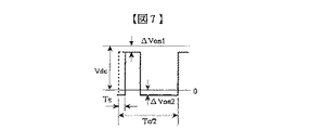
そこで、このオートチューニングにおけるデッドタイムを補正するようにした本発明の実施形態における演算内容について、図7により説明する。
この図7において、Ts はデッドタイムを設けたことによる遅れ時間であり、従って、図4(3)と図5(3)と異なっている点は、この遅れ時間Ts が存在する点だけである。
【0074】
この遅れ時間Ts は、デッドタイムをΔTd、ゲートドライブ回路11と半導体スイッチング素子のオン時の動作遅れ時間の和をΔTon、ゲートドライブ回路11と半導体スイッチング素子のオフ時の動作遅れ時間の和をΔToff とした場合、これらを組み合わせたもので、次の数6式で表せる。
【0075】
【数6】
そこで、この実施形態では、この遅れ時間Ts を考慮し、上記数5式による演算に代えて、CPU11は、次の数7式により電動機7の1次抵抗r1を演算するのである。
【0077】
【数7】
従って、この実施形態によれば、デッドタイムによる精度の低下が抑えられ、この結果、さらにオートチューニングの精度が向上する。
なお、上記本発明の実施形態では、インバータ主回路部のスイッチング素子としてIGBTを用いた場合について説明したが、バイポーラパワートランジスタやGTO、MOSFETなどの各種のパワースイッチング素子を使用して実施することも勿論可能である。
【0079】
また、上記実施形態では、インバータ装置の基本的構成が2レベルインバータになっている場合について説明したが、3レベル以上のマルチレベルインバータにも適用可能なこともいうまでもない。
【0080】
さらに、上記実施形態では、半導体素子のオン電圧の測定結果を電動機の1次抵抗の演算に適用した場合についてだけ説明したが、他の電気的定数の演算にも適用可能であり、いずれの場合でもオートチューニングの精度を向上させることができる。
【0081】
【発明の効果】
本発明によれば、各半導体素子のオン電圧に基づいて、電動機の1次抵抗が演算されることになる。
【0082】
また、この結果、インバータ装置のオートチューニング精度が向上するので、電動機の効率的な運転状態を保つことができる。
また、インバータ主回路部の半導体素子のオン電圧に存在する特性のバラツキの影響を低減することができる。
【図面の簡単な説明】
【図1】本発明によるオートチューニング型インバータ装置の一実施形態を示す回路図である。
【図2】本発明の一実施形態における多パルス幅変調による制御動作を説明するための波形図である。
【図3】本発明の一実施形態の動作を説明するための等価回路図である。
【図4】本発明の一実施形態の等価回路における電流経路と相間電圧の一例を示す説明図である。
【図5】本発明の一実施形態の等価回路における電流経路と相間電圧の一例を示す説明図である。
【図6】本発明の一実施形態におけるスイッチングモードの説明図である。
【図7】デッドタイムを考慮した本発明の一実施形態による平均電圧の説明図である。
【図8】従来技術による平均電圧の説明図である。
【符号の説明】
1 3相交流電源
2 整流回路(インバータ装置の順変換部)
3 平滑用コンデンサ
4u〜4z IGBT(インバータ主回路部の半導体スイッチング素子)
5u〜5z フリーホィールダイオード
6u〜6w 電流検出器
7 交流電動機(誘導電動機)
8 電圧検出回路
9 A/D変換器
10 CPU(中央演算装置)
11 ゲートドライブ回路
12 メモリ
13 直流電圧源
R4u〜R4z IGBT4u〜4zのオン抵抗
R5u〜R5z フリーホィールダイオード5u〜5zのオン抵抗[0001]
BACKGROUND OF THE INVENTION
The present invention relates to an inverter device for driving an electric motor.RelatedTo do.
[0002]
[Prior art]
As is well known, according to the inverter device, AC power with variable voltage and variable frequency can be easily supplied, so it is widely used for driving AC motors such as induction motors and greatly contributes to efficient operation by variable speed operation. However, in this case, by controlling the inverter in accordance with the characteristics of the AC motor serving as a load, the performance of the motor can be utilized to the maximum and more efficient operation can be obtained.
[0003]
Therefore, an auto-tuning inverter device that sets a control constant according to the characteristics of the electric motor that is a load and controls the inverter based on the control constant has recently attracted attention.
[0004]
By the way, in order to set the control constant in this auto-tuning inverter device, it is necessary to know in advance the characteristics of the motor that is the load, that is, the so-called motor constant. In this case, in particular, a method for measuring the primary resistance r1 of the induction motor For example, the following method is common.
[0005]
That is, at the output point of the inverter main circuit, a pulse voltage appears as shown in FIG. 8 due to the switching operation of the semiconductor switching element.
Therefore, first, the average voltage Vave is calculated from the DC voltage Vdc between the DC inputs PN of the inverter main circuit and the on-time Ton of the semiconductor switching element according to the equation (1).
Here, Tc is a period of a pulse width modulation carrier wave (details will be described later).
[0006]
[Expression 1]
Next, the primary resistance r1 is calculated from the average voltage Vave and the current I flowing through the electric motor as a load, as shown in
[0008]
[Expression 2]
Here, α (θ) is a coefficient depending on the phase angle θ, and is as follows, for example.
θ = 0 → α (θ) = 2
θ = π / 2 → α (θ) = 1.5
[0010]
In the prior art, the electric constants of the motor such as the primary resistance thus obtained are set in advance in a table or the like and used for controlling the inverter.
As a document disclosing this kind of technology, JP-A-6-98595 can be cited.
[0011]
[Problems to be solved by the invention]
In the above prior art, it cannot be said that sufficient consideration has been given to the electrical constant of the motor that is the load and the accuracy of the forward voltage (ON voltage) present in the various semiconductor elements constituting the inverter main circuit. There was a problem with tuning accuracy.
[0012]
In general, an inverter device supplies an alternating current to an electric motor or the like as a load by turning on (conducting) and turning off (cut off) a plurality of semiconductor switching elements such as IGBTs and GTOs.
Here, the IGBT is an insulated gate bipolar transistor, and the GTO is a gate turn-off thyristor.
[0013]
However, a semiconductor switching element generally does not become a complete conduction state even when it is turned on, and a minute resistance (referred to as an on-resistance) remains. Therefore, an on-voltage (forward order) determined by the product of the on-resistance and the conduction current. The generation of a voltage drop component called voltage is inevitable.
Therefore, not only in the mode in which the circulating current flows, but also in the electric motor as a load, a voltage drop for canceling the on-voltage is always generated.
[0014]
In addition, this on-resistance is dependent on current and temperature, and has the property of changing depending on the magnitude and temperature of the energization current. Furthermore, this property is a freewheel connected in reverse parallel to switching elements such as IGBT and GTO. I also have a diode.
[0015]
In addition, the electrical constant of the electric motor that is the load has temperature dependence, and variations in characteristics among individuals cannot be ignored.
Therefore, in order to hold the electric constant of the electric motor in advance, a large number of data is required according to the above-described various dependencies, and a lot of fine data is required for high-precision holding.
[0016]
However, in the prior art, the electrical constant of the motor that has become a load is calculated from discontinuous data stored in advance in a table or the like, so the tuning accuracy is determined by the interpolation accuracy between the data, A problem arises in maintaining sufficient accuracy.
[0017]
An object of the present invention is to provide an electrical constant of a motor that is a load.EasyMotor control by auto tuningCanAn object of the present invention is to provide such an inverter device.
[0018]
[Means for Solving the Problems]
The object is to provide at least two arms in the inverter main circuit section, which are composed of a series connection circuit of two semiconductor switching elements.Auto tuning methodIn the inverter device ofWhile the inverter main circuit is operating,Means for measuring the forward voltage of the semiconductor switching elementAnd means for sequentially calculating a primary resistance component of the motor connected to the inverter main circuit from the forward voltage;ProvidedAuto tuning is given by the primary resistance component calculated sequentially.Is achieved in this way.
[0019]
Also, the above purpose is to automatically measure the electrical constant of the motor connected to the output.Of auto tuningIn the inverter device, during the operation of the motor, the forward voltage of at least one of the semiconductor switching element and the free wheel diode constituting the arm of the inverter main circuit unit is sequentially measured, and the measured forward voltage is used for the motor.Primary resistance componentCalculate and store calculation resultsSo that auto tuning is given.Even achieved.
[0020]
DETAILED DESCRIPTION OF THE INVENTION
Hereinafter, an inverter device according to the present invention will be described in detail with reference to the illustrated embodiments.
FIG. 1 is an embodiment of an inverter device according to the present invention. In the figure, 1 is an AC power supply, 2 is a rectifier circuit, 3 is a smoothing capacitor, 4u to 4z are semiconductor switching elements constituting the inverter, and 5u to 5z. Is a free wheel diode, 6u to 6w are current detectors, 7 is an electric motor (in this case, a three-phase induction motor), 8 is a voltage detection means, 9 is an A / D converter, 10 is a CPU for control, 11 Is a gate drive circuit, and 12 is a memory.
[0021]
First, the inverter main circuit part will be described.
Here, the inverter main circuit portion usually indicates a portion including the semiconductor switching elements 4u to 4z and the free wheel diodes 5u to 5z, but may be referred to as including the
[0022]
The three-phase AC power supplied from the
Here, although a diode rectifier circuit is shown as the
The DC voltage output from the
[0023]
As shown in the figure, the inverter main circuit section is provided with a portion composed of two IGBTs connected in series (referred to as an arm) for three phases.
In each arm, the collector terminals of the IGBTs 4u, 4v and 4w on the upper arm side are respectively connected to the positive side P of the DC voltage, and the emitter terminals of the
[0024]
Further, free wheel diodes 5u to 5z are connected in reverse parallel to the upper arm side IGBTs 4u to 4w and the lower
Then, the midpoints U, V, and W of the arms of each phase are used as AC output terminals, and an
[0025]
Next, the inverter control circuit will be described.
Here, the inverter control circuit refers to a portion including the current detectors 6u to 6w, the
[0026]
The
[0027]
At this time, the
[0028]
Note that in an actual inverter device, the DC voltage Vdc becomes a considerably high voltage of, for example, 200 V or more. Therefore, it is impractical to take these values directly into the
[0029]
The
[0030]
Next, the operation of each part of this embodiment will be described.
First, the pulse width modulation (PWM) method used for controlling the semiconductor switching element in this embodiment will be described with reference to FIG.
In practice, a multi-pulse (multi-pulse) width modulation method is usually used. Therefore, in this embodiment, the case of the multi-pulse width modulation method will be described.
[0031]
In this multi-pulse width modulation method, two or more pulses are generated during the half cycle of the output AC fundamental wave, and the basic component of the output can be controlled by adjusting the pulse width, and the harmonic component This is a system that has the feature that it can be reduced, and is a general system widely used as a control system for the inverter main circuit section.
[0032]
In FIG. 2, first, (1) to (3) show the waveforms of the fundamental waves in the U, V, and W phases of the three-phase alternating current output voltage. Each have a sinusoidal waveform, and the phase is shifted by 2 / 3π between the phases.
[0033]
Next, the fundamental wave component composed of these sine waves and the carrier wave component in which a triangular wave signal is generally used are compared as shown in FIG. 2 (4). For example, as shown in FIG. A pulse that generates a positive voltage only during a period when the wave component is larger than the triangular wave signal is generated.
[0034]
Then, by using the pulses shown in FIG. 2 (5) to turn on / off the semiconductor switching elements of the upper and lower arms of U, V, and W, the three-phase AC output can be brought close to a smooth sine wave. It is.
[0035]
Here, as a pulse generation method, the method of comparing the fundamental wave component and the triangular wave carrier component has been described. However, it is clear that the present invention does not depend on this pulse generation method, and therefore other pulses are generated. It can also be implemented by the generation method.
[0036]
Next, the electric constant calculation processing of the electric motor by the
Note that, in the inverter main circuit section, the main current path changes variously according to the phase of the fundamental wave of the output AC. Therefore, hereinafter, each change of the route will be described.
[0037]
First, FIG. 3 is a diagram showing only a part composed of an inverter main circuit part and an
[0038]
In FIG. 3, free wheel diodes 5u to 5z are connected in reverse parallel to the upper arm IGBTs 4u to 4w and the
Here, only the primary resistance component r1 of the electric constant of the
[0039]
Now, assuming that each IGBT of the inverter main circuit portion of FIG. 3 is driven by the gate pulse shown in FIG. 2 (5), as shown in FIG. 4 and FIG. Changes. Here, FIG. 4 is a diagram showing a current path and an interphase voltage when the phase θ = 0, and FIG. 5 is a diagram showing a current path and an interphase voltage when the phase θ = π / 2.
[0040]
In FIG. 2, when the phase θ = 0, the U-phase current Iu is 0 and the V-phase current Iv is the same value as the W-phase current Iw, but the flow direction is opposite.
Therefore, in the phase θ = 0, only the
[0041]
In FIG. 4 (1), the resistor R4w represents the on-resistance of the
[0042]
Therefore, the voltage component Vwv applied to the motor (the potential of the W-phase output terminal with respect to the V-phase output terminal) is reduced by the on-voltage ΔVa (= ΔVw1 + ΔVy1) of the two IGBTs that are turned on from the DC power supply voltage Vdc. Will end up.
[0043]
Next, when the
Here, the resistor R4z is the on-resistance of the free wheel diode 5z, and therefore the on-voltage ΔVz2 (= R4z × Iw) also appears here.
[0044]
That is, the voltage component Vwv is separated from the power supply voltage Vdc, but the on-voltage component ΔVb that is the sum of the on-voltage ΔVy1 of the IGBT 4y of the V-phase lower arm and the on-voltage ΔVz2 of the freewheel diode 5z of the W-phase lower arm. The voltage becomes lower by (= ΔVy1 + ΔVz2).
[0045]
Therefore, the change with time of the voltage component Vwv is as shown in FIG.
Here, Tc is the period of the carrier wave (triangular wave in FIG. 2 (4)), and ΔVon1 is the voltage drop due to the current Iw flowing through the resistors R4w and R4y in FIG. ΔVon2 is a voltage drop due to the current Iw flowing through the resistors R4w and R5z in FIG. 4 (2).
[0046]
By the way, in the prior art, as described above, the primary resistance r1 of the
[0047]
However, in the present invention, unlike the prior art, the primary resistance r1 of the
[0048]
[Equation 3]
Therefore, in the present invention, as is apparent from this embodiment, the value of the numerator in the
At this time, when the on-period Ton of the semiconductor switching element is sufficiently longer than the period Tc / 2 and the DC power supply voltage Vdc is extremely large, the correction term composed of the voltage component ΔVa and the voltage component ΔVb is ignored. In the practical level range, these correction terms cannot be ignored.
[0050]
This is because the on-voltage of the current power device is indicated by the collector-emitter saturation voltage Vce (sat) in the case of an IGBT, for example, which is on the order of several volts.
On the other hand, this means that the accuracy can be improved by at least 10% as a result of the correction in the present invention.
[0051]
Next, the case where the phase θ is π / 2 will be described with reference to FIG.
In FIG. 2, when the phase θ = π / 2, the U-phase current becomes maximum, the V-phase current and the W-phase current have the same magnitude, and both are opposite to the U-phase current.
The switching mode of the inverter in this state is a current path as shown in FIG. 5 (1) because the U-phase upper arm IGBT 4u, the V-phase lower arm IGBT 4y, and the W-phase
[0052]
Further, when the IGBT 4u of the U-phase upper arm is turned off in this state, the free wheel diode 5x of the U-phase lower arm is turned on, so that the circulation mode shown in FIG.
Accordingly, the voltage Vuv between the V-phase output terminal and the U-phase output terminal at this time is as shown in FIG. 5 (3), and the average voltage is as a numerator of the following equation (4).
[0053]
[Expression 4]
Here, ΔVc is the sum of the on-voltage of the IGBT 4u and the on-voltage of the IGBT 4y, and ΔVd is the sum of the on-voltage of the free wheel diode 5x and the on-voltage of the IGBT 4y.
Therefore, the
[0055]
Here, as is clear from these equations (3) and (4), the current path of the inverter main circuit section changes depending on the phase, and the semiconductor elements (switching elements and freewheel diodes) that must be taken into consideration in the calculation are different. .
On the other hand, for each semiconductor element, it is virtually impossible to have the same on-state voltage and the same change, so assuming the on-voltage in advance and setting it is very accurate. I can't keep it.
[0056]
However, according to this embodiment of the present invention, while the inverter device is in operation, the
[0057]
By the way, with the above embodiment, when the inverter device starts operation, the primary resistance of the
Therefore, as an embodiment of the present invention, when the inverter device stops operating, the data stored in the
[0058]
Alternatively, standard data necessary for controlling the inverter device is separately held as a table, and after starting, a predetermined electrical constant is calculated and stored in the
[0059]
By the way, as described above, the calculation content of the primary resistance r1 according to this embodiment varies depending on the phase. Therefore, the
[0060]
[Equation 5]
Here, β (θ) of the denominator of
[0062]
Next, a method for measuring the ON voltage of each semiconductor element in this embodiment will be described with reference to FIG. Here, the free wheel diode is referred to as FWD.
In FIG. 6, first, FIG. 1A is an explanatory diagram of a switching mode at the time of measuring an on-voltage of a semiconductor element.
[0063]
In FIG. 6 (1), the upper arm IGBT (A), the lower arm IGBT (B), the FWD (A) connected in reverse parallel to the IGBT (A), and the IGBT (B) connected in reverse parallel The one-phase arm of FWD (B) is shown, the collector terminal of IGBT (A) is connected to the positive power supply P, and the emitter terminal of IGBT (B) is connected to the negative power supply N The connection point of both IGBTs serving as output terminals is indicated as U.
[0064]
Therefore, in the circuit of FIG. 6 (1), a DC power source is connected between P and N, a load is connected to the U point, and each gate of IGBT (A) and IGBT (B) is connected to FIG. If the pulse shown in (2) is input, the current path in each switching mode is as follows: mode (1) indicated by a thick solid line; mode (2) indicated by a thick wavy line; mode (3) indicated by a thin solid line; The mode changes in the order of mode (4).
[0065]
Here, in the mode (1), the IGBT (A) is on and the IGBT (B) is off. In this case, as shown by the thick solid line, the U point is connected from the power source via the IGBT (A). Current flows from the load to the load.
Therefore, at this time, a voltage obtained by subtracting the potential at the point U from the potential at the point P becomes the ON voltage of the IGBT (A).
[0066]
Next, in mode (2), since both IGBT (A) and IGBT (B) are off, as shown by the thick wavy line, the circulating current flows through FWD (B). The voltage obtained by subtracting the potential is the ON voltage of FWD (B).
[0067]
In mode (3), IGBT (A) is off and IGBT (B) is on. In this case, as indicated by a thin solid line, it passes through point U from the load and passes through IGBT (B). Current flows through the power supply.
Accordingly, at this time, a voltage obtained by subtracting the potential at the N point from the potential at the U point becomes the ON voltage of the IGBT (B).
[0068]
In mode (4), since both IGBT (A) and IGBT (B) are off, the circulating current flows through FWD (A) as shown by the thin wavy line, so the potential at point U from the potential at point P. The voltage obtained by subtracting is the ON voltage of FWD (A).
Therefore, when these are summarized, the relationship between the element to be measured and the measurement terminal is as shown in FIG. Here, Vn is the potential at point P, Vp is the potential at point P, and Vu is the potential at point U.
[0069]
In this way, by measuring the potential Vp at the positive P point and the potential Vn at the negative N point of the DC power source and the potential Vu at the output terminal U for each switching mode, the on-voltage of each semiconductor element is individually determined. Can be measured.
[0070]
Therefore, the
[0071]
Therefore, according to this embodiment, since the primary resistance r1 of the
[0072]
By the way, in such an inverter device, if the upper and lower arms of the same phase of the inverter main circuit section are turned on at the same time, the power supply is short-circuited. It is common to do.
Therefore, when this dead time is provided, an error occurs in auto-tuning.
[0073]
Therefore, the calculation contents in the embodiment of the present invention in which the dead time in the auto tuning is corrected will be described with reference to FIG.
In FIG. 7, Ts is a delay time due to the provision of a dead time. Therefore, the only difference from FIGS. 4 (3) and 5 (3) is that this delay time Ts exists. .
[0074]
The delay time Ts is the dead time ΔTd, the sum of the operation delay times when the
[0075]
[Formula 6]
Therefore, in this embodiment, in consideration of the delay time Ts, the
[0077]
[Expression 7]
Therefore, according to this embodiment, a decrease in accuracy due to dead time is suppressed, and as a result, the accuracy of auto-tuning is further improved.
In the above-described embodiment of the present invention, the case of using the IGBT as the switching element of the inverter main circuit portion has been described. However, various power switching elements such as a bipolar power transistor, a GTO, and a MOSFET may be used. Of course it is possible.
[0079]
Moreover, although the case where the basic configuration of the inverter device is a two-level inverter has been described in the above embodiment, it goes without saying that the present invention can also be applied to a multi-level inverter having three or more levels.
[0080]
Furthermore, in the above-described embodiment, only the case where the measurement result of the on-voltage of the semiconductor element is applied to the calculation of the primary resistance of the electric motor has been described. But auto tuning accuracy can be improved.
[0081]
【The invention's effect】
According to the present invention,eachSemiconductor elementOnElectric based on voltageMachineThe primary resistance is to be calculatedThe
[0082]
As a result, the auto tuning accuracy of the inverter deviceForSo that the electric motorEffect ofEfficient driving statuskeepbe able to.
Also,The influence of characteristic variations on the on-state voltage of the semiconductor element in the inverter main circuitReductioncan do.
[Brief description of the drawings]
FIG. 1 is a circuit diagram showing an embodiment of an auto-tuning inverter device according to the present invention.
FIG. 2 is a waveform diagram for explaining a control operation by multi-pulse width modulation in one embodiment of the present invention.
FIG. 3 is an equivalent circuit diagram for explaining the operation of the embodiment of the present invention.
FIG. 4 is an explanatory diagram illustrating an example of a current path and an interphase voltage in an equivalent circuit according to an embodiment of the present invention.
FIG. 5 is an explanatory diagram illustrating an example of a current path and an interphase voltage in an equivalent circuit according to an embodiment of the present invention.
FIG. 6 is an explanatory diagram of a switching mode in an embodiment of the present invention.
FIG. 7 is an explanatory diagram of an average voltage according to an embodiment of the present invention in consideration of dead time.
FIG. 8 is an explanatory diagram of an average voltage according to the prior art.
[Explanation of symbols]
1 3-phase AC power supply
2 Rectifier circuit (forward conversion part of inverter device)
3 Smoothing capacitor
4u-4z IGBT (Semiconductor switching element of inverter main circuit)
5u-5z freewheel diode
6u-6w current detector
7 AC motor (induction motor)
8 Voltage detection circuit
9 A / D converter
10 CPU (Central Processing Unit)
11 Gate drive circuit
12 memory
13 DC voltage source
R4u to R4z IGBT4u to 4z on-resistance
R5u to R5z Free-wheel diode 5u to 5z on-resistance
Claims (4)
前記インバータ主回路部が動作中、逐次、前記半導体スイッチング素子の順電圧を測定する手段と、
前記順電圧から前記インバータ主回路部に接続されている電動機の一次抵抗成分を逐次計算する手段とを設け、
前記逐次計算される一次抵抗成分によりオートチューニングが与えられるように構成したことを特徴とするインバータ装置。In an auto-tuning type inverter device having an arm composed of a series connection circuit of two semiconductor switching elements and having at least two arms in the inverter main circuit part,
Means for sequentially measuring a forward voltage of the semiconductor switching element during operation of the inverter main circuit unit ;
Means for sequentially calculating a primary resistance component of an electric motor connected to the inverter main circuit unit from the forward voltage ;
Inverter apparatus characterized by being configured to so that automatic tuning is provided by the primary resistance component wherein the sequentially computed.
前記半導体スイッチング素子が、前記半導体スイッチング素子に逆並列接続されたフリーホィールダイオードを有し、
前記半導体スイッチング素子の順電圧を測定する手段が、前記フリーホィールダイオードの順電圧を測定する手段を備えていることを特徴とするインバータ装置。The inverter device according to claim 1,
The semiconductor switching element has a free wheel diode connected in reverse parallel to the semiconductor switching element;
An inverter device, wherein the means for measuring the forward voltage of the semiconductor switching element comprises means for measuring the forward voltage of the free wheel diode.
前記電動機が運転中、インバータ主回路部のアームを構成する半導体スイッチング素子とフリーホィールダイオードの少なくとも一方の順電圧を逐次測定し、測定した順電圧を用いて前記電動機の一次抵抗成分を演算し、演算結果を記憶保持してオートチューニングが与えられるように構成したことを特徴とするインバータ装置。In the inverter device of the system that automatically measures the electrical constant of the motor connected to the output and performs auto tuning ,
While the motor is in operation, the forward voltage of at least one of the semiconductor switching element and the free wheel diode constituting the arm of the inverter main circuit unit is sequentially measured, and the primary resistance component of the motor is calculated using the measured forward voltage, inverter apparatus characterized by being configured to so that given autotuning operation result stored and held.
前記電気的定数の自動測定に、前記半導体スイッチング素子の制御に設定されているデッドタイムが考慮されるように構成したことを特徴とするインバータ装置。In the inverter device according to claim 3,
An inverter device configured to take into account a dead time set in the control of the semiconductor switching element in the automatic measurement of the electrical constant.
Priority Applications (1)
| Application Number | Priority Date | Filing Date | Title |
|---|---|---|---|
| JP35662598A JP3774329B2 (en) | 1998-12-15 | 1998-12-15 | Inverter device |
Applications Claiming Priority (1)
| Application Number | Priority Date | Filing Date | Title |
|---|---|---|---|
| JP35662598A JP3774329B2 (en) | 1998-12-15 | 1998-12-15 | Inverter device |
Publications (3)
| Publication Number | Publication Date |
|---|---|
| JP2000184732A JP2000184732A (en) | 2000-06-30 |
| JP2000184732A5 JP2000184732A5 (en) | 2004-12-24 |
| JP3774329B2 true JP3774329B2 (en) | 2006-05-10 |
Family
ID=18449970
Family Applications (1)
| Application Number | Title | Priority Date | Filing Date |
|---|---|---|---|
| JP35662598A Expired - Fee Related JP3774329B2 (en) | 1998-12-15 | 1998-12-15 | Inverter device |
Country Status (1)
| Country | Link |
|---|---|
| JP (1) | JP3774329B2 (en) |
Cited By (1)
| Publication number | Priority date | Publication date | Assignee | Title |
|---|---|---|---|---|
| CN108631684A (en) * | 2017-03-24 | 2018-10-09 | 三菱电机株式会社 | The control device of AC rotary motor |
Families Citing this family (5)
| Publication number | Priority date | Publication date | Assignee | Title |
|---|---|---|---|---|
| JP4678119B2 (en) * | 2001-04-13 | 2011-04-27 | 三菱電機株式会社 | Power converter |
| JP4782525B2 (en) * | 2005-09-30 | 2011-09-28 | 日本電産サーボ株式会社 | Stepping motor drive device |
| JP4913661B2 (en) * | 2007-04-26 | 2012-04-11 | ルネサスエレクトロニクス株式会社 | Inverter device and semiconductor device used therefor. |
| JP5396754B2 (en) * | 2008-06-23 | 2014-01-22 | パナソニック株式会社 | Output estimation device |
| KR101300305B1 (en) * | 2012-04-13 | 2013-08-28 | 엘에스산전 주식회사 | Method for detecting motor parameter in inverter |
-
1998
- 1998-12-15 JP JP35662598A patent/JP3774329B2/en not_active Expired - Fee Related
Cited By (2)
| Publication number | Priority date | Publication date | Assignee | Title |
|---|---|---|---|---|
| CN108631684A (en) * | 2017-03-24 | 2018-10-09 | 三菱电机株式会社 | The control device of AC rotary motor |
| CN108631684B (en) * | 2017-03-24 | 2022-02-11 | 三菱电机株式会社 | Control device for AC rotating machine |
Also Published As
| Publication number | Publication date |
|---|---|
| JP2000184732A (en) | 2000-06-30 |
Similar Documents
| Publication | Publication Date | Title |
|---|---|---|
| US9595889B2 (en) | System and method for single-phase and three-phase current determination in power converters and inverters | |
| JP4985395B2 (en) | Current control device and current offset correction method thereof | |
| CN110323991B (en) | Power module and method for providing multiphase current to multiphase load | |
| JP5026553B2 (en) | Motor drive device having function of dynamically switching conversion operation mode of AC / DC converter | |
| KR20060103552A (en) | Inverter control method and apparatus thereof | |
| JP4031965B2 (en) | Electric motor control device | |
| JP3774329B2 (en) | Inverter device | |
| RU2664591C1 (en) | Method of electric power control and electric power control device | |
| WO2021014666A1 (en) | Current measurement unit and power conversion device | |
| JP3786142B2 (en) | Inverter device | |
| Joshi et al. | Base/gate drive suppression of inactive power devices of a voltage-fed inverter and precision synthesis of AC voltage and DC link current waves | |
| JP2020048360A (en) | Motor control device, motor system, and inverter control method | |
| JP5191152B2 (en) | Motor drive device | |
| JPH02146963A (en) | Controller for voltage type pwm inverter | |
| JP6522227B2 (en) | Converter circuit, inverter circuit and power converter for air conditioner | |
| WO2020012787A1 (en) | Converter device, control signal specification method, and program | |
| JP5895704B2 (en) | Power converter | |
| CN113615077A (en) | Motor control device, motor system, and motor control method | |
| JP3968563B2 (en) | Current detector for voltage type PWM inverter | |
| KR100210449B1 (en) | The power voltage zero-crossing detecting and phase determining method of induction motor driving system using pwm inverter | |
| JP4375506B2 (en) | Inverter device and current limiting method thereof | |
| JPH10174443A (en) | Dc power supply device | |
| KR100202577B1 (en) | Sensorless bldc motor control method and apparatus | |
| JP2022143053A (en) | Power conversion device and washing machine including the same | |
| WO2020012803A1 (en) | Converter device, control signal generation method, and program |
Legal Events
| Date | Code | Title | Description |
|---|---|---|---|
| A521 | Written amendment |
Free format text: JAPANESE INTERMEDIATE CODE: A523 Effective date: 20040128 |
|
| A621 | Written request for application examination |
Free format text: JAPANESE INTERMEDIATE CODE: A621 Effective date: 20040128 |
|
| A711 | Notification of change in applicant |
Free format text: JAPANESE INTERMEDIATE CODE: A712 Effective date: 20040128 |
|
| A977 | Report on retrieval |
Free format text: JAPANESE INTERMEDIATE CODE: A971007 Effective date: 20050930 |
|
| A131 | Notification of reasons for refusal |
Free format text: JAPANESE INTERMEDIATE CODE: A131 Effective date: 20051011 |
|
| A521 | Written amendment |
Free format text: JAPANESE INTERMEDIATE CODE: A523 Effective date: 20051209 |
|
| TRDD | Decision of grant or rejection written | ||
| A01 | Written decision to grant a patent or to grant a registration (utility model) |
Free format text: JAPANESE INTERMEDIATE CODE: A01 Effective date: 20060207 |
|
| A61 | First payment of annual fees (during grant procedure) |
Free format text: JAPANESE INTERMEDIATE CODE: A61 Effective date: 20060217 |
|
| R150 | Certificate of patent or registration of utility model |
Free format text: JAPANESE INTERMEDIATE CODE: R150 |
|
| FPAY | Renewal fee payment (event date is renewal date of database) |
Free format text: PAYMENT UNTIL: 20090224 Year of fee payment: 3 |
|
| FPAY | Renewal fee payment (event date is renewal date of database) |
Free format text: PAYMENT UNTIL: 20100224 Year of fee payment: 4 |
|
| FPAY | Renewal fee payment (event date is renewal date of database) |
Free format text: PAYMENT UNTIL: 20100224 Year of fee payment: 4 |
|
| FPAY | Renewal fee payment (event date is renewal date of database) |
Free format text: PAYMENT UNTIL: 20110224 Year of fee payment: 5 |
|
| FPAY | Renewal fee payment (event date is renewal date of database) |
Free format text: PAYMENT UNTIL: 20120224 Year of fee payment: 6 |
|
| FPAY | Renewal fee payment (event date is renewal date of database) |
Free format text: PAYMENT UNTIL: 20120224 Year of fee payment: 6 |
|
| FPAY | Renewal fee payment (event date is renewal date of database) |
Free format text: PAYMENT UNTIL: 20130224 Year of fee payment: 7 |
|
| FPAY | Renewal fee payment (event date is renewal date of database) |
Free format text: PAYMENT UNTIL: 20130224 Year of fee payment: 7 |
|
| FPAY | Renewal fee payment (event date is renewal date of database) |
Free format text: PAYMENT UNTIL: 20140224 Year of fee payment: 8 |
|
| LAPS | Cancellation because of no payment of annual fees |