JP3766780B2 - Semiconductor laser device - Google Patents
Semiconductor laser device Download PDFInfo
- Publication number
- JP3766780B2 JP3766780B2 JP2000140051A JP2000140051A JP3766780B2 JP 3766780 B2 JP3766780 B2 JP 3766780B2 JP 2000140051 A JP2000140051 A JP 2000140051A JP 2000140051 A JP2000140051 A JP 2000140051A JP 3766780 B2 JP3766780 B2 JP 3766780B2
- Authority
- JP
- Japan
- Prior art keywords
- light
- semiconductor laser
- monitoring
- laser device
- rear end
- Prior art date
- Legal status (The legal status is an assumption and is not a legal conclusion. Google has not performed a legal analysis and makes no representation as to the accuracy of the status listed.)
- Expired - Fee Related
Links
Images


Description
【0001】
【発明の属する技術分野】
この発明は、光ディスク用ピックアップ等に使用される半導体レーザ装置に関する。
【0002】
【従来の技術】
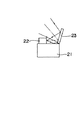
従来、半導体レーザ装置としては、図3に示すものがある。この半導体レーザ装置は、図3に示すように、信号読取のための光源であるレーザダイオード(以下、LDという)22と、上記LD22のレーザ出射光強度をモニタするモニタ用フォトダイオード(以下、PDという)23と、光ディスクのピット情報を含む反射光信号を電気信号に変換する信号受光用PD24とを放熱台21上の所定の位置に夫々固定している。そして、上記LD22, モニタ用PD3および信号受光用PD24の各電極をワイヤボンディングにより所定のリード30に夫々接続した後、キャップ25によって気密封止し、そのキャップ25上にレーザ光を分割,屈折させるホログラム26を固定している。上記LD22,信号受光用PD24は所定の位置に対して取付誤差を有するので、この誤差を補償するようにホログラム26を光学的に調整して最適位置に固定している。
【0003】
【発明が解決しようとする課題】
図4は上記半導体レーザ装置のLD22とモニタ用PD23と信号受光用PD24とが放熱台21に搭載された状態を示している。上記LD22の後端面からの出射光のうち、モニタ用PD23に入射しない光やモニタ用PD23の表面で反射した光がキャップ25(図3に示す)内で乱反射して迷光となる。この迷光が信号受光用PD24の受光部に入射して、ノイズとなるという問題がある。
【0004】
また、図5は図4のV−V線から見た断面図を示しており、放熱台21上にLD22がマウントされ、モニタ用PD23がアイレット20(図3に示す)上にマウントされ、LD22の後端面とモニタ用PD23との間隔は3mm程度ある。図5に示すように、LD22の後端面から出射されたレーザ光はモニタ用PD23表面で一部が反射され、キャップ25(図3に示す)内に放射されて迷光となり、信号受光用PD24に入射してノイズの原因となる。
【0005】
そこで、この発明の目的は、簡単な構成で迷光の発生を防止でき、ノイズを低減できる半導体レーザ装置を提供することにある。
【0006】
【課題を解決するための手段】
上記目的を達成するため、この発明の半導体レーザ装置は、半導体レーザと、上記半導体レーザの後端面からの光出力をモニターするためのモニタ用受光素子と、上記半導体レーザの前端面からの光出力の反射光を受光する信号受光用受光素子とを有する半導体レーザ装置において、上記半導体レーザの後端面と上記モニタ用受光素子との間の光路外に光が出ないように上記光路を覆う遮光性樹脂からなる遮光部を設け、上記半導体レーザと上記モニタ用受光素子との間隔を0.1mm以上2mm以下とし、上記遮光性樹脂の粘性と上記間隔により、上記遮光性樹脂で覆われた空間が上記光路に形成されたことを特徴としている。
【0007】
上記構成の半導体レーザ装置によれば、上記半導体レーザの後端面から出射した光のうちモニタ用受光素子で受光されなかったものは、樹脂からなる遮光部で遮るため、上記半導体レーザの前端面からの光出力の反射光を受光する信号受光用受光素子に入射することがなく、半導体レーザの光出力が光ディスク等により反射された反射光の受光を妨害することがない。したがって、簡単な構成で迷光の発生を防止でき、迷光に起因するノイズを低減できる。
【0008】
【0009】
【0010】
【0011】
【0012】
【0013】
【0014】
また、一実施形態の半導体レーザ装置は、上記モニタ用受光素子を放熱台に設けられたブロックに搭載したことを特徴としている。
【0015】
上記実施形態の半導体レーザ装置によれば、上記モニタ用受光素子を放熱台に設けられたブロックに搭載することによって、モニタ用受光素子を放熱台が固定されるアイレットの平面よりも離れた位置に配置でき、モニタ用受光素子のワイヤボンディング時にアイレットが邪魔にならないようにできる。
【0016】
【発明の実施の形態】
以下、この発明の半導体レーザ装置を図示の実施の形態により詳細に説明する。
【0017】
(第1実施形態)
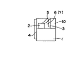
図1はこの発明の第1実施形態の半導体レーザ装置の要部の斜視図であり、図2は図1のII−II線から見た断面図である。
【0018】
図1,図2において、1はコーナー部に切り欠き1aを有する略直方体形状の放熱台、2は上記放熱台1の切り欠き1aの壁面の上側に固定された半導体レーザとしてのLD、3は上記LD2の後端面からの光出力をモニタするためのモニタ用受光素子としてのモニタ用PD、4は上記放熱台1の上面に固定された信号受光用受光素子としての信号受光用PDである。上記放熱台1の切り欠き1aの下側部分に金属製の矩形のブロック10をエポキシ樹脂等により固定し、そのブロック10上にモニタ用PD3を固定している。こうすると、LD2の後端面とモニタ用PD3との間隔を1mm程度まで狭くすることができる。このLD2の後端面とモニタ用PD3との間隔は、狭い方が後述する遮光性樹脂で覆いやすいが、あまり狭くすると、LD2の搭載位置精度を高くしなければならないので、0.1mm〜2mm程度とし、望ましくは0.5mm〜1.5mm程度がよい。
【0019】
生産上、LD2の後端面とモニタ用PD3との間隔があまり狭いと、LD2の後端面がモニタ用PD3に当たってしまう可能性が高くなるので、2mm程度まで広げておいた方が、早く生産することが可能となる。
【0020】
上記LD2の後端面とモニタ用PD3との間を覆う遮光性樹脂からなる遮光部5を形成する。この遮光性樹脂は室温で液状のものを用い、シリンジによりLD2の後端面とモニタ用PD3との間に滴下する。上記LD2の後端面とモニタ用PD3との間隔が十分狭ければ遮光性樹脂を滴下しても隙間に入らないので、遮光性樹脂に囲まれた空間6が形成される。
【0021】
この遮光性樹脂は、UV硬化性(または熱硬化性)で、粘度はLD2の後端面とモニタ用PD3の隙間に入らない程度の粘性の高いものを選ぶ。その後、UV光を照射(または加熱)して硬化させる。なお、遮光性樹脂としては、LD2の波長780nmの出射光が透過しないものなら何でも良く、例えばホトカプラの外装用に使用されているような熱硬化性を有する黒色エポキシ樹脂を使用してもよい。
【0022】
また、上記ブロック10としては、レーザ光の出射方向の長さがLD2の後端面とモニタ用PD3との間隔が1mm〜2mm程度になるものを使用する。また、モニタ用PD3の受光面とレーザ光の光軸とのなす角度は、戻り光による影響が少なくなるように垂直より少し傾けた方がよい。また、上記モニタ用PD3の中心がLD2のレーザ光の光軸に近くなるようにブロック10の搭載部分を切り欠いてもよい。
【0023】
上記構成の半導体レーザ装置において、LD2の後端面から出射した光のうちモニタ用PD3で受光されなかったものは、遮光性樹脂で散乱,吸収されるため、信号受光用PD4に入射することがなく、従って光ディスク信号の受信を妨害することがない。したがって、簡単な構成で迷光の発生を防止でき、迷光に起因するノイズを低減することができる。
【0024】
また、上記LD2の後端面にモニタ用PD3が近いので、従来のモニタ用PDより小さいモニタ用PDを使用しても十分な信号出力が得られる。
【0025】
上記第1実施形態では、LD2,信号受光用PD4が固定されている放熱台1(金属,セラミック等の放熱が良いもので作製する)にモニタ用PD3が固定されているブロック10を固定したが、放熱台とブロックを一体成形してもよい。
【0026】
(第2実施形態)
また、この発明の第2実施形態の半導体レーザ装置は、樹脂部分を除いて図1,図2に示す半導体レーザ装置と同一の構成をしており、同一構成部は説明を省略し、図1,図2を援用する。
【0027】
図2に示すように、LD2の後端面とモニタ用PD3との間に透光性樹脂を充填し、UV照射または熱硬化により流れないようにして透光性樹脂部7を形成した後、その透光性樹脂部7を遮光性樹脂で覆う(樹脂の滴下を2回行う)。上記LD2の出射光に対して透光性を有する樹脂をLD2とモニタ用PD3との間に滴下して透光性樹脂部7を形成することによって、LD2の後端面からモニタ用PD3までの光路を確保した上で、透光性樹脂部7を覆うように遮光性樹脂からなる遮光部5を形成する。
【0028】
この透光性樹脂としては、UV硬化樹脂,エポキシ樹脂等のLD2の波長780nmの出射光が透過するものなら何でもよく、例えば弾力性のあるシリコンゴム系の樹脂がよい。ただし、透光性樹脂は、粘性が低くてLD2の後端面とモニタ用PD3との間に入りやすく、かつ、表面張力が高くてLD2の後端面とモニタ用PD3との間からはみ出さないものが最もよい。
【0029】
上記構成の半導体レーザ装置において、LD2の後端面から出射されたレーザ光は、従来の半導体レーザ装置の場合と同様、モニタ用PD3表面で一部が反射されるが、遮光性樹脂5に遮られて、キャップ25内の空間にまで放出されることはないので、迷光の発生を防止することができる。
【0030】
また、光路を埋める透光性樹脂部7によって、LD2の後端面とモニタ用PD3との間に遮光性樹脂が入り込むことがないので、光路を囲む遮光性樹脂からなる遮光部5を確実に作成することができる。
【0031】
また、上記LD2の後端面とモニタ用PD3との間隔は従来に比べて狭くしているので、そのLD2とモニタ用PD3との間の空間に透光性樹脂を滴下しても、透光性樹脂の表面張力により支えられて、周囲に広がることがない。その結果、少ない量の透光性樹脂で済ますことができると共に、不要な部分に透光性樹脂が付着するのを防止することができる。上記LD2の後端面とモニタ用PD3との間隔としては2mm以下が望ましく、1mm以下がより好ましい。また、LD2の後端面をモニタ用PD3の受光面の凹凸から0.1mm以上離しておく必要がある。
【0032】
【発明の効果】
以上より明らかなように、この発明の半導体レーザ装置によれば、半導体レーザと、上記半導体レーザの後端面からの光出力をモニターするためのモニタ用受光素子と、上記半導体レーザの前端面からの光出力の反射光を受光する信号受光用受光素子とを有する半導体レーザ装置において、上記半導体レーザの後端面とモニタ用受光素子との間の光路外に光が出ないように上記光路を覆う樹脂からなる遮光部を設けたものであり、上記半導体レーザとモニタ用受光素子との間隔を0.1mm以上2mm以下とし、遮光性樹脂の粘性と間隔により、遮光性樹脂で覆われた空間が光路に形成されたものである。
【0033】
したがって、上記半導体レーザ装置によれば、半導体レーザの後端面から出射した光のうちモニタ用受光素子で受光されなかったものは、樹脂からなる遮光部で遮るため、上記半導体レーザの前端面からの光出力の反射光を受光する信号受光用受光素子に入射することがないので、簡単な構成で迷光の発生を防止でき、迷光に起因するノイズを低減することができる。
【0034】
【0035】
【0036】
また、上記モニタ用受光素子を放熱台に設けられたブロックに搭載したので、モニタ用受光素子を放熱台が固定されるアイレットの平面よりも離れた位置に配置でき、モニタ用受光素子のワイヤボンディング時にアイレットが邪魔にならないようにできる。
【図面の簡単な説明】
【図1】 図1はこの発明の第1実施形態の半導体レーザ装置の半導体レーザ装置の要部の斜視図である。
【図2】 図2は図1のII−II線から見た断面図である。
【図3】 図3は従来の半導体レーザ装置の半導体レーザ装置の全体を示す斜視図である。
【図4】 図4は上記半導体レーザ装置の要部の斜視図である。
【図5】 図5は図4のV−V線から見た断面図である。
【符号の説明】
1…放熱台、
2…LD、
3…モニタ用PD、
4…信号受光用PD、
5…遮光部
6…空間、
7…透光性樹脂部、
10…ブロック。[0001]
BACKGROUND OF THE INVENTION
The present invention relates to a semiconductor laser device used for an optical disk pickup or the like.
[0002]
[Prior art]
A conventional semiconductor laser device is shown in FIG. As shown in FIG. 3, this semiconductor laser device includes a laser diode (hereinafter referred to as LD) 22 that is a light source for signal reading, and a monitor photodiode (hereinafter referred to as PD) that monitors the intensity of laser light emitted from the
[0003]
[Problems to be solved by the invention]
FIG. 4 shows a state in which the
[0004]
FIG. 5 is a cross-sectional view taken along line VV in FIG. 4. The LD 22 is mounted on the
[0005]
SUMMARY OF THE INVENTION An object of the present invention is to provide a semiconductor laser device that can prevent the generation of stray light and reduce noise with a simple configuration.
[0006]
[Means for Solving the Problems]
In order to achieve the above object, a semiconductor laser device according to the present invention includes a semiconductor laser, a light receiving element for monitoring light output from the rear end face of the semiconductor laser, and light output from the front end face of the semiconductor laser. In a semiconductor laser device having a signal receiving light receiving element for receiving the reflected light, a light shielding property that covers the optical path so that light does not go out of the optical path between the rear end surface of the semiconductor laser and the monitoring light receiving element A light-shielding portion made of resin is provided, and the interval between the semiconductor laser and the light-receiving element for monitoring is 0.1 mm or more and 2 mm or less. It is formed in the optical path.
[0007]
According to the semiconductor laser device having the above configuration, light emitted from the rear end face of the semiconductor laser that is not received by the monitor light receiving element is blocked by the light shielding portion made of resin. Therefore, the light output of the semiconductor laser does not interfere with the reception of the reflected light reflected by the optical disk or the like. Therefore, generation of stray light can be prevented with a simple configuration, and noise caused by stray light can be reduced.
[0008]
[0009]
[0010]
[0011]
[0012]
[0013]
[0014]
A semiconductor laser device according to an embodiment is characterized in that the light-receiving element for monitoring is mounted on a block provided on a heat radiating table.
[0015]
According to the semiconductor laser device of the above embodiment, by mounting the monitor light receiving element on a block provided on the heat radiating stand, the monitor light receiving element is placed at a position away from the plane of the eyelet to which the heat radiating base is fixed. It is possible to dispose the eyelet so that it does not get in the way during wire bonding of the monitor light receiving element.
[0016]
DETAILED DESCRIPTION OF THE INVENTION
The semiconductor laser device of the present invention will be described in detail below with reference to the illustrated embodiments.
[0017]
(First embodiment)
FIG. 1 is a perspective view of an essential part of the semiconductor laser device according to the first embodiment of the present invention, and FIG. 2 is a sectional view taken along line II-II in FIG.
[0018]
1 and 2,
[0019]
In production, if the distance between the rear end surface of the
[0020]
A
[0021]
As this light-shielding resin, a UV-curable (or thermosetting) resin having a viscosity that does not enter the gap between the rear end face of the
[0022]
Further, as the
[0023]
In the semiconductor laser device having the above configuration, light emitted from the rear end face of the
[0024]
Further, since the
[0025]
In the first embodiment, the
[0026]
(Second Embodiment)
The semiconductor laser device according to the second embodiment of the present invention has the same configuration as that of the semiconductor laser device shown in FIGS. 1 and 2 except for the resin portion, and the description of the same components is omitted. FIG. 2 is incorporated.
[0027]
As shown in FIG. 2, after filling the light-transmitting resin between the rear end surface of the
[0028]
The translucent resin may be anything such as UV curable resin, epoxy resin, or the like that can transmit the emitted light having a wavelength of 780 nm of LD2, and for example, an elastic silicone rubber resin. However, the translucent resin is low in viscosity and easily enters between the rear end surface of the
[0029]
In the semiconductor laser device having the above configuration, the laser light emitted from the rear end surface of the
[0030]
Further, since the light-shielding resin does not enter between the rear end face of the
[0031]
Further, since the distance between the rear end face of the
[0032]
【The invention's effect】
As apparent from the above, according to the semiconductor laser device of the present invention, the semiconductor laser, the monitoring light receiving element for monitoring the light output from the rear end face of the semiconductor laser, and the front end face of the semiconductor laser are provided. In a semiconductor laser device having a light receiving element for receiving light that receives reflected light of light output, a resin that covers the optical path so that light does not go out of the optical path between the rear end face of the semiconductor laser and the light receiving element for monitoring der which the light shielding portion is provided consisting of is, the distance between the semiconductor laser and the monitor light-receiving element and 0.1mm above 2mm or less, the viscosity and spacing of the light-shielding resin, is covered with a light-shielding resin space It is formed in the optical path .
[0033]
Therefore, according to the semiconductor laser device, light emitted from the rear end face of the semiconductor laser that is not received by the light receiving element for monitoring is shielded by the light shielding portion made of resin. Since it does not enter the light receiving element for receiving signal light that receives the reflected light of the light output, stray light can be prevented from being generated with a simple configuration, and noise caused by stray light can be reduced.
[0034]
[0035]
[0036]
In addition, since the monitor light receiving element is mounted on a block provided on the heat radiating stand, the monitor light receiving element can be arranged at a position away from the plane of the eyelet to which the heat radiating base is fixed, and wire bonding of the monitor light receiving element is possible. Sometimes you can keep your eyelets out of the way.
[Brief description of the drawings]
FIG. 1 is a perspective view of an essential part of a semiconductor laser device of a semiconductor laser device according to a first embodiment of the present invention.
FIG. 2 is a sectional view taken along line II-II in FIG.
FIG. 3 is a perspective view showing an entire semiconductor laser device of a conventional semiconductor laser device.
FIG. 4 is a perspective view of a main part of the semiconductor laser device.
FIG. 5 is a cross-sectional view taken along line VV of FIG.
[Explanation of symbols]
1 ... Heat sink,
2 ... LD,
3 ... PD for monitoring,
4 ... PD for signal reception,
5 ... Shading
7: Translucent resin part,
10 ... Block.
Claims (2)
上記半導体レーザの後端面と上記モニタ用受光素子との間の光路外に光が出ないように上記光路を覆う遮光性樹脂からなる遮光部を設け、
上記半導体レーザと上記モニタ用受光素子との間隔を0.1mm以上2mm以下とし、
上記遮光性樹脂の粘性と上記間隔により、上記遮光性樹脂で覆われた空間が上記光路に形成されたことを特徴とする半導体レーザ装置。Semiconductor having a semiconductor laser, a light receiving element for monitoring for monitoring the light output from the rear end face of the semiconductor laser, and a light receiving element for signal receiving for receiving reflected light of the light output from the front end face of the semiconductor laser In the laser device,
Providing a light-shielding portion made of a light-shielding resin that covers the optical path so that no light is emitted outside the optical path between the rear end face of the semiconductor laser and the light-receiving element for monitoring;
The interval between the semiconductor laser and the light receiving element for monitoring is 0.1 mm or more and 2 mm or less,
A semiconductor laser device characterized in that a space covered with the light-shielding resin is formed in the optical path by the viscosity of the light-shielding resin and the interval.
上記モニタ用受光素子を放熱台に設けられたブロックに搭載したことを特徴とする半導体レーザ装置。The semiconductor laser device according to claim 1 ,
A semiconductor laser device, wherein the light-receiving element for monitoring is mounted on a block provided on a heat sink.
Priority Applications (1)
| Application Number | Priority Date | Filing Date | Title |
|---|---|---|---|
| JP2000140051A JP3766780B2 (en) | 2000-05-12 | 2000-05-12 | Semiconductor laser device |
Applications Claiming Priority (1)
| Application Number | Priority Date | Filing Date | Title |
|---|---|---|---|
| JP2000140051A JP3766780B2 (en) | 2000-05-12 | 2000-05-12 | Semiconductor laser device |
Publications (2)
| Publication Number | Publication Date |
|---|---|
| JP2001326409A JP2001326409A (en) | 2001-11-22 |
| JP3766780B2 true JP3766780B2 (en) | 2006-04-19 |
Family
ID=18647404
Family Applications (1)
| Application Number | Title | Priority Date | Filing Date |
|---|---|---|---|
| JP2000140051A Expired - Fee Related JP3766780B2 (en) | 2000-05-12 | 2000-05-12 | Semiconductor laser device |
Country Status (1)
| Country | Link |
|---|---|
| JP (1) | JP3766780B2 (en) |
Families Citing this family (1)
| Publication number | Priority date | Publication date | Assignee | Title |
|---|---|---|---|---|
| JP4982469B2 (en) | 2008-10-31 | 2012-07-25 | 株式会社日立製作所 | Optical module |
-
2000
- 2000-05-12 JP JP2000140051A patent/JP3766780B2/en not_active Expired - Fee Related
Also Published As
| Publication number | Publication date |
|---|---|
| JP2001326409A (en) | 2001-11-22 |
Similar Documents
| Publication | Publication Date | Title |
|---|---|---|
| JP5765619B2 (en) | Light emitting device | |
| JP2007281472A (en) | Semiconductor radiation source and photocuring device | |
| JP5345358B2 (en) | Casing with lower casing | |
| JP2013175773A (en) | Optical sensor and method of optically detecting object | |
| US11226402B2 (en) | Optical ranging systems including optical cross-talk reducing features | |
| JP3233837B2 (en) | Semiconductor laser device and optical pickup device | |
| JP3835608B2 (en) | Laser equipment | |
| US20050151216A1 (en) | Integrated circuit device packaging structure and packaging method | |
| JP2005234464A (en) | Optical transceiver and optical module used therefor | |
| JP3766780B2 (en) | Semiconductor laser device | |
| CN110090359B (en) | Skin or hair treatment device and method for manufacturing same | |
| JP2014011107A (en) | Led light source device and exposure device including the same | |
| TWI611231B (en) | Optical assembly position adjustment device | |
| JPS6316682A (en) | Resin-sealed light emitting module | |
| JPH1041539A (en) | Structure of inflared ray transmitting/receiving module | |
| CN219246680U (en) | Photoelectric chip packaging structure and reflective photoelectric encoder | |
| CN211829532U (en) | Laser module | |
| JP2542746B2 (en) | Laser diode | |
| JPH07170024A (en) | Semiconductor device | |
| WO2024062910A1 (en) | Light-emitting device, light source unit, and vehicle | |
| JP7183821B2 (en) | Light source device and distance measuring device | |
| KR100731859B1 (en) | Laser diode having structure for improving noise-characteristics of optical external feedback | |
| JP3318083B2 (en) | Semiconductor laser device | |
| JP2000058962A (en) | Semiconductor laser device | |
| JP3660305B2 (en) | Manufacturing method of semiconductor laser device |
Legal Events
| Date | Code | Title | Description |
|---|---|---|---|
| A977 | Report on retrieval |
Free format text: JAPANESE INTERMEDIATE CODE: A971007 Effective date: 20040906 |
|
| A131 | Notification of reasons for refusal |
Free format text: JAPANESE INTERMEDIATE CODE: A131 Effective date: 20050419 |
|
| A521 | Written amendment |
Free format text: JAPANESE INTERMEDIATE CODE: A523 Effective date: 20050614 |
|
| A02 | Decision of refusal |
Free format text: JAPANESE INTERMEDIATE CODE: A02 Effective date: 20051011 |
|
| A521 | Written amendment |
Free format text: JAPANESE INTERMEDIATE CODE: A523 Effective date: 20051125 |
|
| A911 | Transfer to examiner for re-examination before appeal (zenchi) |
Free format text: JAPANESE INTERMEDIATE CODE: A911 Effective date: 20051221 |
|
| TRDD | Decision of grant or rejection written | ||
| A01 | Written decision to grant a patent or to grant a registration (utility model) |
Free format text: JAPANESE INTERMEDIATE CODE: A01 Effective date: 20060124 |
|
| A61 | First payment of annual fees (during grant procedure) |
Free format text: JAPANESE INTERMEDIATE CODE: A61 Effective date: 20060130 |
|
| R150 | Certificate of patent or registration of utility model |
Free format text: JAPANESE INTERMEDIATE CODE: R150 |
|
| FPAY | Renewal fee payment (event date is renewal date of database) |
Free format text: PAYMENT UNTIL: 20100203 Year of fee payment: 4 |
|
| LAPS | Cancellation because of no payment of annual fees |