JP3760552B2 - Inrush current limiting method - Google Patents
Inrush current limiting method Download PDFInfo
- Publication number
- JP3760552B2 JP3760552B2 JP07749197A JP7749197A JP3760552B2 JP 3760552 B2 JP3760552 B2 JP 3760552B2 JP 07749197 A JP07749197 A JP 07749197A JP 7749197 A JP7749197 A JP 7749197A JP 3760552 B2 JP3760552 B2 JP 3760552B2
- Authority
- JP
- Japan
- Prior art keywords
- time
- inrush current
- current limiting
- smoothing capacitor
- power failure
- Prior art date
- Legal status (The legal status is an assumption and is not a legal conclusion. Google has not performed a legal analysis and makes no representation as to the accuracy of the status listed.)
- Expired - Fee Related
Links
Images


Landscapes
- Emergency Protection Circuit Devices (AREA)
- Stand-By Power Supply Arrangements (AREA)
- Direct Current Feeding And Distribution (AREA)
- Rectifiers (AREA)
Description
【0001】
【発明の属する技術分野】
本発明はコンバータ回路における交流電源停電後の復電時に対する突入電流制限方法に関する。
【0002】
【従来の技術】
図4はこの種の突入電流制限方法の従来例を用いるコンバータ回路の構成を示す回路図である。
コンバータ回路のダイオードブリッジ1は交流電源より入力し、整流して負荷5に直流電流を供給する。突入電流制限抵抗3は負荷5と直列に、また、平滑コンデンサ4は負荷5と並列に、それぞれ設けられている。そこで、リレーコイル21 と接点22 とよりなるリレーは、負荷の通電中は突入電流制限抵抗3を接点22 で短絡し、交流電源の停電を検出したときは接点22 を開いて突入電流制限抵抗3を負荷回路に投入することにより、復電時における突入電流を制限していた。
【0003】
【発明が解決しようとする課題】
上述した従来例の場合では、交流電源が停電してから突入電流制限抵抗3が投入されるまでのリレーの動作時間に一定の遅延時間があるので、この間に平滑コンデンサ4の端子電圧が低下する。したがって瞬間停電のため接点21 がオフするまでの間に復電した場合には、過大な突入電流が流れてダイオードブリッジ1のパワー素子やリレー接点等を損傷するという欠点があった。
そこで、本発明は、交流電源が瞬間停電しても復電時の突入電流を常に小さい値に抑制して回路素子の保護を行う突入電流制限方法を提供することを目的とする。
【0004】
【課題を解決するための手段】
本発明では、交流電源の停電時における平滑コンデンサの端子間電圧降下値を、復電時の突入電流が過大とならないような値に予め定めておく。そこで、停電の都度、停電時から平滑コンデンサの端子間電圧がこの所定電圧降下値だけ低下するまでの時間を演算し、算出した時間が経過する以前に突入電流制限抵抗を投入することとしている。
【0005】
【発明の実施の形態】
次に、本発明の実施の形態を図面を参照して説明する。
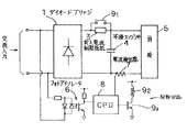
図1は本発明の突入電流制限方法の一形態例を用いたコンバータ回路を示す回路図である。
図4の従来例と異なる点は、交流電源の停電を検出するリレーの代りに交流側電圧の半周期ごとに電圧の有無を検出するフォトアイソレータ6と、直流側の負荷電流を検出する電流検出器7と、突入電流制限抵抗3の短絡用接点91 用のコイル92 とトランジスタ93 とを含む駆動回路と、フォトアイソレータ6および電流検出器7からの入力と所定の平滑コンデンサ電圧降下値ならびに交流電源の停電検出の動作遅れとを考慮して駆動回路を動作させる時間を演算するCPU8とより構成されていることである。
【0006】
次に、本形態例による動作を図2のフローチャートを用いて説明する。
CPU8は起動とともに常時、交流電源の電圧の有無をフォトアイソレータ6を介して監視し(ステップS1)、フォトアイソレータ6から電源遮断の通報を受けると次式により突入電流制限抵抗3を投入すべき時間tを演算する(ステップS2)。
t=C(V−Vs )/i−1/2f ・・・・(1)
但し、C:平滑コンデンサ4の容量
V:通電時の平滑コンデンサ4の端子間電圧
Vs :復電時に過大な突入電流を生じない平滑コンデンサ4の残留端子電圧の所定値
i:交流電源の停電による平滑コンデンサ4の放電開始時の負荷電流
f:交流電源周波数
次に、CPU8は停電検出時から時間tが経過したか否かを調べ(ステップS3)、時間tが経過した時点で駆動回路を動作させて接点91 をオフとし、突入電流抵抗を投入して(ステップS4)動作を終了する。
【0007】
式(1)の第1項は、停電後の復電時に平滑コンデンサ4の端子間の電圧降下が、過大な突入電流を生じないような許容範囲内に入っている限度の経過時間を算出するものである。また、式(1)の第2項は、停電検出時の動作遅れ時間を考慮して、安全側に時間tを演算するためのものである。
【0008】
【発明の効果】
以上説明したように本発明は、交流電源の停止の都度、平滑コンデンサから負荷への放電電流の値その他を用いて適切な突入電流制限抵抗の投入時間を演算して、停電後のこの時間の経過する時点で突入電流制限抵抗を投入することにより、特に極めて短時間の停電の場合でも遅れることなく、突入電流が過大となることを防いで回路素子の破損を防ぐことができるという効果がある。
【図面の簡単な説明】
【図1】本発明の突入電流制限方法の1実施形態例を適用したコンバータ回路の構成図である。
【図2】図1のコンバータ回路の停電時の動作を説明するフローチャートである。
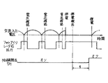
【図3】図1のフォトアイソレータ6による交流電圧検出とフォトアイソレータ6および短絡用接点91のタイミングチャートである。
【図4】コンバータ回路の突入電流制限方法の従来例を適用した回路構成図である。
【符号の説明】
1 ダイオードブリッジ
21 ,91 接点
22 ,92 コイル
3 突入電流制限抵抗
4 平滑コンデンサ
5 負荷
6 フォトアイソレータ
7 電流検出器
8 CPU[0001]
BACKGROUND OF THE INVENTION
The present invention relates to an inrush current limiting method for a power recovery after an AC power failure in a converter circuit.
[0002]
[Prior art]
FIG. 4 is a circuit diagram showing a configuration of a converter circuit using a conventional example of this type of inrush current limiting method.
The diode bridge 1 of the converter circuit is input from an AC power source and rectified to supply a DC current to the
[0003]
[Problems to be solved by the invention]
In the case of the above-described conventional example, the relay operating time from when the AC power supply is interrupted to when the inrush current limiting
Therefore, an object of the present invention is to provide an inrush current limiting method for protecting circuit elements by always suppressing an inrush current at the time of power recovery to a small value even when an AC power supply is instantaneously interrupted.
[0004]
[Means for Solving the Problems]
In the present invention, the voltage drop value between the terminals of the smoothing capacitor at the time of a power failure of the AC power supply is determined in advance so that the inrush current at the time of power recovery does not become excessive. Therefore, every time a power failure occurs, the time from the time of the power failure until the voltage across the terminals of the smoothing capacitor decreases by this predetermined voltage drop value is calculated, and the inrush current limiting resistor is inserted before the calculated time elapses.
[0005]
DETAILED DESCRIPTION OF THE INVENTION
Next, embodiments of the present invention will be described with reference to the drawings.
FIG. 1 is a circuit diagram showing a converter circuit using an embodiment of the inrush current limiting method of the present invention.
4 differs from the conventional example of FIG. 4 in that a photo isolator 6 that detects the presence or absence of a voltage every half cycle of the AC side voltage, and a current detection that detects a load current on the DC side, instead of a relay that detects a power failure of the AC power supply. , A drive circuit including a coil 9 2 for a short-circuit contact 9 1 of the inrush current limiting
[0006]
Next, the operation according to this embodiment will be described with reference to the flowchart of FIG.
The
t = C (V−V s ) / i−1 / 2f (1)
However, C: capacitance of the smoothing capacitor 4 V: terminal voltage V s of energization when the smoothing capacitor 4: predetermined value i of the residual terminal voltage of the
[0007]
The first term of the formula (1) calculates the elapsed time of the limit that the voltage drop between the terminals of the
[0008]
【The invention's effect】
As described above, the present invention calculates the appropriate inrush current limiting resistor input time using the value of the discharge current from the smoothing capacitor to the load, etc., every time the AC power supply is stopped. By injecting the inrush current limiting resistor at the time when it has elapsed, there is an effect that it is possible to prevent the inrush current from becoming excessive and prevent damage to the circuit element without delay even in the case of a power failure for a very short time. .
[Brief description of the drawings]
FIG. 1 is a configuration diagram of a converter circuit to which an embodiment of an inrush current limiting method of the present invention is applied.
FIG. 2 is a flowchart for explaining the operation of the converter circuit of FIG. 1 during a power failure.
3 is a AC voltage detector and photo isolator 6 and a timing chart of the short-circuiting contact 9 1 by the photo isolator 6 of FIG.
FIG. 4 is a circuit configuration diagram to which a conventional example of a converter circuit inrush current limiting method is applied.
[Explanation of symbols]
1 Diode Bridge 2 1 , 9 1
Claims (2)
交流電源の停電時における直流側平滑コンデンサの端子間電圧降下値を、予め所定値に定めておき、
停電の都度、停電時から平滑コンデンサの電圧降下が前記所定値に到達するまでの時間を演算し、
交流電源が停電してから前記時間の経過するまでに前記突入電流制限抵抗を投入することを特徴とする突入電流制限方法。In a converter circuit that performs DC conversion by inputting from an AC power supply, an inrush current limiting method for suppressing an inrush current by inserting an inrush current limiting resistor in series with a load when the power is turned on,
The voltage drop value between the terminals of the DC side smoothing capacitor at the time of a power failure of the AC power supply is set to a predetermined value in advance,
Every time a power failure occurs, calculate the time from the time of the power failure until the voltage drop of the smoothing capacitor reaches the predetermined value,
The inrush current limiting method is characterized in that the inrush current limiting resistor is inserted between the time when the AC power supply fails and the time elapses.
Priority Applications (1)
| Application Number | Priority Date | Filing Date | Title |
|---|---|---|---|
| JP07749197A JP3760552B2 (en) | 1997-03-28 | 1997-03-28 | Inrush current limiting method |
Applications Claiming Priority (1)
| Application Number | Priority Date | Filing Date | Title |
|---|---|---|---|
| JP07749197A JP3760552B2 (en) | 1997-03-28 | 1997-03-28 | Inrush current limiting method |
Publications (2)
| Publication Number | Publication Date |
|---|---|
| JPH10271668A JPH10271668A (en) | 1998-10-09 |
| JP3760552B2 true JP3760552B2 (en) | 2006-03-29 |
Family
ID=13635468
Family Applications (1)
| Application Number | Title | Priority Date | Filing Date |
|---|---|---|---|
| JP07749197A Expired - Fee Related JP3760552B2 (en) | 1997-03-28 | 1997-03-28 | Inrush current limiting method |
Country Status (1)
| Country | Link |
|---|---|
| JP (1) | JP3760552B2 (en) |
Families Citing this family (9)
| Publication number | Priority date | Publication date | Assignee | Title |
|---|---|---|---|---|
| JP2001112265A (en) | 1999-10-06 | 2001-04-20 | Hitachi Ltd | Inverter device and motor drive device |
| JP4609868B2 (en) * | 1999-12-17 | 2011-01-12 | 河村電器産業株式会社 | Control method of AC voltage regulator |
| JP5279796B2 (en) | 2010-10-29 | 2013-09-04 | 三菱電機株式会社 | Power converter |
| JP5817565B2 (en) * | 2012-02-02 | 2015-11-18 | 富士通株式会社 | Power distribution device, power distribution system, and inrush current suppression method |
| JP5460838B2 (en) * | 2012-12-10 | 2014-04-02 | 三菱電機株式会社 | Power converter |
| GB2515587B (en) * | 2013-11-26 | 2017-08-09 | Keymed (Medical & Ind Equipment) Ltd | Inrush current limiter |
| JP6930336B2 (en) | 2017-09-27 | 2021-09-01 | ヤマハ株式会社 | Power supply circuit and audio equipment |
| CN108199572B (en) * | 2017-12-25 | 2021-03-30 | 苏州英威腾电力电子有限公司 | Frequency converter and power-off protection system thereof |
| CN120847530B (en) * | 2025-09-22 | 2025-12-30 | 深圳长虹聚和源科技有限公司 | Method and system for detecting energy storage power supply load access state |
-
1997
- 1997-03-28 JP JP07749197A patent/JP3760552B2/en not_active Expired - Fee Related
Also Published As
| Publication number | Publication date |
|---|---|
| JPH10271668A (en) | 1998-10-09 |
Similar Documents
| Publication | Publication Date | Title |
|---|---|---|
| KR960012527B1 (en) | Inverter device provided with charge and discharge control circuit of DC smoothing capacitor and manufacturing method thereof | |
| JP3760552B2 (en) | Inrush current limiting method | |
| KR20170064890A (en) | Arcless DC Circuit Breaker using Semiconductor Switch | |
| JP2007174792A (en) | Grid-connected inverter device | |
| KR20180110586A (en) | Power supply apparatus with soft―start and protection | |
| JPH02231922A (en) | Inrush current prevention system for motor driver upon recovery from instantaneous power interruption | |
| JPH06245485A (en) | Inverter device | |
| JP3565054B2 (en) | Inverter device protection method | |
| JP3369890B2 (en) | Inverter abnormality detection circuit | |
| JP3543692B2 (en) | Ozone generator | |
| JP5259941B2 (en) | Inverter device and air conditioner | |
| JP7524680B2 (en) | Power Conversion Equipment | |
| JP2010074928A (en) | Inverter device | |
| JP2000201484A (en) | Inverter device | |
| JP2815230B2 (en) | Discharge lamp lighting device | |
| JPH11341820A (en) | Voltage-type inverter | |
| JP3775251B2 (en) | Multi-output power supply circuit and multi-output power supply method | |
| JP2004215457A (en) | Power supply circuit | |
| CN112311240B (en) | Switching power supply device | |
| JP3048502B2 (en) | Inrush current prevention circuit | |
| JPH0537632Y2 (en) | ||
| CN110291691A (en) | Circuit for inrush current limiting at power supply | |
| JPH03245772A (en) | Charge protective circuit for capacitor | |
| JP2006294539A (en) | Relay control device | |
| JP2003174778A (en) | Relay non-operation detecting circuit and motor control device including the same |
Legal Events
| Date | Code | Title | Description |
|---|---|---|---|
| A621 | Written request for application examination |
Free format text: JAPANESE INTERMEDIATE CODE: A621 Effective date: 20040109 |
|
| A977 | Report on retrieval |
Free format text: JAPANESE INTERMEDIATE CODE: A971007 Effective date: 20051213 |
|
| TRDD | Decision of grant or rejection written | ||
| A01 | Written decision to grant a patent or to grant a registration (utility model) |
Free format text: JAPANESE INTERMEDIATE CODE: A01 Effective date: 20051220 |
|
| A61 | First payment of annual fees (during grant procedure) |
Free format text: JAPANESE INTERMEDIATE CODE: A61 Effective date: 20060102 |
|
| R150 | Certificate of patent (=grant) or registration of utility model |
Free format text: JAPANESE INTERMEDIATE CODE: R150 |
|
| FPAY | Renewal fee payment (prs date is renewal date of database) |
Free format text: PAYMENT UNTIL: 20100120 Year of fee payment: 4 |
|
| FPAY | Renewal fee payment (prs date is renewal date of database) |
Free format text: PAYMENT UNTIL: 20110120 Year of fee payment: 5 |
|
| FPAY | Renewal fee payment (prs date is renewal date of database) |
Free format text: PAYMENT UNTIL: 20110120 Year of fee payment: 5 |
|
| FPAY | Renewal fee payment (prs date is renewal date of database) |
Free format text: PAYMENT UNTIL: 20120120 Year of fee payment: 6 |
|
| LAPS | Cancellation because of no payment of annual fees |