JP3758397B2 - High frequency transmitter / receiver and in-vehicle radar system - Google Patents
High frequency transmitter / receiver and in-vehicle radar system Download PDFInfo
- Publication number
- JP3758397B2 JP3758397B2 JP00494999A JP494999A JP3758397B2 JP 3758397 B2 JP3758397 B2 JP 3758397B2 JP 00494999 A JP00494999 A JP 00494999A JP 494999 A JP494999 A JP 494999A JP 3758397 B2 JP3758397 B2 JP 3758397B2
- Authority
- JP
- Japan
- Prior art keywords
- transmission
- connection terminal
- base plate
- reception circuit
- circuit
- Prior art date
- Legal status (The legal status is an assumption and is not a legal conclusion. Google has not performed a legal analysis and makes no representation as to the accuracy of the status listed.)
- Expired - Fee Related
Links
Images


Classifications
-
- H—ELECTRICITY
- H10—SEMICONDUCTOR DEVICES; ELECTRIC SOLID-STATE DEVICES NOT OTHERWISE PROVIDED FOR
- H10W—GENERIC PACKAGES, INTERCONNECTIONS, CONNECTORS OR OTHER CONSTRUCTIONAL DETAILS OF DEVICES COVERED BY CLASS H10
- H10W90/00—Package configurations
- H10W90/701—Package configurations characterised by the relative positions of pads or connectors relative to package parts
- H10W90/751—Package configurations characterised by the relative positions of pads or connectors relative to package parts of bond wires
- H10W90/754—Package configurations characterised by the relative positions of pads or connectors relative to package parts of bond wires between a chip and a stacked insulating package substrate, interposer or RDL
Landscapes
- Variable-Direction Aerials And Aerial Arrays (AREA)
- Waveguide Aerials (AREA)
- Support Of Aerials (AREA)
- Radar Systems Or Details Thereof (AREA)
Description
【0001】
【発明の属する技術分野】
本発明は、自動車用レーダや無線LAN等に用いられる高周波送受信装置及び車載レーダシステムに関する。
【0002】
【従来の技術】
自動車用レーダや無線LAN等に用いられる高周波送受信装置では搭載性や可搬性の観点から装置の小型、簡素化が重要な要素と成っている。
【0003】
従来の自動車用レーダに用いられる送受信装置の一例として、1997年電子情報通信学会総合大会C−2−121「60GHz帯ミリ波レーダユニット」(従来文献1)がある。この従来技術では、ミリ波(60GHz帯)送受信回路を匡体内に入れた送受信ユニットを単独に作っておき、これに別個に作ったアンテナユニットを接続する。送受信ユニットの裏面及びアンテナユニットにはRF信号の入出力端となる導波管端子を設けられており、両者は導波管により接続される。
【0004】
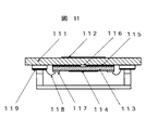
また、特開平8−250913号(従来文献2)には、MMIC(モノリシックマイクロ波集積回路)を密閉収容するパッケージの外面に平面アンテナを形成する例が開示されている。図11にその構造を示す。パッケージの底面111の外側にアンテナ112が、アンテナ112と対向してパッケージの内側にMMIC113が取り付けられている。MMIC113の底面にはアース導体層115の一部分が取り除かれたスロット116が設けられている。スロット116を介して、MMIC113の表面に設けた高周波回路を構成する導体114とアンテナ112とが電磁的に結合する。MMIC113の表面に設けられたボンディングパッド117とパッケージ外からの電源供給用の電源端子119とはボンディングワイヤ118により接続されている。
【0005】
【発明が解決しようとする課題】
従来文献1の例では、それぞれ単独に設計された送受信ユニットとアンテナユニットとを接続することにより高周波送受信装置を構成する。この構造は、送受信ユニットとアンテナユニットの特性を別々に評価出来る利点が有るものの、部品点数が増えると共に構造が複雑となり、装置の小型、簡素化を図るには不適である。特に、ミリ波帯のような超高周波帯で導波管により接続する場合には、機械加工面での複雑さを増し、コスト高となる等の課題があった。
【0006】
従来文献2の例では、高周波回路とアンテナとをスロットにより電磁的に結合させている。このような非接触構造による結合では、高周波信号に対する挿入損失が大きくなる傾向がある。挿入損失を小さくするためには、アンテナと高周波回路との間にある導体板111の厚さを出来るだけ薄くする必要がある。例えば、10GHz信号についての設計例で0.5〜0.7mm程度との報告例があり、ミリ波帯(約60GHz)信号では一層薄くする必要がある。そのため、アンテナと高周波回路を導体板の両面に設ける構成では、機械的強度を維持することが難しく、実現するためには何らかの補強のための機構が必要になると考えられる。さらに、ミリ波のような短波長の信号を電磁的に結合するためにはスロットの寸法精度やアンテナパタン112と高周波回路パタン114との位置関係の精度を極めて高くする必要があり、組立作業が難しくなる。MMICの信頼性を向上させるためにはパッケージ全体を気密構造とする必要があり、このことは組立作業を一層複雑にする。
【0007】
【課題を解決するための手段】
本発明は、ベースプレートと、ベースプレートの第一の面上に設けられたアンテナと、ベースプレートの第一の面と相対する第二の面上に設けられ、アンテナと電気的に接続された送受信回路と、ベースプレートの第二の面上に設けられ、送受信回路に電源電流を供給するもしくは信号を出力する外部端子とを備え、ベースプレートは、第一の面側にアンテナにより覆われた凹部と、凹部と第二の面を貫通する孔とを有しており、送受信回路に電源電流を供給するもしくは信号を出力する接続端子は、孔を通って凹部において外部端子と接続されており、接続端子は孔においてベースプレートと電気的に絶縁された芯線を持つ線路構造とすることを特徴とする。
【0008】
さらに、送受信回路とアンテナを接続する同軸線路を用いることで、電源やIF信号の入出力端子の同軸線路が同じ構造でかつ同じ方向となり、組立時の作業性が向上するとともに部品の共通化が図れ、半導体チップを含む送受信回路部を容易に気密構造とすることができるようになる。
【0009】
【発明の実施の形態】
現在、交通事故や渋滞等の道路交通システムの問題を解決することを目的として、新たな道路交通システムの研究開発が進められている。その一つとして、自動車にレーダを搭載し、前方車との距離を測ったり、道路上の障害物を検知して、運転制御を行う車載レーダシステムが検討されている。その構成を図12に示す。
【0010】
アンテナユニット121は、ミリ波を送信し、送信したミリ波が前方車または障害物から反射して戻ってくる反射波を受信し、送信周波数と反射波の周波数との差を検出する。ミリ波は、従来の赤外線レーザに比較して気象条件に影響されにくく、距離を精度よく検出することができるものである。
【0011】
検出されたミリ波の周波数と反射波の周波数との差から、前方車との相対速度が求められる。また、位相差等から車間距離、自車からみた前方車の位置する方向を検出することができる。信号処理ユニット122は、アンテナユニット121の出力から、このような演算処理を行い、周囲の状況を判断し、自動車に対して必要な制御を行う。例えば、スロットル制御、トランスミッション制御、ブレーキ制御である。一方、自動車を自動制御するばかりでなく、ドライバにも周囲の状況(障害物の存在、前方車の存在、その相対速度等)を知らせ、あるいは場合によっては警報を発する必要がある。信号処理ユニット122は、ドライバディスプレイ123に対して、これらの情報を送る。ドライバディスプレイ123は、信号処理ユニット122から送信された信号に応じて、表示処理、警報を報知する。
【0012】
なお、図12においては信号処理ユニットとアンテナユニットとを別々に設けているが、アンテナユニットを小型化することによって、一つのユニットとすることができる。このように信号処理ユニットとアンテナユニットを一体化すると、自動車への実装が簡易化できる。
【0013】
このように、アンテナユニットは自動車の前面(側面)に取り付けられるため、小型・軽量化することが必要である。その一方で、自動車の走行時の振動等の影響を受けることから、高い機械的強度を維持する必要がある。
【0014】
図1は本発明の実施の形態であるアンテナユニットに使用される高周波送受信装置の断面図である。金属性のベースプレート1の上面にアンテナを構成する誘電体から成るアンテナ基板2を、下面に送受信回路を構成する誘電体から成る回路基板3と半導体チップ(MMIC)4を接着する。回路基板3の表面に設けられた回路パタン導体10とアンテナ基板2の表面に設けられたアンテナパタン導体7とは誘電体6−1と金属性の芯線6−2からなるRF用同軸線路により接続されている。MMICはパッケージされていないため、送受信回路は金属で作られた送受信回路カバー5により気密封止されている。回路パタン導体10及び半導体チップ4とはボンディングワイヤにより接続されている。なお、半導体チップ4は回路基板3上に直接接続される、いわゆるフリップチップ実装された構造でもよい。また、ベースプレート1と送受信回路カバー5は、プラスチック等の非金属で形成し、その表面を金属のメッキや蒸着等により覆ったものでも良い。
【0015】
ベースプレート1は送受信回路が設けられている周縁部1−1と中央部1−2とを分割可能な構造となっている。中央部1−2には少なくとも送受信回路カバー5により気密封止される部分が含まれるように分割する。このようにベースプレート1を分割構造とすることにより、送受信回路の面積がアンテナの面積に比べ十分小さな場合に、全体の組立時の作業性を良くすることができる。
【0016】
ベースプレートの中央部1−2に、電源供給用端子やIF信号用端子として端子用芯線8−1と端子用誘電体8−2から成る同軸構造の接続端子(同軸状端子)がアンテナ面と略垂直になるように設けられる。ベースプレートの中央部1−2は、図3に示すようにアンテナ基板が接着される側の一部がくり貫かれている。このように形成されたベースプレートの凹部において端子用芯線8−1は外部端子を形成するリード線9と接続され、リード線9により外部の電源回路や信号処理回路に接続される。なお、送受信回路とアンテナとを接続する同軸線路は、高周波送受信装置が送信用アンテナと受信用アンテナの2つを備えている場合にはそれぞれについて送受信回路と接続するために2つの同軸状端子が必要となる。また、電源供給用端子やIF信号用端子も図に示した筐体の片側のみならず、筐体の両側に設けてもよく、端子の数も特に限定されない。
【0017】
図2は高周波送受信装置の裏面から見た図である。点線は表面に接着されたアンテナ基板2を示す。
【0018】
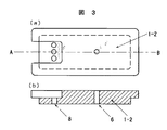
図3に本発明のベースプレートの中央部1−2の構造を示す。図3(a)が、中央部1−2の上面図、図3(b)が、中央部1−2の図3(a)におけるA−Bとして示した位置での断面図である。6は送受信回路とアンテナとを接続する同軸線路用の孔であり、8は電源供給用もしくはIF信号用の同軸状端子の孔である。上述したように、アンテナ基板が接着される側の一部がくり貫かれ、同軸状端子からの信号線が通される。
【0019】
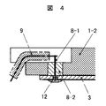
図4は同軸状端子の部分を拡大した断面図である。ベースプレート中央部1―2の下面に送受信回路を構成する誘電体基板3が貼り付けられる。誘電体基板3に孔を空け、同軸状端子の芯線8−1の一端をその孔に差し込み、半田12で送受信回路パタン導体に接続する。芯線8−1の他端は、絶縁物で被覆されたリード線(外部端子)9に接続されている。リード線9は外部の信号処理回路に接続されている。このリード線は端子の数が多い場合には市販されているフラットケーブル等が活用できる。同軸状端子の芯線8−1を支える誘電体8−2は電気的に絶縁されておればよい。誘電体8−2としてセラミックやガラスを使用することで、送受信回路を気密性を高め、送受信回路の信頼性を向上させることができる。
【0020】
芯線8−1と送受信回路パタン導体との接続において、誘電体基板3の孔の側面をメッキ等の導体層で覆う。これにより、金属導体とハンダとは接続性がよいため、誘電体基板と中心導体の間にハンダを隙間無く充填することができ、機械的強度が増す。
【0021】
図5は、同軸状端子の別の構成例である。芯線8−1の一端を長くしておき、その芯線8−1が外部の信号処理回路へ接続するためのリード線を兼ね、他端はボンディングワイヤにより送受信回路パタン導体と接続する。さらに、図5の例では、同軸状端子としてコバール、鉄等の金属スリーブ13を用いた同軸状端子を別途作成しておき溶接、半田付け等でベースプレート中央部1−2と接続するようにしている。
【0022】
図6は、高周波送受信装置の別の構成例であり、アンテナの面積があまり大きくない場合、あるいはアンテナ基板が厚い等の理由によりアンテナ基板だけで必要な強度を保持できる場合に有効な構成例である。ベースプレートを周縁部1−1と中央部1−2に分割せず、中央部1−2に相当するベースプレートの上に直接アンテナ基板2を取り付ける。
【0023】
図7は、送信用アンテナと受信用アンテナとを別々に設けた場合の構成例であり、その場合に電源供給用端子とIF用端子を左右両端に設けた場合であり、アンテナ導体と回路導体を接続する高周波(RF)同軸線路6−1、6−2が左右2個所に設けてある。
【0024】
図8は、本発明の高周波送受信装置において送受共用アンテナを用いた場合の実施例を示し、図8(a)は高周波(RF)回路構成例を、図8(b)は誘電体基板3上に設けられるRF回路パタンを示す。図8(a)において、発振器27からのRF信号はサーキュレータ22を経てアンテナ21から送信される。アンテナ21は送受共用となっており受信RF信号はサーキュレータ22を経てミクサ23に加えられる。一方発振器27からのRF信号の一部は結合器25を経て局発信号としてミクサ23に加えられ、受信RF信号はIF信号に変換される。変換されたIF信号はIF信号端子24から取り出される。
【0025】
図8(b)において、半導体チップで作られた発振器27からのRF信号はマイクロストリップ線路28を通りサーキュレータ22を経てRF回路とアンテナとを接続するRF同軸端子30に加えられる。各半導体チップには電源供給用端子31より誘電体基板3の上に設けられた電源供給用線路29(図では点線で示した)により直流電源が供給される。
【0026】
ここで、図8(b)に示すように、電源供給用端子31とIF信号端子24とは誘電体基板3の相対する辺の付近に設け、IF信号線と電源供給線とが並列しないようにすることが望ましい。IF信号線と電源供給線とが並列すると、電源に含まれる雑音によってIF信号に雑音を受ける可能性があるためである。回路配置上、IF信号線と電源供給線とが並列する場合には、両者の間にグランド線(アース)を設け、電源供給線からの雑音がIF信号線に流入することを防止することができる。
【0027】
図9は、送信アンテナと受信アンテナを別個に設けた場合の実施例を示し、図9(a)はRF回路構成例を、図9(b)はそのRF回路パタンを示す。図9(a)において、発信器27からのRF信号は分配器34を経て、RF増幅器33を通って送信アンテナ21−1から送信される。受信アンテナ21−2で受信された受信RF信号はミクサ23に加えられ、一方、発信器27からのRF信号の一部が分配器34を経て局発信号としてミクサ23に加えられる。図9(b)において、半導体チップで作られた発信器27からのRF信号はマイクロストリップ線路28を通りRF回路と送信アンテナとを接続するRF同軸端子30―1に加えられ、受信アンテナからの受信信号はRF同軸端子30―2より半導体チップで作られたミクサ23に加えられる。
【0028】
図10は、送信アンテナと受信アンテナを別個に設け、かつさらに前方の車両や障害物の方向を正確に捉えるため、受信アンテナを複数設けた場合の実施例を示し、図10(a)はRF回路構成例を、図10(b)はそのRF回路パタンを示す。図10(a)において、発信器27からのRF信号は分配器34―1を経て、RF増幅器33を通って送信アンテナ21−1から送信される。また、複数の受信アンテナ21−2、21−3で受信されたRF信号はミクサ23−1、23−2に加えられ、一方、発信器27からのRF信号の一部が分配器34−1、34−2を経て局発信号としてミクサ23−1、23−2に加えられる。図10(b)において、半導体チップで作られた発信器27からのRF信号はマイクロストリップ線路28を通りRF回路と送信アンテナとを接続するRF同軸端子30−1に加えられ、受信アンテナからの受信信号はRF同軸端子30−2、30−3より半導体チップで作られたミクサ23−1、23−2に加えられる。
【0029】
図9(b)、図10(b)に示す実施例でも、IF信号端子24と電源供給端子31とを誘電体基板3の相対する辺に設け、IF信号線と電源供給線とが平行に並ぶのを防止している。
【0030】
【発明の効果】
本発明によれば、外部端子と送受信回路とを接続する接続端子に同軸状端子を使用することにより、送受信回路の気密性を保持しつつ、高周波送受信回路組立時の作業性を向上させることができる。
【図面の簡単な説明】
【図1】本発明の高周波送受信装置の断面図である。
【図2】本発明の高周波送受信装置の裏面の上面図である。
【図3】本発明の高周波送受信装置のベースプレート中央部を示す図である。
【図4】本発明の高周波送受信装置のIF信号端子(同軸状端子)の一構成例を拡大した断面図である。
【図5】本発明の高周波送受信装置のIF信号端子(同軸状端子)の別の構成例を拡大した断面図である。
【図6】本発明の高周波送受信装置の断面図である。
【図7】本発明の高周波送受信装置の断面図である。
【図8】(a)は高周波回路の構成例を、(b)はその回路パタンを示す図である。
【図9】(a)は高周波回路の構成例を、(b)はその回路パタンを示す図である。
【図10】(a)は高周波回路の構成例を、(b)はそのRF回路パタンを示す図である。
【図11】従来の高周波送受信装置の断面図である。
【図12】車載レーダシステムを示す図である。
【符号の説明】
1…ベースプレート、2…アンテナ基板、3…回路基板、4…半導体チップ、5…送受信回路カバー、6…RF同軸線路、7…アンテナパタン導体、8…IF同軸線路、9…リード線、10…送受信回路パタン導体、11…ボンディングワイヤ、12…ハンダ、13…金属スリーブ、21…アンテナ、22…サーキュレータ、23…ミクサ、24…IF出力端子、25…結合器、26…抵抗、27…発振器、28…マイクロストリップ線路、29…電源線路、30…同軸線路端子、31…電源端子、32…誘電体基板、33…RF増幅器、34…分配器。[0001]
BACKGROUND OF THE INVENTION
The present invention relates to a high-frequency transmission / reception device and an in-vehicle radar system used for automotive radar, wireless LAN, and the like.
[0002]
[Prior art]
In high-frequency transmission / reception devices used for automobile radars, wireless LANs, and the like, miniaturization and simplification of the devices are important factors from the viewpoint of mountability and portability.
[0003]
As an example of a transmission / reception device used in a conventional automotive radar, there is the 1997 IEICE General Conference C-2-121 “60 GHz-band millimeter-wave radar unit” (conventional document 1). In this prior art, a transmission / reception unit in which a millimeter wave (60 GHz band) transmission / reception circuit is placed in a housing is made independently, and an antenna unit made separately is connected thereto. The back surface of the transmission / reception unit and the antenna unit are provided with waveguide terminals serving as input / output ends of RF signals, and both are connected by a waveguide.
[0004]
Japanese Patent Laid-Open No. 8-250913 (conventional document 2) discloses an example in which a planar antenna is formed on the outer surface of a package for hermetically housing an MMIC (monolithic microwave integrated circuit). FIG. 11 shows the structure. An antenna 112 is attached to the outside of the bottom surface 111 of the package, and an MMIC 113 is attached to the inside of the package so as to face the antenna 112. A
[0005]
[Problems to be solved by the invention]
In the example of
[0006]
In the example of
[0007]
[Means for Solving the Problems]
The present invention includes a base plate, an antenna provided on the first surface of the base plate, a transmission / reception circuit provided on the second surface opposite to the first surface of the base plate, and electrically connected to the antenna. An external terminal provided on the second surface of the base plate, for supplying a power supply current to the transmission / reception circuit or outputting a signal, the base plate having a concave portion covered with an antenna on the first surface side, and a concave portion And a connection terminal for supplying a power supply current to the transmission / reception circuit or outputting a signal is connected to the external terminal in the recess through the hole, and the connection terminal is a hole. A line structure having a core wire electrically insulated from the base plate is provided.
[0008]
Furthermore, by using a coaxial line that connects the transceiver circuit and antenna, the coaxial lines of the power supply and IF signal input / output terminals have the same structure and the same direction, improving the workability during assembly and making parts common As a result, the transmission / reception circuit portion including the semiconductor chip can be easily formed into an airtight structure.
[0009]
DETAILED DESCRIPTION OF THE INVENTION
Currently, research and development of new road traffic systems are underway for the purpose of solving problems of road traffic systems such as traffic accidents and traffic jams. As one of them, an on-vehicle radar system that controls operation by mounting a radar on an automobile and measuring a distance from a preceding vehicle or detecting an obstacle on a road has been studied. The configuration is shown in FIG.
[0010]
The antenna unit 121 transmits a millimeter wave, receives a reflected wave that the transmitted millimeter wave is reflected from a preceding vehicle or an obstacle and returns, and detects a difference between the transmission frequency and the frequency of the reflected wave. Millimeter waves are less susceptible to weather conditions than conventional infrared lasers, and can detect distances with high accuracy.
[0011]
From the difference between the detected frequency of the millimeter wave and the frequency of the reflected wave, the relative speed with the preceding vehicle is obtained. Further, it is possible to detect the inter-vehicle distance from the phase difference or the like and the direction in which the vehicle ahead is viewed from the own vehicle. The signal processing unit 122 performs such arithmetic processing from the output of the antenna unit 121, determines the surrounding situation, and performs necessary control on the automobile. For example, throttle control, transmission control, and brake control. On the other hand, it is necessary not only to automatically control the automobile, but also to inform the driver of the surrounding conditions (the presence of obstacles, the presence of a forward vehicle, the relative speed thereof, etc.), or in some cases to issue an alarm. The signal processing unit 122 sends these pieces of information to the
[0012]
In FIG. 12, the signal processing unit and the antenna unit are provided separately. However, by reducing the size of the antenna unit, it can be made one unit. When the signal processing unit and the antenna unit are integrated as described above, mounting on an automobile can be simplified.
[0013]
Thus, since the antenna unit is attached to the front (side) of the automobile, it is necessary to reduce the size and weight. On the other hand, it is necessary to maintain a high mechanical strength because it is affected by vibrations and the like during driving of the automobile.
[0014]
FIG. 1 is a cross-sectional view of a high frequency transmitting / receiving apparatus used in an antenna unit according to an embodiment of the present invention. An
[0015]
The
[0016]
In the central portion 1-2 of the base plate, a connection terminal (coaxial terminal) having a coaxial structure composed of a terminal core wire 8-1 and a terminal dielectric 8-2 as a power supply terminal and an IF signal terminal is substantially the same as the antenna surface. It is provided to be vertical. As shown in FIG. 3, a part of the base plate 1-2 on the side to which the antenna substrate is bonded is cut out. The terminal core wire 8-1 is connected to the
[0017]
FIG. 2 is a diagram seen from the back side of the high-frequency transmitting / receiving device. The dotted line shows the
[0018]
FIG. 3 shows the structure of the central portion 1-2 of the base plate of the present invention. 3A is a top view of the central portion 1-2, and FIG. 3B is a cross-sectional view of the central portion 1-2 at the position indicated by AB in FIG. 3A. 6 is a hole for a coaxial line connecting the transmission / reception circuit and the antenna, and 8 is a hole for a coaxial terminal for power supply or IF signal. As described above, a part of the side to which the antenna substrate is bonded is cut out, and the signal line from the coaxial terminal is passed.
[0019]
FIG. 4 is an enlarged cross-sectional view of the coaxial terminal portion. A
[0020]
In connection between the core wire 8-1 and the transmission / reception circuit pattern conductor, the side surface of the hole of the
[0021]
FIG. 5 shows another configuration example of the coaxial terminal. One end of the core wire 8-1 is lengthened, the core wire 8-1 also serves as a lead wire for connection to an external signal processing circuit, and the other end is connected to a transmission / reception circuit pattern conductor by a bonding wire. Further, in the example of FIG. 5, a coaxial terminal using a
[0022]
FIG. 6 shows another configuration example of the high-frequency transmitter / receiver, which is effective when the area of the antenna is not so large, or when the required strength can be maintained only by the antenna substrate because the antenna substrate is thick. is there. The
[0023]
FIG. 7 shows a configuration example in which a transmitting antenna and a receiving antenna are provided separately. In this case, a power supply terminal and an IF terminal are provided at both left and right ends. Are provided at two places on the left and right sides.
[0024]
FIG. 8 shows an embodiment in which a transmission / reception shared antenna is used in the high-frequency transmitting / receiving apparatus of the present invention, FIG. 8 (a) is a configuration example of a high-frequency (RF) circuit, and FIG. The RF circuit pattern provided in FIG. In FIG. 8A, the RF signal from the
[0025]
In FIG. 8B, an RF signal from an
[0026]
Here, as shown in FIG. 8B, the
[0027]
FIG. 9 shows an embodiment in which a transmitting antenna and a receiving antenna are provided separately, FIG. 9A shows an example of an RF circuit configuration, and FIG. 9B shows an RF circuit pattern thereof. In FIG. 9A, the RF signal from the
[0028]
FIG. 10 shows an embodiment in which a transmitting antenna and a receiving antenna are provided separately, and a plurality of receiving antennas are provided in order to accurately capture the direction of a vehicle or an obstacle ahead. FIG. FIG. 10 (b) shows an example of the circuit configuration and its RF circuit pattern. In FIG. 10A, the RF signal from the
[0029]
9B and 10B, the
[0030]
【The invention's effect】
According to the present invention, by using a coaxial terminal as a connection terminal for connecting an external terminal and a transmission / reception circuit, workability at the time of assembling a high-frequency transmission / reception circuit can be improved while maintaining airtightness of the transmission / reception circuit. it can.
[Brief description of the drawings]
FIG. 1 is a cross-sectional view of a high-frequency transmitting / receiving apparatus of the present invention.
FIG. 2 is a top view of the back surface of the high-frequency transmitting / receiving device of the present invention.
FIG. 3 is a diagram showing a central portion of a base plate of a high frequency transmitting / receiving apparatus of the present invention.
FIG. 4 is an enlarged cross-sectional view of a configuration example of an IF signal terminal (coaxial terminal) of the high-frequency transmitting / receiving device of the present invention.
FIG. 5 is an enlarged cross-sectional view of another configuration example of the IF signal terminal (coaxial terminal) of the high-frequency transceiver device of the present invention.
FIG. 6 is a cross-sectional view of the high-frequency transmitting / receiving apparatus of the present invention.
FIG. 7 is a cross-sectional view of the high-frequency transmitting / receiving device of the present invention.
8A is a diagram illustrating a configuration example of a high-frequency circuit, and FIG. 8B is a diagram illustrating a circuit pattern thereof.
9A is a diagram illustrating a configuration example of a high-frequency circuit, and FIG. 9B is a diagram illustrating a circuit pattern thereof.
10A is a diagram showing a configuration example of a high-frequency circuit, and FIG. 10B is a diagram showing an RF circuit pattern thereof.
FIG. 11 is a cross-sectional view of a conventional high-frequency transmitting / receiving device.
FIG. 12 is a diagram showing an in-vehicle radar system.
[Explanation of symbols]
DESCRIPTION OF
Claims (10)
上記ベースプレートの第1の面上に設けられたアンテナと、
上記ベースプレートの上記第1の面と相対する第2の面上に設けられ、上記アンテナと電気的に接続された送受信回路と、
上記ベースプレートに設けられ、上記送受信回路に電源電流を供給するもしくは信号を入出力する外部端子と接続される接続端子とを備え、
上記ベースプレートは上記アンテナと上記送受信回路とを接続する伝送線路を有し、
上記ベースプレートは、上記第1の面に開口部を有する凹部を有すると共に、上記凹部の底面と上記第2の面とを貫通する孔を有し、
上記接続端子は、上記孔にて上記ベースプレートと電気的に絶縁された芯線を持つ線路構造を有し、
上記接続端子の上記芯線の一端は上記高周波送受信回路と接続され、
上記接続端子の上記芯線の他端は、上記凹部内にて上記外部端子と接続され、
上記接続端子は、上記芯線を上記ベースプレートから絶縁するためのガラス又はセラミックを含む誘電体を用いた気密構造を有する
ことを特徴とする高周波送受信装置。A conductive base plate;
An antenna provided on the first surface of the base plate;
A transmission / reception circuit provided on a second surface opposite to the first surface of the base plate and electrically connected to the antenna;
A connection terminal provided on the base plate and connected to an external terminal for supplying a power supply current to the transmission / reception circuit or inputting / outputting a signal;
The base plate has a transmission line connecting the antenna and the transmission / reception circuit,
The base plate has a recess having an opening on the first surface and a hole penetrating the bottom surface of the recess and the second surface.
The connection terminal has a line structure having a core wire electrically insulated from the base plate in the hole,
One end of the core wire of the connection terminal is connected to the high-frequency transmission / reception circuit,
The other end of the core wire of the connection terminal is connected to the external terminal in the recess ,
The high-frequency transmission / reception device , wherein the connection terminal has an airtight structure using a dielectric material including glass or ceramic for insulating the core wire from the base plate .
上記アンテナと上記送受信回路とを接続する上記伝送線路は上記ベースプレートを貫通する同軸線路であることを特徴とする高周波送受信装置。In claim 1,
The high-frequency transmission / reception apparatus, wherein the transmission line connecting the antenna and the transmission / reception circuit is a coaxial line penetrating the base plate.
上記接続端子又は上記同軸線路は、金属製の円筒状スリーブを外導体としてその内側に絶縁体と芯線とが設けられた線路構造を有すること特徴とする高周波送受信装置。In claim 2 ,
The high-frequency transmitting / receiving apparatus according to claim 1, wherein the connection terminal or the coaxial line has a line structure in which a metal cylindrical sleeve is used as an outer conductor and an insulator and a core wire are provided on the inner side.
上記接続端子であって、上記送受信回路に電源電流を供給する第1の接続端子と、
上記接続端子であって、上記送受信回路へ信号を入出力する第2の接続端子とを有し、
上記第1の接続端子と上記第2の接続端子とは、それぞれ上記送受信回路の形成された送受信回路基板の相異なる辺側に設けられていることを特徴とする高周波送受信装置。In claim 1,
A first connection terminal for supplying a power source current to the transmission / reception circuit;
A second connection terminal for inputting / outputting a signal to / from the transmission / reception circuit;
The high-frequency transmission / reception apparatus, wherein the first connection terminal and the second connection terminal are provided on different sides of the transmission / reception circuit board on which the transmission / reception circuit is formed.
上記接続端子であって、上記送受信回路に電源電流を供給する第1の接続端子と、
上記接続端子であって、上記送受信回路へ信号を入出力する第2の接続端子と、
上記第1の接続端子と上記送受信回路とを接続する第1の線路と、
上記第2の接続端子と上記送受信回路とを接続する第2の線路とを有し、
上記第1の線路と上記第2の線路とは、上記送受信回路の形成される回路基板上で、並列に延伸しないことを特徴とする高周波送受信装置。In claim 1,
A first connection terminal for supplying a power source current to the transmission / reception circuit;
A second connection terminal for inputting / outputting a signal to / from the transmission / reception circuit;
A first line connecting the first connection terminal and the transmission / reception circuit;
A second line connecting the second connection terminal and the transmission / reception circuit;
The high-frequency transmission / reception apparatus, wherein the first line and the second line do not extend in parallel on a circuit board on which the transmission / reception circuit is formed.
上記接続端子であって、上記送受信回路に電源電流を供給する第1の接続端子と、
上記接続端子であって、上記送受信回路へ信号を入出力する第2の接続端子と、
上記第1の接続端子と上記送受信回路とを接続する第1の線路と、
上記第2の接続端子と上記送受信回路とを接続する第2の線路とを有し、
上記第1の線路と上記第2の線路とは、上記送受信回路の形成される回路基板上で、並列に延伸し、
上記第1の線路と上記第2の線路との間にグランド線が設けられていることを特徴とする高周波送受信装置。In claim 1,
A first connection terminal for supplying a power source current to the transmission / reception circuit;
A second connection terminal for inputting / outputting a signal to / from the transmission / reception circuit;
A first line connecting the first connection terminal and the transmission / reception circuit;
A second line connecting the second connection terminal and the transmission / reception circuit;
The first line and the second line extend in parallel on a circuit board on which the transmission / reception circuit is formed,
A high-frequency transmitting / receiving device, wherein a ground line is provided between the first line and the second line.
上記高周波送受信回路と上記アンテナとは、上記ベースプレートの上記第1の面と上記第2の面との間の部分を貫通するRF用同軸線路により接続され、
上記ベースプレートは上記第1の面に相対する第3の面を更に有し、上記第1の面と上記第3の面との距離は上記第1の面と上記第2の面との距離より短く、
上記ベースプレートの上記第1の面と上記第3の面との間の部分を貫通するように配置されると共にガラス又はセラミックを含む誘電体を介して上記ベースプレートから電気的に絶縁された芯線を持つ気密線路構造を具備する接続端子を有し、
上記接続端子の上記芯線の一端は上記高周波送受信回路と接続され、
上記接続端子の上記芯線の他端は上記ベースプレートの上記第3の面側に設けられると共に電源回路及び信号処理回路を含む外部回路と接続されている
ことを特徴とする高周波送受信装置。A high-frequency transmission / reception circuit including an oscillator, an amplifier, and a mixer circuit; and an antenna for transmitting / receiving a high-frequency signal, wherein the high-frequency transmission / reception circuit and the antenna are connected to a first surface of a single conductive base plate. A high-frequency transmitting / receiving device having an integrated circuit-antenna structure provided on each of the second surfaces facing the first surface,
The high-frequency transmitting / receiving circuit and the antenna are connected by an RF coaxial line that penetrates a portion between the first surface and the second surface of the base plate,
The base plate further includes a third surface facing the first surface, and a distance between the first surface and the third surface is greater than a distance between the first surface and the second surface. Short ,
Having an electrically insulated core wire from the base plate through the dielectric including the placed Rutotomoni glass or ceramic so as to penetrate the portion between the first surface and the third surface of the base plate Having a connection terminal with an airtight line structure,
One end of the core wire of the connection terminal is connected to the high-frequency transmission / reception circuit,
RF transceiver other end of the core wire of the connecting terminals, characterized in <br/> that is connected to an external circuit including a power supply circuit and a signal processing circuit with provided to the third surface side of the base plate .
コバール、鉄等の金属製の円筒状スリーブを外導体とし、上記円筒状スリーブ内部に絶縁物と芯線とが設けられた個別部品を、上記RF用同軸線路または上記接続端子として用い、
上記個別部品は溶接を含む工程により上記ベースプレートに取り付けられている
ことを特徴とする高周波送受信装置。In claim 7 ,
Using a cylindrical sleeve made of metal such as Kovar or iron as an outer conductor, an individual part provided with an insulator and a core wire inside the cylindrical sleeve is used as the RF coaxial line or the connection terminal,
The high frequency transmitting / receiving apparatus according to claim 1, wherein the individual parts are attached to the base plate by a process including welding.
上記接続端子の上記芯線の他端が、上記外部回路に直接接続するリード線を兼ねるよう延伸していることを特徴とする高周波送受信装置。In claim 7 ,
RF transmitting and receiving apparatus other end of the core wire of the connecting terminals, characterized in that it extends to serve as the leads that connect directly to the external circuit.
上記外部回路と上記接続端子の上記芯線の他端とを接続するリード線は、絶縁被覆で覆われたフラットケーブルで構成されると共に、上記ベースプレートの上記第3の面に沿った方向に上記リード線が出るように溶接を含む工程により取り付けられていることを特徴とする高周波送受信装置。In claim 7 ,
The external circuit and the lead wire for connecting the other end of the core wire of the connecting terminal, as well as composed of a flat cable covered with an insulating coating, said lead in a direction along the third surface of the base plate A high-frequency transmission / reception apparatus, wherein the high-frequency transmission / reception apparatus is attached by a process including welding so that a wire comes out.
Priority Applications (3)
| Application Number | Priority Date | Filing Date | Title |
|---|---|---|---|
| JP00494999A JP3758397B2 (en) | 1999-01-12 | 1999-01-12 | High frequency transmitter / receiver and in-vehicle radar system |
| EP99306230A EP0978729A3 (en) | 1998-08-07 | 1999-08-05 | High-frequency transmitter-receiving apparatus for such an application as vehicle-onboard radar system |
| US09/369,400 US6249242B1 (en) | 1998-08-07 | 1999-08-06 | High-frequency transmitter-receiver apparatus for such an application as vehicle-onboard radar system |
Applications Claiming Priority (1)
| Application Number | Priority Date | Filing Date | Title |
|---|---|---|---|
| JP00494999A JP3758397B2 (en) | 1999-01-12 | 1999-01-12 | High frequency transmitter / receiver and in-vehicle radar system |
Publications (2)
| Publication Number | Publication Date |
|---|---|
| JP2000209026A JP2000209026A (en) | 2000-07-28 |
| JP3758397B2 true JP3758397B2 (en) | 2006-03-22 |
Family
ID=11597835
Family Applications (1)
| Application Number | Title | Priority Date | Filing Date |
|---|---|---|---|
| JP00494999A Expired - Fee Related JP3758397B2 (en) | 1998-08-07 | 1999-01-12 | High frequency transmitter / receiver and in-vehicle radar system |
Country Status (1)
| Country | Link |
|---|---|
| JP (1) | JP3758397B2 (en) |
Families Citing this family (12)
| Publication number | Priority date | Publication date | Assignee | Title |
|---|---|---|---|---|
| JP3801884B2 (en) * | 2001-07-23 | 2006-07-26 | 株式会社日立製作所 | High frequency transmitter / receiver |
| JP4523223B2 (en) | 2002-04-26 | 2010-08-11 | 株式会社日立製作所 | Radar sensor |
| JP3786939B2 (en) * | 2003-09-10 | 2006-06-21 | 大阪瓦斯株式会社 | Exploration equipment |
| KR100737098B1 (en) * | 2006-03-16 | 2007-07-06 | 엘지이노텍 주식회사 | Electromagnetic shielding device and manufacturing process |
| JP2008283676A (en) * | 2007-04-10 | 2008-11-20 | Toto Ltd | High frequency sensor apparatus |
| JP2009058450A (en) * | 2007-08-31 | 2009-03-19 | Fujitsu Ten Ltd | Unit chassis of radar device |
| KR101426584B1 (en) | 2011-12-09 | 2014-08-06 | 주식회사 만도 | Radar apparatus and method of manufacturing the same |
| JP6348396B2 (en) * | 2014-10-07 | 2018-06-27 | 株式会社Soken | Antenna device |
| WO2018037655A1 (en) * | 2016-08-24 | 2018-03-01 | 株式会社村田製作所 | Antenna module |
| JP2022175694A (en) * | 2021-05-14 | 2022-11-25 | 国立大学法人東京工業大学 | phased array antenna |
| JP2023098311A (en) | 2021-12-28 | 2023-07-10 | 本田技研工業株式会社 | Structure to attach object detection device to vehicle body |
| JP2023098310A (en) * | 2021-12-28 | 2023-07-10 | 本田技研工業株式会社 | Mounting structure of the object detection device to the vehicle body |
Family Cites Families (10)
| Publication number | Priority date | Publication date | Assignee | Title |
|---|---|---|---|---|
| JPS5326934Y2 (en) * | 1973-12-29 | 1978-07-08 | ||
| JPH03117926U (en) * | 1990-03-16 | 1991-12-05 | ||
| JP2606521Y2 (en) * | 1992-02-27 | 2000-11-27 | 株式会社村田製作所 | Antenna device |
| JPH0637401A (en) * | 1992-07-20 | 1994-02-10 | Nec Corp | Optical semiconductor container |
| JPH06112719A (en) * | 1992-09-28 | 1994-04-22 | Nec Corp | Electronic scanning antenna |
| JPH08204444A (en) * | 1995-01-31 | 1996-08-09 | Mitsumi Electric Co Ltd | GPS antenna with integrated converter function |
| JPH0983202A (en) * | 1995-09-13 | 1997-03-28 | Fukushima Nippon Denki Kk | Microwave waveguide |
| JPH09150691A (en) * | 1995-11-30 | 1997-06-10 | Fujitsu Ten Ltd | Warning device and car to car distance control device |
| JP3266491B2 (en) * | 1996-02-29 | 2002-03-18 | 京セラ株式会社 | High frequency package |
| JP3718939B2 (en) * | 1997-01-14 | 2005-11-24 | 松下電工株式会社 | Discharge lamp lighting device |
-
1999
- 1999-01-12 JP JP00494999A patent/JP3758397B2/en not_active Expired - Fee Related
Also Published As
| Publication number | Publication date |
|---|---|
| JP2000209026A (en) | 2000-07-28 |
Similar Documents
| Publication | Publication Date | Title |
|---|---|---|
| US6249242B1 (en) | High-frequency transmitter-receiver apparatus for such an application as vehicle-onboard radar system | |
| JP4523223B2 (en) | Radar sensor | |
| JP4861303B2 (en) | Radar sensor | |
| JP5209610B2 (en) | High frequency circuit board, high frequency circuit module, and radar apparatus | |
| US7436679B2 (en) | Radio-frequency module for communication | |
| JP5707657B2 (en) | Small microwave components for surface mounting | |
| JP3758397B2 (en) | High frequency transmitter / receiver and in-vehicle radar system | |
| JP3801884B2 (en) | High frequency transmitter / receiver | |
| JP2006507740A (en) | Package electronic components for applications at millimeter frequencies | |
| JP2010256327A (en) | Dual-band antenna array and RF front end for millimeter-wave imagers and radar | |
| WO2006049877A2 (en) | Tapered slot feed for an automotive radar ant | |
| JPH08250913A (en) | MMIC package assembly | |
| JP4588073B2 (en) | Small electronic components for microwave applications | |
| US20080316126A1 (en) | Antenna System for a Radar Transceiver | |
| JP2000059140A (en) | High frequency transceiver | |
| JP5179570B2 (en) | High frequency module, method for manufacturing the same, transmitter, receiver, transmitter / receiver, and radar apparatus including the high frequency module | |
| JPH10261917A (en) | Millimeter wave transceiver | |
| JP2002084208A (en) | High frequency module and high frequency wireless device | |
| JP2981067B2 (en) | FM signal generator and high-frequency signal generator of FM radar module | |
| JP4745943B2 (en) | Electronic circuit, transmitter, receiver, transceiver | |
| JP2003008314A (en) | High frequency module | |
| JP2981068B2 (en) | FM signal generator and high-frequency signal generator of FM radar module | |
| JP2011003651A (en) | Circuit device and electronic apparatus | |
| JP2922741B2 (en) | Radar module | |
| JPH0697735A (en) | High frequency signal generator |
Legal Events
| Date | Code | Title | Description |
|---|---|---|---|
| A977 | Report on retrieval |
Free format text: JAPANESE INTERMEDIATE CODE: A971007 Effective date: 20050325 |
|
| A131 | Notification of reasons for refusal |
Free format text: JAPANESE INTERMEDIATE CODE: A131 Effective date: 20050329 |
|
| A521 | Request for written amendment filed |
Free format text: JAPANESE INTERMEDIATE CODE: A523 Effective date: 20050530 |
|
| A131 | Notification of reasons for refusal |
Free format text: JAPANESE INTERMEDIATE CODE: A131 Effective date: 20050920 |
|
| A521 | Request for written amendment filed |
Free format text: JAPANESE INTERMEDIATE CODE: A523 Effective date: 20051118 |
|
| TRDD | Decision of grant or rejection written | ||
| A01 | Written decision to grant a patent or to grant a registration (utility model) |
Free format text: JAPANESE INTERMEDIATE CODE: A01 Effective date: 20051213 |
|
| A61 | First payment of annual fees (during grant procedure) |
Free format text: JAPANESE INTERMEDIATE CODE: A61 Effective date: 20051226 |
|
| FPAY | Renewal fee payment (event date is renewal date of database) |
Free format text: PAYMENT UNTIL: 20090113 Year of fee payment: 3 |
|
| FPAY | Renewal fee payment (event date is renewal date of database) |
Free format text: PAYMENT UNTIL: 20100113 Year of fee payment: 4 |
|
| FPAY | Renewal fee payment (event date is renewal date of database) |
Free format text: PAYMENT UNTIL: 20100113 Year of fee payment: 4 |
|
| S111 | Request for change of ownership or part of ownership |
Free format text: JAPANESE INTERMEDIATE CODE: R313111 |
|
| R350 | Written notification of registration of transfer |
Free format text: JAPANESE INTERMEDIATE CODE: R350 |
|
| FPAY | Renewal fee payment (event date is renewal date of database) |
Free format text: PAYMENT UNTIL: 20110113 Year of fee payment: 5 |
|
| FPAY | Renewal fee payment (event date is renewal date of database) |
Free format text: PAYMENT UNTIL: 20110113 Year of fee payment: 5 |
|
| FPAY | Renewal fee payment (event date is renewal date of database) |
Free format text: PAYMENT UNTIL: 20120113 Year of fee payment: 6 |
|
| FPAY | Renewal fee payment (event date is renewal date of database) |
Free format text: PAYMENT UNTIL: 20130113 Year of fee payment: 7 |
|
| LAPS | Cancellation because of no payment of annual fees |