JP3752338B2 - Macro inspection apparatus and process monitoring method - Google Patents
Macro inspection apparatus and process monitoring method Download PDFInfo
- Publication number
- JP3752338B2 JP3752338B2 JP01869397A JP1869397A JP3752338B2 JP 3752338 B2 JP3752338 B2 JP 3752338B2 JP 01869397 A JP01869397 A JP 01869397A JP 1869397 A JP1869397 A JP 1869397A JP 3752338 B2 JP3752338 B2 JP 3752338B2
- Authority
- JP
- Japan
- Prior art keywords
- image
- macro
- substrate
- inspected
- superimposed
- Prior art date
- Legal status (The legal status is an assumption and is not a legal conclusion. Google has not performed a legal analysis and makes no representation as to the accuracy of the status listed.)
- Expired - Fee Related
Links
Images


Landscapes
- Length Measuring Devices By Optical Means (AREA)
- Investigating Materials By The Use Of Optical Means Adapted For Particular Applications (AREA)
- Testing Or Measuring Of Semiconductors Or The Like (AREA)
- Image Processing (AREA)
- Image Analysis (AREA)
Description
【0001】
【発明の属する技術分野】
この発明は、ウェハあるいは液晶ガラス基板等の製造ラインまたは検査ラインにおいて、被検体の表面の欠陥を検査するマクロ検査装置及びプロセスモニタリング方法に関するものである。
【0002】
【従来の技術】
液晶パネル,PDP(プラズマディスプレイパネル),FED(フィールドエミッションディスプレイ)等のフラットパネルや半導体素子用ウェハ等のフォトリソグラフィ・プロセスラインにおいて、基板表面に塗布したレジストの膜厚ムラ、あるいは塵埃の付着等の欠陥は、エッチング後のパターン線幅不良や、パターン内のピンホール等の不良となって現れる。
【0003】
このような不良を防止するため、従来からエッチング前の基板について欠陥の有無を検査するマクロ検査やミクロ検査が行われている。ミクロ検査は、5μm程度の分解能をもった装置によるミクロな欠陥検査、パターン検査であり、これに対し、マクロ検査は、膜厚ムラ・露光不良・レジスト塗布不良などの比較的大きな面積の欠陥を対象にした検査である。マクロ検査は、ミクロ検査では見つからない薄いムラやパターンの連続的な偏りによる欠陥などの検出を行う。また、広い視野を一括検査できることから短時間で検査できるなどの利点がある。
【0004】
現在、マクロ検査はいまだ目視検査が主流ではあるが、自動検査も行われるようになってきた。この自動検査の方法には、被検査基板1枚毎に画像処理を施して合否判定をおこなうものがあり、特開平07−027709号にこのような技術が開示されている。
【0005】
また、その検査装置で検出された欠陥内容に関し、特願平06−157424号及び特願平06−234818号に、ある程度まで欠陥種の判別ができる技術が開示されている。
【0006】
【発明が解決しようとする課題】
しかしながら、上記マクロ検査装置は、あくまで1枚1枚の合否判定をするものである。
このように1枚1枚の合否判定だけでなく連続で流れてくる基板の欠陥発生状況や良品基板のマクロ画像の変化を確認することにより、欠陥が発生する前に製造プロセスの異常・変調を検出したいとの要求がある。
【0007】
また、従来のマクロ検査装置では、被検査基板1枚毎の欠陥判定は行っていたが、ロット(約20枚から30枚)単位またはそれ以上の枚数での欠陥解析は行っていなかった。したがって、各ロット間の共通欠陥や1枚の基板では薄くて検出できない欠陥等を検出することが困難であり、かかる欠陥の看過の結果、最終的に顕著な不良が発生し歩留り低下の原因ともなっていた。
【0008】
すなわち、上記場合、良品基板の検査画像は検査装置に残っていないので、その検査画像がどのように変化しているか観察することは不可能である。したがって、NG基板が流れてくるまでは、製造工程の異常を予測することができず、しかも、その間に多数の異常基板が流れてしまう。
【0009】
このような事情から製造ラインの不具合・異常の発生予測等を行うための(インライン)プロセスモニターをマクロ検査の情報により実現させることが要望されている。ここで、プロセスモニターとは、欠陥検査装置から得られた欠陥情報をもちいて製造プロセスをモニターする製造管理システムをいう。
【0010】
本発明は、このような実情を考慮してなされたもので、一枚単位では検出できない欠陥を検出したり、また良品基板しか流れていない場合でも、プロセスの微妙な変調を統計的に捕まえて欠陥の発生を時前に予測し欠陥発生を回避させることが可能なマクロ検査装置及びプロセスモニタリング方法を提供することを目的とする。
【0011】
【課題を解決するための手段】
本発明の骨子は、製造プロセスから流れてくる検査対象のマクロ画像を加算蓄積させて加算蓄積画像を作成し、この加算蓄積画像を解析することでプロセスの微妙な変調を統計的に捕まえ、欠陥の発生を検出し、また欠陥発生を時前に予測し回避させることにある。
【0012】
上記課題の解決は、より具体的には以下のような解決手段により実現される。本発明は、基板製造プロセスで製造された被検査基板を照明する照明手段と、この照明手段により照明された前記被検査基板表面のマクロ画像を取込む撮像手段と、前記撮像手段により取込まれた複数枚の前記被検査基板のマクロ画像を重ね合わせた重ね合わせ画像を作成する画像処理手段と、前記重ね合わせ画像の情報を統計処理又は解析し、前記各被検査基板の共通欠陥に起因する前記製造プロセスの異常検出もしくは異常発生の予測を判定するプロセスモニタリング手段とを備えたことを特徴とするマクロ検査装置である。
また、本発明は、基板製造プロセスで製造された被検査基板に対して照明手段で照明し、前記照明手段により照明された前記検査基板表面を撮像手段によりマクロ的に撮像し、この撮像手段で撮像された複数枚の前記被検査基板の各マクロ画像を画像処理手段に取込んで重ね合わせ画像を作成し、この重ね合わせ画像を計算機手段に取込んで統計処理又は解析し、前記各被検査基板の共通欠陥に起因する前記製造プロセスの異常もしくは異常発生の予測を判定することを特徴とするプロセスモニタリング方法である。
また、基板製造プロセスで連続して複数枚製造される各検査基板の表面をマクロ的に撮像し、この撮像された各マクロ画像に対して合否判定を行い、この判定結果によりリワーク又は廃棄と判定されたNG基板を除く複数の前記マクロ画像を重ね合わせて重ね合わせ画像を作成し、この重ね合わせ画像の同一場所に出現した共通欠陥を検出することにより前記基板製造プロセスの異常もしくは異常発生の予測を判定することを特徴とするプロセスモニタリング方法である。
【0013】
本発明は、このような構成を設けたことで、例えば個々のマクロ画像を連続的に加算表示させることができ、被検査基板のマクロ欠陥や薄い膜厚のばらつきを強調したり検出したりすることができる。すなわち、一枚単位では検出できない欠陥を検出したり、また良品基板しか流れていない場合でも、プロセスの微妙な変調を統計的に捕まえて欠陥の発生を時前に予測し欠陥発生を回避させることが可能となる。
【0014】
次に、本発明の前記画像処理手段は、前記撮像手段から取込まれた前記各被検査基板のマクロ画像を加算した後に、この加算した画像の平均濃度を減算して前記重ね合わせ画像を作成することを特徴とする。
また、本発明の画像処理手段は、前記撮像手段から取込まれた前記各被検査基板のマクロ画像に対して下地ムラを排除した補正マクロ画像を加算することを特徴とする。
また、本発明の画像処理手段は、前記各検査基板の前記各マクロ画像に対して、スムージング処理とシェーディング補正したシェーディング画像を作成し、このシェーディング画像を前記マクロ画像から引いた画像を加算することを特徴とする。
【0015】
本発明の画像処理手段は、このような構成を設けたことで、重ね合わせ画像の作成時にそれぞれ平滑化画像を減算するようにしているので、重ね合わせ画像の平均濃度レベルを所定値に保つことができる。したがって、重ね合わせ画像の濃度値が直ぐに飽和することなく、より効果的に重ね合わせ画像の作成を行うことができる。
【0017】
【発明の実施の形態】
以下、本発明の実施の形態について説明する。
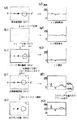
図1は本発明の実施の形態に係るマクロ検査装置の一例を示す概略構成図である。
【0018】
同図において、照明系に、干渉光源としてのハロゲンランプ等が用いられた白色光源21が設けられ、この白色光源21の前面には、フィルター回転ユニット22が配置されている。このフィルター回転ユニット22には、複数種類の干渉フィルター20が取り付けられ、被検査基板の観察に適合する単色光の取り出しを可能にしている。
【0019】
フィルター回転ユニット22を通った光は、光ファイバ23を介してフロスト24に与えられる。このフロスト24は、光ファイバ23からの光を拡散光に変換するものである。
【0020】
このフロスト24からの拡散光はハーフミラー25で反射してコリメートレンズ26に導き、ここで平行光に変換される。この平行光は、被検査対象である,レジスト等を塗布した基板27面に対し均一に一括照射される。
【0021】
この場合、基板27上に照射された光は、基板表面に塗布されて薄膜の上面と下面で反射し、膜厚に依存した干渉像を形成する。
一方、別途の照明系として、メタルハライドランプ41及びコリメートレンズ42が設けられている。メタルハライドランプ41から照射された光は、コリメートレンズ42にて平行光となり、斜め上方から基板27を一括照射する。
【0022】
この場合、基板27上に照射された光は、基板表面に形成されたパターンで回折を起こし、パターンに依存した回折像を形成する。また基板上の、ゴミ、キズといった欠陥も、この回折光学系で観察できる。
【0023】
これらの干渉像・回折像・ゴミ・キズ等の画像は、コリメートレンズ26、ハーフミラー25を通し、さらにズームレンズ28を通してCCDカメラ29に結像する。この結像カメラ29には、解像度の高いモノクロカメラが用いられている。
【0024】
次に、本マクロ検査装置の観察系、情報解析系の構成について説明する。
CCDカメラ29は、カメラコントローラ30を通して、画像処理装置31に接続されている。
【0025】
画像処理装置31は、複数枚の画像メモリM1〜Mnを備え、個々の被検査基板の合否判定を行う画像処理を実行するとともに、基本的には連続する1ロット20枚分の検査基板の画像を重ね合わせて重ね合わせ画像(加算蓄積画像ともいう)を作成する。
【0026】
なお、加算蓄積画像は、検査基板のトレンド解析を行うための情報として供するものであり、1ロット分または1ロットに至る途中の加算蓄積の画像及び設定により1ロットを越える多数の加算蓄積の画像も加算蓄積画像である。この加算蓄積画像は、単純加算またはシェーディング補正した画面の加算によって作成される。
【0027】
本実施形態では、画像の下地ムラを排除する為に生画像からシェーディング補正画像を作成し、加算蓄積する方法を採用している。また、完全なNG画像を加算してしまうとトレンドデータを壊してしまうので、画像処理装置31において、NG画像は加算しないようにプログラムされている。
【0028】
なお、単純加算する場合には、マクロ検査によって得られた生画像を加算したのち、一定濃度(加算した画像の平均濃度)を減算して加算蓄積画像を作成する。
【0029】
表示部32は、画像処理装置31に接続されたCRTモニタや液晶表示パネルからなり、被検査基板を1枚のマクロ画像として表示する他、上記重ね合わせ画像を表示する。
【0030】
ラインモニター35は、画像処理装置31に接続されており、重ね合わせ画像を常時モニター観察する場合に、当該画像を表示する専用の表示装置である。なお、加算蓄積画像の濃度断面画像も表示可能である。
【0031】
パソコン33は、画像処理装置31にて処理された情報を受け取るようになっている。また、マクロ検査装置の全体制御、検査結果の表示・統計解析、検査基板のロットNo.管理・製造装置No.レシピ管理などを行う。
【0032】
また、パソコン33は、被検査基板の画像や重ね合わせ画像の情報に基づく統計解析を実行し、本マクロ検査装置がプロセスモニターとして機能するようにしている。なお、パソコンに代えてワークステーション等の他の計算機手段を用いてもよい。
【0033】
モニター34は、パソコン33の表示用モニタである。
次に、以上のように構成された本発明の実施の形態に係るマクロ検査装置の動作について説明する。
【0034】
まず、本実施形態の装置は、従来の自動マクロ検査装置と同様に被検査基板1枚毎に画像処理を施して合否判定を行う。これにより自動的なマクロ検査が実行される。
【0035】
この他、本マクロ検査装置は、検査基板について画像重ね合わせを実行し、これを表示して検査員の判断に供するとともに、異常検出もしくは異常発生の予測を自動的に判定し通知しプロセスモニターとして動作する。
【0036】
以下、図2に従って加算蓄積画像の作成手順を示す。
図2は加算蓄積画像の作成及び異常検出もしくは異常予測の手順を示す図である。
【0037】
まず、画像処理装置31において、マクロ検査で得られた被検査画像(図2 (a1))を取り込み、画像メモリM1に記憶する。このときのxx´濃度断面を示すのが図2(a2)である。なお、図2(a2)には示さないが、ここで、濃度が所定の閾値を越えている場合には、当該被検査基板に異常が発生していると自動的に判断され通知される。
【0038】
次に、この被検査画像にスムージング処理を加えシェーディング画像(図2 (b1))を作成し画像メモリM2に記憶する。xx´濃度断面を図2(b2)に示す。なお、ここでスムージングをかけるのは、この画像の平均の濃度レベルを取り出すためである。
【0039】
次に、被検査画像M1からシェーディング画像M2を引き、シェーディング画像(図2(c1))として画像メモリM3に記憶する。図2(c2)に示すように、そのxx´濃度断面においては、画像全体の平均レベルが0となっている。
【0040】
次に、加算蓄積用画像メモリM4に画像メモリM3を加算する。こうして得られるのが加算蓄積画像(図2(d1))である。xx´濃度断面を図2(d2)に示す。なお、加算蓄積用画像メモリM4はロットの1枚目でクリアされる。さらに複数ロットにわたる長期間のトレンドデータを得たいときは、クリアせずに同じ基板種類のデータをそのまま加算してゆくよう設定する。
【0041】
次のロットの基板検査に移るまでは、新たな基板を検査する度に上記図2(a1)〜図2(d1)を繰り返し、加算蓄積画像についてさらに加算蓄積してゆくこととなる。
【0042】
以上の処理は画像処理装置31において行われているが、この加算蓄積画像はパソコン33に送出され、パソコン33にて解析処理が実行される。
個々の検査結果における濃度のばらつきがランダムであれば、加算蓄積画像上では特定位置のみの濃度が平均レベルからずれることはなく全体が平均化されるはずである。これに対しプロセスに異常もしくは異常検出されるほどではなくても正常状態からずれ始めている状態(以下、異常等ともいう)にあるときには、特定位置のみの濃度が平均レベルから常にずれている場合がある。
【0043】
したがって、パソコン33では、濃度レベルばらつきに対し閾値を設けて、加算蓄積画像がその閾値を越えたらその旨を通知するようにしている。このようにパソコン33における解析処理において、加算蓄積画像の濃度レベルのばらつきが濃度最大値のたとえば30%以上となれば注意信号を、40%以上では異常発生の危険信号をモニタ−34上に出力する。これらの閾値は、検査項目や被検体の種別等による解析条件に応じて変更することが可能である。なお、この解析処理における判断では、後述するように蓄積画像の濃度ヒストグラムが用いられる。
【0044】
これにより、複数マクロ画像に基づくトレンドデータによりプロセスモニタリングがなされることとなる。
一方、検査員の監視用に、画像処理装置31で作成された加算蓄積画像が、ラインモニター35あるいは表示部32から表示出力されている。
【0045】
この加算蓄積画像のラインモニター35あるいは表示部32からの表示時には、図2(d1)で作成された加算蓄積画像に一定の濃度(例えば濃度レベル100)を加え、見やすい画像に変換してから表示装置上に出力する(図2(e1))。なお、検査員の設定操作によりこの画像のxx´濃度断面を表示する場合もある(図2(e2))。
【0046】
このような加算蓄積画像がラインモニター35から表示された場合、同画像では同じ場所に現れた欠陥は加算した基板枚数倍の輝度レベルで表示される。従って、1枚の画像では認識できないような薄いムラであっても同じ位置に現れているものは次第に明るいムラとなって表示され、目視でも十分認識できる欠陥となって表示される。
【0047】
また、完全な良品基板のマクロ画像を蓄積してゆくとその生産ロットの膜厚のばらつきが見えてくる。膜厚のばらつきが一様であれば問題ないが、ある場所に偏って発生している場合には製造装置に問題があるのではないかと推測できる。このような問題点は、簡易には上記パソコン33の閾値レベル通知機能により検出することができ、さらに、図2(d1),図2(d2),図2(e1)あるいは図2(e2)の加算蓄積画像、濃度断面画像から具体的な異常,異常兆候を詳細検討することもできる。
【0048】
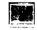
図3に本実施の形態のマクロ検査装置から得られる加算蓄積画像の一例を示す。また、図4に比較例としてミクロ検査装置から得られる欠陥マップの一例を示す。
【0049】
図3より、マクロ画像を蓄積することにより濃度ムラが生じていることがわかるが、一方、図4との比較により濃度ムラの発生状況はミクロ欠陥とは必ずしも対応していないことがわかる。このように本マクロ検査装置を用いれば、ミクロ検査装置では検出できないプロセス上の問題点をも検出できることがわかる。
【0050】
次に、本実施形態のマクロ検査装置を用いた工程の異常等の検出、異常解析のフィードバックについて説明する。
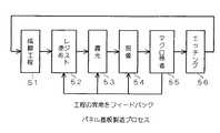
図5は、液晶パネル基板の製造プロセスを示す図である。
【0051】
パネル基板は、成膜工程51、レジスト塗布工程52、露光工程53、現像工程54、検査工程55(マクロ検査55)及びエッチング工程56を7〜8回繰り返すことによって完成する。
【0052】
この検査工程55では、レジスト塗布・露光・現像の各工程52,53,54における欠陥や異常を検査する。ここでNGと判断された基板は、レジストが剥離された後、レジスト塗布工程52からやり直される(リワークと呼ぶ)か又は廃棄される。
【0053】
マクロ検査装置は、レジスト塗布不良・露光不良・現像不良・ゴミ・搬送欠陥などのフォトリソ工程で生じた欠陥を捕まえる。そして、検出された欠陥内容は解析され分類されて、最終的には検査員が欠陥の発生原因をつきとめ、レジスト塗布・露光・現像の各工程52,53,54の製造装置にフィードバックすることになる。
【0054】
この過程において、本検査装置では、マクロ検査で得られた被検査基板の加算蓄積画像もが、ラインモニター35に表示される。したがって、検査員はこの加算蓄積画像による判定情報を目視確認し、プロセスモニタリングすることができる。
【0055】
さらに、上記したように、パソコン33による自動的な注意警報通知もなされる。
図6は加算蓄積画像の濃度ヒストグラムを示す図である。
【0056】
つまり、パソコン33の加算蓄積画像に対する自動解析機能が、図6に示す重ね合わせ画像の濃度ヒストグラムを取り、最大濃度と最小濃度の差が設定値(例えば40%)以上であった場合には、膜厚のばらつきが大きすぎと判断し、欠陥発生の前ぶれとして検査担当者や製造装置に注意信号を出力する。検査員はこの注意警報の通知情報も参考にしてプロセスモニタリングを行う。
【0057】
上述したように、本発明の実施の形態に係るマクロ検査装置及びプロセスモニタリング方法は、被検査基板の検査画像を重ね合わせて加算蓄積画像を作成し、これを統計処理、また解析してプロセスモニタリングするので、ロット基板に現れる共通欠陥を検出することができる。
【0058】
また共通欠陥の発生場所が特定できるため、欠陥の発生原因の追跡を容易に行うことができる。さらに、1枚の基板では認識できない薄いムラなどの欠陥も検出することができる。
【0059】
そして、個々の基板の良否にかかわらずそのマクロ画像を加算蓄積してモニター出力するので、膜厚ムラ等のばらつき具合から欠陥発生の前兆を把握することができ、欠陥の発生予測を行うことができる。
【0060】
このように、ウェハあるいは液晶ガラス基板等のフォトリソ工程において、欠陥発生を予測しその発生を事前にくい止めるように、生産装置を管理できるので、製造費用の削減及び生産効率の向上も図ることができる。
【0061】
なお、本発明は、上記各実施の形態に限定されるものでなく、その要旨を逸脱しない範囲で種々に変形することが可能である。
本実施形態では、連続する1ロット20枚分の検査基板の画像を重ね合わせて重ね合わせ画像を作成するとしたが、重ね合わせるべき枚数はこの枚数に限られるものでなく、適宜重ね合わせ数を変更調整することができる。
【0062】
さらに、本発明は、液晶パネル,PDP,FED等のフラットパネル用の基板や、半導体素子用ウェハ等の基板等、種々の基板の検査について適用することができる。
【0063】
また、実施形態に記載した手法は、計算機に実行させることができるプログラムとして、例えば磁気ディスク(フロッピーディスク、ハードディスク等)、光ディスク(CD−ROM、DVD等)、半導体メモリ等の記憶媒体に格納し、また通信媒体により伝送して頒布することもできる。本装置を実現する計算機は、記憶媒体に記録されたプログラムを読み込み、このプログラムによって動作が制御されることにより上述した処理を実行する。
【0064】
【発明の効果】
以上詳記したように本発明によれば、マクロ画像の加算蓄積画像を作成し解析するようにしたので、一枚単位では検出できない欠陥を検出したり、また良品基板しか流れていない場合でも、プロセスの微妙な変調を統計的に捕まえて欠陥の発生を時前に予測し欠陥発生を回避させることが可能なマクロ検査装置及びプロセスモニタリング方法を提供することができる。
【図面の簡単な説明】
【図1】本発明の実施の形態に係るマクロ検査装置の一例を示す概略構成図。
【図2】加算蓄積画像の作成及び異常検出もしくは異常予測の手順を示す図。
【図3】同実施の形態のマクロ検査装置から得られる加算蓄積画像の一例を示す図。
【図4】ミクロ検査装置から得られる欠陥マップの一例を示す比較図。
【図5】液晶パネル基板の製造プロセスを示す図。
【図6】加算蓄積画像の濃度ヒストグラムを示す図。
【符号の説明】
21…白色光源
22…フィルター回転ユニット
23…光ファイバ
24…フロスト
25…ハーフミラー
26…コリメートレンズ
27…基板
28…ズームレンズ
29…CCDカメラ
30…カメラコントローラ
31…画像処理装置
32…表示部
33…パソコン
34…モニター
35…ラインモニター
41…メタルハライドランプ
42…コリメートレンズ[0001]
BACKGROUND OF THE INVENTION
The present invention relates to a macro inspection apparatus and a process monitoring method for inspecting a surface defect of a subject in a production line or inspection line of a wafer or a liquid crystal glass substrate.
[0002]
[Prior art]
Non-uniform film thickness of resist applied to the substrate surface or adhesion of dust in flat panel such as liquid crystal panel, PDP (plasma display panel), FED (field emission display), etc. These defects appear as pattern line width defects after etching and pinholes in the pattern.
[0003]
In order to prevent such defects, a macro inspection and a micro inspection for inspecting a substrate before etching for defects are conventionally performed. Micro inspection is micro defect inspection and pattern inspection using a device with a resolution of about 5 μm. On the other hand, macro inspection is to detect defects of relatively large area such as film thickness unevenness, exposure failure, and resist coating failure. This is a targeted examination. In the macro inspection, thin unevenness that cannot be found in the micro inspection and defects due to continuous pattern deviation are detected. Moreover, since a wide visual field can be inspected collectively, there is an advantage that inspection can be performed in a short time.
[0004]
Currently, visual inspection is still the mainstream for macro inspection, but automatic inspection has also been performed. In this automatic inspection method, there is one in which image processing is performed for each substrate to be inspected to make a pass / fail determination, and Japanese Patent Application Laid- Open No. 07-027709 discloses such a technique.
[0005]
Further, regarding the defect contents detected by the inspection apparatus, Japanese Patent Application No. 06-157424 and Japanese Patent Application No. 06-234818 disclose a technique capable of discriminating defect types to some extent.
[0006]
[Problems to be solved by the invention]
However, the above macro inspection apparatus only makes a pass / fail determination for each sheet.
In this way, not only the pass / fail judgment of each sheet, but also the defect occurrence status of the substrate that flows continuously and the change in the macro image of the non-defective substrate are confirmed, so that abnormalities and modulation of the manufacturing process can be performed before the defect occurs. There is a request to detect.
[0007]
Moreover, in the conventional macro inspection apparatus, the defect determination is performed for each substrate to be inspected, but the defect analysis is not performed in units of lots (about 20 to 30) or more. Therefore, it is difficult to detect common defects between lots or defects that are thin and cannot be detected by a single substrate, and as a result of overlooking such defects, noticeable defects eventually occur and cause a decrease in yield. It was.
[0008]
That is, in the above case, since the inspection image of the non-defective substrate does not remain in the inspection apparatus, it is impossible to observe how the inspection image changes. Therefore, until the NG substrate flows, it is impossible to predict an abnormality in the manufacturing process, and many abnormal substrates flow during that time.
[0009]
Under such circumstances, it is desired to realize an (inline) process monitor for predicting the occurrence of defects / abnormalities in the production line based on the information of the macro inspection. Here, the process monitor refers to a manufacturing management system that monitors a manufacturing process using defect information obtained from a defect inspection apparatus.
[0010]
The present invention has been made in consideration of such circumstances, and detects defects that cannot be detected on a single sheet basis, or statistically captures subtle modulation of the process even when only non-defective substrates are flowing. An object of the present invention is to provide a macro inspection apparatus and a process monitoring method capable of predicting the occurrence of a defect in advance and avoiding the occurrence of the defect.
[0011]
[Means for Solving the Problems]
The essence of the present invention is to add and accumulate macro images to be inspected flowing from the manufacturing process to create an added accumulated image, and analyze the added accumulated image to statistically capture subtle modulation of the process, and to detect defects. The generation of defects is detected, and the occurrence of defects is predicted and avoided in advance.
[0012]
More specifically, the solution to the above problem is realized by the following solution. The present invention, taking an illuminating means for illuminating the inspected substrate manufactured by the board manufacturing process, an imaging unit for capturing a macro image of the illuminated said inspected substrate surface by the illumination means, by the image pickup means image processing means for creating an overlay image Mareta superimposed a plurality of macro images of the inspected substrate, before Symbol superimposition statistical processing or analyzing the information of the image, the common defect of the substrate to be inspected a macro inspection apparatus characterized by comprising a process monitoring means determines abnormality detection or occurrence of abnormality prediction of the manufacturing process due to.
Further, the present invention is illuminated by the illumination means with respect to the inspected substrate manufactured in board manufacturing process, macroscopically imaged by the imaging means illuminated the inspection substrate surface by said lighting means, the imaging means in creating an image overlay with ipecac to the image processing unit each macro image of the inspected substrate of a plurality captured, the superposition image statistical processing or analysis by ipecac to the computer unit, the each It is a process monitoring method characterized by determining an abnormality of the manufacturing process due to a common defect of an inspection substrate or a prediction of occurrence of the abnormality.
Further, continuously in board manufacturing process macroscopically imaging the surface of each test board are plural manufacturing, perform acceptance judgment for each Ma Kuroga image thus shooting the image of this, the result of this determination Abnormalities in the substrate manufacturing process by creating a superimposed image by superimposing a plurality of macro images excluding NG substrates determined to be reworked or discarded, and detecting common defects appearing at the same place in the superimposed image Alternatively , a process monitoring method is characterized in that a prediction of occurrence of an abnormality is determined .
[0013]
In the present invention, by providing such a configuration, for example, individual macro images can be continuously added and displayed, and macro defects and thin film thickness variations of a substrate to be inspected can be emphasized or detected. be able to. In other words, to detect defects that cannot be detected on a single sheet basis, or to predict the occurrence of defects by statistically capturing subtle modulation of the process even when only non-defective substrates are flowing, and avoiding the occurrence of defects Is possible.
[0014]
Next, the image processing means of the present invention adds the macro images of the substrates to be inspected taken from the imaging means, and then subtracts the average density of the added images to create the superimposed image It is characterized by doing.
The image processing means of the present invention is characterized in that a corrected macro image from which background unevenness has been removed is added to the macro image of each of the substrates to be inspected taken from the imaging means.
Further, the image processing means of the present invention creates a shading image obtained by smoothing processing and shading correction for each macro image of each inspection board , and adds an image obtained by subtracting the shading image from the macro image. It is characterized by.
[0015]
Image processing means of the present invention, to keep By providing such a configuration, since is subtracted in each smoothed image when creating a superimposed image, the average density level of the superimposed image to a predetermined value Can do. Therefore, without the density value of the superimposed image is immediately saturated, it is possible to create a more effective superimposed image.
[0017]
DETAILED DESCRIPTION OF THE INVENTION
Embodiments of the present invention will be described below.
FIG. 1 is a schematic configuration diagram showing an example of a macro inspection apparatus according to an embodiment of the present invention.
[0018]
In the drawing, a
[0019]
The light passing through the
[0020]
The diffused light from the
[0021]
In this case, the light irradiated on the
On the other hand, a
[0022]
In this case, the light irradiated onto the
[0023]
These images such as interference images, diffraction images, dust, and scratches are formed on the
[0024]
Next, the configuration of the observation system and information analysis system of the macro inspection apparatus will be described.
The
[0025]
The
[0026]
Note that the addition accumulation image is used as information for performing trend analysis of the inspection board, and an addition accumulation image for one lot or halfway to one lot and a number of addition accumulation images exceeding one lot depending on the setting. Is also an accumulated image. This addition accumulated image is created by simple addition or addition of a screen subjected to shading correction.
[0027]
In this embodiment, a method of creating a shading correction image from a raw image and adding and accumulating it in order to eliminate background unevenness of the image. Further, since the trend data is destroyed if a complete NG image is added, the
[0028]
In the case of simple addition, after adding the raw images obtained by the macro inspection, a certain density (average density of the added images) is subtracted to create an addition accumulated image.
[0029]
The
[0030]
The line monitor 35 is connected to the
[0031]
The
[0032]
Further, the
[0033]
The
Next, the operation of the macro inspection apparatus according to the embodiment of the present invention configured as described above will be described.
[0034]
First, the apparatus according to the present embodiment performs pass / fail determination by performing image processing for each substrate to be inspected, as in the conventional automatic macro inspection apparatus. As a result, automatic macro inspection is executed.
[0035]
In addition, this macro inspection apparatus performs image superposition on the inspection board, displays it for use by the inspector, and automatically determines and notifies abnormality detection or prediction of occurrence of abnormality as a process monitor. Operate.
[0036]
Hereinafter, a procedure for creating an addition accumulated image will be described according to FIG.
FIG. 2 is a diagram showing a procedure for creating an addition accumulated image and detecting an abnormality or predicting an abnormality.
[0037]
First, in the
[0038]
Next, a smoothing process is performed on the image to be inspected to create a shading image (FIG. 2 (b1)) and store it in the image memory M2. An xx ′ concentration cross section is shown in FIG. The reason why the smoothing is applied here is to take out the average density level of this image.
[0039]
Next, the shading image M2 is subtracted from the inspected image M1, and is stored in the image memory M3 as a shading image (FIG. 2 (c1)). As shown in FIG. 2C2, the average level of the entire image is 0 in the xx ′ density section.
[0040]
Next, the image memory M3 is added to the addition accumulation image memory M4. The addition accumulated image (FIG. 2 (d1)) is thus obtained. An xx ′ concentration cross section is shown in FIG. The addition accumulation image memory M4 is cleared at the first lot. Furthermore, when it is desired to obtain long-term trend data over a plurality of lots, the setting is made such that data of the same board type is added as it is without being cleared.
[0041]
Until the substrate inspection of the next lot is performed, each time a new substrate is inspected, the above-described FIG. 2 (a1) to FIG. 2 (d1) are repeated, and the addition accumulation image is further accumulated.
[0042]
The above processing is performed in the
If the variation in density in each test result is random, the density only at a specific position on the added accumulated image should not be deviated from the average level, and the whole should be averaged. On the other hand, when there is an abnormality in the process or when it is not detected to be abnormal, the concentration at a specific position may always deviate from the average level when the process starts to deviate from the normal state (hereinafter also referred to as an abnormality). is there.
[0043]
Therefore, the
[0044]
As a result, process monitoring is performed using trend data based on a plurality of macro images.
On the other hand, the addition accumulated image created by the
[0045]
At the time of displaying the added accumulated image from the line monitor 35 or the
[0046]
When such an added accumulated image is displayed from the
[0047]
In addition, as a macro image of a complete non-defective substrate is accumulated, the film thickness variation of the production lot becomes visible. If the variation in film thickness is uniform, there is no problem, but if it occurs in a certain place, it can be estimated that there is a problem in the manufacturing apparatus. Such a problem can be easily detected by the threshold level notification function of the
[0048]
FIG. 3 shows an example of an addition accumulated image obtained from the macro inspection apparatus according to the present embodiment. FIG. 4 shows an example of a defect map obtained from a micro inspection apparatus as a comparative example.
[0049]
From FIG. 3, it can be seen that density unevenness is caused by accumulating macro images. On the other hand, it can be seen from the comparison with FIG. 4 that the density unevenness does not necessarily correspond to micro defects. Thus, it can be seen that the present macro inspection apparatus can detect process problems that cannot be detected by the micro inspection apparatus.
[0050]
Next, detection of process abnormality using the macro inspection apparatus of the present embodiment and feedback of abnormality analysis will be described.
FIG. 5 is a diagram showing a manufacturing process of the liquid crystal panel substrate.
[0051]
The panel substrate is completed by repeating the
[0052]
In this inspection step 55, defects and abnormalities in the resist coating / exposure / development steps 52, 53 and 54 are inspected. The substrate determined to be NG here is restarted from the resist coating step 52 (referred to as rework) or discarded after the resist is peeled off.
[0053]
The macro inspection apparatus captures defects generated in the photolithography process such as resist application failure, exposure failure, development failure, dust, and transport defect. The detected defect contents are analyzed and classified, and finally, the inspector finds out the cause of the defect and feeds it back to the manufacturing apparatus in each of the resist coating / exposure / development steps 52, 53, and 54. Become.
[0054]
In this process, in the present inspection apparatus, the addition accumulated image of the inspected substrate obtained by the macro inspection is also displayed on the
[0055]
Further, as described above, an automatic caution warning notification is also made by the
FIG. 6 is a diagram showing a density histogram of the added accumulated image.
[0056]
That is, if the automatic analysis function for the added accumulated image of the
[0057]
As described above, in the macro inspection apparatus and the process monitoring method according to the embodiment of the present invention, the accumulated image is created by superimposing the inspection images of the substrate to be inspected, and this is statistically processed or analyzed to monitor the process. Therefore, the common defect appearing on the lot substrate can be detected.
[0058]
In addition, since the occurrence location of the common defect can be specified, the cause of the occurrence of the defect can be easily traced. Furthermore, defects such as thin unevenness that cannot be recognized by a single substrate can also be detected.
[0059]
Regardless of the quality of each substrate, the macro image is added and accumulated and output to the monitor, so it is possible to grasp the sign of defect occurrence from the degree of variation such as film thickness unevenness, and to predict the occurrence of defects. it can.
[0060]
In this way, in the photolithography process for wafers or liquid crystal glass substrates, etc., the production apparatus can be managed so as to predict the occurrence of defects and stop the occurrence in advance, so that manufacturing costs can be reduced and production efficiency can be improved. .
[0061]
In addition, this invention is not limited to said each embodiment, It can change variously in the range which does not deviate from the summary.
In the present embodiment, the image of the inspection substrate for 20 consecutive lots is superimposed to create a superimposed image. However, the number of sheets to be superimposed is not limited to this number, and the number of overlays can be changed as appropriate. Can be adjusted.
[0062]
Furthermore, the present invention can be applied to inspection of various substrates such as substrates for flat panels such as liquid crystal panels, PDPs, and FEDs, and substrates such as wafers for semiconductor elements.
[0063]
Further, the method described in the embodiment is stored in a storage medium such as a magnetic disk (floppy disk, hard disk, etc.), an optical disk (CD-ROM, DVD, etc.), a semiconductor memory, etc. as a program that can be executed by a computer. In addition, it can be transmitted and distributed by a communication medium. A computer that implements this apparatus reads a program recorded in a storage medium and executes the above-described processing by controlling the operation by this program.
[0064]
【The invention's effect】
As described above in detail, according to the present invention, since the addition accumulation image of the macro image is created and analyzed, it is possible to detect a defect that cannot be detected in a single unit, or even when only a non-defective substrate is flowing, It is possible to provide a macro inspection apparatus and a process monitoring method capable of statistically capturing subtle modulation of a process, predicting the occurrence of a defect in advance, and avoiding the occurrence of the defect.
[Brief description of the drawings]
FIG. 1 is a schematic configuration diagram showing an example of a macro inspection apparatus according to an embodiment of the present invention.
FIG. 2 is a diagram showing a procedure for creating an addition accumulated image and detecting an abnormality or predicting an abnormality.
FIG. 3 is a view showing an example of an addition accumulated image obtained from the macro inspection apparatus according to the embodiment;
FIG. 4 is a comparison diagram showing an example of a defect map obtained from a micro inspection apparatus.
FIG. 5 is a view showing a manufacturing process of a liquid crystal panel substrate.
FIG. 6 is a diagram showing a density histogram of an addition accumulated image.
[Explanation of symbols]
21 ... White
Claims (10)
この照明手段により照明された前記被検査基板表面のマクロ画像を取込む撮像手段と、
前記撮像手段により取込まれた複数枚の前記被検査基板のマクロ画像を重ね合わせた重ね合わせ画像を作成する画像処理手段と、
前記重ね合わせ画像の情報を統計処理又は解析し、前記各被検査基板の共通欠陥に起因する前記製造プロセスの異常検出もしくは異常発生の予測を判定するプロセスモニタリング手段と、
を備えたことを特徴とするマクロ検査装置。Illuminating means for illuminating the inspected substrate manufactured by the board manufacturing process,
Imaging means for capturing a macro image of the surface of the substrate to be inspected illuminated by the illumination means;
Image processing means for creating a superimposed image obtained by superposing macro images of the plurality of substrates to be inspected taken by the imaging means;
Statistical processing or analyzing the information before Symbol superimposed image, the process monitoring means for determining the prediction of abnormality detection or abnormality of the manufacturing process due to the common defect of the substrate to be inspected,
A macro inspection apparatus comprising:
前記照明手段により照明された前記検査基板表面を撮像手段によりマクロ的に撮像し、この撮像手段で撮像された複数枚の前記被検査基板の各マクロ画像を画像処理手段に取込んで重ね合わせ画像を作成し、
この重ね合わせ画像を計算機手段に取込んで統計処理又は解析し、前記各被検査基板の 共通欠陥に起因する前記製造プロセスの異常もしくは異常発生の予測を判定することを特徴とするプロセスモニタリング方法。Illuminated by the illumination means with respect to the inspected substrate manufactured in board manufacturing process,
The test substrate surface illuminated by said illuminating means macroscopically imaged by the imaging means, the image superimposed with ipecac a plurality of the macro image of the substrate to be inspected picked up by the image pickup means to the image processing unit Create
A process monitoring method characterized in that the superimposed image is taken into a computer means and subjected to statistical processing or analysis to determine an abnormality in the manufacturing process or a prediction of occurrence of the abnormality caused by a common defect of each substrate to be inspected .
Priority Applications (1)
| Application Number | Priority Date | Filing Date | Title |
|---|---|---|---|
| JP01869397A JP3752338B2 (en) | 1997-01-31 | 1997-01-31 | Macro inspection apparatus and process monitoring method |
Applications Claiming Priority (1)
| Application Number | Priority Date | Filing Date | Title |
|---|---|---|---|
| JP01869397A JP3752338B2 (en) | 1997-01-31 | 1997-01-31 | Macro inspection apparatus and process monitoring method |
Publications (2)
| Publication Number | Publication Date |
|---|---|
| JPH10221040A JPH10221040A (en) | 1998-08-21 |
| JP3752338B2 true JP3752338B2 (en) | 2006-03-08 |
Family
ID=11978713
Family Applications (1)
| Application Number | Title | Priority Date | Filing Date |
|---|---|---|---|
| JP01869397A Expired - Fee Related JP3752338B2 (en) | 1997-01-31 | 1997-01-31 | Macro inspection apparatus and process monitoring method |
Country Status (1)
| Country | Link |
|---|---|
| JP (1) | JP3752338B2 (en) |
Families Citing this family (12)
| Publication number | Priority date | Publication date | Assignee | Title |
|---|---|---|---|---|
| JP4623809B2 (en) * | 2000-09-29 | 2011-02-02 | Sumco Techxiv株式会社 | Wafer surface inspection apparatus and wafer surface inspection method |
| JP4733820B2 (en) * | 2000-09-05 | 2011-07-27 | Sumco Techxiv株式会社 | Defect wafer determination apparatus and determination method |
| JP4733252B2 (en) * | 2000-09-05 | 2011-07-27 | Sumco Techxiv株式会社 | Wafer surface inspection apparatus and inspection method |
| TW513772B (en) * | 2000-09-05 | 2002-12-11 | Komatsu Denshi Kinzoku Kk | Apparatus for inspecting wafer surface, method for inspecting wafer surface, apparatus for judging defective wafer, method for judging defective wafer and information treatment apparatus of wafer surface |
| JP2003100599A (en) * | 2001-09-25 | 2003-04-04 | Nikon Corp | Method for adjusting aligner and exposure system |
| GB2422202A (en) * | 2005-01-10 | 2006-07-19 | Univ East Anglia | A device for determining dust accumulation |
| JP2012184988A (en) * | 2011-03-04 | 2012-09-27 | Toray Eng Co Ltd | Testing apparatus and method for film thickness unevenness |
| KR20120129020A (en) * | 2011-05-18 | 2012-11-28 | 동우 화인켐 주식회사 | Apparatus and method for monitoring defect in film |
| JP2013008903A (en) * | 2011-06-27 | 2013-01-10 | Kyocera Corp | Test device and test method for solar cell element |
| JP5862422B2 (en) * | 2012-03-30 | 2016-02-16 | 大日本印刷株式会社 | Image processing apparatus, image processing program, and image processing method |
| JP5764592B2 (en) * | 2013-02-22 | 2015-08-19 | 東京エレクトロン株式会社 | Substrate processing apparatus, substrate processing apparatus monitoring apparatus, and substrate processing apparatus monitoring method |
| JP7021886B2 (en) * | 2017-09-19 | 2022-02-17 | 株式会社Screenホールディングス | Board inspection equipment, board processing equipment, board inspection method and board processing method |
-
1997
- 1997-01-31 JP JP01869397A patent/JP3752338B2/en not_active Expired - Fee Related
Also Published As
| Publication number | Publication date |
|---|---|
| JPH10221040A (en) | 1998-08-21 |
Similar Documents
| Publication | Publication Date | Title |
|---|---|---|
| JP5228490B2 (en) | Defect inspection equipment that performs defect inspection by image analysis | |
| JP3752338B2 (en) | Macro inspection apparatus and process monitoring method | |
| US6928185B2 (en) | Defect inspection method and defect inspection apparatus | |
| JP4902456B2 (en) | Unevenness evaluation apparatus, Unevenness evaluation method, Unevenness evaluation program, recording medium, and color filter manufacturing method | |
| JP6000356B2 (en) | Liquid crystal display panel inspection method and liquid crystal display panel inspection apparatus | |
| KR20060060742A (en) | Apparatus and method for automated web inspection | |
| JP2007194262A (en) | Defect judging system and substrate processing system | |
| JP2004061289A (en) | Pattern inspecting apparatus | |
| JP4804779B2 (en) | Over-detection prevention system and processing method for visual inspection of printed circuit board in film and tape form | |
| JP2004279244A (en) | Pattern inspection device | |
| JP2008190872A (en) | Surface defectiveness detector, surface defectiveness detecting method and program | |
| US7330042B2 (en) | Substrate inspection system, substrate inspection method, and substrate inspection apparatus | |
| JP2008096314A (en) | Macro inspection device | |
| JP2009204388A (en) | Defect inspection method | |
| JP4857917B2 (en) | Color filter appearance inspection method and appearance inspection apparatus | |
| JP5077887B2 (en) | Color filter defect correcting method and color filter defect correcting apparatus | |
| JP2008134160A (en) | Inspection device, inspection method, program and recording medium | |
| JPH10260139A (en) | Automatic inspection apparatus for substrate | |
| JP3803677B2 (en) | Defect classification apparatus and defect classification method | |
| JP2000292311A (en) | Method and device for inspecting unevenness in cyclic pattern | |
| JP2004117150A (en) | Pattern defect inspection device and pattern defect inspection method | |
| JP7059730B2 (en) | Inspection equipment and inspection method | |
| KR20060008609A (en) | Method for inspecting a wafer | |
| JPH08159984A (en) | Pattern irregularity inspecting apparatus | |
| JPH0894536A (en) | Device for identifying kind of defect and process management system |
Legal Events
| Date | Code | Title | Description |
|---|---|---|---|
| A977 | Report on retrieval |
Free format text: JAPANESE INTERMEDIATE CODE: A971007 Effective date: 20050808 |
|
| A131 | Notification of reasons for refusal |
Free format text: JAPANESE INTERMEDIATE CODE: A131 Effective date: 20050906 |
|
| A521 | Request for written amendment filed |
Free format text: JAPANESE INTERMEDIATE CODE: A523 Effective date: 20051101 |
|
| TRDD | Decision of grant or rejection written | ||
| A01 | Written decision to grant a patent or to grant a registration (utility model) |
Free format text: JAPANESE INTERMEDIATE CODE: A01 Effective date: 20051129 |
|
| A61 | First payment of annual fees (during grant procedure) |
Free format text: JAPANESE INTERMEDIATE CODE: A61 Effective date: 20051212 |
|
| FPAY | Renewal fee payment (event date is renewal date of database) |
Free format text: PAYMENT UNTIL: 20081216 Year of fee payment: 3 |
|
| FPAY | Renewal fee payment (event date is renewal date of database) |
Free format text: PAYMENT UNTIL: 20091216 Year of fee payment: 4 |
|
| FPAY | Renewal fee payment (event date is renewal date of database) |
Free format text: PAYMENT UNTIL: 20101216 Year of fee payment: 5 |
|
| LAPS | Cancellation because of no payment of annual fees |