JP3748761B2 - Reflector and reflective liquid crystal display device - Google Patents
Reflector and reflective liquid crystal display device Download PDFInfo
- Publication number
- JP3748761B2 JP3748761B2 JP2000201529A JP2000201529A JP3748761B2 JP 3748761 B2 JP3748761 B2 JP 3748761B2 JP 2000201529 A JP2000201529 A JP 2000201529A JP 2000201529 A JP2000201529 A JP 2000201529A JP 3748761 B2 JP3748761 B2 JP 3748761B2
- Authority
- JP
- Japan
- Prior art keywords
- reflector
- curved surface
- range
- degrees
- angle
- Prior art date
- Legal status (The legal status is an assumption and is not a legal conclusion. Google has not performed a legal analysis and makes no representation as to the accuracy of the status listed.)
- Expired - Fee Related
Links
Images


Description
【0001】
【発明の属する技術分野】
本発明は、外部光を光源とする反射型液晶表示装置に好適に使用できる反射体、およびこれを用いた反射型液晶表示装置に関する。さらに詳しくは、広範囲の角度にわたって良好な反射率を有すると共に、所望の範囲の反射方向において特に反射率を高めることのできる反射体、およびその反射体を用いることにより、広い視野角を有すると共に、ノート型パソコンのように特定の装置に組み込まれる表示装置の通常の視野範囲において、充分な明るさを確保できるよう、適度な指向性を有する反射型液晶表示装置に関するものである。
【0002】
【従来の技術】
近年、ハンディタイプのコンピュータなどの表示部として、特に消費電力が小さいことから外部光を光源とする反射型液晶表示装置が広く利用されている。この反射型液晶表示装置は、表示面側から入射した光を内部の反射体で表示面側に反射させて、液晶層の分子配列の状態に応じて示される表示を、利用者が目視できるようにするものである。
【0003】
この種の反射型液晶表示装置に用いられる反射体として、表面が平らな鏡面状態とされた反射体を用いると、入射角度に対応する特定の反射角度において非常に高い反射率を示すが、反射率の高い反射角度の範囲がきわめて狭い、すなわち、視野角が狭いという特性を持っている。そのため、反射体表面に球面の一部をなす凹部や溝を多数形成したり、ランダムな凹凸を設けたりすることにより、広範囲の方向に良好な反射率が得られるようにする試みがなされている(特願平9−203637号、特願平9−197576号、特願平9−194643号等)。
【0004】
このうち反射体表面に球面の一部をなす多数の凹部を設けたものとして、特願平9−203637号には、図8に示すような反射体が提案されている。この図に示す形態の反射体51は、例えばガラス等からなる基板52上に設けられた感光性樹脂層等からなる平板状の樹脂基材53(反射体用基材)の表面に、その内面が球面の一部をなす多数の凹部54が重なり合うように連続して形成され、その上に例えばアルミニウムや銀等の薄膜からなる反射膜55が蒸着または印刷等により形成されたものである。
【0005】
上記凹部54は、深さが0.1ないし3μmの範囲でランダムに形成されるとともに、隣接する凹部54のピッチも5ないし50μmの範囲でランダムに配置されている。また、凹部54の内面は、各々単一の球面の一部をなす曲面となっており、その傾斜角は、−18ないし+18度の範囲に設定されている。
【0006】
なお、上記の「凹部の深さ」とは反射体表面から凹部の底部までの距離、「隣接する凹部のピッチ」とは平面視したときに円形となる凹部の中心間の距離のことである。また、「凹部内面の傾斜角」とは、図9に示すように、凹部54の内面の任意の箇所において0.5μm幅の微小な範囲をとったときに、その微小範囲内における斜面の水平面に対する角度θのことである。角度θの正負は、反射体表面に立てた法線に対して例えば図8における右側の斜面を正、左側の斜面を負と定義する。
【0007】
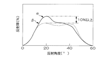
この反射体51は、図5のβに示すような反射特性を有している。図5は、入射角度30度において、縦軸を反射率(反射強度)、横軸を反射角度とした反射特性曲線を示すグラフである。なお、入射角度とは、図10に示すように、反射体51表面に立てた法線Hと入射光Jとがなす角度ω0である。また、反射角度とは、上記法線Hと入射光Jとを含む平面上において、上記法線Hと反射光Kとがなす角度ωである。図5のβに示すように、反射体51は、反射角度30度を中心として、15゜≦ω≦45゜の範囲で、ある程度良好な反射率を有しているものである。
【0008】
【発明が解決しようとする課題】
上述した従来の反射体51は、凹部の存在により比較的広範囲の角度にわたってある程度良好な反射率が得られるものである。しかし、図5のβに示すように反射角度15度および45度を左右のピークとして、反射角度30度を中心として、左右対称に反射強度の比較的高い領域が存在している。
【0009】
しかしながら、ノート型のパソコンのように、表示面を斜めにして使用する装置に組み込まれる表示装置は、表示面の傾斜の度合いや光源の位置によっても異なるが、図11に示すように、一般的に表示面に対する法線に近い方向から見られる場合が多い。図11は、本体61と蓋62を有するノート型パソコンを使用する状態を説明する図で、表示装置63は、蓋61の内面に設けられている。図11において、Pは、表示装置63に対する法線、Qは入射光、ω0は入射角度(たとえば30度)である。また、R1は反射角度ω0と入射角度ωとが等しい反射光、R2は、反射角度ω0が入射角度ωより小さい反射光、R3は、反射角度ω0が、入射角度ωより大きい反射光である。
【0010】
図から理解できるように、使用者の視線は通常法線Pに近い反射光R2の方向に集中する。これに対して、反射光R3は、表示装置63を下から見上げるような方向となり見づらいものである。したがって、使用者の利用の便宜を考えると、広い視野角を確保するのと同時に、反射角度の小さい方向の反射率をより高くすることが望まれる。
【0011】
反対に、テーブル型のゲーム機のように、水平面上の表示装置を見るような場合には、図12に示すように、一般的に表示面に平行する方向に近い方向から見られる場合が多い。図12は、テーブル72上に水平に設けられた表示装置73の使用状態について説明する図である。図12において、Wは、表示装置73に対する法線、Sは入射光、ω0は入射角度(たとえば30度)である。また、T1は反射角度ω0と入射角度ωとが等しい反射光、T2は、反射角度ω0が入射角度ωより小さい反射光、T3は、反射角度ω0が、入射角度ωより大きい反射光である。
【0012】
図から理解できるように、使用者の視線は通常反射光T1よりも反射角度の大きい反射光T3の方向に集中する。これに対して、反射光T2は、表示装置73を上から覗き込むような方向となり見づらいものである。したがって、使用者の利用の便宜を考えると、広い視野角を確保するのと同時に、反射角度の大きい方向の反射率をより高くすることが望まれる。
【0013】
本発明は、上記の問題を解決するためになされたものであって、広範囲の角度にわたって良好な反射率を有すると共に、入射角度よりも小さい反射角度(負の値を含む)や大きい反射角度等、所望の方向の反射率を重点的に高めることのできる反射体、およびその反射体を用いることにより、広い視野角を有すると共に、表示面を斜めや水平にして使用する場合等、特定の使用状況における通常の視野範囲に対して、適度な指向性を有する反射型液晶表示装置を提供することを課題とする。
【0014】
【課題を解決するための手段】
上記の課題を解決するために、本発明は、反射体表面に多数の凹部が形成され、前記凹部の内面が、各々半径の異なる2つの球面の一部である周縁曲面と周縁曲面に囲まれた位置に存する底曲面とを連続させた面からなり、かつ、前記凹部の内面が各々半径の異なる2つの球面から構成され、1つは周縁曲面とされ、他の1つは底曲面とされてなり、前記周縁曲面を形成する球面の断面における曲率半径が、底曲面を形成する球面の断面における曲率半径より小さいと共に、各々の球面の中心から反射体表面に立てた法線が、互いに異なる直線上に存することを特徴とする反射体を提供する。
また、本発明は、反射体表面に多数の凹部が形成され、前記凹部の内面が主の第1曲面部と、前記第1曲面部内に形成された第2曲面部からなり、前記第2曲面部の曲率中心が、前記第1曲面部の曲率中心と異なるとともに、前記第2曲面部の位置に応じて、外光の反射光の最大輝度方向が設定されてなることを特徴とする反射体を提供する。
【0015】
本反射体によれば、周縁曲面(第1曲面部)を形成する球面の曲率半径が小さく広範囲の傾斜角が得られるため、充分な広さの視野角が得られる。また、凹部の中心部から若干ずれた位置に存在する底曲面(第2曲面部)の曲率半径が大きく平面に近い曲線となるため、凹部の内面において特定の傾斜角の分布が高くなり、その結果、入射角度より大きい又は小さい方向の反射角度における反射率が最も高くなり、その方向をピークとして近傍の反射率も高くなる。
【0016】
この場合、本発明の如く、各々の球面の中心から反射体表面に立てた法線が、0.1〜10μmの範囲の間隔をもって離間していることが望ましい。これは、0.1μmより小さいと適度な指向性が出せなくなり、10μmより大きいと正反射の反射強度が著しく小さくなるためである。なお、各法線からの離間距離が大きいほど、入射角度と反射率が最も高くなる反射角度との差は大きくなる。
【0017】
また、各凹部の内面の傾斜角は、本発明の如く、周縁曲面については、10〜35度及び−35〜−10度の範囲で、底曲面については、4〜17度及び−17〜−4度の範囲とすることが望ましい。これは、周縁曲面の傾斜角が10〜35度及び−35〜−10度の範囲を超えると反射光の傾斜角が広がりすぎて反射強度が低下し、底曲面の傾斜角が4〜17度及び−17〜−4度の範囲を超えると、ある特定方向の反射率が充分高くならないためである。
【0018】
また、各凹部の深さは、本発明の如く0.1ないし3μmの範囲でランダムに形成することが望ましい。これは、0.1μmより小さいと、正反射が強くなり過ぎ、3μmを越えると、後行程で凹部を平坦化するときに凸部の表面が平坦化膜で埋めきれず、所望の反射特性が得られなくなるからである。また、深さをランダムにせず、一定の深さの凹部のみとすると、規則性が生じて光の干渉色が出て反射光が色付いてしまうという不具合があるからである。
【0019】
なお、前述のように、上記の「凹部の深さ」とは、反射体表面から凹部の底部までの距離のことである。また、「凹部内面の傾斜角」とは、図9を用いて説明したように、凹部の内面の任意の箇所において0.5μm幅の微小な範囲をとったときに、その微小範囲内における斜面の水平面に対する角度θのことである。角度θの正負は、反射体表面に立てた法線に対して例えば図8における右側の斜面を正、左側の斜面を負と定義する。
【0020】
各凹部の配置については、互いに離間させてもよいが、本発明の如く互いに連続して形成する事が望ましい。これにより、反射体表面全面に凹部を効率よく配置することができるので、凹部によって適度な指向性を保ちながら視野角を広げるという効果が最大限に発揮できる。
【0021】
また、他の配置としては本発明の如く、多数の凹部を多数の溝と共に反射体表面に形成することもできる。これにより、凹部による上記効果に加えて、溝によって、溝に垂直な方向の視野角を広げるという効果を併せ持つことができる。この場合、溝は、直線上でも曲線状でもよく、また、互いに任意の角度で交差しても差し支えない。また、凹部と溝は、互いの効果が失われない範囲の密度で各々形成するものとする。
【0022】
また、本発明として、先のいずれかに記載の反射体を備えたことを特徴とする反射型液晶表示装置を提供する。なお、反射体の設置形態としては、液晶セルの外側に設置する外付け型、あるいは液晶セルを構成する基板の内面に設置する内蔵型のいずれのタイプとしてもよい。
【0023】
本反射型液晶表示装置は、広い視野角を有すると共に、適度な指向性を備えるものである。したがって、ノート型パソコン等の特定の装置に組み込んだ場合に、使用者の通常の視野範囲にわたって、充分な明るさを確保できるものである。
【0024】
【発明の実施の形態】
以下、本発明の一実施の形態を図1ないし図5を参照して説明する。図1は本実施の形態の反射体を示す図である。この図に示すように、本実施の形態の反射体1は、例えばガラス等からなる基板2上に設けられた感光性樹脂層等からなる平板状の樹脂基材3(反射体用基材)の表面に、その内面が図2に示す特定形状をなす多数の凹部4が重なり合うように連続して形成され、その上に例えばアルミニウムや銀等の薄膜からなる反射膜5が蒸着または印刷等により形成されたものである。
【0025】
図2(a)は、凹部4の断面図、図2(b)は平面図である。この図に示すように、各凹部4の内面は、周縁曲面(第1曲面部)4aと、周縁曲面4aに囲まれた位置にある底曲面(第2曲面部)4bとから形成されている。周縁曲面4aは、中心をO1として曲率半径がR1である球面の一部である。また、底曲面4bは、中心をO2として曲率半径がR2である球面の一部である。各々の球面の中心であるO1とO2とから、反射体1の表面に立てた法線は、各々別個の直線L1、L2上に位置する。
【0026】
各々の曲率半径R1とR2とは、R1<R2の関係にあり、かつ10μm≦R1≦70μm、20μm≦R2≦100μmの範囲で変化するものである。また、図2(a)において、θ1は周縁曲面4aの傾斜角で、10゜≦θ1≦35゜および−35゜≦θ1≦−10゜の範囲で変化するものである。また、θ2は底曲面4bの傾斜角で、4゜≦θ2≦17゜および−17゜≦θ2≦−4゜の範囲で変化するものである。
【0027】
なお、平面方向から見た周縁曲面4aの半径r1及び底曲面4bの半径r2は、各々の曲率半径、R1,R2及び傾斜角θ1、θ2に応じて決まるものである。
【0028】
凹部4の深さdは0.1ないし3μmの範囲で各凹部毎にランダムな値をとる。凹部4の深さが3μmを超えると、後工程で凹部4を平坦化する場合に凸部の頂上が平坦化膜で埋めきれず、所望の平坦性が得られなくなり、0.1μmに満たないと、正反射が強くなり過ぎるからである。
【0029】
再び、図1に戻り、凹部4の配置等について説明する。隣接する凹部4のピッチは5ないし50μmの範囲でランダムに配置する。なぜなら、仮に隣接する凹部4のピッチに規則性があると、光の干渉色が出て反射光が色付いてしまうという不具合があるからである。また、隣接する凹部4のピッチが5μm未満の場合、反射体形成用母型の製作上の制約があり、加工時間が極めて長くなる、所望の反射特性が得られるだけの形状が形成できない、干渉光が発生する等の問題が生じるからである。また、反射体形成用母型の製作に使用し得るダイヤモンド圧子を用いる場合の実用上の観点から、隣接する凹部4のピッチを5ないし50μmとすることが望ましい。
【0030】
上記構成の反射体の製造方法に特に限定はないが、たとえば以下のように製造することができる。まず、図3(a)に示すように、例えば黄銅、ステンレス、工具鋼等からなる表面が平坦な平板状の母型基材7を転造装置のテーブル上に固定する。そして、先端が図2に示す凹部4に対応する特定形状のダイヤモンド圧子8で母型基材7の表面を押圧し、母型基材7を水平方向に移動させてはダイヤモンド圧子8を上下動させて押圧するという操作を多数回繰り返すことにより、深さや配列ピッチが異なる多数の凹部7aを母型基材7の表面に転造し、図3(b)に示すような反射体形成用母型9とする。
【0031】
図4に示すように、ここで用いる転造装置は、母型基材7を固定するテーブルが0.1μmの分解能で水平面内のX方向、Y方向に移動し、ダイヤモンド圧子8が1μmの分解能で鉛直方向(Z方向)に移動する機能を持つものである。そして、X方向、Y方向の移動距離を変化させることによって隣接する凹部のピッチを、Z方向の移動距離を変化させることによって各凹部の深さを変化させられるものである。なお、ダイヤモンド圧子8の先端は、径R2の部分が中心軸からそれて形成され、それよりもやや上方に、径R1の部分が形成されている。
【0032】
その後、図3(c)に示すように、母型9を箱形容器10に収納、配置し、容器10に例えばシリコーンなどの樹脂材料11を流し込んで、常温にて放置、硬化させ、この硬化した樹脂製品を容器10から取り出して不要な部分を切除し、図3(d)に示すように、母型9の型面をなす多数の凹部と逆の凹凸形状である多数の凸部を持つ型面12aを有する転写型12を作成する。
【0033】
次に、ガラス基板の上面に、アクリル系レジスト、ポリスチレン系レジスト、アジドゴム系レジスト、イミド系レジスト等の感光性樹脂液をスピンコート法、スクリーン印刷法、吹き付け法等の塗布法により塗布する。そして、塗布終了後、加熱炉またはホットプレート等の加熱装置を用いて基板上の感光性樹脂液を例えば80〜100℃の温度範囲で1分以上加熱するプリベークを行って基板上に樹脂基材3としての感光性樹脂層を形成する。ただし、用いる感光性樹脂の種類によってプリベーク条件は異なるため、上記範囲外の温度と時間で処理してもよいことは勿論である。なお、ここで形成する感光性樹脂層の膜厚は2〜5μmの範囲とすることが好ましい。
【0034】
その後、図2(e)に示すように、図2(d)に示した転写型12を用い、この転写型12の型面12aをガラス基板上の樹脂基材3に一定時間押し付けた後、転写型12を樹脂基材3から外す。このようにして、図2(f)に示すように、樹脂基材3の表面に転写型型面12aの凸部を転写して多数の凹部4を形成する。また、型押し時のプレス圧は用いる樹脂基材3の種類にあった値を選択することが好ましく、例えば30〜50kg/cm2 程度の圧力とするのがよい。プレス時間についても用いる樹脂基材3の種類にあった値を選択することが好ましく、例えば30秒〜10分程度の時間とする。
【0035】
その後、透明なガラス基板の裏面側から樹脂基材3を硬化させるための紫外線等の光線を照射し、樹脂基材3を硬化させる。ここで照射する紫外線等の光線は、上記種類の感光性樹脂層からなる樹脂基材3の場合、50mJ/cm2 以上の強度であれば樹脂基材3を硬化させるのに充分であるが、感光性樹脂層の種類によってはこれ以外の強度で照射してもよいことは勿論である。そして、プリベークで用いたのと同様の加熱炉、ホットプレート等の加熱装置を用いてガラス基板上の樹脂基材3を例えば240℃程度で1分以上加熱するポストベークを行ってガラス基板上の樹脂基材3を焼成する。
【0036】
最後に、樹脂基材3の表面に例えばアルミニウムをエレクトロンビーム蒸着等によって成膜して凹部の表面に沿って反射膜1を形成することにより、本実施の形態の反射体1が完成する。
【0037】
図5のαは、本実施の形態の反射体1について、入射角度30度(図2における右側の方向からの入射)において、縦軸を反射率(反射強度)、横軸を反射角度とした反射特性曲線を示すグラフである。このように、本実施の形態の反射体1においては、凹部4の内面に、半径の小さい球面の一部からなる周縁曲面(第1曲面部)4aが存在し、比較的絶対値の大きい傾斜角の範囲を与えるので、15゜≦ω≦45゜という広い範囲で良好な反射率を有している。また、半径の大きい球面の一部からなる底曲面(第2曲面部)4b、すなわち平坦面に近い曲面が偏在するので、特定の範囲の傾斜角を与える内面の割合が高くなる。その結果、入射角度である30度と対象な方向の反射角度30度よりも、小さい反射角度における反射率が最も高くなり、その方向をピークとしてその近傍の反射率も高くなっている。従来技術に係る反射体51と比較すると、反射角度20度における反射率は、10%以上高くなっている。即ち、底曲面(第2曲面部)の位置に応じて外光の反射光の最大輝方向が設定される。
【0038】
また、図示しないが、図2の左側の方向から入射した場合には、入射角度である30度と対象な方向の反射角度30度よりも、大きい反射角度における反射率が最も高くなり、その方向をピークとして近傍の反射率も高くなる。
【0039】
なお、本発明の反射体と従来技術の反射体との反射光全体の光量を比較した場合、両者に有意の差は存在しない。図5の反射特性αとβとを比較すると、αの方が全体の光量が大きいように見えるが、これは、比較実験における条件を厳密にそろえることが困難であるためである。
【0040】
また、上記の製造方法によれば、反射体形成用の母型9を製造する際には、ダイヤモンド圧子8を上下動させて母型基材7の表面を押圧するだけであるから、ダイヤモンド圧子8と母型基材7が擦れ合うようなことがない。その結果、ダイヤモンド圧子8先端の表面状態が母型9側に確実に転写され、圧子8の先端を鏡面状態としておけば母型9の凹部内面、ひいては反射体の凹部内面も容易に鏡面状態とすることができる。
【0041】
さらに、ポリエステル等の樹脂フィルムを加熱することで凹凸面を形成する方法と比較して、凹部の深さ、径、ピッチ等の寸法、凹部内面の表面状態等は全て制御されたものであり、高精度の転造装置の使用により反射体の凹部形状をほぼ設計通りに作成することができる。したがって、本方法によれば、作成する反射体の反射角度、反射効率等の反射特性が制御しやすいものとなり、所望の反射体を得ることができる。
【0042】
なお、上記製造方法として図3に示した凹部の転造パターンはほんの一例に過ぎず、適宜設計変更が可能なことは勿論である。また、反射体用基材、母型用基材等の各種基材の材料、転写型の構成材料等に関しても適宜変更が可能である。
【0043】
図6は本発明の他の実施の形態の反射体を示す図である。この図に示すように、本実施の形態の反射体31は、例えばガラス等からなる基板32上に設けられた感光性樹脂層等からなる平板状の樹脂基材33(反射体用基材)の表面に、ストライプ溝34が形成され、次いで、特定形状をなす多数の凹部35がランダムに形成され、その上に例えばアルミニウムや銀等の薄膜からなる反射膜36が蒸着または印刷等により形成されたものである。
【0044】
ここで、凹部35は、図2に示した凹部4と同様であり、その内面は、各々球面の一部である周縁曲面と、周縁曲面に囲まれた位置ににある底曲面とから形成されている。周縁曲面の半径と底曲面の半径との関係、各々の球面の中心から、反射体31の表面に立てた法線が同一の直線上に位置する点等、種々の条件も前記凹部4について記載したのと同様である。
【0045】
本実施形態によれば、凹部の視野角を広げ、かつ適度な指向性を備えることができるという上記効果に加えて、溝によって、溝に垂直な方向の視野角を広げるという効果を併せ持つことができる。
【0046】
次に、上記の反射体を備えたSTN(Super Twisted Nematic )方式の反射型液晶表示装置について説明する。
図7に示すように、この反射型液晶表示装置は、例えば厚さ0.7mmの一対の表示側ガラス基板13と背面側ガラス基板14との間に液晶層15を設け、表示側ガラス基板13の上面側にポリカーボネート樹脂やポリアリレート樹脂等からなる1枚の位相差板16を設け、さらに位相差板16の上面側に第1の偏光板17を配設している。また、背面側ガラス基板14の下面側には、第2の偏光板18、図1に示した本実施の形態の反射体1を順次設けている。
【0047】
反射体1は、第2の偏光板18の下面側に凹部4を形成した面が対向するように取り付けられ、第2の偏光板18と反射体1との間には、グリセリン等の光の屈折率に悪影響を与えることのない材料からなる粘着体19が充填されている。
両ガラス基板13、14の対向面側にはITO(インジウムスズ酸化物)等からなる透明電極層20、21がそれぞれ形成され、透明電極層20、21上にポリイミド樹脂等からなる配向膜22、23がそれぞれ設けられている。これら配向膜22、23等の関係により液晶層15中の液晶は240度捻れた配置となっている。
【0048】
また、前記背面側ガラス基板14と透明電極層21との間に、図示していないカラーフィルタを印刷等で形成することにより、この液晶表示装置をカラー表示できるようにしてもよい。
【0049】
本実施の形態の液晶表示装置においては、上述したように、反射体1自体が広い反射角度にわたる高い反射率と適度な指向性を兼ね備えているので、使用者が通常に表示面を見る方向を中心として、広い視野角と充分な明るさを兼ね備えた表示面とすることができる。
【0050】
なお、本実施の形態の反射型液晶表示装置では、反射体を第2の偏光板の外側に配設する、いわゆる外付けの反射体とする例を説明したが、背面側ガラス基板の対向面側に配設して内蔵型としてもよい。また、液晶表示装置の例としてSTN方式のもので説明したが、液晶層の液晶分子の捻れ角を90度に設定したTN(Twisted Nematic )方式の液晶表示装置にも本発明の反射体を適用し得ることは勿論である。
【0051】
【発明の効果】
以上詳細に説明したように、本発明の反射体においては、内面を、各々半径の異なる2つの球面の一部である周縁曲面と周縁曲面に囲まれた位置に存する底曲面とを連続させた面からなり、かつ、前記凹部の内面が各々曲率半径の異なる2つの球面から構成され、1つは周縁曲面とされ、他の1つは底曲面とされてなり、前記周縁曲面を形成する球面の曲率半径が、底曲面を形成する球面の曲率半径より小さいと共に、各々の球面の中心から反射体表面に立てた法線が、互いに異なる直線上に存するようにした多数の凹部を表面に形成したことにより、広範囲の反射角度に対して良好な反射率が得られると共に、適度な指向性も兼ね備えることができる。
本発明の反射体は、反射体表面に複数の凹部の内面が主の第1曲面部と第2曲面部からなり、第2曲面部の位置に応じて、外光の反射光の最大輝度方向が設定されてなるので、広範囲の反射角度に対して良好な反射率が得られると共に、適度な指向性も兼ね備えることができる。
また、本発明の反射型液晶表示装置によれば、上記のような優れた特性を持つ反射体を備えたことにより、広い視野角と、使用者の望む方向を中心に充分な明るさを備える液晶表示装置を実現することができる。
【図面の簡単な説明】
【図1】 本発明の一実施の形態である反射体を示す斜視図である。
【図2】 同、反射体の凹部4を示すもので(a)は断面図、(b)は平面図である。
【図3】 同、反射体の製造過程を順を追って示したプロセスフロー図である。
【図4】 同、反射体の形成に用いる母型の製造過程を示す図であって、ダイヤモンド圧子で母型基材を押圧している状態を示す図である。
【図5】 同、反射体と従来の反射対の反射特性との比較データである。
【図6】 本発明の他の実施の形態である反射体を示す斜視図である。
【図7】 本発明の一実施の形態である反射型液晶表示装置を示す断面図である。
【図8】 従来の反射体の一例を示す斜視図である。
【図9】 反射体の凹部内面の傾斜角を説明するための図である。
【図10】 入射角度と反射角度とを説明するための図である。
【図11】 ノート型パソコンに設けられた表示装置の使用状態を説明するための図である。
【図12】 水平に設けられた表示装置の使用状態について説明する図である。
【符号の説明】
1 反射体
2 基板
3 樹脂基材(反射体用基材)
4 凹部
4a 周縁曲面(第1曲面部)
4b 底曲面(第2曲面部)
5 反射膜
7 母型基材
8 ダイヤモンド圧子
9 反射体形成用母型
12 転写型[0001]
BACKGROUND OF THE INVENTION
The present invention relates to a reflector that can be suitably used for a reflective liquid crystal display device using external light as a light source, and a reflective liquid crystal display device using the same. More specifically, a reflector that has good reflectivity over a wide range of angles and can increase the reflectivity particularly in a desired range of reflection direction, and a wide viewing angle by using the reflector, The present invention relates to a reflective liquid crystal display device having appropriate directivity so that sufficient brightness can be secured in a normal visual field range of a display device incorporated in a specific device such as a notebook personal computer.
[0002]
[Prior art]
In recent years, a reflective liquid crystal display device using external light as a light source has been widely used as a display unit of a handheld type computer or the like because of particularly low power consumption. This reflection type liquid crystal display device reflects light incident from the display surface side to the display surface side by an internal reflector so that the user can see the display shown according to the molecular arrangement state of the liquid crystal layer. It is to make.
[0003]
When a reflector having a flat mirror surface is used as a reflector used in this type of reflective liquid crystal display device, it exhibits a very high reflectance at a specific reflection angle corresponding to the incident angle. The range of the reflection angle with a high rate is very narrow, that is, the viewing angle is narrow. For this reason, attempts have been made to obtain good reflectivity in a wide range of directions by forming a large number of concave portions and grooves forming a part of a spherical surface on the reflector surface, or providing random irregularities. (Japanese Patent Application Nos. 9-203637, 9-197576, 9-194463, etc.).
[0004]
Of these, a reflector as shown in FIG. 8 is proposed in Japanese Patent Application No. 9-203637, in which many concave portions forming a part of a spherical surface are provided on the reflector surface. The
[0005]
The
[0006]
Note that the “depth of the recess” is the distance from the reflector surface to the bottom of the recess, and the “pitch of the adjacent recess” is the distance between the centers of the recesses that are circular when viewed in plan. . In addition, as shown in FIG. 9, the “inclination angle of the inner surface of the concave portion” means a horizontal plane of the inclined surface within a minute range when a small range of 0.5 μm width is taken at an arbitrary position on the inner surface of the
[0007]
The
[0008]
[Problems to be solved by the invention]
The above-described
[0009]
However, as shown in FIG. 11, a display device incorporated in a device that is used with an inclined display surface, such as a notebook personal computer, varies depending on the degree of inclination of the display surface and the position of the light source. It is often seen from the direction near the normal to the display surface. FIG. 11 is a diagram for explaining a state in which a notebook computer having a
[0010]
As can be understood from the figure, the user's line of sight is reflected light R close to the normal normal P.2Concentrate in the direction of. In contrast, the reflected light RThreeIs a direction in which the
[0011]
On the other hand, when viewing a display device on a horizontal plane, such as a table-type game machine, as shown in FIG. 12, it is often viewed from a direction generally parallel to the display surface. . FIG. 12 is a diagram for explaining a use state of the
[0012]
As can be seen from the figure, the user's line of sight is usually reflected light T.1Reflected light T having a larger reflection angle thanThreeConcentrate in the direction of. In contrast, the reflected light T2Is a direction that looks into the
[0013]
The present invention has been made to solve the above-described problem, and has a good reflectance over a wide range of angles, and a reflection angle (including a negative value) smaller than the incident angle, a large reflection angle, and the like. Specific use such as a reflector that can increase the reflectivity in a desired direction, and a reflector that has a wide viewing angle and has a display surface inclined or horizontal. It is an object of the present invention to provide a reflective liquid crystal display device having appropriate directivity with respect to a normal visual field range in a situation.
[0014]
[Means for Solving the Problems]
In order to solve the above-mentioned problems, the present invention has a large number of recesses formed on the reflector surface, and the inner surface of the recess is surrounded by a peripheral curved surface and a peripheral curved surface, which are part of two spherical surfaces each having a different radius. Consists of a continuous surface with a bottom curved surface at a certain position,And the inner surface of the recess is composed of two spherical surfaces each having a different radius, one is a peripheral curved surface, and the other is a bottom curved surface,The spherical surface that forms the peripheral curved surfaceCurvature in cross sectionThe radius of the spherical surface forming the bottomCurvature in cross sectionProvided is a reflector having a smaller radius and normals standing on the reflector surface from the center of each spherical surface on different straight lines.
In the present invention, a plurality of concave portions are formed on the reflector surface, and the inner surface of the concave portion includes a main first curved surface portion and a second curved surface portion formed in the first curved surface portion, and the second curved surface. And a center of curvature of the first curved surface portion is different from that of the first curved surface portion, and a maximum luminance direction of reflected light of outside light is set according to a position of the second curved surface portion. I will provide a.
[0015]
According to this reflector, the spherical surface forming the peripheral curved surface (first curved surface portion)curvatureSince the radius is small and a wide range of tilt angles can be obtained, a sufficiently wide viewing angle can be obtained. In addition, the bottom curved surface (second curved surface portion) present at a position slightly deviated from the center of the concave portionLarge radius of curvatureSince the curve is close to a flat surface, the distribution of the specific inclination angle is high on the inner surface of the recess, and as a result, the reflectance at the reflection angle in the direction larger or smaller than the incident angle is the highest, Reflectivity also increases.
[0016]
in this case,The present inventionAs described above, it is desirable that the normals standing on the reflector surface from the center of each spherical surface are separated with an interval in the range of 0.1 to 10 μm. This is because when the thickness is smaller than 0.1 μm, appropriate directivity cannot be obtained, and when it is larger than 10 μm, the reflection intensity of regular reflection is remarkably reduced. Note that the greater the distance from each normal, the greater the difference between the incident angle and the reflection angle at which the reflectance is highest.
[0017]
The inclination angle of the inner surface of each recess isThe present inventionAs described above, it is desirable that the peripheral curved surface is in the range of 10 to 35 degrees and −35 to −10 degrees, and the bottom curved surface is in the range of 4 to 17 degrees and −17 to −4 degrees. This is because when the inclination angle of the peripheral curved surface exceeds the range of 10 to 35 degrees and −35 to −10 degrees, the inclination angle of the reflected light is excessively widened and the reflection intensity is lowered, and the inclination angle of the bottom curved surface is 4 to 17 degrees. And if it exceeds the range of -17 to -4 degrees, the reflectance in a specific direction is not sufficiently high.
[0018]
The depth of each recess isThe present inventionAs described above, it is desirable to form randomly within a range of 0.1 to 3 μm. If the thickness is smaller than 0.1 μm, the specular reflection becomes too strong. This is because it cannot be obtained. Further, if the depth is not random, but only the recesses of a certain depth are used, there is a problem in that regularity occurs and the interference color of light comes out and the reflected light is colored.
[0019]
As described above, the “depth of the recess” is a distance from the reflector surface to the bottom of the recess. In addition, the “inclination angle of the inner surface of the concave portion” means, as described with reference to FIG. 9, when a small range of 0.5 μm width is taken at an arbitrary position on the inner surface of the concave portion, The angle θ with respect to the horizontal plane. The positive / negative of the angle θ is defined, for example, such that the right slope in FIG. 8 is positive and the left slope is negative with respect to the normal line standing on the reflector surface.
[0020]
About the arrangement of each recess, they may be separated from each other,The present inventionIt is desirable to form them continuously as described above. Thereby, since a recessed part can be efficiently arrange | positioned in the reflector surface whole surface, the effect of extending a viewing angle can be exhibited to the maximum, maintaining moderate directivity by a recessed part.
[0021]
In addition, as other arrangementsThe present inventionAs described above, a large number of recesses can be formed on the reflector surface together with a large number of grooves. Thereby, in addition to the above-described effect due to the recess, the groove can have the effect of widening the viewing angle in the direction perpendicular to the groove. In this case, the grooves may be straight or curved, and may intersect with each other at an arbitrary angle. In addition, the recess and the groove are formed at a density within a range where the mutual effect is not lost.
[0022]
Also,BookAs an invention,AheadA reflective liquid crystal display device comprising the reflector according to any one of the above. In addition, as an installation form of the reflector, any of an external type installed outside the liquid crystal cell or a built-in type installed on the inner surface of the substrate constituting the liquid crystal cell may be used.
[0023]
The reflective liquid crystal display device has a wide viewing angle and appropriate directivity. Therefore, when incorporated in a specific device such as a notebook personal computer, sufficient brightness can be secured over the normal visual field range of the user.
[0024]
DETAILED DESCRIPTION OF THE INVENTION
Hereinafter, an embodiment of the present invention will be described with reference to FIGS. FIG. 1 is a diagram showing a reflector according to the present embodiment. As shown in this figure, the reflector 1 of the present embodiment is a flat resin base material 3 (reflector base material) made of a photosensitive resin layer or the like provided on a substrate 2 made of glass or the like, for example. 2 is formed continuously so that a large number of concave portions 4 having a specific shape shown in FIG. 2 overlap each other, and a reflective film 5 made of a thin film such as aluminum or silver is formed thereon by vapor deposition or printing. It is formed.
[0025]
2A is a cross-sectional view of the recess 4, and FIG. 2B is a plan view. As shown in this figure, the inner surface of each recess 4 is formed by a peripheral curved surface (first curved surface portion) 4a and a bottom curved surface (second curved surface portion) 4b located at a position surrounded by the peripheral
[0026]
EachcurvatureRadius R1And R2And R1<R2And 10 μm ≦ R1≦ 70μm, 20μm ≦ R2It changes within a range of ≦ 100 μm. In FIG. 2A, θ1Is the inclination angle of the peripheral
[0027]
The radius r of the peripheral
[0028]
The depth d of the recess 4 takes a random value for each recess in the range of 0.1 to 3 μm. If the depth of the concave portion 4 exceeds 3 μm, when the concave portion 4 is flattened in a subsequent process, the top of the convex portion cannot be filled with the flattening film, and the desired flatness cannot be obtained, and is less than 0.1 μm. This is because regular reflection becomes too strong.
[0029]
Returning to FIG. 1 again, the arrangement of the recesses 4 and the like will be described. The pitch of the adjacent recesses 4 is randomly arranged in the range of 5 to 50 μm. This is because, if the pitch between the adjacent recesses 4 is regular, there is a problem in that the interference color of light comes out and the reflected light is colored. Further, when the pitch of the adjacent recesses 4 is less than 5 μm, there are restrictions on the fabrication of the reflector forming matrix, the processing time becomes extremely long, and a shape sufficient to obtain the desired reflection characteristics cannot be formed, interference This is because problems such as generation of light occur. Further, from the practical point of view when using a diamond indenter that can be used for manufacturing a reflector forming matrix, it is desirable that the pitch of the adjacent recesses 4 be 5 to 50 μm.
[0030]
Although there is no limitation in particular in the manufacturing method of the reflector of the said structure, For example, it can manufacture as follows. First, as shown in FIG. 3A, a
[0031]
As shown in FIG. 4, the rolling device used here is such that the table for fixing the
[0032]
Thereafter, as shown in FIG. 3 (c), the mother die 9 is housed and arranged in a box-shaped
[0033]
Next, a photosensitive resin liquid such as an acrylic resist, a polystyrene resist, an azide rubber resist, and an imide resist is applied to the upper surface of the glass substrate by a coating method such as spin coating, screen printing, or spraying. Then, after the coating is finished, the photosensitive resin liquid on the substrate is prebaked at a temperature range of, for example, 80 to 100 ° C. for 1 minute or more using a heating apparatus such as a heating furnace or a hot plate, and the resin base material is formed on the substrate. A
[0034]
Thereafter, as shown in FIG. 2 (e), after using the
[0035]
Thereafter, light such as ultraviolet rays for curing the
[0036]
Finally, for example, aluminum is formed on the surface of the
[0037]
In FIG. 5, α represents the reflectance (reflection intensity) on the vertical axis and the reflection angle on the horizontal axis at an incident angle of 30 degrees (incident from the right direction in FIG. 2) for the reflector 1 of the present embodiment. It is a graph which shows a reflection characteristic curve. As described above, in the reflector 1 of the present embodiment, the peripheral curved surface formed of a part of a spherical surface having a small radius on the inner surface of the recess 4.(First curved surface part)4a exists and gives a range of inclination angles having a relatively large absolute value, and therefore has a good reflectance in a wide range of 15 ° ≦ ω ≦ 45 °. Also, a bottom curved surface consisting of a part of a spherical surface with a large radius(Second curved surface part)Since the curved surface close to 4b, that is, a flat surface is unevenly distributed, the ratio of the inner surface that gives a specific range of inclination angles increases. As a result, the reflectivity at a small reflection angle is the highest than the incident angle of 30 degrees and the reflection angle of 30 degrees in the target direction.ThatThe reflectance in the vicinity is also high. Compared with the
[0038]
Although not shown, when the light is incident from the left side of FIG. 2, the reflectance at the large reflection angle is the highest and higher than the incident angle of 30 degrees and the reflection angle of 30 degrees in the target direction. As a peak, the reflectance in the vicinity also increases.
[0039]
In addition, when the light quantity of the whole reflected light of the reflector of this invention and the reflector of a prior art is compared, there is no significant difference in both. When the reflection characteristics α and β in FIG. 5 are compared, it appears that α has a larger amount of light as a whole, but this is because it is difficult to strictly align the conditions in the comparison experiment.
[0040]
Further, according to the above manufacturing method, when manufacturing the mother die 9 for forming the reflector, the
[0041]
Furthermore, compared to the method of forming a concavo-convex surface by heating a resin film such as polyester, the depth, diameter, pitch and other dimensions of the recess, the surface state of the recess inner surface, etc. are all controlled, By using a high-precision rolling device, the concave shape of the reflector can be created almost as designed. Therefore, according to this method, the reflection characteristics such as the reflection angle and reflection efficiency of the reflector to be created can be easily controlled, and a desired reflector can be obtained.
[0042]
In addition, as a manufacturing method, the rolling pattern of the recesses shown in FIG. 3 is only an example, and it is needless to say that the design can be changed as appropriate. Further, various materials such as a reflector base material and a base material for a matrix, and a transfer type constituent material can be appropriately changed.
[0043]
FIG. 6 is a diagram showing a reflector according to another embodiment of the present invention. As shown in this figure, the
[0044]
Here, the
[0045]
According to the present embodiment, in addition to the above effect that the viewing angle of the recess can be widened and appropriate directivity can be provided, the groove can also have the effect of widening the viewing angle in the direction perpendicular to the groove. it can.
[0046]
Next, an STN (Super Twisted Nematic) type reflective liquid crystal display device having the above reflector will be described.
As shown in FIG. 7, this reflective liquid crystal display device is provided with a
[0047]
The reflector 1 is attached so that the surface on which the concave portion 4 is formed is opposed to the lower surface side of the second
Transparent electrode layers 20 and 21 made of ITO (Indium Tin Oxide) or the like are respectively formed on the opposing surface sides of the
[0048]
Further, a color filter (not shown) may be formed between the
[0049]
In the liquid crystal display device of the present embodiment, as described above, the reflector 1 itself has both high reflectivity over a wide reflection angle and appropriate directivity, so that the direction in which the user normally looks at the display surface can be changed. As a center, a display surface having a wide viewing angle and sufficient brightness can be obtained.
[0050]
In the reflective liquid crystal display device of the present embodiment, the example in which the reflector is a so-called external reflector disposed outside the second polarizing plate has been described. A built-in type may be provided on the side. Further, although the STN type has been described as an example of the liquid crystal display device, the reflector of the present invention is also applied to a TN (Twisted Nematic) type liquid crystal display device in which the twist angle of the liquid crystal molecules in the liquid crystal layer is set to 90 degrees. Of course you can.
[0051]
【The invention's effect】
As described above in detail, in the reflector according to the present invention, the inner surface is formed by connecting the peripheral curved surface, which is a part of two spherical surfaces having different radii, and the bottom curved surface located at the position surrounded by the peripheral curved surface. From the face,And the inner surface of the recess is composed of two spherical surfaces each having a different curvature radius, one is a peripheral curved surface, and the other is a bottom curved surface,The spherical surface that forms the peripheral curved surfacecurvatureThe radius of the spherical surface forming the bottomcurvatureThe surface is formed with a number of recesses that are smaller than the radius and whose normals standing on the reflector surface from the center of each spherical surface are on different straight lines. Reflectance can be obtained, and appropriate directivity can be provided.
In the reflector of the present invention, the inner surface of the plurality of recesses is mainly composed of the first curved surface portion and the second curved surface portion on the reflector surface, and the maximum luminance direction of the reflected light of the outside light according to the position of the second curved surface portion. Therefore, it is possible to obtain a good reflectivity with respect to a wide range of reflection angles and to have an appropriate directivity.
In addition, according to the reflective liquid crystal display device of the present invention, the reflector having the above-described excellent characteristics provides a wide viewing angle and sufficient brightness centered on the direction desired by the user. A liquid crystal display device can be realized.
[Brief description of the drawings]
FIG. 1 is a perspective view showing a reflector according to an embodiment of the present invention.
FIG. 2 shows the concave part 4 of the reflector, in which (a) is a sectional view and (b) is a plan view.
FIG. 3 is a process flow diagram showing the manufacturing process of the reflector step by step.
FIG. 4 is a view showing a manufacturing process of a mother die used for forming a reflector, and showing a state in which a mother die substrate is pressed with a diamond indenter.
FIG. 5 shows comparison data between the reflector and the reflection characteristics of a conventional reflection pair.
FIG. 6 is a perspective view showing a reflector according to another embodiment of the present invention.
FIG. 7 is a cross-sectional view showing a reflective liquid crystal display device according to an embodiment of the present invention.
FIG. 8 is a perspective view showing an example of a conventional reflector.
FIG. 9 is a view for explaining an inclination angle of an inner surface of a concave portion of a reflector.
FIG. 10 is a diagram for explaining an incident angle and a reflection angle.
FIG. 11 is a diagram for explaining a use state of a display device provided in a notebook personal computer.
FIG. 12 is a diagram illustrating a usage state of a horizontally provided display device.
[Explanation of symbols]
1 Reflector
2 Substrate
3 Resin base material (base material for reflector)
4 recess
4a Peripheral curved surface(First curved surface part)
4b Bottom curved surface(Second curved surface part)
5 Reflective film
7 Matrix base material
8 Diamond indenter
9 Reflector forming matrix
12 Transfer type
Claims (8)
Priority Applications (9)
| Application Number | Priority Date | Filing Date | Title |
|---|---|---|---|
| JP2000201529A JP3748761B2 (en) | 2000-07-03 | 2000-07-03 | Reflector and reflective liquid crystal display device |
| TW090112950A TW594218B (en) | 2000-07-03 | 2001-05-29 | Reflector and reflective liquid crystal display device |
| EP01305359A EP1174735A3 (en) | 2000-07-03 | 2001-06-20 | Reflector and reflection type liquid crystal display device using the same |
| US09/896,165 US6750930B2 (en) | 2000-07-03 | 2001-06-29 | Reflector providing particularly high reflectance in an intended viewing angle and reflection type liquid crystal display device using the same |
| CNB011199148A CN1210602C (en) | 2000-07-03 | 2001-06-29 | Reflector and reflecting liquid crystal display |
| KR10-2001-0039584A KR100425348B1 (en) | 2000-07-03 | 2001-07-03 | Reflector and reflective liquid crystal display |
| US10/668,878 US7123324B2 (en) | 2000-07-03 | 2003-09-23 | Reflector providing particularly high reflectance in an intended viewing angle and reflection type liquid crystal display device using the same |
| US10/668,929 US7515226B2 (en) | 2000-07-03 | 2003-09-23 | Reflector providing particularly high reflectance in an intended viewing angle and reflection type liquid crystal display device using the same |
| US10/895,773 US7471356B2 (en) | 2000-07-03 | 2004-07-21 | Reflector providing particularly high reflectance in an intended viewing angle and reflection type liquid crystal display device using the same |
Applications Claiming Priority (1)
| Application Number | Priority Date | Filing Date | Title |
|---|---|---|---|
| JP2000201529A JP3748761B2 (en) | 2000-07-03 | 2000-07-03 | Reflector and reflective liquid crystal display device |
Publications (3)
| Publication Number | Publication Date |
|---|---|
| JP2002022913A JP2002022913A (en) | 2002-01-23 |
| JP2002022913A5 JP2002022913A5 (en) | 2004-09-09 |
| JP3748761B2 true JP3748761B2 (en) | 2006-02-22 |
Family
ID=18699204
Family Applications (1)
| Application Number | Title | Priority Date | Filing Date |
|---|---|---|---|
| JP2000201529A Expired - Fee Related JP3748761B2 (en) | 2000-07-03 | 2000-07-03 | Reflector and reflective liquid crystal display device |
Country Status (1)
| Country | Link |
|---|---|
| JP (1) | JP3748761B2 (en) |
Families Citing this family (8)
| Publication number | Priority date | Publication date | Assignee | Title |
|---|---|---|---|---|
| JP2003215591A (en) * | 2002-01-25 | 2003-07-30 | Alps Electric Co Ltd | Transflective liquid crystal display device |
| US7567318B2 (en) | 2002-11-28 | 2009-07-28 | Alps Electric Co., Ltd. | Reflector and liquid crystal display panel |
| JP4211689B2 (en) * | 2004-06-14 | 2009-01-21 | オムロン株式会社 | Diffuser and surface light source device |
| JP2007206720A (en) * | 2007-04-06 | 2007-08-16 | Seiko Epson Corp | Reflector and manufacturing method therefor |
| WO2018088073A1 (en) * | 2016-11-14 | 2018-05-17 | 日本カーバイド工業株式会社 | Retroreflective sheet |
| JP2018084794A (en) * | 2016-11-14 | 2018-05-31 | 日本カーバイド工業株式会社 | Retroreflective sheet |
| WO2018088074A1 (en) * | 2016-11-14 | 2018-05-17 | 日本カーバイド工業株式会社 | Retroreflective sheet |
| JP2018084793A (en) * | 2016-11-14 | 2018-05-31 | 日本カーバイド工業株式会社 | Retroreflective sheet |
Family Cites Families (6)
| Publication number | Priority date | Publication date | Assignee | Title |
|---|---|---|---|---|
| JPH0887009A (en) * | 1994-09-20 | 1996-04-02 | Hitachi Ltd | Reflection type liquid crystal display device and reflection type color liquid crystal display device |
| JP3621226B2 (en) * | 1997-05-12 | 2005-02-16 | アルプス電気株式会社 | REFLECTOR, MANUFACTURING METHOD THEREOF, AND REFLECTIVE LIQUID CRYSTAL DISPLAY DEVICE USING THE SAME |
| JP3653164B2 (en) * | 1997-07-07 | 2005-05-25 | アルプス電気株式会社 | Reflector, method of manufacturing the same, and reflective liquid crystal display device |
| JP3547591B2 (en) * | 1997-07-29 | 2004-07-28 | アルプス電気株式会社 | Reflector and reflective liquid crystal display |
| JPH11242105A (en) * | 1998-02-24 | 1999-09-07 | Alps Electric Co Ltd | Matrix for forming reflector and its production and reflector and its production as well as reflection type liquid crystal display device |
| JP2000009910A (en) * | 1998-06-19 | 2000-01-14 | Sony Corp | Production of diffusion reflection plate and reflection display device |
-
2000
- 2000-07-03 JP JP2000201529A patent/JP3748761B2/en not_active Expired - Fee Related
Also Published As
| Publication number | Publication date |
|---|---|
| JP2002022913A (en) | 2002-01-23 |
Similar Documents
| Publication | Publication Date | Title |
|---|---|---|
| KR100425348B1 (en) | Reflector and reflective liquid crystal display | |
| KR100272883B1 (en) | Reflector having a convex and concave surface, netyhod of producing the reflector, and reflection-type lcd apparatus using the reflector | |
| KR100478574B1 (en) | Reflector and reflective liquid crystal display | |
| TW200422702A (en) | Collimating devices and devices having reflective and transmissive properties | |
| JPH11242105A (en) | Matrix for forming reflector and its production and reflector and its production as well as reflection type liquid crystal display device | |
| JP3748761B2 (en) | Reflector and reflective liquid crystal display device | |
| JP2005321610A (en) | Reflective bistable nematic liquid crystal display device | |
| JP3955191B2 (en) | Reflector and reflective liquid crystal display device | |
| JP2000298274A (en) | Reflection-type liquid crystal display device | |
| JP3694220B2 (en) | Reflector and reflective liquid crystal display device | |
| JP3612177B2 (en) | Method for manufacturing reflector forming mother die, method for manufacturing reflector, and method for manufacturing reflective liquid crystal display device | |
| JP3547591B2 (en) | Reflector and reflective liquid crystal display | |
| JP4159886B2 (en) | Reflector and liquid crystal display device | |
| JPH10311910A (en) | Reflection body and production therefor and reflection type liquid crystal display device | |
| JPH1144804A (en) | Reflector and reflection type liquid crystal display device | |
| JP3653164B2 (en) | Reflector, method of manufacturing the same, and reflective liquid crystal display device | |
| KR100272882B1 (en) | A reflector, a method for manufactuaring the same and reflective-type lcd device | |
| JP4028290B2 (en) | Liquid crystal display device and manufacturing method thereof | |
| JP3623341B2 (en) | Reflector and reflective liquid crystal display device | |
| JP3595549B2 (en) | Reflector and reflective liquid crystal display | |
| JP2005055762A (en) | Reflective body, liquid crystal display device, and method for manufacturing reflective body | |
| JP2003014913A (en) | Reflector and method for manufacturing the same, and liquid crystal display device | |
| JP2007506118A (en) | Reflective structure having diffuse reflection directivity and apparatus comprising the same | |
| JP2004054041A (en) | Reflector and reflection liquid crystal display device, and method for manufacturing reflector | |
| JP2005308789A (en) | Reflector and liquid crystal display device using the same |
Legal Events
| Date | Code | Title | Description |
|---|---|---|---|
| A977 | Report on retrieval |
Free format text: JAPANESE INTERMEDIATE CODE: A971007 Effective date: 20050114 |
|
| A131 | Notification of reasons for refusal |
Free format text: JAPANESE INTERMEDIATE CODE: A131 Effective date: 20050222 |
|
| A521 | Written amendment |
Free format text: JAPANESE INTERMEDIATE CODE: A523 Effective date: 20050425 |
|
| TRDD | Decision of grant or rejection written | ||
| A01 | Written decision to grant a patent or to grant a registration (utility model) |
Free format text: JAPANESE INTERMEDIATE CODE: A01 Effective date: 20051101 |
|
| A61 | First payment of annual fees (during grant procedure) |
Free format text: JAPANESE INTERMEDIATE CODE: A61 Effective date: 20051129 |
|
| R150 | Certificate of patent or registration of utility model |
Free format text: JAPANESE INTERMEDIATE CODE: R150 |
|
| FPAY | Renewal fee payment (event date is renewal date of database) |
Free format text: PAYMENT UNTIL: 20091209 Year of fee payment: 4 |
|
| FPAY | Renewal fee payment (event date is renewal date of database) |
Free format text: PAYMENT UNTIL: 20101209 Year of fee payment: 5 |
|
| FPAY | Renewal fee payment (event date is renewal date of database) |
Free format text: PAYMENT UNTIL: 20101209 Year of fee payment: 5 |
|
| FPAY | Renewal fee payment (event date is renewal date of database) |
Free format text: PAYMENT UNTIL: 20111209 Year of fee payment: 6 |
|
| LAPS | Cancellation because of no payment of annual fees |