JP3748005B2 - Display storage medium, image writing method, and image writing apparatus - Google Patents
Display storage medium, image writing method, and image writing apparatus Download PDFInfo
- Publication number
- JP3748005B2 JP3748005B2 JP00773399A JP773399A JP3748005B2 JP 3748005 B2 JP3748005 B2 JP 3748005B2 JP 00773399 A JP00773399 A JP 00773399A JP 773399 A JP773399 A JP 773399A JP 3748005 B2 JP3748005 B2 JP 3748005B2
- Authority
- JP
- Japan
- Prior art keywords
- display
- voltage
- period
- liquid crystal
- cholesteric liquid
- Prior art date
- Legal status (The legal status is an assumption and is not a legal conclusion. Google has not performed a legal analysis and makes no representation as to the accuracy of the status listed.)
- Expired - Fee Related
Links
Images


Description
【0001】
【発明の属する技術分野】
この発明は、画像(文字や図形などの情報を含む)を表示し、かつその表示状態を記憶する表示記憶媒体と、この表示記憶媒体に画像を書き込む方法および装置に関する。
【0002】
【従来の技術】
紙パルプの原料である森林資源の破壊や、ごみの廃却、焼却による環境汚染などから、オフィスを中心とする紙の大量消費が問題になっている。しかしながら、パーソナルコンピュータの普及や、インターネットを始めとする情報化社会の発達により、電子情報の一時的な閲覧を目的とする、いわゆる短寿命文書としての紙の消費は、益々増加する傾向にあり、紙に代わる書き換え可能な表示記憶媒体の実現が望まれている。
【0003】
【発明が解決しようとする課題】
そこで出願人は先に、特願平9−317049号(平成9年11月18日、出願)によって、無電源でのメモリ性を有し、外部装置によって短時間で画像を書き換えることができる、フルカラー表示可能な表示記憶媒体と、その画像書き込み方法および画像書き込み装置を提案した。
【0004】
この先願の発明では、表示記憶媒体として、一対の基板間に、それぞれブルー、グリーン、レッドの色光を選択反射し、図14に示すように、外部から印加される書き込み信号に対して、互いにしきい値電圧が異なるコレステリック液晶からなる表示層13A、13B、13Cを積層する。画像書き込み装置は、表示記憶媒体と別体に形成し、表示記憶媒体を挟持する一対の書き込み電極と駆動回路を設ける。
【0005】
そして、図15に示すように、リフレッシュ期間Trおよびセレクト期間Tsと、その後の無電圧の表示期間Tdとによって構成され、リフレッシュ期間Trおよびセレクト期間Tsでの印加電圧VrおよびVsが、Vr>Vsの関係をもって、各表示層のコレステリック液晶のしきい値電圧を境界とする7段階の電圧から選定された電圧となる書き込み信号を一対の書き込み電極間に印加して、画像を表示する。
【0006】
しかしながら、この先願の発明の表示記憶媒体と、その画像書き込み方法および画像書き込み装置では、図16に示すように(同図中の「p」はプレーナー組織による選択反射状態、「f」はフォーカルコニック組織による透過状態、をそれぞれ表し、図14のような特性の表示層13C、13B、13Aの順に示している)、上記のリフレッシュ電圧Vrおよびセレクト電圧Vsによって取り得る各表示層の配向状態の組み合わせは7種類であり、ホワイト、ブラック、ブルー、グリーンおよびレッドの5色と、各表示層のコレステリック液晶のしきい値電圧の大小によって決まる、シアン、イエローおよびマゼンタの3つの2次色のうちの2つ、の合計7色しか表示することができない。したがって、シアン、イエローおよびマゼンタの3つの2次色のうち、表示できない1色に関しては、1次色であるブルー、グリーンおよびレッドの並置混色で表現しなくてはならず、色再現域(色再現範囲)が狭くなってしまうという欠点がある。
【0007】
そこで、この発明は、無電源でのメモリ性を有し、外部装置によって短時間で画像を書き換えることができる、フルカラー表示可能な表示記憶媒体と、その画像書き込み方法および画像書き込み装置において、一画素内で、ホワイト、ブラック、ブルー、グリーン、レッド、シアン、イエローおよびマゼンタの8色を表示できるようにし、色再現域を拡大することを目的とするものである。
【0008】
【課題を解決するための手段】
請求項1の発明の表示記憶媒体は、
少なくとも、それぞれ可視光中の互いに異なる色光を選択反射するコレステリック液晶によって構成された複数の表示層が積層されるとともに、その複数の表示層に外部から印加される電圧に対して、その複数の表示層のコレステリック液晶のしきい値電圧が異なる表示記憶媒体において、
少なくとも前記複数の表示層の一つが、二周波駆動コレステリック液晶によって構成され、かつ、
前記二周波駆動コレステリック液晶のクロスオーバー周波数近傍の周波数の電圧が前記複数の表示層の外部から印加されたときに、前記二周波駆動コレステリック液晶によって構成された表示層がプレーナー組織からフォーカルコニック組織に配向変化することなく選択反射状態を維持する上限電圧が、前記二周波駆動コレステリック液晶によって構成された表示層と異なる表示層がプレーナー組織からフォーカルコニック組織に配向変化して透過状態となる下限電圧以上となるように構成されたことを特徴とする。
【0009】
請求項2の発明では、請求項1の表示記憶媒体に画像を書き込む方法として、前記複数の表示層の外部から、少なくとも、リフレッシュ期間、第1セレクト期間および第2セレクト期間と、その後の無電圧の表示期間とによって構成され、そのリフレッシュ期間での電圧Vrおよび第1セレクト期間での電圧Vs1がVr>Vs1の関係を有するとともに、少なくとも第1セレクト期間と第2セレクト期間での周波数が異なる書き込み信号を印加するものとする。
【0010】
請求項3の発明では、請求項1の表示記憶媒体に画像を書き込む装置として、前記複数の表示層の外部から、少なくとも、リフレッシュ期間、第1セレクト期間および第2セレクト期間と、その後の無電圧の表示期間とによって構成され、そのリフレッシュ期間での電圧Vrおよび第1セレクト期間での電圧Vs1がVr>Vs1の関係を有するとともに、少なくとも第1セレクト期間と第2セレクト期間での周波数が異なる書き込み信号を印加するものとする。
【0011】
【作用】
この発明によれば、表示記憶媒体は、少なくとも一つの表示層が、駆動周波数によって誘電異方性が大きく変化する二周波駆動コレステリック液晶によって構成されているため、印加する信号の周波数を変化させることにより、二周波駆動コレステリック液晶によって構成されている表示層と、それ以外の表示層との間で、それらの表示層を構成しているコレステリック液晶のしきい値電圧の相対的な関係を大きく変化させることができる。したがって、先願の発明と同様にして、リフレッシュ期間および第1セレクト期間の書き込み信号によって、3つの表示層を7種類の配向状態のいずれかに選択した後、先願の発明とは異なり、第2セレクト期間において、少なくとも2つの表示層に関して、それらの表示層を構成しているコレステリック液晶のしきい値電圧の大小関係を逆転させることができるような、第1セレクト期間とは異なる周波数の書き込み信号を印加することによって、先願の発明では選択できない残りの一つの配向状態を選択することが可能になり、色再現域を拡大することができる。
【0012】
【発明の実施の形態】
図1に、この発明の表示記憶媒体および画像書き込み装置の一実施形態を示す。
【0013】
表示記憶媒体1は、この実施形態では、基板2、3間に、表示面側(外光入射側)から、それぞれ可視光中の互いに異なる色光を選択反射するコレステリック液晶からなる3つの表示層8A、8B、8Cを、表示層8A、8B、8Cには、それぞれスペーサー7A、7B、7Cを挿入し、表示層8A、8B間には分離基板4を介し、表示層8B、8C間には分離基板5を介して積層し、非表示面側の基板3の裏面に光吸収層6を設けたものとする。
【0014】
基板2、3は、ガラスやシリコン、またはポリエステル(ポリエチレンテレフタレート)、ポリエーテルスルホン、ポリカーボネートなどの高分子フィルムを用いることができ、少なくとも表示面側の基板2は、光透過性を有する材料により形成する。
【0015】
基板2、3の厚みは、数10μm〜数100μmで、自己支持性と可とう性を併せ持つことが好ましい。また、表示層8A、8B、8Cへの分圧比を大きくするため、できるだけ誘電率の大きいことが好ましい。また、必要に応じて、その表面に、液晶配向層、耐摩耗層、表示記憶媒体1内へのガスの混入を防止するバリア層などの公知の機能性膜を形成してもよい。
【0016】
分離基板4、5は、基板2、3と同様の高分子フィルムを用いることができ、光透過性を有する材料により形成する。その厚みは、数μm〜数10μmで、可とう性を有することが好ましい。また、基板2、3と同様に、表示層8A、8B、8Cへの分圧比を大きくするため、できるだけ誘電率の大きいことが好ましい。また、必要に応じて、その表面に、液晶配向層などの公知の機能性膜を形成してもよい。
【0017】
スペーサー7A、7B、7Cは、ガラスやプラスチックなどからなるボール型またはシリンダー型のものを用いることができ、それぞれ表示層8A、8B、8Cの厚みを数μm〜数10μmに制御する。特に、基板2、3に可とう性を有する材料を用いる場合には、基板2、3の変形によって表示層8A、8B、8Cの厚みが大きく変化しないように、周囲に接着成分が塗布されたスペーサー7A、7B、7Cを用いて各基板間を接着し、あるいはスペーサー7A、7B、7Cの移動を防止することが好ましい。
【0018】
また、スペーサー7A、7B、7Cの代わりに、基板2、3および分離基板4、5の表面に、表示層8A、8B、8Cの厚みを制御しうる突起物などを形成してもよい。
【0019】
光吸収層6は、表示層8A、8B、8Cを透過した入射光を吸収するものであれば、特に限定されるものではなく、例えば、カーボンブラックなどの色素が含有された高分子膜を用いることができる。
【0020】
なお、非表示面側の基板3の裏面に光吸収層6を形成する代わりに、基板3と基板3上に形成される表示層8Cとの間に光吸収層6を形成し、または基板3に光吸収性を持たせて光吸収層6を省略することもできる。
【0021】
表示層8A、8B、8Cのうち少なくとも一層は、駆動周波数によってしきい値電圧が大きく変化するコレステリック液晶で構成する。このようなコレステリック液晶としては、例えば、分子短軸方向に極性基を有する3環以上の構造を持ち、駆動周波数によって誘電異方性が大きく変化する二周波駆動ネマチック液晶を主成分とする、低駆動周波数において正の誘電異方性を有するネマチック液晶に、ステロイド系コレステロール誘導体、あるいはシッフ塩基系、アゾ系、エステル系、ビフェニル系などのネマチック液晶の一部に光学活性基を導入したカイラルネマチック液晶をカイラル剤として添加した材料を用いることができる。
【0022】
表示層8A、8B、8Cのうち上記以外の表示層を構成するコレステリック液晶としては、ステロイド系コレステロール誘導体、あるいはシッフ塩基系、アゾ系、エステル系、ビフェニル系などのネマチック液晶の一部に光学活性基を導入したカイラルネマチック液晶、またはこれらを、シッフ塩基系、アゾ系、アゾキシ系、エタン系、ビフェニル系、ターフェニル系、シクロヘキシルカルボン酸エステル系、フェニルシクロヘキサン系、安息香酸エステル系、ピリミジン系、ジオキサン系、トラン系、シクロヘキシルシクロヘキサンエステル系、アルケニル系などの正の誘電率異方性を有するネマチック液晶、またはこれらの混合液晶に、カイラル剤として添加した材料を用いることができる。
【0023】
液晶分子が螺旋構造を持つコレステリック液晶は、入射光を右円偏光と左円偏光に分け、螺旋の捩じれ方向に一致する円偏光成分をブラッグ反射し、残りの光を透過させる選択反射現象を起こす。反射光の中心波長λ、および反射波長幅Δλは、螺旋ピッチをp、平均屈折率をn、複屈折率をΔnとすると、それぞれλ=n・p、Δλ=Δn・pで表され、コレステリック液晶層による反射光は螺旋ピッチに依存した鮮やかな色を呈する。
【0024】
正の誘電異方性を有するコレステリック液晶は、図12(A)に示すように、螺旋軸がセル表面に垂直になり、入射光に対して上記の選択反射現象を起こすプレーナー組織、同図(B)に示すように、螺旋軸がほぼセル表面に平行になり、入射光を少し前方散乱させながら透過させるフォーカルコニック組織、および同図(C)に示すように、螺旋構造がほどけて液晶ダイレクタが電界方向を向き、入射光をほぼ完全に透過させるホメオトロピック組織、の3つの状態を示す。
【0025】
上記の3つの組織のうち、プレーナー組織とフォーカルコニック組織は、無電圧で双安定に存在することができる。したがって、コレステリック液晶の配向状態は、液晶層に印加される電圧に対して一義的に決まらず、プレーナー組織が初期状態の場合には、印加電圧の増加に伴って、プレーナー組織、フォーカルコニック組織、ホメオトロピック組織の順に変化し、フォーカルコニック組織が初期状態の場合には、印加電圧の増加に伴って、フォーカルコニック組織、ホメオトロピック組織の順に変化する。
【0026】
一方、液晶層に印加した電圧を急激にゼロにした場合には、プレーナー組織とフォーカルコニック組織はそのままの状態を維持し、ホメオトロピック組織はプレーナー組織に変化する。
【0027】
したがって、パルス信号を印加した直後のコレステリック液晶層は、図13に示すような電気光学応答を示し、印加されたパルス信号の電圧が、Vfh,90以上のときには、ホメオトロピック組織からプレーナー組織に変化した選択反射状態となり、Vpf,10とVfh,10の間のときには、フォーカルコニック組織による透過状態となり、Vpf,90以下のときには、パルス信号印加前の状態を継続した状態、すなわちプレーナー組織による選択反射状態またはフォーカルコニック組織による透過状態となる。
【0028】
ただし、図中、縦軸は正規化反射率であり、最大反射率を100、最小反射率を0として、正規化している。また、反射率の変化には遷移領域が存在するため、正規化反射率が90以上の場合を選択反射状態、正規化反射率が10以下の場合を透過状態と定義し、プレーナー組織とフォーカルコニック組織のしきい値電圧を、遷移領域の前後に対して、それぞれVpf,90、Vpf,10とし、フォーカルコニック組織とホメオトロピック組織のしきい値電圧を、遷移領域の前後に対して、それぞれVfh,10、Vfh,90とする。
【0029】
コレステリック液晶の螺旋ピッチは、ネマチック液晶に対するカイラル剤の添加量で調整し、例えば、表示層8A、8B、8Cの選択反射光の中心波長が、それぞれ400〜500nm、500〜600nm、600〜700nmの範囲内になるようにする。ネマチック液晶に対するカイラル剤の溶解度が低く、上記範囲内の選択反射波長が得られない場合や、等方相転移温度が低下しすぎる場合には、複数のカイラル剤を添加する公知の手法を用いてもよい。また、コレステリック液晶の螺旋ピッチの温度依存性を補償するために、捩じれ方向が異なる、または逆の温度依存性を示す複数のカイラル剤を添加する公知の手法を用いてもよい。
【0030】
画像書き込み装置9は、表示記憶媒体1とは別体に形成し、この実施形態では、表示記憶媒体1を挟持する書き込み電極10、11と、この電極10、11間に書き込み信号を印加する駆動回路12とによって構成する。駆動回路12は、図では省略したが、駆動電源と、入力された画像データに基づいて、電極10、11間に印加する信号を制御する制御部とによって構成する。
【0031】
画像書き込み装置9は、例えば、電極10、11間に表示記憶媒体1の厚み分の間隔を有し、画像書き込み時には、その間隔内に表示記憶媒体1を所定位置まで差し込んで、後述するように表示記憶媒体1に画像を書き込み、または、電極10側を電極11側に対して開閉できるようにして、電極10側を開いて表示記憶媒体1を所定位置に挿入した後、電極10側を閉じて表示記憶媒体1に画像を書き込む、などの構成とすることができる。
【0032】
なお、この発明の画像書き込み装置9は、この発明の表示記憶媒体1に対して外部から、この発明の画像書き込み方法による書き込み信号を印加できるものであればよく、例えば、画素サイズの電極を備えるペン書き込み型の書き込み装置、一次元に電極が配置されたライン走査書き込み型の書き込み装置、二次元に電極が配置された面書き込み型の書き込み装置、またはこれらの形態でイオン流を発生させる表示装置など、特に限定されるものではない。
【0033】
図1の実施形態は、表示層8A、8B、8Cをコレステリック液晶のみからなる構造とした場合であるが、表示層8A、8B、8Cを、コレステリック液晶の連続相中に網目状の高分子を含むPNLC(Polymer Network Liquid Crystal)構造や、高分子の骨格中にコレステリック液晶がドロップレット状に分散されたPDLC(Polymer Dispersed Liquid Crystal)構造とすることもできる。
【0034】
表示層8A、8B、8CをPNLC構造やPDLC構造とすることによって、コレステリック液晶と高分子の界面にアンカリング効果が発生し、無電圧でのプレーナー組織またはフォーカルコニック組織の保持状態を安定にするとともに、スイッチング速度を向上させることができる。さらに、螺旋軸の揺らぎによって視野角が向上し、ソリッドな表示テクスチャを得ることができる。
【0035】
図2に、図1に示して上述した、この発明の表示記憶媒体1の等価回路を示す。
【0036】
図中、COおよびROは、表示層以外の構成要素の等価静電容量および等価抵抗値で、図1に示した実施形態では、基板2、3および分離基板4、5の、静電容量および抵抗値の直列和を示し、VOは、表示記憶媒体1に外部の画像書き込み装置9から電圧Vが印加された場合に、これら表示層以外の構成要素で発生する電圧降下を示す。通常、表示層以外の構成要素の等価抵抗値ROは十分に大きく、表示層以外の構成要素は絶縁体とみなすことができる。
【0037】
図中、CA、CB、CCおよびRA、RB、RCは、それぞれ表示層8A、8B、8Cの静電容量および抵抗値を示し、VA、VB、VCは、表示記憶媒体1に外部の画像書き込み装置9から電圧Vが印加された場合に、表示層8A、8B、8Cのそれぞれに実際に印加される電圧を示す。通常、表示層8A、8B、8Cの抵抗値RA、RB、RCは十分に大きく、また、静電容量CA、CB、CCは、液晶が誘電異方性を有することから、液晶の配向状態に依存して変化する。
【0038】
表示記憶媒体1に外部の画像書き込み装置9から電圧Vが印加された場合、各表示層8A、8B、8Cに実際に印加される電圧VA、VB、VCは、以下のようになる。
【0039】
VA=(C/CA)V …(1)
VB=(C/CB)V …(2)
VC=(C/CC)V …(3)
ここで、
C=CACBCCCO/(CACBCC+CACBCO+CACCCO+CBCCCO) …(4)
である。
【0040】
このように、この発明の表示記憶媒体1に対して、外部の画像書き込み装置9から任意の電圧を印加した場合、各表示層8A、8B、8Cには、それぞれ上記のような静電容量分圧による電圧が印加され、それぞれ、その電圧に応じて、各表示層8A、8B、8Cのコレステリック液晶の配向状態が変化する。
【0041】
したがって、この発明の表示記憶媒体1においては、外部の画像書き込み装置9から印加される電圧Vの、各表示層8A、8B、8Cへの分配比と、実際に印加される電圧VA、VB、VCに対する各表示層8A、8B、8Cの電気光学応答との、2つを制御することによって、外部の画像書き込み装置9から印加された電圧Vに対する各表示層8A、8B、8Cの電気光学応答を、所望の構成にすることができる。
【0042】
具体的には、前者の、各表示層8A、8B、8Cへの分配比は、上記のように各表示層8A、8B、8Cの静電容量比によって、後者の、各表示層8A、8B、8Cの電気光学応答は、各表示層8A、8B、8Cを構成するコレステリック液晶の誘電異方性、弾性率および螺旋ピッチ、さらに高分子を添加した場合には、高分子の構造や相分離プロセスなどに影響を受ける高分子と液晶の界面におけるアンカリング効果の程度などによって、制御することができる。
【0043】
さらに、外部の画像書き込み装置9から印加される書き込み信号の周波数によって、各表示層8A、8B、8Cを構成するコレステリック液晶の誘電率および誘電異方性が変化し、各表示層8A、8B、8Cの静電容量比および電気光学応答が変化するため、外部の画像書き込み装置9から印加される書き込み信号の周波数を制御することによって、外部の画像書き込み装置9から印加される電圧Vに対する各表示層8A、8B、8Cの電気光学応答を、所望の構成にすることができる。
【0044】
図3に、表示層8Cをクロスオーバー周波数fcの二周波駆動コレステリック液晶で構成した表示記憶媒体の、外部の画像書き込み装置9によって印加されたfcより低い周波数faの書き込み信号に対する、各表示層8A、8B、8Cの電気光学応答を示す。周波数faは直流を含む。
【0045】
周波数faの書き込み信号に対して、この表示記憶媒体は、3つの表示層8A、8B、8Cの、選択反射状態と透過状態の間の遷移領域が、同じ印加電圧で存在しないように構成する。しきい値電圧が最も大きい表示層を8A、中間の表示層を8B、最も小さい表示層を8Cとした場合、電圧Va、Vb、Vc、Vd、Ve、Vf、Vgを、
Va:表示層8CのVpf,90以下の電圧、
Vb:表示層8CのVpf,10と表示層8BのVpf,90との間の電圧、
Vc:表示層8BのVpf,10と表示層8AのVpf,90との間の電圧、
Vd:表示層8AのVpf,10と表示層8CのVfh,10との間の電圧、
Ve:表示層8CのVfh,90と表示層8BのVfh,10との間の電圧、
Vf:表示層8BのVfh,90と表示層8AのVfh,10との間の電圧、
Vg:表示層8AのVfh,90以上の電圧、
とする。
【0046】
図4に、表示層8Cをクロスオーバー周波数fcの二周波駆動コレステリック液晶で構成した表示記憶媒体の、外部の画像書き込み装置9によって印加されたfc近傍の周波数fbの書き込み信号に対する、各表示層8A、8B、8Cの電気光学応答を示す。
【0047】
周波数fbの書き込み信号に対して、この表示記憶媒体は、少なくとも表示層8A、8Bの、プレーナー組織からフォーカルコニック組織への配向変化に伴う選択反射状態と透過状態の間の遷移領域が、同じ印加電圧で存在しないとともに、表示層8Cが配向変化を生じない不感帯の上限電圧Vpf,90が、表示層8BのVpf,10以上になるように構成する。
【0048】
電圧Vh、Viは、
Vh:表示層8BのVpf,90以下の電圧、
Vi:表示層8Cの不感帯で、かつ表示層8BのVpf,10と表示層8AのVpf,90との間の電圧、
とする。
【0049】
なお、図4は表示層8Cの誘電異方性が正になるfb<fcの場合で、fb=fcの場合には、表示層8Cの誘電異方性が無くなって、全ての印加電圧領域が不感帯になり、表示層8Cの誘電異方性が負になるfb>fcの場合には、図4に示すfb<fcの場合とは逆に、フォーカルコニック組織からプレーナー組織への配向変化が不感帯の上限で生じる。
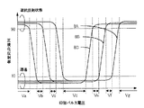
【0050】
そして、外部の画像書き込み装置9によって、図5に示すような、少なくとも、それぞれ周波数faのリフレッシュ期間Trおよび第1セレクト期間Ts1と、周波数fbの第2セレクト期間Ts2と、その後の無電圧の表示期間Tdとによって構成され、そのリフレッシュ期間Trでの電圧Vrおよび第1セレクト期間Ts1での電圧Vs1が、Vr>Vs1の関係をもって、入力画像データに基づいて、上記の周波数faにおける7段階の電圧Va〜Vgから選定された電圧となるとともに、第2セレクト期間Ts2での電圧Vs2が、上記の周波数fbにおける2段階の電圧Vh、Viから選定された電圧となる書き込み信号を、上記の表示記憶媒体に印加する。
【0051】
図6は、この場合のリフレッシュ電圧Vr、第1セレクト電圧Vs1および第2セレクト電圧Vs2の組み合わせによる、表示層8A、8B、8Cの配向状態を示したもので、「p」はプレーナー組織による選択反射状態、「f」はフォーカルコニック組織による透過状態、「?」は書き込み信号の印加前の状態に依存する未確定状態、をそれぞれ表し、表示層8C、8Bおよび8Aの順に示している。
【0052】
これから明らかなように、上記の表示記憶媒体および画像書き込み方法によれば、
(1)表示層8A、8Bおよび8Cの3層全てがプレーナー組織の状態、
(2)表示層8A、8Bおよび8Cの3層全てがフォーカルコニック組織の状態、
(3)表示層8Aがプレーナー組織で、表示層8Bおよび8Cがフォーカルコニック組織の状態、
(4)表示層8Bがプレーナー組織で、表示層8Aおよび8Cがフォーカルコニック組織の状態、
(5)表示層8Cがプレーナー組織で、表示層8Aおよび8Bがフォーカルコニック組織の状態、
(6)表示層8Aおよび8Bがプレーナー組織で、表示層8Cがフォーカルコニック組織の状態、
(7)表示層8Bおよび8Cがプレーナー組織で、表示層8Aがフォーカルコニック組織の状態、
(8)表示層8Aおよび8Cがプレーナー組織で、表示層8Bがフォーカルコニック組織の状態、
の8種類の配向状態が得られる。
【0053】
したがって、例えば、表示層8Aをブルーの色光、表示層8Bをグリーンの色光、表示層8Cをレッドの色光、をそれぞれ選択反射するように構成した場合には、図7に示すように(同図中の「T」は、対応する層がフォーカルコニック組織による透過状態であることを示す)、
(1)Vr=Vg、Vs1=Va、Vs2=Vhの書き込み信号によって、ホワイト(W)が表示される状態、
(2)例えば、Vr=Ve、Vs1=Vc、Vs2=Vhの書き込み信号によって、ブラック(Bk)が表示される状態、
(3)例えば、Vr=Vg、Vs1=Vc、Vs2=Vhの書き込み信号によって、ブルー(B)が表示される状態、
(4)Vr=Vf、Vs1=Vb、Vs2=Vhの書き込み信号によって、グリーン(G)が表示される状態、
(5)例えば、Vr=Ve、Vs1=Va、Vs2=Vhの書き込み信号によって、レッド(R)が表示される状態、
(6)Vr=Vg、Vs1=Vb、Vs2=Vhの書き込み信号によって、シアン(C)が表示される状態、
(7)Vr=Vf、Vs1=Va、Vs2=Vhの書き込み信号によって、イエロー(Y)が表示される状態、
(8)Vr=Vg、Vs1=Va、Vs2=Viの書き込み信号によって、マゼンタ(M)が表示される状態、
の8つの表示状態を取りうるようになり、一画素内で、ホワイト、ブラック、ブルー、グリーン、レッド、シアン、イエローおよびマゼンタの8色を表示することができる。
【0054】
さらに、ディザ法や誤差拡散法などの面積階調を行うことによって、フルカラー表示を行うことができる。
【0055】
なお、それぞれブルー、グリーンおよびレッドの色光を選択反射する表示層の積層順序、またはしきい値電圧の大小は、上記の例に限らず、任意に構成することができる。
【0056】
また、この発明は、コレステリック液晶からなる3つの表示層8A、8B、8Cに対して一括に電圧を印加する構成の全てに適用することができ、例えば、基板2、3の内面に駆動電極を有する実施形態、基板2、3の内面に駆動電極および光導電層を有し、画像書き込み装置から光導電層に照射される光量を制御することによって、画像書き込み装置から駆動電極間に書き込み信号が印加された場合の表示層全体に実際に印加される電圧を制御する実施形態、などとすることができる。
【0057】
(実施例1)
レッドの表示層を構成するコレステリック液晶として、二周波駆動ネマチック液晶(チッソ社製DF−02XX)を81.0wt%、カイラル剤1(メルク社製S811)を15.2wt%、カイラル剤2(メルク社製S1011)を3.8wt%の割合で混合した。
【0058】
グリーンの表示層を構成する材料として、ネマチック液晶1(メルク社製ZLI4389)を7.4wt%、ネマチック液晶2(メルク社製MLC2038)を66.8wt%、カイラル剤1(メルク社製CB15)を21.5wt%、カイラル剤2(メルク社製R1011)を4.3wt%の割合で混合したコレステリック液晶に、高分子前駆体(ノーランド社製NOA65)を15.0wt%の割合で添加した。
【0059】
積層状態では、各表示層の特性を個別に評価することができないため、この実施例では、レッドの表示層からなる表示セル、およびグリーンの表示層からなる表示セルを作製し、表示層が積層された場合と電気的に等価になるように、各表示セルを直列に接続した状態で画像の書き込みを行い、この発明の原理を検証した。
【0060】
ITO透明電極をスパッタ蒸着した1.1mm厚の一対のガラス基板(コーニング社製7059)に、垂直配向ポリイミド(日産化学社製SE7511L)を塗布形成し、一方のガラス基板の裏面に、ブラック樹脂(日本化薬社製BKR105)の光吸収層をスピンコートした後、5μm径の球状スペーサー(積水ファインケミカル社製ミクロパールSP−205)を介して空セルとした。これに、100℃のホットプレート上で、上記レッドのコレステリック液晶を毛管注入して、レッド表示セルを得た。
【0061】
同様に、ITO透明電極をスパッタ蒸着した1.1mm厚の一対のガラス基板(コーニング社製7059)を、一方のガラス基板の裏面にブラック樹脂(日本化薬社製BKR105)の光吸収層をスピンコートした後、5μm径の球状スペーサー(積水ファインケミカル社製ミクロパールSP−205)を介して空セルとした。これに、80℃のホットプレート上で、上記グリーンのコレステリック液晶に高分子前駆体が添加された材料を毛管注入し、表示面側から50mW/cm2(365nm)のUV光を30秒間照射して、グリーン表示セルを得た。
【0062】
各表示セルの表示特性および誘電特性を、積分球型分光測色計およびインピーダンスアナライザーを用いて測定した。
【0063】
図8に、各表示セルの選択反射状態での反射スペクトルを、図9に、レッド表示セルの誘電率の周波数分散を、それぞれ示す。なお、図9中、ε(h)はホメオトロピック配向時、ε(p)はプレーナー配向時の、それぞれ比誘電率を示し、Δεはε(h)−ε(p)である。
【0064】
レッドおよびグリーンの表示セルを直列に接続し、図9の測定結果に基づいて、50Hzのリフレッシュ電圧を250m秒、50Hzの第1セレクト電圧を250m秒、3kHzの第2セレクト電圧を250m秒、印加した。
【0065】
図10に、リフレッシュ電圧によって両表示セルを選択反射状態に選択した後、任意の電圧値の第1セレクト電圧を印加した場合の各表示セルの反射率変化を、図11(a)(黒丸および白丸)に、リフレッシュ電圧および第1セレクト電圧によって両表示セルを選択反射状態に選択した後、任意の電圧値の第2セレクト電圧を印加した場合の各表示セルの反射率変化を、図11(b)(黒四角および白四角)に、リフレッシュ電圧および第1セレクト電圧によって、レッド表示セルを透過状態、グリーン表示セルを選択反射状態に選択した後、任意の電圧値の第2セレクト電圧を印加した場合の各表示セルの反射率変化を、それぞれ示す。
【0066】
これから、例えば、第2セレクト電圧の上記Vhを0V、Viを170Vに設定することによって、この発明の画像書き込み方法を行うことが可能であることを確認した。
【0067】
(実施例2)
レッドの表示層を構成するコレステリック液晶として、二周波駆動ネマチック液晶(チッソ社製DF−02XX)を81.0wt%、カイラル剤1(メルク社製S811)を15.2wt%、カイラル剤2(メルク社製S1011)を3.8wt%の割合で混合した。
【0068】
グリーンの表示層を構成するコレステリック液晶として、ネマチック液晶1(メルク社製E7)を7.7wt%、ネマチック液晶2(メルク社製MLC2037)を69.5wt%、カイラル剤1(メルク社製CB15)を19.0wt%、カイラル剤2(メルク社製R1011)を3.8wt%の割合で混合した。
【0069】
ブルーの表示層を構成するコレステリック液晶として、ネマチック液晶1(メルク社製ZLI4389)を7.3wt%、ネマチック液晶2(メルク社製MLC2038)を66.3wt%、カイラル剤1(メルク社製CB15)を22.0wt%、カイラル剤2(メルク社製R1011)を4.4wt%の割合で混合した。
【0070】
PVA(和光純薬工業社製1000)の10wt%水溶液に、各コレステリック液晶をそれぞれ1:2.5の割合で混合し、ホモジナイザーを用いて10000rpmで10分間撹拌して、それぞれレッド、グリーンおよびブルーのエマルジョンを作製した。
【0071】
粘度を調整したレッドのエマルジョンを、ITO透明電極をスパッタ蒸着した125μm厚のPETフィルム(東レ社製ハイビーム)上に、ドクターブレードを用いて塗布し、70℃で10分間乾燥させて、約10μm厚のPDLC構造のレッド表示層を形成した。
【0072】
3色の表示層が積層配置されるように、そのレッド表示層上に、同様の方法でグリーンおよびブルーの表示層を順次塗布形成し、ブルー表示層上に、ITO透明電極をスパッタ蒸着した125μm厚のPETフィルム(東レ社製ハイビーム)を、ラミネータを用いて密着させ、非表示面側のPETフィルムの裏面に、ブラック樹脂(日本化薬社製BKR105)の光吸収層を形成して、3色の表示層が積層配置された表示記憶媒体を得た。
【0073】
【発明の効果】
上述したように、この発明によれば、無電源でのメモリ性を有し、外部装置によって短時間で画像を書き換えることができる、フルカラー表示可能な表示記憶媒体と、その画像書き込み方法および画像書き込み装置において、一画素内で、ホワイト、ブラック、ブルー、グリーン、レッド、シアン、イエローおよびマゼンタの8色を表示することが可能となり、色再現域を拡大することができる。
【図面の簡単な説明】
【図1】この発明の一実施形態を示す図である。
【図2】この発明の一実施形態の等価回路を示す図である。
【図3】この発明の一実施形態の低周波信号に対する電気光学応答を示す図である。
【図4】この発明の一実施形態の高周波信号に対する電気光学応答を示す図である。
【図5】この発明の一実施形態の書き込み信号を示す図である。
【図6】この発明の一実施形態の配向状態を示す図である。
【図7】この発明の一実施形態の表示状態を示す図である。
【図8】実施例の各表示セルの選択反射状態での反射スペクトルを示す図である。
【図9】実施例のレッド表示セルの誘電率の周波数分散を示す図である。
【図10】実施例の第1セレクト電圧に対する各表示セルの反射率変化を示す図である。
【図11】実施例の第2セレクト電圧に対する各表示セルの反射率変化を示す図である。
【図12】正の誘電異方性を有するコレステリック液晶の配向変化を示す図である。
【図13】正の誘電異方性を有するコレステリック液晶の電気光学応答を示す図である。
【図14】先願の発明の表示記憶媒体の一例の電気光学応答を示す図である。
【図15】先願の発明における書き込み信号の一例を示す図である。
【図16】先願の発明の表示記憶媒体の一例の配向状態を示す図である。
【符号の説明】
1…表示記憶媒体
2,3…基板
4,5…分離基板
6…光吸収層
8A,8B,8C…表示層
9…画像書き込み装置
10,11…書き込み電極
12…駆動回路[0001]
BACKGROUND OF THE INVENTION
The present invention relates to a display storage medium for displaying an image (including information such as characters and graphics) and storing the display state, and a method and apparatus for writing an image on the display storage medium.
[0002]
[Prior art]
Due to the destruction of forest resources, which are the raw materials for pulp and paper, the disposal of garbage, and environmental pollution caused by incineration, mass consumption of paper, mainly in offices, has become a problem. However, with the spread of personal computers and the development of the information society including the Internet, the consumption of paper as a so-called short-lived document for the purpose of temporary browsing of electronic information tends to increase more and more. Realization of a rewritable display storage medium replacing paper is desired.
[0003]
[Problems to be solved by the invention]
Therefore, the applicant first has Japanese Patent Application No. 9-317049 (filed on Nov. 18, 1997), has a memory property without a power source, and can rewrite an image in a short time by an external device. A display storage medium capable of full color display, an image writing method thereof, and an image writing apparatus have been proposed.
[0004]
In the invention of this prior application, as a display storage medium, blue, green, and red color lights are selectively reflected between a pair of substrates, respectively, and as shown in FIG.
[0005]
Then, as shown in FIG. 15, the refresh period Tr and the select period Ts, and the subsequent no-voltage display period Td, are applied. The applied voltages Vr and Vs in the refresh period Tr and the select period Ts are Vr> Vs. With the above relationship, an image is displayed by applying a write signal having a voltage selected from seven levels of voltages with the threshold voltage of the cholesteric liquid crystal of each display layer as a boundary between the pair of write electrodes.
[0006]
However, in the display storage medium and the image writing method and image writing apparatus according to the invention of the prior application, as shown in FIG. 16, “p” is a selective reflection state by a planar structure, and “f” is a focal conic. The
[0007]
Accordingly, the present invention provides a display storage medium capable of full-color display, having a memory property with no power supply and capable of rewriting an image in a short time by an external device, an image writing method thereof, and an image writing apparatus. Among them, the object is to display eight colors of white, black, blue, green, red, cyan, yellow, and magenta, and to expand the color reproduction range.
[0008]
[Means for Solving the Problems]
Invention of Claim 1Display storage media,
At least a plurality of display layers made of cholesteric liquid crystals that selectively reflect different color lights in visible light are stacked, and the plurality of displays are applied to voltages applied from the outside to the plurality of display layers. In display storage media having different threshold voltages of cholesteric liquid crystals in layers
At least one of the plurality of display layers is constituted by a dual-frequency drive cholesteric liquid crystalAnd
When a voltage having a frequency near the crossover frequency of the dual-frequency drive cholesteric liquid crystal is applied from the outside of the plurality of display layers, the display layer constituted by the dual-frequency drive cholesteric liquid crystal changes from a planar structure to a focal conic structure. The upper limit voltage for maintaining the selective reflection state without changing the orientation is equal to or higher than the lower limit voltage at which the display layer different from the display layer constituted by the two-frequency drive cholesteric liquid crystal changes its orientation from the planar structure to the focal conic structure and becomes a transmission state. To beConfiguredThat featuresAnd
[0009]
According to a second aspect of the present invention, as a method of writing an image on the display storage medium of the first aspect, at least a refresh period, a first select period, a second select period, and a subsequent no-voltage from outside the plurality of display layers The voltage Vr in the refresh period and the voltage Vs1 in the first select period have a relationship of Vr> Vs1, and at least the frequencies in the first select period and the second select period are different. A signal shall be applied.
[0010]
According to a third aspect of the present invention, as an apparatus for writing an image to the display storage medium of the first aspect, at least a refresh period, a first select period, a second select period, and a subsequent no-voltage from outside the plurality of display layers The voltage Vr in the refresh period and the voltage Vs1 in the first select period have a relationship of Vr> Vs1, and at least the frequencies in the first select period and the second select period are different. A signal shall be applied.
[0011]
[Action]
According to the present invention, in the display storage medium, since at least one display layer is constituted by the two-frequency drive cholesteric liquid crystal whose dielectric anisotropy changes greatly depending on the drive frequency, the frequency of the applied signal can be changed. Greatly changes the relative relationship between the threshold voltage of the cholesteric liquid crystal composing these display layers between the display layer composed of the dual-frequency drive cholesteric liquid crystal and the other display layers. Can be made. Therefore, in the same manner as the invention of the prior application, after the three display layers are selected in one of the seven orientation states by the write signal in the refresh period and the first select period, In two select periods, writing of a frequency different from that of the first select period is possible with respect to at least two display layers so that the magnitude relationship of the threshold voltages of the cholesteric liquid crystals constituting the display layers can be reversed. By applying the signal, it becomes possible to select one remaining alignment state that cannot be selected in the invention of the prior application, and the color reproduction range can be expanded.
[0012]
DETAILED DESCRIPTION OF THE INVENTION
FIG. 1 shows an embodiment of a display storage medium and an image writing apparatus according to the present invention.
[0013]
In this embodiment, the
[0014]
The
[0015]
The thickness of the
[0016]
For the
[0017]
As the spacers 7A, 7B, and 7C, a ball type or a cylinder type made of glass, plastic, or the like can be used, and the thicknesses of the display layers 8A, 8B, and 8C are controlled to several μm to several tens μm, respectively. In particular, when a flexible material is used for the
[0018]
Further, instead of the spacers 7A, 7B, and 7C, protrusions that can control the thicknesses of the display layers 8A, 8B, and 8C may be formed on the surfaces of the
[0019]
The
[0020]
Instead of forming the
[0021]
At least one of the display layers 8A, 8B, and 8C is composed of cholesteric liquid crystal whose threshold voltage varies greatly depending on the driving frequency. As such a cholesteric liquid crystal, for example, a low-frequency driving nematic liquid crystal having a structure of three or more rings having a polar group in the molecular minor axis direction and having a large dielectric anisotropy depending on the driving frequency is used as a main component. Chiral nematic liquid crystal in which an optically active group is introduced into a part of nematic liquid crystal such as steroidal cholesterol derivative or Schiff base, azo, ester, biphenyl, etc. to nematic liquid crystal having positive dielectric anisotropy at driving frequency A material to which is added as a chiral agent can be used.
[0022]
Among the display layers 8A, 8B, and 8C, cholesteric liquid crystals constituting display layers other than those described above are optically active in some of steroidal cholesterol derivatives or nematic liquid crystals such as Schiff bases, azos, esters, and biphenyls. A chiral nematic liquid crystal having a group introduced thereto, or a Schiff base type, an azo type, an azoxy type, an ethane type, a biphenyl type, a terphenyl type, a cyclohexylcarboxylic acid ester type, a phenylcyclohexane type, a benzoic acid ester type, a pyrimidine type, A material added as a chiral agent to a nematic liquid crystal having positive dielectric anisotropy such as dioxane, tolan, cyclohexylcyclohexane ester, and alkenyl, or a mixed liquid crystal thereof can be used.
[0023]
Cholesteric liquid crystal with a liquid crystal molecule having a helical structure splits incident light into right and left circularly polarized light, causes a circularly polarized component that matches the twisted direction of the spiral, and causes a selective reflection phenomenon that transmits the remaining light. . The central wavelength λ and the reflection wavelength width Δλ of the reflected light are expressed as λ = n · p and Δλ = Δn · p, respectively, where the helical pitch is p, the average refractive index is n, and the birefringence is Δn. The reflected light from the liquid crystal layer exhibits a vivid color depending on the helical pitch.
[0024]
As shown in FIG. 12A, the cholesteric liquid crystal having positive dielectric anisotropy has a planar structure in which the helical axis is perpendicular to the cell surface and causes the above-described selective reflection phenomenon with respect to incident light. B), a focal conic structure in which the spiral axis is substantially parallel to the cell surface and transmits incident light while being slightly scattered forward, and as shown in FIG. Shows three states: a homeotropic structure that faces the electric field direction and transmits the incident light almost completely.
[0025]
Of the above three organizations, the planar organization and the focal conic organization can exist bistable without voltage. Therefore, the alignment state of the cholesteric liquid crystal is not uniquely determined with respect to the voltage applied to the liquid crystal layer. When the planar structure is in the initial state, the planar structure, the focal conic structure, When the focal conic tissue is in the initial state, the focal conic tissue and the homeotropic tissue are changed in this order as the applied voltage is increased.
[0026]
On the other hand, when the voltage applied to the liquid crystal layer is rapidly reduced to zero, the planar structure and the focal conic structure are maintained as they are, and the homeotropic structure is changed to the planar structure.
[0027]
Therefore, the cholesteric liquid crystal layer immediately after the pulse signal is applied exhibits an electro-optical response as shown in FIG. 13, and when the voltage of the applied pulse signal is Vfh, 90 or more, the homeotropic texture changes to the planar texture. When Vpf, 10 is between Vfh, 10, the focal conic structure is transmitted. When Vpf is 90 or less, the state before the pulse signal application is continued, that is, selective reflection by the planar structure. It becomes a state or a transmission state by a focal conic structure.
[0028]
However, in the figure, the vertical axis represents the normalized reflectance, which is normalized with the maximum reflectance being 100 and the minimum reflectance being 0. In addition, since there is a transition region in the change in reflectivity, a case where the normalized reflectivity is 90 or more is defined as a selective reflection state, and a case where the normalized reflectivity is 10 or less is defined as a transmission state. The threshold voltages of the tissues are Vpf, 90 and Vpf, 10 respectively before and after the transition region, and the threshold voltages of the focal conic tissue and the homeotropic tissue are Vfh before and after the transition region, respectively. , 10 and Vfh, 90.
[0029]
The helical pitch of the cholesteric liquid crystal is adjusted by the amount of the chiral agent added to the nematic liquid crystal. For example, the center wavelengths of the selectively reflected lights of the display layers 8A, 8B, and 8C are 400 to 500 nm, 500 to 600 nm, and 600 to 700 nm, respectively. Try to be within range. When the chiral agent has a low solubility in the nematic liquid crystal and a selective reflection wavelength within the above range cannot be obtained, or when the isotropic phase transition temperature is too low, a known method of adding a plurality of chiral agents is used. Also good. Further, in order to compensate the temperature dependence of the helical pitch of the cholesteric liquid crystal, a known method of adding a plurality of chiral agents having different twisting directions or opposite temperature dependences may be used.
[0030]
The
[0031]
The
[0032]
The
[0033]
The embodiment of FIG. 1 is a case where the display layers 8A, 8B, and 8C have a structure made only of cholesteric liquid crystals, but the display layers 8A, 8B, and 8C are made of a network polymer in the continuous phase of cholesteric liquid crystals. A PNLC (Polymer Network Liquid Crystal) structure or a PDLC (Polymer Dispersed Liquid Crystal) structure in which a cholesteric liquid crystal is dispersed in a droplet shape in a polymer skeleton can also be used.
[0034]
By making the display layers 8A, 8B, and 8C have a PNLC structure or a PDLC structure, an anchoring effect is generated at the interface between the cholesteric liquid crystal and the polymer, and the holding state of the planar structure or the focal conic structure at no voltage is stabilized. At the same time, the switching speed can be improved. Further, the viewing angle is improved by the fluctuation of the spiral axis, and a solid display texture can be obtained.
[0035]
FIG. 2 shows an equivalent circuit of the
[0036]
In the figure, COAnd ROIs an equivalent capacitance and equivalent resistance value of components other than the display layer. In the embodiment shown in FIG. 1, the series sum of the capacitance and resistance values of the
[0037]
In the figure, CA, CB, CCAnd RA, RB, RCIndicates the capacitance and resistance value of the display layers 8A, 8B, and 8C, respectively.A, VB, VCIndicates a voltage actually applied to each of the display layers 8A, 8B, and 8C when the voltage V is applied to the
[0038]
When the voltage V is applied to the
[0039]
VA= (C / CA) V (1)
VB= (C / CB) V (2)
VC= (C / CC) V ... (3)
here,
C = CACBCCCO/ (CACBCC+ CACBCO+ CACCCO+ CBCCCO(4)
It is.
[0040]
As described above, when an arbitrary voltage is applied from the external
[0041]
Therefore, in the
[0042]
Specifically, the distribution ratio of the former to each
[0043]
Further, the dielectric constant and dielectric anisotropy of the cholesteric liquid crystal constituting each
[0044]
FIG. 3 shows each
[0045]
This display storage medium is configured such that the transition regions between the selective reflection state and the transmission state of the three
Va: Vpf of the
Vb: voltage between Vpf, 10 of the
Vc: voltage between Vpf, 10 of the display layer 8B and Vpf, 90 of the
Vd: voltage between Vpf, 10 of the
Ve: voltage between Vfh, 90 of the
Vf: voltage between Vfh, 90 of the display layer 8B and Vfh, 10 of the
Vg: Vfh of the
And
[0046]
FIG. 4 shows each
[0047]
With respect to the writing signal of frequency fb, this display storage medium is applied with the same transition region between the selective reflection state and the transmission state in accordance with the orientation change from the planar structure to the focal conic structure of at least the display layers 8A and 8B. The upper limit voltage Vpf, 90 of the dead zone that does not exist in the voltage and does not change the orientation of the
[0048]
The voltages Vh and Vi are
Vh: Vpf of the display layer 8B, a voltage of 90 or less,
Vi: dead band of the
And
[0049]
FIG. 4 shows the case where fb <fc where the dielectric anisotropy of the
[0050]
Then, by an external
[0051]
FIG. 6 shows the orientation state of the display layers 8A, 8B, and 8C according to the combination of the refresh voltage Vr, the first select voltage Vs1, and the second select voltage Vs2 in this case, and “p” is selected by the planar structure. The reflection state, “f” represents the transmission state by the focal conic structure, and “?” Represents the uncertain state depending on the state before application of the write signal, and are shown in the order of the display layers 8C, 8B, and 8A.
[0052]
As is clear from this, according to the display storage medium and the image writing method described above,
(1) The display layers 8A, 8B and 8C are all in a planar structure.
(2) The display layers 8A, 8B and 8C are all in a focal conic state,
(3) The
(4) The display layer 8B has a planar structure, and the display layers 8A and 8C have a focal conic structure.
(5) The
(6) The display layers 8A and 8B are in a planar structure, and the
(7) The display layers 8B and 8C are in a planar structure, and the
(8)
These eight types of orientation states are obtained.
[0053]
Therefore, for example, when the
(1) A state in which white (W) is displayed by a write signal of Vr = Vg, Vs1 = Va, Vs2 = Vh,
(2) For example, a state in which black (Bk) is displayed by a write signal of Vr = Ve, Vs1 = Vc, Vs2 = Vh,
(3) For example, a state in which blue (B) is displayed by a write signal of Vr = Vg, Vs1 = Vc, Vs2 = Vh,
(4) A state in which green (G) is displayed by a write signal of Vr = Vf, Vs1 = Vb, Vs2 = Vh,
(5) For example, a state in which red (R) is displayed by a write signal of Vr = Ve, Vs1 = Va, Vs2 = Vh,
(6) A state in which cyan (C) is displayed by a write signal of Vr = Vg, Vs1 = Vb, Vs2 = Vh,
(7) A state in which yellow (Y) is displayed by a write signal of Vr = Vf, Vs1 = Va, Vs2 = Vh,
(8) Magenta (M) is displayed by a write signal of Vr = Vg, Vs1 = Va, Vs2 = Vi,
These eight display states can be taken, and eight colors of white, black, blue, green, red, cyan, yellow, and magenta can be displayed within one pixel.
[0054]
Furthermore, full color display can be performed by performing area gradation such as dithering and error diffusion.
[0055]
Note that the order of stacking the display layers that selectively reflect blue, green, and red color lights or the magnitude of the threshold voltage is not limited to the above example, and can be arbitrarily configured.
[0056]
In addition, the present invention can be applied to all configurations in which a voltage is applied to the three
[0057]
(Example 1)
As the cholesteric liquid crystal constituting the red display layer, 81.0 wt% of dual frequency drive nematic liquid crystal (DF-02XX manufactured by Chisso), 15.2 wt% of chiral agent 1 (S811 manufactured by Merck), and chiral agent 2 (Merck) S1011) was mixed at a rate of 3.8 wt%.
[0058]
As a material constituting the green display layer, nematic liquid crystal 1 (Merck ZLI4389) is 7.4 wt%, nematic liquid crystal 2 (Merck MLC2038) is 66.8 wt%, and chiral agent 1 (Merck CB15) is used. A polymer precursor (NOA65 manufactured by Norland) was added at a rate of 15.0 wt% to a cholesteric liquid crystal in which 21.5 wt% and chiral agent 2 (R1011 manufactured by Merck) were mixed at a rate of 4.3 wt%.
[0059]
In the laminated state, the characteristics of each display layer cannot be individually evaluated. Therefore, in this embodiment, a display cell consisting of a red display layer and a display cell consisting of a green display layer are produced and the display layers are laminated. The image was written with the display cells connected in series so as to be electrically equivalent to the above case, and the principle of the present invention was verified.
[0060]
A vertically aligned polyimide (SE7511L manufactured by Nissan Chemical Co., Ltd.) is applied and formed on a pair of 1.1 mm thick glass substrates (Corning 7059) on which ITO transparent electrodes have been sputter-deposited. After spin-coating a light absorption layer of Nippon Kayaku Co., Ltd. BKR105), an empty cell was formed through a spherical spacer having a diameter of 5 μm (Micropearl SP-205 manufactured by Sekisui Fine Chemical Co., Ltd.). A red display cell was obtained by capillary injection of the red cholesteric liquid crystal on a hot plate at 100 ° C.
[0061]
Similarly, a pair of 1.1 mm-thick glass substrates (7059 made by Corning) on which ITO transparent electrodes were sputter-deposited and a light absorption layer of black resin (BKR105 made by Nippon Kayaku Co., Ltd.) on the back surface of one glass substrate were spun. After coating, an empty cell was formed through a 5 μm diameter spherical spacer (Micropearl SP-205 manufactured by Sekisui Fine Chemical Co., Ltd.). A material obtained by adding a polymer precursor to the green cholesteric liquid crystal is capillary-injected on a hot plate at 80 ° C., and 50 mW / cm from the display surface side.2(365 nm) UV light was irradiated for 30 seconds to obtain a green display cell.
[0062]
The display characteristics and dielectric characteristics of each display cell were measured using an integrating sphere type spectrocolorimeter and an impedance analyzer.
[0063]
FIG. 8 shows the reflection spectrum of each display cell in the selective reflection state, and FIG. 9 shows the frequency dispersion of the dielectric constant of the red display cell. In FIG. 9, ε (h) indicates the relative dielectric constant during homeotropic alignment, ε (p) indicates the relative dielectric constant during planar alignment, and Δε is ε (h) −ε (p).
[0064]
Red and green display cells are connected in series, and a 50 Hz refresh voltage is applied for 250 msec, a 50 Hz first select voltage is 250 msec, and a 3 kHz second select voltage is applied for 250 msec, based on the measurement results of FIG. did.
[0065]
FIG. 10 shows the change in reflectance of each display cell when the first select voltage having an arbitrary voltage value is applied after selecting both display cells in the selective reflection state by the refresh voltage. In FIG. 11 (white circle), the reflectance change of each display cell when the second select voltage having an arbitrary voltage value is applied after both display cells are selected to be in the selective reflection state by the refresh voltage and the first select voltage. b) Apply a second select voltage of any voltage value to the black square and the white square after selecting the red display cell in the transmissive state and the green display cell in the selective reflection state by the refresh voltage and the first select voltage. The change in reflectivity of each display cell in the case of the above is shown.
[0066]
From this, it was confirmed that the image writing method of the present invention can be performed by setting the second select voltage Vh to 0 V and Vi to 170 V, for example.
[0067]
(Example 2)
As the cholesteric liquid crystal constituting the red display layer, 81.0 wt% of dual frequency drive nematic liquid crystal (DF-02XX manufactured by Chisso), 15.2 wt% of chiral agent 1 (S811 manufactured by Merck), and chiral agent 2 (Merck) S1011) was mixed at a rate of 3.8 wt%.
[0068]
As the cholesteric liquid crystal constituting the green display layer, nematic liquid crystal 1 (E7 made by Merck) is 7.7 wt%, nematic liquid crystal 2 (MLC 2037 made by Merck) is 69.5 wt%, chiral agent 1 (CB15 made by Merck) 19.0 wt% and Chiral Agent 2 (R1011 manufactured by Merck & Co., Inc.) were mixed at a ratio of 3.8 wt%.
[0069]
As the cholesteric liquid crystal constituting the blue display layer, nematic liquid crystal 1 (ZLI4389 made by Merck) is 7.3 wt%, nematic liquid crystal 2 (MLC2038 made by Merck) is 66.3 wt%, and chiral agent 1 (CB15 made by Merck) 22.0 wt% and chiral agent 2 (R1011 manufactured by Merck & Co., Inc.) at a ratio of 4.4 wt%.
[0070]
Each cholesteric liquid crystal was mixed in a 10 wt% aqueous solution of PVA (1000 manufactured by Wako Pure Chemical Industries, Ltd.) at a ratio of 1: 2.5, and stirred for 10 minutes at 10,000 rpm using a homogenizer, and red, green and blue, respectively. An emulsion was prepared.
[0071]
The viscosity-adjusted red emulsion was applied onto a 125 μm-thick PET film (Toray Co., Ltd. high beam) on which an ITO transparent electrode was sputter-deposited using a doctor blade, dried at 70 ° C. for 10 minutes, and about 10 μm thick. A red display layer of PDLC structure was formed.
[0072]
A green and blue display layer is sequentially applied and formed on the red display layer in the same manner so that the three color display layers are laminated, and an ITO transparent electrode is sputter-deposited on the blue display layer. A thick PET film (Toray High Beam) was adhered using a laminator to form a light absorption layer of black resin (Nippon Kayaku BKR105) on the back surface of the non-display side PET film. A display storage medium in which color display layers are laminated is obtained.
[0073]
【The invention's effect】
As described above, according to the present invention, a display storage medium capable of full-color display capable of rewriting an image in a short time by an external device, having a memory property without a power supply, an image writing method thereof, and an image writing method In the apparatus, eight colors of white, black, blue, green, red, cyan, yellow and magenta can be displayed within one pixel, and the color reproduction range can be expanded.
[Brief description of the drawings]
FIG. 1 is a diagram showing an embodiment of the present invention.
FIG. 2 is a diagram showing an equivalent circuit of one embodiment of the present invention.
FIG. 3 is a diagram showing an electro-optic response to a low-frequency signal according to an embodiment of the present invention.
FIG. 4 is a diagram showing an electro-optic response to a high frequency signal according to an embodiment of the present invention.
FIG. 5 is a diagram showing a write signal according to an embodiment of the present invention.
FIG. 6 is a diagram showing an orientation state of one embodiment of the present invention.
FIG. 7 is a diagram showing a display state of one embodiment of the present invention.
FIG. 8 is a diagram showing a reflection spectrum in a selective reflection state of each display cell of an example.
FIG. 9 is a diagram showing frequency dispersion of dielectric constant of a red display cell of an example.
FIG. 10 is a diagram illustrating a change in reflectance of each display cell with respect to a first select voltage according to an embodiment.
FIG. 11 is a diagram illustrating a change in reflectance of each display cell with respect to a second select voltage according to an embodiment.
FIG. 12 is a diagram showing an orientation change of a cholesteric liquid crystal having positive dielectric anisotropy.
FIG. 13 is a diagram showing an electro-optic response of a cholesteric liquid crystal having positive dielectric anisotropy.
FIG. 14 is a diagram showing an electro-optical response of an example of the display storage medium of the invention of the prior application.
FIG. 15 is a diagram showing an example of a write signal in the invention of the prior application.
FIG. 16 is a view showing an orientation state of an example of the display storage medium of the invention of the prior application.
[Explanation of symbols]
1. Display storage medium
2,3 ... Board
4, 5 ... Separation substrate
6 ... Light absorption layer
8A, 8B, 8C ... display layer
9. Image writing device
10, 11 ... writing electrode
12 ... Drive circuit
Claims (3)
少なくとも前記複数の表示層の一つが、二周波駆動コレステリック液晶によって構成され、かつ、
前記二周波駆動コレステリック液晶のクロスオーバー周波数近傍の周波数の電圧が前記複数の表示層の外部から印加されたときに、前記二周波駆動コレステリック液晶によって構成された表示層がプレーナー組織からフォーカルコニック組織に配向変化することなく選択反射状態を維持する上限電圧が、前記二周波駆動コレステリック液晶によって構成された表示層と異なる表示層がプレーナー組織からフォーカルコニック組織に配向変化して透過状態となる下限電圧以上となるように構成されたことを特徴とする表示記憶媒体。At least a plurality of display layers made of cholesteric liquid crystals that selectively reflect different color lights in visible light are stacked, and the plurality of displays are applied to voltages applied from the outside to the plurality of display layers. In display storage media having different threshold voltages of cholesteric liquid crystals in layers
At least one of the plurality of display layers is constituted by a dual-frequency drive cholesteric liquid crystal , and
When a voltage having a frequency near the crossover frequency of the dual-frequency drive cholesteric liquid crystal is applied from the outside of the plurality of display layers, the display layer constituted by the dual-frequency drive cholesteric liquid crystal changes from a planar structure to a focal conic structure. The upper limit voltage for maintaining the selective reflection state without changing the orientation is equal to or higher than the lower limit voltage at which the display layer different from the display layer constituted by the two-frequency drive cholesteric liquid crystal changes its orientation from the planar structure to the focal conic structure and becomes a transmission state. display storage medium, characterized in that it is configured to be.
前記複数の表示層の外部から、少なくとも、リフレッシュ期間、第1セレクト期間および第2セレクト期間と、その後の無電圧の表示期間とによって構成され、そのリフレッシュ期間での電圧Vrおよび第1セレクト期間での電圧Vs1がVr>Vs1の関係を有するとともに、少なくとも第1セレクト期間と第2セレクト期間での周波数が異なる書き込み信号を印加することを特徴とする画像書き込み方法。The method of writing an image on the display storage medium according to claim 1,
From the outside of the plurality of display layers, at least a refresh period, a first select period and a second select period, and a subsequent no-voltage display period are formed. In the refresh period, the voltage Vr and the first select period The image writing method is characterized in that the voltage Vs1 has a relationship of Vr> Vs1 and a writing signal having a different frequency at least in the first selection period and the second selection period is applied.
前記複数の表示層の外部から、少なくとも、リフレッシュ期間、第1セレクト期間および第2セレクト期間と、その後の無電圧の表示期間とによって構成され、そのリフレッシュ期間での電圧Vrおよび第1セレクト期間での電圧Vs1がVr>Vs1の関係を有するとともに、少なくとも第1セレクト期間と第2セレクト期間での周波数が異なる書き込み信号を印加することを特徴とする画像書き込み装置。In the apparatus which writes an image in the display storage medium of Claim 1,
From the outside of the plurality of display layers, at least a refresh period, a first select period and a second select period, and a subsequent no-voltage display period are formed. In the refresh period, the voltage Vr and the first select period The image writing apparatus is characterized in that the voltage Vs1 has a relationship of Vr> Vs1 and a writing signal having a different frequency at least in the first selection period and the second selection period is applied.
Priority Applications (1)
| Application Number | Priority Date | Filing Date | Title |
|---|---|---|---|
| JP00773399A JP3748005B2 (en) | 1999-01-14 | 1999-01-14 | Display storage medium, image writing method, and image writing apparatus |
Applications Claiming Priority (1)
| Application Number | Priority Date | Filing Date | Title |
|---|---|---|---|
| JP00773399A JP3748005B2 (en) | 1999-01-14 | 1999-01-14 | Display storage medium, image writing method, and image writing apparatus |
Publications (2)
| Publication Number | Publication Date |
|---|---|
| JP2000206558A JP2000206558A (en) | 2000-07-28 |
| JP3748005B2 true JP3748005B2 (en) | 2006-02-22 |
Family
ID=11673918
Family Applications (1)
| Application Number | Title | Priority Date | Filing Date |
|---|---|---|---|
| JP00773399A Expired - Fee Related JP3748005B2 (en) | 1999-01-14 | 1999-01-14 | Display storage medium, image writing method, and image writing apparatus |
Country Status (1)
| Country | Link |
|---|---|
| JP (1) | JP3748005B2 (en) |
Families Citing this family (5)
| Publication number | Priority date | Publication date | Assignee | Title |
|---|---|---|---|---|
| KR100537609B1 (en) * | 2001-12-27 | 2005-12-19 | 삼성에스디아이 주식회사 | Method of driving cholestric liquid crystal display panel for accurate gray-scale display |
| JP4765478B2 (en) | 2005-08-23 | 2011-09-07 | 富士ゼロックス株式会社 | Method for driving laminated light modulation element and driving device for laminated light modulation element |
| KR101129130B1 (en) * | 2008-03-28 | 2012-03-23 | 후지쯔 가부시끼가이샤 | Multi-gray scale driving circuit for cholesteric liquid crystal panel, driving method, and display device |
| JP4811477B2 (en) * | 2009-03-05 | 2011-11-09 | 富士ゼロックス株式会社 | Recording device |
| WO2019021032A1 (en) * | 2017-07-24 | 2019-01-31 | Nikon Corporation | Temperature invariant dual frequency cholesteric liquid crystal composition |
Family Cites Families (2)
| Publication number | Priority date | Publication date | Assignee | Title |
|---|---|---|---|---|
| JPH08240819A (en) * | 1995-03-01 | 1996-09-17 | Fuji Xerox Co Ltd | Liquid crystal display element and its driving method |
| JP3417450B2 (en) * | 1997-01-27 | 2003-06-16 | 富士ゼロックス株式会社 | Reflective color liquid crystal display |
-
1999
- 1999-01-14 JP JP00773399A patent/JP3748005B2/en not_active Expired - Fee Related
Also Published As
| Publication number | Publication date |
|---|---|
| JP2000206558A (en) | 2000-07-28 |
Similar Documents
| Publication | Publication Date | Title |
|---|---|---|
| JP3147156B2 (en) | Display storage medium, image writing method, and image writing device | |
| JP3888413B2 (en) | Display element, writing method and writing apparatus | |
| US6104448A (en) | Pressure sensitive liquid crystalline light modulating device and material | |
| JP4207559B2 (en) | Light modulation medium and light modulation method | |
| JP3614307B2 (en) | Display storage medium, image writing method, and image writing apparatus | |
| US20020176041A1 (en) | Liquid crystal display apparatus | |
| JP3690472B2 (en) | Display storage medium, image writing method, and image writing apparatus | |
| JP2000147466A (en) | Method for driving liquid crystal display element and information display device | |
| US6602563B2 (en) | Liquid crystal display | |
| US6927765B1 (en) | Liquid crystal display device and driving method thereof | |
| JP3178530B2 (en) | Display storage medium, image writing method, and image writing device | |
| JP3748005B2 (en) | Display storage medium, image writing method, and image writing apparatus | |
| JP3944678B2 (en) | Cholesteric liquid crystal display element and cholesteric liquid crystal display device | |
| JP2000352704A (en) | Information display device and driving method therefor | |
| US7834942B2 (en) | Image writing/display device and image writing/display method | |
| JP2001311969A (en) | Light modulating device | |
| JP2000267063A (en) | Display element and its driving method | |
| JP2000171837A (en) | Liquid crystal display element drive method and information display device | |
| JP3659290B2 (en) | Information storage medium and information writing apparatus | |
| JP2001033807A (en) | Liquid crystal optical modulation element | |
| JP2001033805A (en) | Liquid crystal optical modulation element | |
| JP2000180887A (en) | Device and method for displaying information | |
| JP2002202526A (en) | Liquid crystal display element | |
| JP2004309732A (en) | Method for driving liquid crystal display device | |
| JP2001147442A (en) | Laminated liquid crystal device |
Legal Events
| Date | Code | Title | Description |
|---|---|---|---|
| A977 | Report on retrieval |
Free format text: JAPANESE INTERMEDIATE CODE: A971007 Effective date: 20050721 |
|
| A131 | Notification of reasons for refusal |
Free format text: JAPANESE INTERMEDIATE CODE: A131 Effective date: 20050729 |
|
| A521 | Written amendment |
Free format text: JAPANESE INTERMEDIATE CODE: A523 Effective date: 20050922 |
|
| TRDD | Decision of grant or rejection written | ||
| A01 | Written decision to grant a patent or to grant a registration (utility model) |
Free format text: JAPANESE INTERMEDIATE CODE: A01 Effective date: 20051109 |
|
| A61 | First payment of annual fees (during grant procedure) |
Free format text: JAPANESE INTERMEDIATE CODE: A61 Effective date: 20051122 |
|
| R150 | Certificate of patent or registration of utility model |
Free format text: JAPANESE INTERMEDIATE CODE: R150 |
|
| FPAY | Renewal fee payment (event date is renewal date of database) |
Free format text: PAYMENT UNTIL: 20091209 Year of fee payment: 4 |
|
| FPAY | Renewal fee payment (event date is renewal date of database) |
Free format text: PAYMENT UNTIL: 20101209 Year of fee payment: 5 |
|
| FPAY | Renewal fee payment (event date is renewal date of database) |
Free format text: PAYMENT UNTIL: 20111209 Year of fee payment: 6 |
|
| FPAY | Renewal fee payment (event date is renewal date of database) |
Free format text: PAYMENT UNTIL: 20111209 Year of fee payment: 6 |
|
| FPAY | Renewal fee payment (event date is renewal date of database) |
Free format text: PAYMENT UNTIL: 20121209 Year of fee payment: 7 |
|
| FPAY | Renewal fee payment (event date is renewal date of database) |
Free format text: PAYMENT UNTIL: 20121209 Year of fee payment: 7 |
|
| FPAY | Renewal fee payment (event date is renewal date of database) |
Free format text: PAYMENT UNTIL: 20131209 Year of fee payment: 8 |
|
| LAPS | Cancellation because of no payment of annual fees |