JP3747458B2 - Display device - Google Patents
Display device Download PDFInfo
- Publication number
- JP3747458B2 JP3747458B2 JP2001075360A JP2001075360A JP3747458B2 JP 3747458 B2 JP3747458 B2 JP 3747458B2 JP 2001075360 A JP2001075360 A JP 2001075360A JP 2001075360 A JP2001075360 A JP 2001075360A JP 3747458 B2 JP3747458 B2 JP 3747458B2
- Authority
- JP
- Japan
- Prior art keywords
- circuit board
- case
- display element
- flexible circuit
- display device
- Prior art date
- Legal status (The legal status is an assumption and is not a legal conclusion. Google has not performed a legal analysis and makes no representation as to the accuracy of the status listed.)
- Expired - Fee Related
Links
Images


Landscapes
- Liquid Crystal (AREA)
- Devices For Indicating Variable Information By Combining Individual Elements (AREA)
Description
【0001】
【発明の属する技術分野】
本発明は、各種機器に搭載される表示装置に関し、特に光源を通じてバックライト照明される表示素子を備えた表示装置に係わる。
【0002】
【従来の技術】
従来より、表示素子として例えば液晶パネルを用いた表示装置が広く知られている。かかる表示装置の多くは、ライトボックスと称されるケースを通じて表示素子が回路基板上に支持され、回路基板に装着した光源にて表示素子がバックライト照明される。また表示素子と回路基板とは、表示素子に設けられた電極端子と回路基板に設けられた回路パターンとが適宜接続部材にて導通接続され、回路基板を通じて表示素子に駆動信号を供給し、表示素子に所定の表示を行わせるようになっている。
【0003】
表示素子と回路基板の接続部材としては、例えば特開平10−177155号公報に示されているように複数のリードフレームを使用するものや、例えば特開平11−305202号公報に示されているようにラバーコネクタ(導電ゴム)を使用するものがある。これらのものは電極端子のピッチ間隔が比較的広い場合や電極端子数の少ない場合は実用的であるが、例えば高解像度が要求される表示素子のように、電極端子数が多くそのピッチ間隔が狭い場合には不向きである。また例えば実開平5−47920号公報に示されているように可撓性回路基板(FPCまたはフレキシブル回路基板)を用いたものも知られており、可撓性回路基板を用いたものは、電極端子間が極小ピッチの場合でも接続が容易であり、表示素子の小型化や高解像化にも対応し得るというメリットがある。
【0004】
【発明が解決しようとする課題】
しかしながら、前記実開平5−47920号公報に代表される可撓性回路基板を使用したものは、可撓性回路基板と回路基板(硬質回路基板)との接続部が表示素子を支持するケースの外部側方に位置するため、ケースの外側に位置する回路基板上に接続スペースが必要となり、その分、回路基板が大型化し、コスト上昇につながる。またケースの外部側方に接続スペースが必要となることで回路基板を含む装置全体が大型化するという問題がある。また例えば組み付け作業に伴って可撓性回路基板と回路基板との接続部に機械的ストレス等の過度な応力が加わることがある。
【0005】
本発明は、この点に鑑みてなされたもので、その主な目的は、回路基板上のスペースを節約して小型化あるいはコスト低減を達成し得ることに加え、接続信頼性を向上させることが可能な表示装置を提供するものである。
【0006】
【課題を解決するための手段】
本発明は、前記目的を達成するため、表示素子と、この表示素子と導通接続される回路基板と、この回路基板上に前記表示素子を支持するケースと、前記表示素子と前記回路基板とを導通接続する可撓性回路基板とを備え、前記ケースと前記回路基板との間に前記可撓性回路基板と前記回路基板との接続部を設け、前記ケースに前記可撓性回路基板を前記回路基板に位置規制する規制部を形成し、前記規制部が少なくとも前記可撓性回路基板を前記回路基板の基板面に沿わせる第1の規制部と、前記回路基板の基板面に対する前記可撓性回路基板の板面方向移動を規制する第2の規制部とからなることを特徴とする。
【0007】
また本発明は、前記回路基板上に前記表示素子を照明する光源が設けられ、前記ケースが前記光源に対応する第1の開口部と、前記表示素子に対応する第2の開口部と、これら第1,第2の開口部間に位置し前記光源からの光を前記表示素子側に反射する反射壁とを有し、この反射壁の外壁面と前記回路基板との間に前記接続部を設けたことを特徴とする。
【0008】
また本発明は、前記接続部が前記可撓性回路基板と前記回路基板とを所定の導電性物質を介して接合することにより形成されることを特徴とする。
【0009】
また本発明は、前記接続部が前記可撓性回路基板と前記回路基板とをコネクタを介して接続することにより形成されることを特徴とする。
【0012】
また本発明は、前記規制部の近傍にヒンジ部が形成され、このヒンジ部を基点として前記ケースを回転装着可能に設けたことを特徴とする。
【0013】
また本発明は、少なくとも前記ヒンジ部とは反対側となるケース位置に、前記回路基板に係合するフック部を設けたことを特徴とする。
【0014】
また本発明は、前記可撓性回路基板が前記ケースの一側部を経由して前記回路基板側に延びており、前記ケースの一側部側に前記回路基板に係合する引っ掛け部が形成され、この引っ掛け部を基点として前記ケースを回転装着可能に設けたことを特徴とする。
【0015】
また本発明は、少なくとも前記引っ掛け部とは反対側となるケース位置に、前記回路基板に係合するフック部を設けたことを特徴とする。
【0016】
【発明の実施の形態】
本発明による表示装置は、例えば液晶パネルからなる受光型の表示素子と、この表示素子を背後から照明する例えば発光ダイオードからなる光源と、この光源を保持すると共に表示素子と導通接続される例えばガラスエポキシ系材料からなる硬質の回路基板と、この回路基板上に表示素子を支持する合成樹脂からなるケースと、表示素子と回路基板とを導通接続する可撓性回路基板とを備えており、ケースと回路基板との間に可撓性回路基板と回路基板との接続部が設けられている。このように接続部をケースの背後に設けることにより回路基板上のスペースを節約してスペース効率を高めることができ、回路基板を小型化し、コスト上昇を抑えることができる。また回路基板上のスペース効率を高めることで、装置全体の大型化を抑え、小型化を達成することができる。なお接続部は、少なくともその一部がケースと回路基板との間(表示素子の視認方向平面視においてケース外形の回路基板上投影範囲内)に位置していればよいが、ケースと回路基板との間に収まる接続部領域が多い程、省スペース化に有利であり、理想的には接続部全体をケースまたは表示素子と回路基板との間に位置させるとよい。また表示素子としては液晶パネルのように受光型の表示素子の他、例えばELパネルや蛍光表示管(VFD)等の自発光型の表示素子を適用することもでき、このように自発光型の表示素子を用いる場合、光源が不要であることは言うまでもない。
【0017】
またケースが光源に対応する第1の開口部と、表示素子に対応する第2の開口部と、これら第1,第2の開口部間に位置し光源からの光を表示素子側に反射する反射壁とを有する場合、この反射壁の外壁面と回路基板との間に接続部を設けることにより、反射壁の外壁面とこれに対応する回路基板の基板面との余剰スペースにて可撓性回路基板と回路基板とを接続でき、スペース効率を高める上で大きなメリットを有する。すなわち光源からの光を表示素子側に反射する反射壁は、通常、第1の開口部の周囲から第2の開口部に向けて傾斜または湾曲傾斜して延び、その内壁面は、表示素子を照明するための照明室を形成するが、反射壁の外壁面はこれに対応する回路基板の基板面との間で照明には関与しない余剰スペースを形成するもので、この余剰スペースに接続部を位置させることで、回路基板上スペースを節約できれば、スペース効率上のメリットが大きい。
【0018】
また可撓性回路基板と回路基板との接続に際しては、所定の導電性物質、例えば半田、異方性導電膜、UV硬化型導電膜を介して両者を接合することにより接続部を形成してもよいし、両者をコネクタ等の専用接続具を介して接続することにより接続部を形成してもよい。
【0019】
またケースに可撓性回路基板を回路基板に位置規制する規制部を形成すると、過度な応力が接続部に加わるのを抑制し、接続信頼性を高めることができる。このような位置決め部としては、可撓性回路基板を回路基板側の基板面に沿わせる第1の規制部と、回路基板の基板面に対する可撓性回路基板の板面方向移動を規制する第2の規制部とで形成すると、第1の規制部により可撓性回路基板の回路基板からの浮き上がりを抑制し、浮き上がりに伴って接続部に加わる応力の発生を予防または応力自体を軽減できると共に、第2の規制部により可撓性回路基板の板面方向移動を抑制し、板面方向移動に伴って接続部に加わる応力の発生を予防または応力自体を軽減でき、接続信頼性を高める上で有利である。
【0020】
またケースを例えば合成樹脂から設ける場合、規制部の近傍に薄肉のヒンジ部を設け、このヒンジ部を基点としてケースを回転装着可能に設けることにより、ケースに表示素子及び可撓性回路基板を保持した状態で回路基板に組み付けることができ、組み付け作業性を向上させることができ、しかも組み付け時において、接続部に剥離方向の応力を加わりにくくでき、接続部の破損を予防することができる。またこの場合、少なくともヒンジ部とは反対側となるケース位置に、回路基板に係合するフック部を設け、ヒンジ部を基点としたケースの回転に応じて、フック部が回路基板に係合するよう構成すると、組み付けが更に容易となり、生産効率を高めることができる。
【0021】
また可撓性回路基板がケースの一側部を経由して回路基板側に引き回される場合、ケースの一側部側に回路基板に係合する引っ掛け部を設け、この引っ掛け部を基点としてケースを回転装着可能に設けてもよく、このように構成することで、ケースに表示素子及び可撓性回路基板を保持した状態で回路基板に組み付けることができ、組み付け作業性を向上させることができ、しかも組み付け時において、接続部に剥離方向の応力を加わりにくくでき、接続部の破損を予防することができる。またこの場合、少なくとも引っ掛け部とは反対側となるケース位置に、回路基板に係合するフック部を設け、引っ掛け部を基点としたケースの回転に応じて、フック部が回路基板に係合するよう構成すると、組み付けが更に容易となり、生産効率を高めることができる。
【0022】
【実施例】
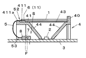
以下、本発明の実施例を添付図面を用いて説明する。図1は本発明の第1の実施例による表示装置の正面図、図2は図1のA−A線に沿った断面図、図3は図1のB−B線に沿った断面図、図4は図1のC−C線に沿った断面図、図5は接続部を図2中、矢印D方向から見た場合の要部正面図、図6は図3の矢印E領域の拡大断面図、図7は同上実施例における表示装置の組み付けを説明する要部分解断面図である。
【0023】
図1〜図4において表示装置は、表示素子1と、この表示素子1を背後から照明する光源2と、この光源2を保持すると共に表示素子1と導通接続される回路基板3と、この回路基板3上に表示素子1を支持するケース4と、表示素子1と回路基板3とを導通接続する可撓性回路基板5とで構成されている。
【0024】
表示素子1は、例えば一対のガラス基板間に液晶分子を封入した液晶パネルからなり、その端部には可撓性回路基板5と導通接続される複数の電極端子11(特に図1参照)を備えている。
【0025】
光源2は複数個の発光ダイオードからなり、ケース4の内部で表示素子1の長手方向に沿うように略等間隔で一列に配置されている(図4参照)。
【0026】
回路基板3は、ガラスエポキシ系材料からなる硬質の回路基板で、その所定箇所には可撓性回路基板5を介して各電極端子11に導通接続され、表示素子1に駆動信号を供給する複数の回路パターン31(図5参照)を有している。
【0027】
ケース4は、例えば白色系の合成樹脂にて略箱形に形成され、表示素子1を取り巻く周壁40と、表示素子1を支持する受壁41と、光源に対応する第1の開口部42と、表示素子1に対応する第2の開口部43と、これら開口部42,43間に位置する反射壁44とを有している。
【0028】
周壁40には、回路基板3側に延長し、先端部に回路基板3に係合する係合部が設けられたフック部401(図4参照)が形成され、このフック部401が回路基板3に係合することによりケース4を回路基板3に装着できるようになっている。また周壁40には、図1に示すように表示素子1の一対の角部前方側を保持する保持部402と、これら保持部402の反対側に位置して表示素子1の前方側に係合する係合フック部403とが形成され、表示素子1の一辺側角部を保持部402の背後に挿入した後に表示素子1を受部41側に押圧することにより表示素子1の他方側一辺が係合フック部403に係合し、これにより受部41に表示素子1を載置した状態でケース3に支持するようにしている。
【0029】
受壁41には、可撓性回路基板5に沿って外側に延長する延長壁411が形成され、この延長壁411の先端部に可撓性回路基板5と当接する突条部411a(図2、図3参照)が形成され、この突条部411aに可撓性回路基板5を当接させつつ回路基板3側に迂回させる構成となっている。この突条部411aは、可撓性回路基板5を迂回させて引き回す際の基点部となるもので、その頂部の突出寸法は、この部分を介して引き回される可撓性回路基板5部分と、後述する導通接続部(可撓性回路基板5と表示素子1の電極端子11との接続部分)を形成する可撓性回路基板5部分とが略同じ高さになるように設定されており、これにより前記導通接続部に過度な応力が加わることを防止している。また可撓性回路基板5の引き回し側となる受壁41部分には、回路基板3に向けて延長する一対の延長部412が延長壁411を挟むように、互いに間隔を空けて形成されている。これら延長部412の端部側には、回路基板3の板面に沿って延長する壁部(第1の規制部)413が形成され、この壁部413は、可撓性回路基板5を回路基板5側に押圧してその板面に沿わせることにより、可撓性回路基板5の浮き上がり方向(例えば図3中、垂直方向)移動を規制するものである。この壁部413には、回路基板3側に突出し、可撓性回路基板5と回路基板3の双方に形成される後述する各孔部に挿通される突出部(第2の規制部)414が形成され、この突出部414は、回路基板3の板面に対する可撓性回路基板5の板面方向(例えば図3中、水平方向)移動を規制するもので、壁部413と併せて突出部414を採用することで、可撓性回路基板5を図3中、垂直方向並びに水平方向に位置規制する規制部を構成している。
【0030】
反射壁44は、第1の開口部42の周囲から第2の開口部43に向けて次第に末広がり状に傾斜して延び、受壁41に連続している。そして、その内壁面により光源からの光を表示素子1に反射する照明室を形成しており、一方、反射壁44の外壁面は、これに対応する回路基板3の基板面との間で、照明には関与しない余剰部(余剰スペース)Sを形成している。
【0031】
可撓性回路基板5は、FPC、ヒートシールフィルム、平型導電性フィルム等と称されるもので、図1,図2及び図5に示すように、表示素子1の電極端子11及び回路基板3の回路パターン31に対応する複数の導電路51を有し、表示素子1側の端部52がその電極端子11に導通接続され、これにより導通接続部6が形成されると共に、回路基板3側の端部53がその回路パターン31に導通接続され、これにより接続部7が形成される。また端部53には、図5に示すように導電路51の列を挟むように孔部54が形成され、この孔部54と、この孔部54に対応して回路基板3位置に形成された孔部32(図6参照)との双方にケース4の突出部414を挿入することにより、端部53が回路基板3に対して位置規制されるようになっている。
なお可撓性回路基板5は、図示しない合成樹脂からなるベースフィルム上に複数本の導電路51を形成すると共に導電路51が形成された前記ベースフィルム上に同じく合成樹脂からなる保護フィルムを接合してなり、表示素子1の電極端子11に導通接続される箇所及び回路基板3の回路パターン31に導通接続される箇所は、前記保護フィルムが除去されて導電路51が露出しており、前記保護フィルムから露出した導電路51が電極端子11と回路パターン31の双方に接続されるものである。
【0032】
端部53と回路基板3(回路パターン31)との接続は、予め回路パターン31の所要部分に半田層(導電性物質)を形成した回路基板3上に、可撓性回路基板5の端部53を当接させて導電路51を回路パターン31に位置合わせし、可撓性回路基板5上から熱を加えることで前記半田層を溶融させて回路パターン31と導電路51とを半田付けし、これにより両者の所要部(図2中、括弧にて示す領域Fまたは図5中、一点鎖線で示す領域F参照)に半田接合による接続部7が形成される。なお導通接続部6も接続部7と同様、適宜導電性物質(例えばUV硬化型導電膜)を介して導電路51と電極端子11を接続することにより形成されている。
【0033】
この際、接続部7は、図2に示すように、ケース4と回路基板3との間(表示素子1の平面視においてケース4外形の回路基板3上投影範囲内)、すなわちケース4の反射壁44と回路基板3とで形成される余剰部S内に位置する回路基板3の板面箇所に位置している。
【0034】
以下、図7に基づいて本実施例による表示装置の組み付けについて説明する。まず、予め端部52が表示素子1の電極端子11に導通接続された可撓性回路基板5のもう一方の端部53(導電路51)を、回路基板3(回路パターン31)に前述の通り半田付けする。この際、両者の半田付けは、各孔部54,32に図示しない位置決め治具を挿入することにより端部53(導電部51)と回路基板3(回路パターン31)とを位置合わせした状態で行われ、半田付け完了後に前記位置決め治具が除去される。
次に端部53の前方より回路基板3上にケース4を配置し、フック部401(図4参照)を通じて回路基板3にケース4を装着する。この際、端部53はケース4の壁部413により回路基板3側に押圧されて浮き上がりが抑制されると共に、ケースの突出部414が各孔部54,32に挿入されることにより、板面方向への移動が規制され、これにより接続部7に対して応力が加わりにくい構造となる。
【0035】
次に保持部402と係合フック部403(図1参照)とを通じて表示素子1をケース4に装着し、組み付けが完了する。
【0036】
以上のように本実施例では、液晶パネルからなる表示素子1と、この表示素子1を背後から照明する光源2と、この光源2を保持すると共に表示素子1と導通接続される回路基板3と、この回路基板3上に表示素子1を支持するケース4と、表示素子1と回路基板3とを導通接続する可撓性回路基板5とを備えており、ケース4と回路基板3との間に可撓性回路基板5と回路基板3との接続部7を設けたことにより、回路基板3上のスペースを節約してスペース効率を高めることができ、これにより回路基板3を小型化し、コスト上昇を抑えることができる。また回路基板3上のスペース効率を高めることで、装置全体の大型化を抑え、小型化を達成することができる。
【0037】
また本実施例では、ケース4が光源2に対応する第1の開口部42と、表示素子2に対応する第2の開口部43と、これら第1,第2の開口部42,43間に位置し光源2からの光を表示素子1側に反射する反射壁44を有し、この反射壁44の外壁面と回路基板3との間の余剰部Sで可撓性回路基板5と回路基板3とを接続することにより、余剰部Sを利用してスペース効率を高めることができ、大きなメリットを得ることができる。
【0038】
また本実施例では、壁部(第1の規制部)413と突出部(第2の規制部)414とで可撓性回路基板5の端部53を位置規制したことにより、例えば組み付け作業に伴う機械的ストレス等の応力が接続部7に加わるのを抑制でき、接続信頼性を高めることができる。また本実施例では第1の規制部(壁部413)と第2の規制部(突出部414)とを延長部412を通じて集中的に設けたが、第1の規制部(壁部413)と第2の規制部(突出部414)とは、ケース4の適所に分散配置もしくは分離配置することも可能である。
【0039】
図8は本発明の第2の実施例を示す断面図であり、本実施例では可撓性回路基板5の端部53を回路基板3に設けたコネクタ8を介して接続し、接続部7を設けたものであり、かかる実施例によっても前記第1の実施例と同様、スペース効率を高めることができる。
【0040】
図9,図10は本発明の第3の実施例を示すもので、図9はケース装着前の要部断面図、図10はケース装着後の断面図であり、本実施例では、規制部を構成する壁部413と突出部414の近傍となる延長部412に部分的に薄肉となるヒンジ部Hを設け、このヒンジ部Hを基点としてケース4を回転装着する例を示している。すなわち、図9に示すように、予め表示素子1と可撓性回路基板5とを保持したケース4を、回路基板3上に縦置きし、ケースの壁部413と突出部414とで可撓性回路基板5の端部53を回路基板3に位置規制した状態で、可撓性回路基板5の端部53を回路基板3に半田付けして接続部7を設け、その後、薄肉ヒンジHを基点としてケース4を回転させ、図10に示すようにケース4を回路基板3に装着したものであり、かかる構成により、前記第1,第2の実施例と同様の効果を期待できる他、ケース4に表示素子1及び可撓性回路基板5を保持した状態で回路基板3に組み付けることができ、組み付け作業性を向上させることができる。しかも前記第1の実施例と比較した場合、その組み付け時において、接続部7に剥離方向(回路基板3と可撓性回路基板5との重ね方向)の応力が加わるのを抑制でき、接続部7の破損を予防することができる。
【0041】
また本実施例では、図示しないが、少なくともヒンジ部Hとは反対側となるケース4位置に、前記第1の実施例と同様なフック部(401)を設け、ヒンジ部Hを基点としたケース4の回転に応じて、フック部が回路基板3に係合するよう構成してもよく、このように構成することで、組み付けが更に容易となり、生産効率を高めることができる。
【0042】
図11〜図14は、本発明の第4の実施例を示すもので、図11は、本発明の第4の実施例による表示装置の正面図、図12は図11のG−G線に沿った断面図、図13及び図14は、同上実施例における表示装置の組み付けを示す概略図である。
【0043】
本実施例による表示装置は、前記第1〜第3の実施例と同様、可撓性回路基板5がケース4の一側部を経由して回路基板3側に引き回されており、ケース4の一側部側であって、可撓性回路基板5を挟むようにその両側に位置する側壁部404の回路基板3側端部には、回路基板3に係合する略「L」字状または「鍵」状の引っ掛け部405が形成され、またケース4の一側部とは反対側となる側壁部404であって、その回路基板3側端部には、弾性を有するフック部401が形成されている。
【0044】
そして、図13に示すように、予め表示素子1と可撓性回路基板5とを保持したケース4を、表示素子1が回路基板3と対面するように反対向きにし、この状態で可撓性回路基板5の端部53を回路基板3に半田付けして接続部7を設け、その後、図14に示すように、ケース4の引っ掛け部405を回路基板3に引っ掛けて、引っ掛け部405を基点としてケース4を回転させると、突出部414が回路基板3の孔部32に嵌合して可撓性回路基板5が位置規制され、さらにケース4を回転させると、フック部401が回路基板3に係合し、組み付けが完了するものである。
【0045】
これにより、前記第3の実施例と同様、ケース4に表示素子1及び可撓性回路基板5を保持した状態で回路基板3に組み付けることができ、組み付け作業性を向上させることができ、しかも組み付け時において、接続部7に剥離方向(回路基板3と可撓性回路基板5との重ね方向)の応力が働くのを抑制でき、接続部7の破損を予防することができる。また本例においても、少なくとも引っ掛け部405とは反対側となるケース4位置に、回路基板3に係合するフック部401を設け、引っ掛け部405を基点としたケース4の回転に応じて、フック部401が回路基板3に係合するよう構成したことにより、組み付けが更に容易となり、生産効率を高めることができる。
【0046】
なお前記第3,第4の実施例では、フック部(401)をケース4の一側部とは反対側となる側壁部(404)に設けたが、この部分以外にも形成することができる。
【0047】
【発明の効果】
以上詳述したように本発明は、表示素子と、この表示素子と導通接続される回路基板と、この回路基板上に前記表示素子を支持するケースと、前記表示素子と前記回路基板とを導通接続する可撓性回路基板とを備え、前記ケースと前記回路基板との間に前記可撓性回路基板と前記回路基板との接続部を設け、前記ケースに前記可撓性回路基板を前記回路基板に位置規制する規制部を形成し、前記規制部が少なくとも前記可撓性回路基板を前記回路基板の基板面に沿わせる第1の規制部と、前記回路基板の基板面に対する前記可撓性回路基板の板面方向移動を規制する第2の規制部とからなることにより、回路基板上のスペースを節約して小型化あるいはコスト低減を達成し得ることに加え、接続信頼性を向上させることが可能な表示装置を提供することができる。
【図面の簡単な説明】
【図1】本発明の第1の実施例による表示装置の正面図。
【図2】図1のA−A線に沿った断面図。
【図3】図1のB−B線に沿った断面図。
【図4】図1のC−C線に沿った断面図。
【図5】接続部を図2中、矢印D方向から見た場合の要部正面図。
【図6】図3の矢印E領域の拡大断面図。
【図7】同上実施例における表示装置の組み付けを説明する分解断面図。
【図8】本発明の第2の実施例を示す断面図。
【図9】本発明の第3の実施例による表示装置のケース装着前の要部断面図。
【図10】同上実施例における表示装置のケース装着後の断面図。
【図11】本発明の第4の実施例による表示装置の正面図。
【図12】図11のG−G線に沿った断面図。
【図13】同上実施例における表示装置の組み付けを示す概略図。
【図14】同上実施例における表示装置の組み付けを示す概略図。
【符号の説明】
1 表示素子
2 光源
3 回路基板
4 ケース
5 可撓性回路基板
6 導通接続部
7 接続部
8 コネクタ
11 電極端子
31 回路パターン
32,54 孔部
40 周壁
41 受壁
42 第1の開口部
43 第2の開口部
44 反射壁
51 導電路
52,53 端部
401 フック部
402 保持部
403 係合フック部
404 側壁部
405 引っ掛け部
411 延長壁
411a 突条部
412 延長部
413 壁部(第1の規制部)
414 突出部(第2の規制部)
S 余剰部(余剰スペース)
H ヒンジ部[0001]
BACKGROUND OF THE INVENTION
The present invention relates to a display device mounted on various devices, and more particularly to a display device including a display element that is backlit by a light source.
[0002]
[Prior art]
Conventionally, display devices using, for example, a liquid crystal panel as a display element are widely known. In many of such display devices, a display element is supported on a circuit board through a case called a light box, and the display element is backlit by a light source mounted on the circuit board. In addition, the display element and the circuit board are electrically connected to electrode terminals provided on the display element and a circuit pattern provided on the circuit board by a connecting member as appropriate, and supply a drive signal to the display element through the circuit board to display the display element and the circuit board. A predetermined display is performed on the element.
[0003]
As a connection member between the display element and the circuit board, for example, as shown in Japanese Patent Laid-Open No. 10-177155, a plurality of lead frames are used, and as shown in Japanese Patent Laid-Open No. 11-305202, for example. Some use rubber connectors (conductive rubber). These are practical when the pitch interval between the electrode terminals is relatively wide or when the number of electrode terminals is small, but for example, a display element that requires high resolution has a large number of electrode terminals and the pitch interval is large. Not suitable for narrow cases. Further, for example, as shown in Japanese Utility Model Laid-Open No. 5-47920, one using a flexible circuit board (FPC or flexible circuit board) is also known, and one using a flexible circuit board is an electrode. Even when the terminals have a very small pitch, the connection is easy, and there is an advantage that the display element can be reduced in size and resolution.
[0004]
[Problems to be solved by the invention]
However, in the case of using a flexible circuit board typified by Japanese Utility Model Laid-Open No. 5-47920, the connection portion between the flexible circuit board and the circuit board (hard circuit board) supports the display element. Since it is located on the outer side, a connection space is required on the circuit board located outside the case, and accordingly, the circuit board becomes larger and costs increase. In addition, since a connection space is required on the outside of the case, there is a problem that the entire apparatus including the circuit board is enlarged.In addition, for example, excessive stress such as mechanical stress may be applied to the connection portion between the flexible circuit board and the circuit board during the assembling work.
[0005]
The present invention has been made in view of this point, and the main object of the present invention is to save space on the circuit board and achieve miniaturization or cost reduction.In addition, connection reliability can be improvedA display device is provided.
[0006]
[Means for Solving the Problems]
In order to achieve the above object, the present invention provides a display element, a circuit board electrically connected to the display element, a case for supporting the display element on the circuit board, the display element and the circuit board. A flexible circuit board that is conductively connected, and a connection portion between the flexible circuit board and the circuit board is provided between the case and the circuit board.A first restricting portion that forms a restricting portion for restricting the position of the flexible circuit board on the circuit board in the case, and the restricting portion causes at least the flexible circuit board to run along a substrate surface of the circuit board. And a second restricting portion for restricting movement of the flexible circuit board in the plate surface direction with respect to the board surface of the circuit board.It is characterized by that.
[0007]
According to the present invention, a light source that illuminates the display element is provided on the circuit board, and the case has a first opening corresponding to the light source, a second opening corresponding to the display element, and these A reflection wall that is positioned between the first and second openings and reflects light from the light source toward the display element, and the connection portion is provided between the outer wall surface of the reflection wall and the circuit board. It is provided.
[0008]
Further, the present invention is characterized in that the connection portion is formed by joining the flexible circuit board and the circuit board via a predetermined conductive material.
[0009]
Further, the present invention is characterized in that the connecting portion is formed by connecting the flexible circuit board and the circuit board via a connector.
[0012]
Further, the present invention is characterized in that a hinge portion is formed in the vicinity of the restricting portion, and the case is rotatably provided with the hinge portion as a base point.
[0013]
Further, the present invention is characterized in that a hook portion that engages with the circuit board is provided at least in a case position opposite to the hinge portion.
[0014]
According to the present invention, the flexible circuit board extends to the circuit board side via one side of the case, and a hook portion that engages with the circuit board is formed on one side of the case. The case is provided so that the case can be rotatably mounted with the hook portion as a base point.
[0015]
Further, the present invention is characterized in that a hook portion that engages with the circuit board is provided at least in a case position opposite to the hook portion.
[0016]
DETAILED DESCRIPTION OF THE INVENTION
A display device according to the present invention includes, for example, a light-receiving display element formed of a liquid crystal panel, a light source formed of, for example, a light-emitting diode that illuminates the display element from the back, and glass, for example, that holds the light source and is electrically connected to the display element A case comprising: a hard circuit board made of an epoxy-based material; a case made of synthetic resin that supports the display element on the circuit board; and a flexible circuit board that electrically connects the display element and the circuit board. A connection portion between the flexible circuit board and the circuit board is provided between the circuit board and the circuit board. Thus, by providing the connection part behind the case, the space on the circuit board can be saved and the space efficiency can be improved, the circuit board can be downsized, and the cost increase can be suppressed. Further, by increasing the space efficiency on the circuit board, it is possible to suppress an increase in the size of the entire apparatus and achieve a reduction in size. Note that at least a part of the connecting portion may be located between the case and the circuit board (within the projection range on the circuit board of the case outer shape in a plan view of the display element). The larger the connection area between the two, the more advantageous the space saving. Ideally, the entire connection area should be positioned between the case or the display element and the circuit board. In addition to a light receiving display element such as a liquid crystal panel, a self-luminous display element such as an EL panel or a fluorescent display tube (VFD) can also be applied as the display element. Needless to say, when a display element is used, a light source is unnecessary.
[0017]
The case is located between the first opening corresponding to the light source, the second opening corresponding to the display element, and the first and second openings, and reflects light from the light source toward the display element. In the case of having a reflection wall, by providing a connection portion between the outer wall surface of the reflection wall and the circuit board, the extra space between the outer wall surface of the reflection wall and the corresponding substrate surface of the circuit board can be flexibly provided. The circuit board can be connected to the circuit board, which has a great merit in improving the space efficiency. That is, the reflection wall that reflects light from the light source to the display element side usually extends from the periphery of the first opening portion to the second opening portion so as to be inclined or curved, and its inner wall surface An illumination room for illuminating is formed, but the outer wall surface of the reflecting wall forms a surplus space that does not participate in illumination with the corresponding substrate surface of the circuit board, and a connecting portion is provided in this surplus space. If the space on the circuit board can be saved by positioning, there is a great advantage in space efficiency.
[0018]
Further, when connecting the flexible circuit board and the circuit board, a connecting portion is formed by bonding the two through a predetermined conductive material, for example, solder, anisotropic conductive film, UV curable conductive film. Alternatively, the connecting portion may be formed by connecting the two via a dedicated connector such as a connector.
[0019]
Further, if a restricting portion for restricting the position of the flexible circuit board on the circuit board is formed in the case, it is possible to suppress an excessive stress from being applied to the connecting portion and to improve the connection reliability. As such a positioning portion, a first restricting portion that causes the flexible circuit board to run along the substrate surface on the circuit board side, and a first restricting portion that moves the flexible circuit board relative to the substrate surface of the circuit board. When formed with the two restricting portions, the first restricting portion suppresses the floating of the flexible circuit board from the circuit board, and prevents the stress applied to the connecting portion due to the lifting or reduces the stress itself. The second restricting portion suppresses the movement of the flexible circuit board in the plate surface direction, prevents the stress applied to the connection portion along with the movement in the plate surface direction or reduces the stress itself, and improves the connection reliability. Is advantageous.
[0020]
When the case is made of, for example, synthetic resin, a thin hinge portion is provided in the vicinity of the restricting portion, and the case can be rotatably mounted with the hinge portion as a base, thereby holding the display element and the flexible circuit board in the case. In this state, it can be assembled to the circuit board, and the assembling workability can be improved. Moreover, it is difficult to apply the stress in the peeling direction to the connecting portion at the time of assembling, and damage to the connecting portion can be prevented. Further, in this case, a hook portion that engages with the circuit board is provided at least on the case position opposite to the hinge portion, and the hook portion engages with the circuit board according to the rotation of the case with the hinge portion as a base point. If comprised in this way, an assembly | attachment becomes still easier and production efficiency can be improved.
[0021]
In addition, when the flexible circuit board is routed to the circuit board side via one side portion of the case, a hook portion that engages with the circuit board is provided on one side portion of the case, and the hook portion serves as a base point. The case may be provided so as to be rotationally mountable. By configuring in this way, the display element and the flexible circuit board can be assembled to the circuit board while being held in the case, which improves the assembling workability. In addition, during assembly, it is difficult to apply a stress in the peeling direction to the connecting portion, and damage to the connecting portion can be prevented. Further, in this case, a hook portion that engages with the circuit board is provided at least on the case position opposite to the hook portion, and the hook portion engages with the circuit board according to the rotation of the case with the hook portion as a base point. If comprised in this way, an assembly | attachment becomes still easier and production efficiency can be improved.
[0022]
【Example】
Embodiments of the present invention will be described below with reference to the accompanying drawings. 1 is a front view of a display device according to a first embodiment of the present invention, FIG. 2 is a sectional view taken along line AA in FIG. 1, and FIG. 3 is a sectional view taken along line BB in FIG. 4 is a cross-sectional view taken along the line C-C in FIG. 1, FIG. 5 is a front view of the main part when the connecting portion is viewed from the direction of arrow D in FIG. 2, and FIG. Sectional drawing and FIG. 7 are principal part exploded sectional drawings explaining the assembly | attachment of the display apparatus in an Example same as the above.
[0023]
1 to 4, the display device includes a
[0024]
The
[0025]
The
[0026]
The
[0027]
The
[0028]
The
[0029]
An
[0030]
The
[0031]
The
The
[0032]
The
[0033]
At this time, as shown in FIG. 2, the connecting
[0034]
Hereinafter, the assembly of the display device according to the present embodiment will be described with reference to FIG. First, the other end 53 (conductive path 51) of the
Next, the
[0035]
Next, the
[0036]
As described above, in this embodiment, the
[0037]
In this embodiment, the
[0038]
Further, in this embodiment, the position of the
[0039]
FIG. 8 is a cross-sectional view showing a second embodiment of the present invention. In this embodiment, the
[0040]
FIGS. 9 and 10 show a third embodiment of the present invention. FIG. 9 is a cross-sectional view of the main part before mounting the case, and FIG. 10 is a cross-sectional view after mounting the case. In this example, a hinge portion H that is partially thin is provided on the
[0041]
Further, in this embodiment, although not shown in the drawings, a case where the same hook portion (401) as that in the first embodiment is provided at least in the
[0042]
FIGS. 11 to 14 show a fourth embodiment of the present invention, FIG. 11 is a front view of a display device according to the fourth embodiment of the present invention, and FIG. 12 is taken along line GG in FIG. FIG. 13 and FIG. 14 are schematic views showing the assembly of the display device according to the same embodiment.
[0043]
In the display device according to this embodiment, the
[0044]
Then, as shown in FIG. 13, the
[0045]
Thus, as in the third embodiment, the
[0046]
In the third and fourth embodiments, the hook portion (401) is provided on the side wall portion (404) opposite to one side portion of the
[0047]
【The invention's effect】
As described above in detail, the present invention provides a display element, a circuit board electrically connected to the display element, a case for supporting the display element on the circuit board, and the display element and the circuit board. A flexible circuit board to be connected, and a connecting portion between the flexible circuit board and the circuit board is provided between the case and the circuit board.A first restricting portion that forms a restricting portion for restricting the position of the flexible circuit board on the circuit board in the case, and the restricting portion causes at least the flexible circuit board to run along a substrate surface of the circuit board. And a second restricting portion for restricting movement of the flexible circuit board in the plate surface direction with respect to the board surface of the circuit board.Can save space on the circuit board and achieve downsizing or cost reductionIn addition, connection reliability can be improvedA display device can be provided.
[Brief description of the drawings]
FIG. 1 is a front view of a display device according to a first embodiment of the present invention.
2 is a cross-sectional view taken along line AA in FIG.
3 is a cross-sectional view taken along line BB in FIG.
4 is a cross-sectional view taken along the line CC of FIG.
5 is a front view of the main part when the connection part is viewed from the direction of arrow D in FIG. 2. FIG.
6 is an enlarged cross-sectional view of a region indicated by an arrow E in FIG.
FIG. 7 is an exploded cross-sectional view for explaining assembly of the display device in the embodiment.
FIG. 8 is a sectional view showing a second embodiment of the present invention.
FIG. 9 is a cross-sectional view of a main part of a display device according to a third embodiment of the present invention before mounting a case.
FIG. 10 is a cross-sectional view of the display device according to the embodiment after the case is mounted.
FIG. 11 is a front view of a display device according to a fourth embodiment of the present invention.
12 is a sectional view taken along line GG in FIG.
FIG. 13 is a schematic view showing assembly of the display device in the embodiment.
FIG. 14 is a schematic diagram showing assembly of the display device in the embodiment.
[Explanation of symbols]
1 Display element
2 Light source
3 Circuit board
4 cases
5 Flexible circuit board
6 Conductive connection
7 connections
8 Connector
11 Electrode terminal
31 Circuit pattern
32, 54 hole
40 wall
41 Receiving wall
42 First opening
43 Second opening
44 Reflecting wall
51 Conductive path
52,53 end
401 hook
402 holding part
403 engagement hook
404 Side wall
405 hook
411 Extension wall
411a ridge
412 Extension
413 Wall (first regulating part)
414 Projection (second regulating part)
S Surplus part (surplus space)
H Hinge part
Claims (8)
この表示素子と導通接続される回路基板と、
この回路基板上に前記表示素子を支持するケースと、
前記表示素子と前記回路基板とを導通接続する可撓性回路基板とを備え、
前記ケースと前記回路基板との間に前記可撓性回路基板と前記回路基板との接続部を設け、
前記ケースに前記可撓性回路基板を前記回路基板に位置規制する規制部を形成し、
前記規制部が少なくとも前記可撓性回路基板を前記回路基板の基板面に沿わせる第1の規制部と、前記回路基板の基板面に対する前記可撓性回路基板の板面方向移動を規制する第2の規制部とからなることを特徴とする表示装置。A display element;
A circuit board electrically connected to the display element;
A case for supporting the display element on the circuit board;
A flexible circuit board that conductively connects the display element and the circuit board;
A connecting portion between the flexible circuit board and the circuit board is provided between the case and the circuit board ,
Forming a restricting portion for restricting the position of the flexible circuit board on the circuit board in the case;
The restricting portion restricts movement of the flexible circuit board in the plate surface direction relative to the substrate surface of the circuit board, and a first restricting portion that causes at least the flexible circuit board to run along the board surface of the circuit board. A display device comprising two restriction portions .
前記ケースが前記光源に対応する第1の開口部と、
前記表示素子に対応する第2の開口部と、
これら第1,第2の開口部間に位置し前記光源からの光を前記表示素子側に反射する反射壁とを有し、この反射壁の外壁面と前記回路基板との間に前記接続部を設けたことを特徴とする請求項1記載の表示装置。A light source for illuminating the display element on the circuit board;
A first opening corresponding to the light source of the case;
A second opening corresponding to the display element;
A reflection wall that is positioned between the first and second openings and reflects light from the light source toward the display element; and the connection portion between the outer wall surface of the reflection wall and the circuit board. The display device according to claim 1, further comprising:
Priority Applications (1)
| Application Number | Priority Date | Filing Date | Title |
|---|---|---|---|
| JP2001075360A JP3747458B2 (en) | 2001-01-31 | 2001-03-16 | Display device |
Applications Claiming Priority (3)
| Application Number | Priority Date | Filing Date | Title |
|---|---|---|---|
| JP2001-22932 | 2001-01-31 | ||
| JP2001022932 | 2001-01-31 | ||
| JP2001075360A JP3747458B2 (en) | 2001-01-31 | 2001-03-16 | Display device |
Publications (2)
| Publication Number | Publication Date |
|---|---|
| JP2002304131A JP2002304131A (en) | 2002-10-18 |
| JP3747458B2 true JP3747458B2 (en) | 2006-02-22 |
Family
ID=26608602
Family Applications (1)
| Application Number | Title | Priority Date | Filing Date |
|---|---|---|---|
| JP2001075360A Expired - Fee Related JP3747458B2 (en) | 2001-01-31 | 2001-03-16 | Display device |
Country Status (1)
| Country | Link |
|---|---|
| JP (1) | JP3747458B2 (en) |
Families Citing this family (9)
| Publication number | Priority date | Publication date | Assignee | Title |
|---|---|---|---|---|
| JP4606174B2 (en) * | 2004-08-19 | 2011-01-05 | 矢崎総業株式会社 | Mounting structure of liquid crystal display device |
| JP4578902B2 (en) * | 2004-09-09 | 2010-11-10 | 矢崎総業株式会社 | Display device |
| JP4868569B2 (en) * | 2005-03-30 | 2012-02-01 | リズム時計工業株式会社 | Liquid crystal display |
| JP5903813B2 (en) * | 2011-09-15 | 2016-04-13 | ブラザー工業株式会社 | Liquid crystal display |
| JP5698690B2 (en) * | 2012-02-24 | 2015-04-08 | シャープ株式会社 | Display device and television receiver |
| JP6248500B2 (en) * | 2013-09-24 | 2017-12-20 | 日本精機株式会社 | Display device |
| JP6338873B2 (en) * | 2014-02-04 | 2018-06-06 | Hoya株式会社 | Protective cover set |
| KR102557654B1 (en) * | 2016-07-04 | 2023-07-19 | 엘지전자 주식회사 | Display device |
| JP2018091624A (en) * | 2018-03-16 | 2018-06-14 | 東芝ライフスタイル株式会社 | refrigerator |
-
2001
- 2001-03-16 JP JP2001075360A patent/JP3747458B2/en not_active Expired - Fee Related
Also Published As
| Publication number | Publication date |
|---|---|
| JP2002304131A (en) | 2002-10-18 |
Similar Documents
| Publication | Publication Date | Title |
|---|---|---|
| US8934068B2 (en) | Backlight assembly and method of assembling the same and liquid crystal display including backlight assembly | |
| KR100936099B1 (en) | Liquid crystal display device having flexible substrates | |
| JP4226796B2 (en) | Liquid crystal display | |
| US8305518B2 (en) | LED backlight and liquid crystal display device | |
| US7891858B2 (en) | Display | |
| EP1903376A1 (en) | Liquid crystal display device and portable display apparatus using the same | |
| JP2008034386A (en) | Integrated lamp socket, backlight assembly provided with the socket and display device | |
| JP3747458B2 (en) | Display device | |
| JP2008084790A (en) | Surface light source device and image display module employing it | |
| JP2007121594A (en) | Picture display module | |
| JP2007212931A (en) | Display device | |
| US8337046B2 (en) | Luminous element for backlight unit | |
| JP2001350422A (en) | Display device for electronic apparatus | |
| JP5678298B2 (en) | Light source unit | |
| JP2002229475A (en) | Display device | |
| JP3792574B2 (en) | Backlight structure of liquid crystal display device | |
| JP2002296569A (en) | Lcd module and portable terminal equipment | |
| KR20070054353A (en) | Display device | |
| JPH07218913A (en) | Liquid crystal display device with back light | |
| JP3876614B2 (en) | LCD module | |
| JP4060634B2 (en) | Liquid crystal display | |
| JP2589193Y2 (en) | Display device | |
| JPH1164832A (en) | Liquid crystal display device | |
| JP2006245272A (en) | Light-emitting diode device, planar light source unit, and meter | |
| KR19980041095A (en) | LED panel for LCD module |
Legal Events
| Date | Code | Title | Description |
|---|---|---|---|
| A977 | Report on retrieval |
Free format text: JAPANESE INTERMEDIATE CODE: A971007 Effective date: 20040729 |
|
| A131 | Notification of reasons for refusal |
Free format text: JAPANESE INTERMEDIATE CODE: A131 Effective date: 20040820 |
|
| A521 | Written amendment |
Free format text: JAPANESE INTERMEDIATE CODE: A523 Effective date: 20041013 |
|
| TRDD | Decision of grant or rejection written | ||
| A01 | Written decision to grant a patent or to grant a registration (utility model) |
Free format text: JAPANESE INTERMEDIATE CODE: A01 Effective date: 20051107 |
|
| A61 | First payment of annual fees (during grant procedure) |
Free format text: JAPANESE INTERMEDIATE CODE: A61 Effective date: 20051120 |
|
| R150 | Certificate of patent or registration of utility model |
Free format text: JAPANESE INTERMEDIATE CODE: R150 |
|
| FPAY | Renewal fee payment (event date is renewal date of database) |
Free format text: PAYMENT UNTIL: 20101209 Year of fee payment: 5 |
|
| LAPS | Cancellation because of no payment of annual fees |