JP3746050B2 - Optical compensation film, polarizing plate with optical compensation layer using the same, and liquid crystal display device using the same - Google Patents
Optical compensation film, polarizing plate with optical compensation layer using the same, and liquid crystal display device using the same Download PDFInfo
- Publication number
- JP3746050B2 JP3746050B2 JP2003345875A JP2003345875A JP3746050B2 JP 3746050 B2 JP3746050 B2 JP 3746050B2 JP 2003345875 A JP2003345875 A JP 2003345875A JP 2003345875 A JP2003345875 A JP 2003345875A JP 3746050 B2 JP3746050 B2 JP 3746050B2
- Authority
- JP
- Japan
- Prior art keywords
- group
- liquid crystal
- optical compensation
- display device
- crystal display
- Prior art date
- Legal status (The legal status is an assumption and is not a legal conclusion. Google has not performed a legal analysis and makes no representation as to the accuracy of the status listed.)
- Expired - Fee Related
Links
- 0 Cc(cc1)cc(C)c1C(C(N*)=CC(C)=C1)=C*1NC Chemical compound Cc(cc1)cc(C)c1C(C(N*)=CC(C)=C1)=C*1NC 0.000 description 2
Images


Description
本発明は、光学補償フィルム、それを用いた光学補償層付偏光板、および、それらを用いた液晶表示装置に関する。 The present invention relates to an optical compensation film, a polarizing plate with an optical compensation layer using the same, and a liquid crystal display device using them.
現在、パソコンモニターやTV等の画像表示装置において、垂直配向(VA)モードのTFT駆動式液晶表示装置の利用が増加している。そして、このVAモードの特徴は、黒表示(電荷印加時)における上下左右対称の視角特性にあるため、斜視方向からのコントラスト低下や、斜めから見た場合の黒表示部におけるカラーシフトが問題となっている。この表示品位の角度依存性を改善するために、2枚の偏光板の間に、さらに、例えば、A-プレートとC-プレートとの積層位相差板等の位相差板が配置されている。前記A−プレートには、例えば、ノルボルネン系の熱可塑性高分子等が使用され、前記C-プレートには、コレステリック液晶等が使用されている。しかしながら、これらの位相差板は、位相差特性が不十分であったために、さらに、同一種類の位相差板や正の一軸性位相差板を積層する等して複数枚を組合せなければ十分な光学特性を得ることができず、このことは、液晶表示装置の薄型化や低コスト化において大きな課題である。 Currently, the use of a vertical alignment (VA) mode TFT-driven liquid crystal display device is increasing in image display devices such as personal computer monitors and TVs. The characteristic of this VA mode is the vertical and left-right symmetric viewing angle characteristics during black display (when a charge is applied), and therefore there are problems such as a decrease in contrast from the perspective direction and a color shift in the black display portion when viewed obliquely. It has become. In order to improve the angle dependency of the display quality, a retardation plate such as a laminated retardation plate of an A-plate and a C-plate is further disposed between the two polarizing plates. For example, a norbornene-based thermoplastic polymer is used for the A-plate, and a cholesteric liquid crystal or the like is used for the C-plate. However, these retardation plates have insufficient phase difference characteristics, so that it is sufficient if a plurality of plates are not combined by stacking the same type of retardation plates or positive uniaxial retardation plates. Optical characteristics cannot be obtained, which is a big problem in reducing the thickness and cost of liquid crystal display devices.
そこで近年、基材上に塗工し乾燥させることにより負の一軸性を示すポリイミド等のポリマー材料を使用して、光学補償用二軸性位相差板を作製する方法が開示されている(例えば、特許文献1参照)。前記ポリイミド製フィルムの屈折率分布と、前記フィルムをさらに延伸することによる屈折率分布の変化については、延伸前後の特性として、nTE1=nTE2≠nTM、および、nTE1≠nTE2≠nTM という光学特性がそれぞれ開示されている(特許文献2参照)。また、屈折率分布の制御が容易であり、均一性の高い二軸性の光学フィルムを製造する方法が開示されている(特許文献3参照)。しかしながら、現在では、さらに優れた光学特性を示す二軸性位相差板が求められている。
そこで、本発明は、液晶表示装置の斜視方向におけるコントラスト低下や、斜めから見た場合の黒表示部におけるカラーシフト等を改善するための、優れた光学特性を有する光学補償フィルムの提供を目的とする。 Therefore, the present invention aims to provide an optical compensation film having excellent optical characteristics for improving contrast reduction in a perspective direction of a liquid crystal display device, color shift in a black display portion when viewed from an oblique direction, and the like. To do.
前記目的を達成するために、本発明の光学補償フィルムは、VA(垂直配向)モード液晶表示装置用光学補償フィルムであって、厚みが、2〜10μmの範囲であり、ポリイミド、ポリエーテルケトン、ポリアミドイミドおよびポリエステルイミドからなる群から選択される少なくとも一種のポリマー材料を含む形成材料から形成され、下記条件(I)から(III)の全てを満たす。 In order to achieve the above object, the optical compensation film of the present invention is an optical compensation film for a VA (vertical alignment) mode liquid crystal display device having a thickness in the range of 2 to 10 μm, polyimide, polyetherketone, It is formed from a forming material containing at least one polymer material selected from the group consisting of polyamideimide and polyesterimide, and satisfies all of the following conditions (I) to (III) .
3<(nx−nz)/(nx−ny)<6 (I)
100nm≦(nx−nz)d≦400nm (II)
nx>ny>nz (III)
上記条件(I)から(III)中、nx、nyおよびnzは、それぞれ、前記光学補償フィルムにおけるX軸、Y軸およびZ軸方向の屈折率を示し、前記X軸とは、前記光学補償フィルムの面内において最大の屈折率を示す軸方向であり、Y軸は、前記面内において前記X軸に対して垂直な軸方向であり、Z軸は、前記X軸およびY軸に垂直な厚み方向を示す。また、上記条件(II)中、(nx−nz)dは、厚み方向の位相差値(Rth)であって、dは、前記光学補償フィルムの厚みを示す。なお、前記条件(III)からわかるように、本発明の光学補償フィルムは、nx>ny>nzを示す二軸性の複屈折フィルムである。
3 <(nx-nz) / (nx-ny) < 6 (I)
100 nm ≦ (nx−nz) d ≦ 400 nm (II)
nx>ny> nz (III)
In the above conditions (I) to (III) , nx, ny, and nz respectively indicate refractive indexes in the X-axis, Y-axis, and Z-axis directions of the optical compensation film, and the X-axis is the optical compensation film In which the Y axis is an axial direction perpendicular to the X axis and the Z axis is a thickness perpendicular to the X axis and the Y axis. Indicates direction. In the above condition (II), (nx−nz) d is a retardation value (Rth) in the thickness direction, and d indicates the thickness of the optical compensation film. As can be seen from the condition (III) , the optical compensation film of the present invention is a biaxial birefringent film exhibiting nx>ny> nz.
本発明者らは、VAモード液晶表示装置の視角特性の改善には、前記光学補償フィルムにおける下記式で表される面内位相差(Δnd)と厚み方向の位相差(Rth)との関係が非常に重要であるとの知見を得て、(nx−nz)/(nx−ny)で表される前記2つの位相差の関係を含む前記条件(I)から(III)の全てを満たせば、前記光学補償フィルムをVAモード液晶表示装置に使用した際に、その視野角特性を大幅に改善できることを見出し、本発明に到達した。具体的には、本発明の光学補償フィルムは、前記条件(I)から(III)の全てを満たす優れた光学特性を有するため、液晶表示装置に使用すれば、例えば、表示画面における斜視方向からのコントラスト向上や、斜めから見た場合の黒表示部におけるカラーシフトの改善等により、さらに広視野角化が実現できる。また、本発明の光学補償フィルムは、単独で前記条件(I)から(III)の全てを満たすため、一枚でも十分な光学補償能を発揮し、従来の積層位相差板に比べて薄型化も可能であり、前記液晶表示装置の低コスト化も実現できる。なお、下記式において、nx、ny、nyは、前述と同様であり、dは、光学補償フィルムの厚みを示す。
Δnd=(nx−ny)d
Rth=(nx−nz)d
In order to improve the viewing angle characteristics of the VA mode liquid crystal display device, the present inventors have found that the relationship between the in-plane retardation (Δnd) and the thickness direction retardation (Rth) of the optical compensation film represented by the following formula. If the knowledge that it is very important is obtained and all of the conditions (I) to (III) including the relationship between the two phase differences represented by (nx−nz) / (nx−ny) are satisfied, When the optical compensation film is used in a VA mode liquid crystal display device, it has been found that the viewing angle characteristics can be greatly improved, and the present invention has been achieved. Specifically, since the optical compensation film of the present invention has excellent optical characteristics that satisfy all of the above conditions (I) to (III), when used in a liquid crystal display device, for example, from a perspective direction on a display screen. The viewing angle can be further widened by improving the contrast and improving the color shift in the black display portion when viewed obliquely. In addition, the optical compensation film of the present invention alone satisfies all of the above conditions (I) to (III), so even a single sheet exhibits sufficient optical compensation capability, and is thinner than conventional laminated phase difference plates. In addition, the liquid crystal display device can be reduced in cost. In the following formula, nx, ny, and ny are the same as described above, and d indicates the thickness of the optical compensation film.
Δnd = (nx−ny) d
Rth = (nx−nz) d
本発明の光学補償フィルムは、他の位相差フィルムと組み合わせなくとも優れた光学特性を有する。このため、本発明の光学補償フィルムや光学補償層付偏光板を液晶表示装置に用いれば、1枚のみで液晶表示装置の斜視方向からのコントラスト低下や、斜めから見た場合の黒表示部におけるカラーシフト等を改善でき、その結果、表示品位の視野角依存性を改善できる。さらに、本発明の光学補償層は、薄型化が可能であるから、前記液晶表示装置の薄型化、低コスト化が可能となる。 The optical compensation film of the present invention has excellent optical properties without being combined with other retardation films. For this reason, if the optical compensation film or polarizing plate with an optical compensation layer of the present invention is used in a liquid crystal display device, the contrast of the liquid crystal display device from the perspective direction is reduced with only one sheet, or in the black display portion when viewed from an oblique direction. Color shift and the like can be improved, and as a result, the viewing angle dependency of display quality can be improved. Furthermore, since the optical compensation layer of the present invention can be thinned, the liquid crystal display device can be thinned and reduced in cost.
本発明の光学補償フィルムは、前述のように、(nx−nz)/(nx−ny)が、前記条件(I)を満たす。前記(nx−nz)/(nx−ny)が3より大きければ、本発明の光学補償フィルムをVAモード液晶表示装置に用いた場合に十分なコントラスト比が得られ、また、前記(nx−nz)/(nx−ny)が6未満であれば、従来のような負の一軸性フィルムを用いた場合に比べて視野角特性に優れる。 In the optical compensation film of the present invention, (nx−nz) / (nx−ny) satisfies the condition (I) as described above. When (nx−nz) / (nx−ny) is greater than 3, a sufficient contrast ratio can be obtained when the optical compensation film of the present invention is used in a VA mode liquid crystal display device, and the (nx−nz) ) / (Nx−ny) is less than 6 , it is excellent in viewing angle characteristics as compared with a conventional negative uniaxial film.
本発明の光学補償フィルムを用いる液晶表示装置の液晶セルがVAモードである場合、前記(nx−nz)/(nx−ny)は、前記条件(I)に代えて、下記条件(IV)を満たすことが特に好ましい。
3<(nx−nz)/(nx−ny)≦4.1 (IV)
When the liquid crystal cell of the liquid crystal display device using the optical compensation film of the present invention is in the VA mode, the above (nx−nz) / (nx−ny) satisfies the following condition (IV) instead of the condition (I). It is particularly preferable to satisfy it.
3 <(nx−nz) / (nx−ny) ≦ 4.1 (IV)
本発明の光学補償フィルムにおける屈折率nx、ny、およびnzの値は、用いるポリマー材料およびフィルム作製条件に依存してほぼ決まる。具体的には、前記条件(I)における(nx−nz)、すなわち厚み方向の複屈折率ΔNxzは、例えば、ポリマー主鎖の剛直性、直線性、対称性が高いほど、また、ポリマーの固有粘度が大きいほど(分子量が大きいほど)、大きくなる傾向にある。これに対して、前記条件(I)における(nx−ny)、すなわち面内方向の複屈折率ΔNxyは、例えば、フィルムの厚みが大きくなるほど、低下する傾向にある。 The values of the refractive indices nx, ny, and nz in the optical compensation film of the present invention are substantially determined depending on the polymer material used and the film production conditions. Specifically, (nx−nz) in the above condition (I), that is, the birefringence ΔNxz in the thickness direction, for example, the higher the rigidity, linearity, and symmetry of the polymer main chain, It tends to increase as the viscosity increases (the molecular weight increases). On the other hand, (nx−ny) in the condition (I), that is, the birefringence ΔNxy in the in-plane direction, tends to decrease as the thickness of the film increases, for example.
前記厚み方向の複屈折率ΔNxzは、前記面内方向の複屈折率ΔNxyとの関係で設定されるが、相対的に大きいことが好ましく、例えば、0.002以上である。前記ΔNxzが0.002以上あれば、従来のように厚み方向の位相差を得るために膜厚を厚くしたり、さらに他の位相差フィルムを積層する必要がなく、薄型化が実現できる。前記ΔNxzとしては、好ましくは0.005以上であり、0.01以上がより好ましく、さらにより好ましくは、0.02以上である。一方、前記面内方向の複屈折率ΔNxyは、例えば、0.0002以上0.1以下であることが好ましい。前記ΔNxyが0.0002以上ならば、本発明の光学補償フィルムは、負の二軸性複屈折フィルムとして十分に機能でき、0.1以下ならば、例えば、後述するように延伸によって本発明の光学補償フィルムを作製する場合に、前記フィルムに破断が生じにくい。 The birefringence ΔNxz in the thickness direction is set in relation to the birefringence ΔNxy in the in-plane direction, but is preferably relatively large, for example, 0.002 or more. If the ΔNxz is 0.002 or more, it is not necessary to increase the film thickness in order to obtain a retardation in the thickness direction as in the prior art, or to laminate another retardation film, and it is possible to reduce the thickness. The ΔNxz is preferably 0.005 or more, more preferably 0.01 or more, and even more preferably 0.02 or more. On the other hand, the birefringence ΔNxy in the in-plane direction is preferably 0.0002 or more and 0.1 or less, for example. If the above ΔNxy is 0.0002 or more, the optical compensation film of the present invention can sufficiently function as a negative biaxial birefringent film. When producing an optical compensation film, the film is less likely to break.
本発明の光学補償フィルムにおいて、厚み方向の位相差値Rthは、例えば、100nm以上400nm以下である。前記Rthが100nm以上であれば、光学素子として機能するに十分な位相差値であり、前記Rthが400nm以下であれば、例えば、使用するポリマーの塗布や乾燥時にムラができにくく、極めて均一なフィルムを得ることができる。前記Rthとしては、好ましくは、100nm以上300nm以下である。また、面内方向の位相差値Δndは、液晶表示装置の視野角特性の改善効果が大きくなることから、例えば、10nm以上990nm以下であって、好ましくは、20nm以上390nm以下である。 In the optical compensation film of the present invention, the thickness direction retardation value Rth is, for example, not less than 100 nm and not more than 400 nm. If the Rth is 100 nm or more, the retardation value is sufficient to function as an optical element. If the Rth is 400 nm or less, for example, it is difficult to cause unevenness when the polymer to be used is applied or dried, and is extremely uniform. A film can be obtained. The Rth is preferably 100 nm or more and 300 nm or less. The in-plane retardation value Δnd is, for example, 10 nm or more and 990 nm or less, and preferably 20 nm or more and 390 nm or less, because the effect of improving the viewing angle characteristics of the liquid crystal display device is increased.
本発明の光学補償フィルムは、前述のように液晶表示装置に使用した際に、コントラストに優れるという効果を奏する。具体的には、液晶画像表示装置の液晶セルと偏光板との間に配置された場合に、その表示画面の法線を基準として全方位に0〜80°の範囲で傾斜させた方向から測定したコントラスト比が10以上を示すことが好ましい。このコントラスト比の測定は、例えば、以下に示す方法で行うことができる。まず、本発明の光学補償フィルムを偏光板に積層して光学補償層付偏光板を作製し、これを液晶セルに実装する。なお、前記光学補償層付偏光板は、前記光学補償フィルムが液晶セルに対向するように実装し、前記液晶セルは、VAモードであることが好ましい。次に、この液晶表示装置に白画像および黒画像を表示させ、輝度計(商品名EzContrast160D、ELDI社製)により、XYZ表示系におけるY値、x値およびy値をそれぞれ測定する。コントラスト比は、白画像における前記Y値(Yw)と黒画像における前記Y値(Yb)とから、Yw/Ybとして求めることができる。 The optical compensation film of the present invention has an effect of excellent contrast when used in a liquid crystal display device as described above. Specifically, when it is placed between the liquid crystal cell of the liquid crystal image display device and the polarizing plate, it is measured from a direction inclined in the range of 0 to 80 ° in all directions with reference to the normal line of the display screen. The contrast ratio is preferably 10 or more. The measurement of the contrast ratio can be performed, for example, by the following method. First, the optical compensation film of the present invention is laminated on a polarizing plate to produce a polarizing plate with an optical compensation layer, and this is mounted on a liquid crystal cell. The polarizing plate with an optical compensation layer is preferably mounted so that the optical compensation film faces the liquid crystal cell, and the liquid crystal cell is preferably in a VA mode. Next, a white image and a black image are displayed on the liquid crystal display device, and the Y value, the x value, and the y value in the XYZ display system are respectively measured by a luminance meter (trade name EzContrast 160D, manufactured by ELDI). The contrast ratio can be obtained as Yw / Yb from the Y value (Yw) in the white image and the Y value (Yb) in the black image.
本発明の光学補償フィルムは、無色透明が好ましく、例えば、400nm〜800nmの波長光に対して透過率が80%以上であることが好ましい。この値には、前記光学補償フィルムの表裏の表面反射も含まれてもよい。光学フィルムの透明性を確保するために、例えば、モノマーの純度等のほか、前記ポリマーの乾燥温度、フィルム化する際のキュア温度等を適宜設定することが好ましい。 The optical compensation film of the present invention is preferably colorless and transparent, and preferably has a transmittance of 80% or more with respect to light having a wavelength of 400 nm to 800 nm, for example. This value may also include surface reflections on the front and back of the optical compensation film. In order to ensure the transparency of the optical film, it is preferable to appropriately set, for example, the purity of the monomer, the drying temperature of the polymer, the curing temperature when forming the film, and the like.
本発明の光学補償フィルムに使用するポリマー材料としては、前述の本発明の特性を満足するものであれば、特に制限されないが、例えば、ポリアミド、ポリイミド、ポリエステル、ポリエーテルケトン、ポリアミドイミドおよびポリエステルイミド等のポリマーを使用することによって、前記条件(I)を満たすフィルムが得られる。これらのポリマーは、単独でもよいし、2種類以上を使用してもよく、また、2種類以上のポリマーを使用する場合、混合したり共重合させてもよく、その割合は制限されない。前記ポリマー材料の中でも、主鎖の剛直性、線状性および対称性に優れ、大きな厚み方向の複屈折率が実現できるため、ポリイミドが好ましい。前記ポリイミドとしては、面内配向性が高く、有機溶剤に可溶なポリイミド、例えば、US5071997、US5480964、特表平8‐511812、特表平10‐508048、特表2000−511296号公報等に記載されたポリイミド等があげられる。 The polymer material used for the optical compensation film of the present invention is not particularly limited as long as it satisfies the above-mentioned characteristics of the present invention. For example, polyamide, polyimide, polyester, polyetherketone, polyamideimide and polyesterimide By using a polymer such as, a film satisfying the condition (I) can be obtained. These polymers may be used singly or in combination of two or more kinds. When two or more kinds of polymers are used, they may be mixed or copolymerized, and the ratio is not limited. Among the polymer materials, polyimide is preferable because it is excellent in rigidity, linearity, and symmetry of the main chain and can realize a large birefringence in the thickness direction. As the polyimide, a polyimide having high in-plane orientation and soluble in an organic solvent, for example, US Pat. No. 5,071,1997, US Pat. No. 5,480,964, JP-T 8-511812, JP-T 10-508048, JP-T 2000-511296, etc. The polyimide etc. which were made are mention | raise | lifted.
前記ポリマー材料の分子量は、特に制限されないが、その重量平均分子量が、例えば、1,000〜1,000,000の範囲であることが好ましく、より好ましくは、2,000〜500,000の範囲である。重量平均分子量が、これらの範囲内であれば、十分な強度が得られ、フィルム化した場合に、伸縮、歪み等によるクラックが生じにくく、またゲル化することなく、溶剤に対する良好な溶解性が得られる。 The molecular weight of the polymer material is not particularly limited, but the weight average molecular weight is preferably in the range of 1,000 to 1,000,000, and more preferably in the range of 2,000 to 500,000. It is. If the weight average molecular weight is within these ranges, sufficient strength can be obtained, and when formed into a film, cracks due to expansion and contraction, distortion, etc. are unlikely to occur, and good solubility in solvents without gelation. can get.
本発明の光学補償フィルムのポリマー材料として使用するポリイミドとしては、例えば、下記構造式(1)で表される繰り返し単位を含むポリイミドがあげられる。 Examples of the polyimide used as the polymer material of the optical compensation film of the present invention include a polyimide containing a repeating unit represented by the following structural formula (1).

上記構造式(1)で表される繰り返し単位の中でも、前記R1およびR3がメチル基であり、前記R2およびR4が水素である場合が好ましく、具体的には、下記構造式(2)で表される繰り返し単位があげられる。 Among the repeating units represented by the structural formula (1), it is preferable that R 1 and R 3 are methyl groups, and R 2 and R 4 are hydrogen. 2).
上記構造式(3)中、Zは、例えば、C6-20の4価芳香族基であり、好ましくは、ピロメリット基、多環式芳香族基、多環式芳香族基の誘導体、または、下記構造式(4)で表される基である。 In the structural formula (3), Z is, for example, a C 6-20 tetravalent aromatic group, preferably a pyromellitic group, a polycyclic aromatic group, a derivative of a polycyclic aromatic group, or These are groups represented by the following structural formula (4).
前記多環式芳香族基としては、例えば、ナフタレン、フルオレン、ベンゾフルオレンまたはアントラセンから誘導される4価の基があげられる。また、前記多環式芳香族基の置換誘導体としては、例えば、C1-10のアルキル基、そのフッ素化誘導体、およびFやCl等のハロゲンからなる群から選択される少なくとも一つの基で置換された前記多環式芳香族基があげられる。 Examples of the polycyclic aromatic group include a tetravalent group derived from naphthalene, fluorene, benzofluorene or anthracene. Examples of the substituted derivative of the polycyclic aromatic group include substitution with at least one group selected from the group consisting of a C 1-10 alkyl group, a fluorinated derivative thereof, and a halogen such as F or Cl. And the above-mentioned polycyclic aromatic group.
本発明の光学補償フィルムのポリマー材料として使用するさらなるその他のポリイミドとしては、例えば、特表平8-511812号公報に記載された、繰り返し単位が下記構造式(5)または(6)で示されるホモポリマーや、繰り返し単位が下記構造式(7)で示されるポリイミド等があげられる。なお、下記構造式(7)のポリイミドは、下記構造式(5)のホモポリマーの好ましい形態である。 As another polyimide used as the polymer material of the optical compensation film of the present invention, for example, a repeating unit described in JP-A-8-511812 is represented by the following structural formula (5) or (6). Examples thereof include a homopolymer and a polyimide having a repeating unit represented by the following structural formula (7). In addition, the polyimide of following Structural formula (7) is a preferable form of the homopolymer of following Structural formula (5).
前記構造式(5)および(7)中、Lは、置換基であり、dおよびeは、その置換数を表す。Lは、例えば、ハロゲン、C1-3アルキル基、C1-3ハロゲン化アルキル基、フェニル基、または、置換フェニル基であり、複数の場合、それぞれ同一であるかまたは異なる。前記置換フェニル基としては、例えば、ハロゲン、C1-3アルキル基、およびC1-3ハロゲン化アルキル基からなる群から選択される少なくとも一種類の置換基を有する置換フェニル基があげられる。また、前記ハロゲンとしては、例えば、フッ素、塩素、臭素またはヨウ素があげられる。dは、0から2までの整数であり、eは、0から3までの整数である。 In the structural formulas (5) and (7), L is a substituent, and d and e represent the number of substitutions. L is, for example, a halogen, a C 1-3 alkyl group, a C 1-3 halogenated alkyl group, a phenyl group, or a substituted phenyl group, and in a plurality of cases, they are the same or different. Examples of the substituted phenyl group include substituted phenyl groups having at least one kind of substituent selected from the group consisting of halogen, C 1-3 alkyl group, and C 1-3 halogenated alkyl group. Examples of the halogen include fluorine, chlorine, bromine and iodine. d is an integer from 0 to 2, and e is an integer from 0 to 3.
前記構造式(5)から(7)中、Qは置換基であり、fはその置換数を表す。Qとしては、例えば、水素、ハロゲン、アルキル基、置換アルキル基、ニトロ基、シアノ基、チオアルキル基、アルコキシ基、アリール基、置換アリール基、アルキルエステル基、および置換アルキルエステル基からなる群から選択される原子または基であって、Qが複数の場合、それぞれ同一であるかまたは異なる。前記ハロゲンとしては、例えば、フッ素、塩素、臭素およびヨウ素があげられる。前記置換アルキル基としては、例えば、ハロゲン化アルキル基があげられる。また前記置換アリール基としては、例えば、ハロゲン化アリール基があげられる。fは、0から4までの整数であり、gおよびhは、それぞれ0から3および1から3までの整数である。また、gおよびhは、1より大きいことが好ましい。 In the structural formulas (5) to (7), Q is a substituent, and f represents the number of substitutions. Q is, for example, selected from the group consisting of hydrogen, halogen, alkyl group, substituted alkyl group, nitro group, cyano group, thioalkyl group, alkoxy group, aryl group, substituted aryl group, alkyl ester group, and substituted alkyl ester group And when Q is plural, they are the same or different. Examples of the halogen include fluorine, chlorine, bromine and iodine. Examples of the substituted alkyl group include a halogenated alkyl group. Examples of the substituted aryl group include a halogenated aryl group. f is an integer from 0 to 4, and g and h are integers from 0 to 3 and 1 to 3, respectively. Further, g and h are preferably larger than 1.
前記構造式(6)中、R10およびR11は、水素、ハロゲン、フェニル基、置換フェニル基、アルキル基、および置換アルキル基からなる群から、それぞれ独立に選択される基である。その中でも、R10およびR11は、それぞれ独立に、ハロゲン化アルキル基であることが好ましい。 In the structural formula (6), R 10 and R 11 are groups independently selected from the group consisting of hydrogen, halogen, phenyl group, substituted phenyl group, alkyl group, and substituted alkyl group. Among these, R 10 and R 11 are preferably each independently a halogenated alkyl group.
前記構造式(7)中、M1およびM2は、同一であるかまたは異なり、例えば、ハロゲン、C1-3アルキル基、C1-3ハロゲン化アルキル基、フェニル基、または、置換フェニル基である。前記ハロゲンとしては、例えば、フッ素、塩素、臭素およびヨウ素があげられる。また、前記置換フェニル基としては、例えば、ハロゲン、C1-3アルキル基、およびC1-3ハロゲン化アルキル基からなる群から選択される少なくとも一種類の置換基を有する置換フェニル基があげられる。 In the structural formula (7), M 1 and M 2 are the same or different, for example, halogen, C 1-3 alkyl group, C 1-3 halogenated alkyl group, phenyl group, or substituted phenyl group It is. Examples of the halogen include fluorine, chlorine, bromine and iodine. Examples of the substituted phenyl group include substituted phenyl groups having at least one type of substituent selected from the group consisting of halogen, C 1-3 alkyl groups, and C 1-3 halogenated alkyl groups. .
前記構造式(5)に示すポリイミドの具体例としては、例えば、下記一般式(8)で表されるもの等があげられる。 Specific examples of the polyimide represented by the structural formula (5) include those represented by the following general formula (8).
前記酸二無水物としては、例えば、芳香族テトラカルボン酸二無水物があげられる。前記芳香族テトラカルボン酸二無水物としては、例えば、ピロメリト酸二無水物、ベンゾフェノンテトラカルボン酸二無水物、ナフタレンテトラカルボン酸二無水物、複素環式芳香族テトラカルボン酸二無水物、2,2'-置換ビフェニルテトラカルボン酸二無水物等があげられる。 Examples of the acid dianhydride include aromatic tetracarboxylic dianhydrides. Examples of the aromatic tetracarboxylic dianhydride include pyromellitic dianhydride, benzophenone tetracarboxylic dianhydride, naphthalene tetracarboxylic dianhydride, heterocyclic aromatic tetracarboxylic dianhydride, 2, And 2'-substituted biphenyltetracarboxylic dianhydride.
前記ピロメリト酸二無水物としては、例えば、ピロメリト酸二無水物、3,6-ジフェニルピロメリト酸二無水物、3,6-ビス(トリフルオロメチル)ピロメリト酸二無水物、3,6-ジブロモピロメリト酸二無水物、3,6-ジクロロピロメリト酸二無水物等があげられる。前記ベンゾフェノンテトラカルボン酸二無水物としては、例えば、3,3',4,4'-ベンゾフェノンテトラカルボン酸二無水物、2,3,3',4'-ベンゾフェノンテトラカルボン酸二無水物、2,2',3,3'-ベンゾフェノンテトラカルボン酸二無水物等があげられる。前記ナフタレンテトラカルボン酸二無水物としては、例えば、2,3,6,7-ナフタレン-テトラカルボン酸二無水物、1,2,5,6-ナフタレン-テトラカルボン酸二無水物、2,6-ジクロロ-ナフタレン-1,4,5,8-テトラカルボン酸二無水物等があげられる。前記複素環式芳香族テトラカルボン酸二無水物としては、例えば、チオフェン-2,3,4,5-テトラカルボン酸二無水物、ピラジン-2,3,5,6-テトラカルボン酸二無水物、ピリジン-2,3,5,6-テトラカルボン酸二無水物等があげられる。前記2,2'-置換ビフェニルテトラカルボン酸二無水物としては、例えば、2,2'-ジブロモ-4,4',5,5'-ビフェニルテトラカルボン酸二無水物、2,2'-ジクロロ-4,4',5,5'-ビフェニルテトラカルボン酸二無水物、2,2'-ビス(トリフルオロメチル)-4,4',5,5'-ビフェニルテトラカルボン酸二無水物等があげられる。 Examples of the pyromellitic dianhydride include pyromellitic dianhydride, 3,6-diphenylpyromellitic dianhydride, 3,6-bis (trifluoromethyl) pyromellitic dianhydride, and 3,6-dibromo. Examples include pyromellitic dianhydride and 3,6-dichloropyromellitic dianhydride. Examples of the benzophenone tetracarboxylic dianhydride include 3,3 ′, 4,4′-benzophenone tetracarboxylic dianhydride, 2,3,3 ′, 4′-benzophenone tetracarboxylic dianhydride, 2 2,2 ', 3,3'-benzophenonetetracarboxylic dianhydride and the like. Examples of the naphthalenetetracarboxylic dianhydride include 2,3,6,7-naphthalene-tetracarboxylic dianhydride, 1,2,5,6-naphthalene-tetracarboxylic dianhydride, and 2,6. -Dichloro-naphthalene-1,4,5,8-tetracarboxylic dianhydride and the like. Examples of the heterocyclic aromatic tetracarboxylic dianhydride include thiophene-2,3,4,5-tetracarboxylic dianhydride and pyrazine-2,3,5,6-tetracarboxylic dianhydride. And pyridine-2,3,5,6-tetracarboxylic dianhydride. Examples of the 2,2′-substituted biphenyltetracarboxylic dianhydride include, for example, 2,2′-dibromo-4,4 ′, 5,5′-biphenyltetracarboxylic dianhydride and 2,2′-dichloro. -4,4 ', 5,5'-biphenyltetracarboxylic dianhydride, 2,2'-bis (trifluoromethyl) -4,4', 5,5'-biphenyltetracarboxylic dianhydride, etc. can give.
また、前記芳香族テトラカルボン酸二無水物のその他の例としては、3,3',4,4'-ビフェニルテトラカルボン酸二無水物、ビス(2,3-ジカルボキシフェニル)メタン二無水物、ビス(2,5,6-トリフルオロ-3,4-ジカルボキシフェニル)メタン二無水物、2,2-ビス(3,4-ジカルボキシフェニル)-1,1,1,3,3,3-ヘキサフルオロプロパン二無水物、4,4'-ビス(3,4-ジカルボキシフェニル)-2,2-ジフェニルプロパン二無水物、ビス(3,4-ジカルボキシフェニル)エーテル二無水物、4,4'-オキシジフタル酸二無水物、ビス(3,4-ジカルボキシフェニル)スルホン酸二無水物、3,3',4,4'-ジフェニルスルホンテトラカルボン酸二無水物、4,4'-[4,4'-イソプロピリデン-ジ(p-フェニレンオキシ)]ビス(フタル酸無水物)、N,N-(3,4-ジカルボキシフェニル)-N-メチルアミン二無水物、ビス(3,4-ジカルボキシフェニル)ジエチルシラン二無水物等があげられる。 Other examples of the aromatic tetracarboxylic dianhydride include 3,3 ′, 4,4′-biphenyltetracarboxylic dianhydride and bis (2,3-dicarboxyphenyl) methane dianhydride. Bis (2,5,6-trifluoro-3,4-dicarboxyphenyl) methane dianhydride, 2,2-bis (3,4-dicarboxyphenyl) -1,1,1,3,3, 3-hexafluoropropane dianhydride, 4,4′-bis (3,4-dicarboxyphenyl) -2,2-diphenylpropane dianhydride, bis (3,4-dicarboxyphenyl) ether dianhydride, 4,4′-oxydiphthalic dianhydride, bis (3,4-dicarboxyphenyl) sulfonic dianhydride, 3,3 ′, 4,4′-diphenylsulfone tetracarboxylic dianhydride, 4,4 ′ -[4,4'-isopropylidene-di (p-phenyleneoxy)] bis (phthalic anhydride), N, N- (3,4-dicarboxyl Sulfonyl) -N- methylamine dianhydride, bis (3,4-carboxyphenyl) diethyl silane dianhydride, and the like.
これらの中でも、前記芳香族テトラカルボン酸二無水物としては、2,2'-置換ビフェニルテトラカルボン酸二無水物が好ましく、より好ましくは、2,2'-ビス(トリハロメチル)-4,4',5,5'-ビフェニルテトラカルボン酸二無水物であり、さらに好ましくは、2,2'-ビス(トリフルオロメチル)-4,4',5,5'-ビフェニルテトラカルボン酸二無水物である。 Among these, the aromatic tetracarboxylic dianhydride is preferably 2,2′-substituted biphenyltetracarboxylic dianhydride, more preferably 2,2′-bis (trihalomethyl) -4,4. ', 5,5'-biphenyltetracarboxylic dianhydride, more preferably 2,2'-bis (trifluoromethyl) -4,4', 5,5'-biphenyltetracarboxylic dianhydride It is.
前記ジアミンとしては、例えば、芳香族ジアミンがあげられ、具体例としては、ベンゼンジアミン、ジアミノベンゾフェノン、ナフタレンジアミン、複素環式芳香族ジアミン、およびその他の芳香族ジアミンがあげられる。 Examples of the diamine include aromatic diamines, and specific examples include benzene diamine, diaminobenzophenone, naphthalene diamine, heterocyclic aromatic diamines, and other aromatic diamines.
前記ベンゼンジアミンとしては、例えば、o-、m-およびp-フェニレンジアミン、2,4-ジアミノトルエン、1,4-ジアミノ-2-メトキシベンゼン、1,4-ジアミノ-2-フェニルベンゼンおよび1,3-ジアミノ-4-クロロベンゼンのようなベンゼンジアミンから成る群から選択されるジアミン等があげられる。前記ジアミノベンゾフェノンの例としては、2,2'-ジアミノベンゾフェノン、および3,3'-ジアミノベンゾフェノン等があげられる。前記ナフタレンジアミンとしては、例えば、1,8-ジアミノナフタレン、および1,5-ジアミノナフタレン等があげられる。前記複素環式芳香族ジアミンの例としては、2,6-ジアミノピリジン、2,4-ジアミノピリジン、および2,4-ジアミノ-S-トリアジン等があげられる。 Examples of the benzenediamine include o-, m- and p-phenylenediamine, 2,4-diaminotoluene, 1,4-diamino-2-methoxybenzene, 1,4-diamino-2-phenylbenzene and 1,4-diaminotoluene. And diamines selected from the group consisting of benzenediamines such as 3-diamino-4-chlorobenzene. Examples of the diaminobenzophenone include 2,2′-diaminobenzophenone and 3,3′-diaminobenzophenone. Examples of the naphthalene diamine include 1,8-diaminonaphthalene and 1,5-diaminonaphthalene. Examples of the heterocyclic aromatic diamine include 2,6-diaminopyridine, 2,4-diaminopyridine, and 2,4-diamino-S-triazine.
また、前記芳香族ジアミンとしては、これらの他に、4,4'-ジアミノビフェニル、4,4'-ジアミノジフェニルメタン、4,4'-(9-フルオレニリデン)-ジアニリン、2,2'-ビス(トリフルオロメチル)-4,4'-ジアミノビフェニル、3,3'-ジクロロ-4,4'-ジアミノジフェニルメタン、2,2'-ジクロロ-4,4'-ジアミノビフェニル、2,2',5,5'-テトラクロロベンジジン、2,2-ビス(4-アミノフェノキシフェニル)プロパン、2,2-ビス(4-アミノフェニル)プロパン、2,2-ビス(4-アミノフェニル)-1,1,1,3,3,3-ヘキサフルオロプロパン、4,4'-ジアミノジフェニルエーテル、3,4'-ジアミノジフェニルエーテル、1,3-ビス(3-アミノフェノキシ)ベンゼン、1,3-ビス(4-アミノフェノキシ)ベンゼン、1,4-ビス(4-アミノフェノキシ)ベンゼン、4,4'-ビス(4-アミノフェノキシ)ビフェニル、4,4'-ビス(3-アミノフェノキシ)ビフェニル、2,2-ビス[4-(4-アミノフェノキシ)フェニル]プロパン、2,2-ビス[4-(4-アミノフェノキシ)フェニル]-1,1,1,3,3,3-ヘキサフルオロプロパン、4,4'-ジアミノジフェニルチオエーテル、4,4'-ジアミノジフェニルスルホン等があげられる。 In addition to these, the aromatic diamine includes 4,4′-diaminobiphenyl, 4,4′-diaminodiphenylmethane, 4,4 ′-(9-fluorenylidene) -dianiline, and 2,2′-bis ( Trifluoromethyl) -4,4'-diaminobiphenyl, 3,3'-dichloro-4,4'-diaminodiphenylmethane, 2,2'-dichloro-4,4'-diaminobiphenyl, 2,2 ', 5, 5′-tetrachlorobenzidine, 2,2-bis (4-aminophenoxyphenyl) propane, 2,2-bis (4-aminophenyl) propane, 2,2-bis (4-aminophenyl) -1,1, 1,3,3,3-hexafluoropropane, 4,4′-diaminodiphenyl ether, 3,4′-diaminodiphenyl ether, 1,3-bis (3-aminophenoxy) benzene, 1,3-bis (4-amino) Phenoxy) benzene, 1,4-bis (4-aminophenoxy) benzene, 4, '-Bis (4-aminophenoxy) biphenyl, 4,4'-bis (3-aminophenoxy) biphenyl, 2,2-bis [4- (4-aminophenoxy) phenyl] propane, 2,2-bis [4 -(4-aminophenoxy) phenyl] -1,1,1,3,3,3-hexafluoropropane, 4,4′-diaminodiphenylthioether, 4,4′-diaminodiphenylsulfone, and the like.
本発明の光学補償フィルムのポリマー材料として使用するポリエーテルケトンとしては、例えば、特開2001−49110号公報に記載された、下記一般式(9)で表されるポリアリールエーテルケトンがあげられる。 Examples of the polyether ketone used as the polymer material of the optical compensation film of the present invention include polyaryl ether ketones represented by the following general formula (9) described in JP-A No. 2001-49110.
前記ハロゲン原子としては、例えば、フッ素原子、臭素原子、塩素原子およびヨウ素原子があげられ、これらの中でも、フッ素原子が好ましい。前記低級アルキル基としては、例えば、C1-6の直鎖または分岐鎖を有する低級アルキル基が好ましく、より好ましくはC1-4の直鎖または分岐鎖のアルキル基である。具体的には、メチル基、エチル基、プロピル基、イソプロピル基、ブチル基、イソブチル基、sec-ブチル基、および、tert-ブチル基が好ましく、特に好ましくは、メチル基およびエチル基である。前記ハロゲン化アルキル基としては、例えば、トリフルオロメチル基等の前記低級アルキル基のハロゲン化物があげられる。前記低級アルコキシ基としては、例えば、C1-6の直鎖または分岐鎖のアルコキシ基が好ましく、より好ましくはC1-4の直鎖または分岐鎖のアルコキシ基である。具体的には、メトキシ基、エトキシ基、プロポキシ基、イソプロポキシ基、ブトキシ基、イソブトキシ基、sec-ブトキシ基、および、tert-ブトキシ基が、さらに好ましく、特に好ましくはメトキシ基およびエトキシ基である。前記ハロゲン化アルコキシ基としては、例えば、トリフルオロメトキシ基等の前記低級アルコキシ基のハロゲン化物があげられる。 Examples of the halogen atom include a fluorine atom, a bromine atom, a chlorine atom, and an iodine atom, and among these, a fluorine atom is preferable. The lower alkyl group is, for example, preferably a C 1-6 linear or branched lower alkyl group, more preferably a C 1-4 linear or branched alkyl group. Specifically, a methyl group, an ethyl group, a propyl group, an isopropyl group, a butyl group, an isobutyl group, a sec-butyl group, and a tert-butyl group are preferable, and a methyl group and an ethyl group are particularly preferable. Examples of the halogenated alkyl group include halides of the lower alkyl group such as a trifluoromethyl group. The lower alkoxy group is preferably, for example, a C 1-6 linear or branched alkoxy group, and more preferably a C 1-4 linear or branched alkoxy group. Specifically, a methoxy group, an ethoxy group, a propoxy group, an isopropoxy group, a butoxy group, an isobutoxy group, a sec-butoxy group, and a tert-butoxy group are more preferable, and a methoxy group and an ethoxy group are particularly preferable. . Examples of the halogenated alkoxy group include halides of the lower alkoxy group such as a trifluoromethoxy group.
上記一般式(9)中、qは、0から4までの整数である。上記一般式(9)においては、q=0であり、かつ、ベンゼン環の両端に結合したカルボニル基とエーテルの酸素原子とが互いにパラ位に存在することが好ましい。 In the general formula (9), q is an integer from 0 to 4. In the above general formula (9), it is preferable that q = 0, and the carbonyl group bonded to both ends of the benzene ring and the oxygen atom of the ether are present in the para position.
また、上記一般式(9)中、R12は、下記構造式(10)で表される基であり、mは、0または1の整数である。 In the general formula (9), R 12 is a group represented by the following structural formula (10), and m is an integer of 0 or 1.
上記構造式(10)中、R13は、2価の芳香族基を表す。この2価の芳香族基としては、例えば、o-、m-もしくはp-フェニレン基、または、ナフタレン、ビフェニル、アントラセン、o-、m-もしくはp-テルフェニル、フェナントレン、ジベンゾフラン、ビフェニルエーテル、もしくは、ビフェニルスルホンから誘導される2価の基等があげられる。これらの2価の芳香族基において、芳香族に直接結合している水素が、ハロゲン原子、低級アルキル基または低級アルコキシ基で置換されてもよい。これらの中でも、前記R13としては、下記構造式(11)〜(17)からなる群から選択される芳香族基が好ましい。 In the structural formula (10), R 13 represents a divalent aromatic group. Examples of the divalent aromatic group include an o-, m- or p-phenylene group, or naphthalene, biphenyl, anthracene, o-, m- or p-terphenyl, phenanthrene, dibenzofuran, biphenyl ether, or And divalent groups derived from biphenylsulfone. In these divalent aromatic groups, hydrogen directly bonded to the aromatic group may be substituted with a halogen atom, a lower alkyl group or a lower alkoxy group. Among these, as R < 13 >, the aromatic group selected from the group which consists of following Structural formula (11)-(17) is preferable.
さらに、上記一般式(9)で示されるポリアリールエーテルケトンの末端は、p-テトラフルオロベンゾイレン基側がフッ素であり、オキシアルキレン基側が水素原子であることが好ましく、このようなポリアリールエーテルケトンは、例えば、下記一般式(19)で表すことができる。なお、下記式において、nは上記一般式(9)と同様の重合度を表す。 Furthermore, the end of the polyaryletherketone represented by the general formula (9) is preferably fluorine on the p-tetrafluorobenzoylene group side and a hydrogen atom on the oxyalkylene group side. Can be represented, for example, by the following general formula (19). In the following formula, n represents the same degree of polymerization as in the general formula (9).
また、上記構造式(24)中、AおよびA'は、置換基であり、tおよびzは、それぞれの置換数を表す。また、pは、0から3までの整数であり、qは、1から3までの整数であり、rは、0から3までの整数である。 In the structural formula (24), A and A ′ are substituents, and t and z each represent the number of substitutions. P is an integer from 0 to 3, q is an integer from 1 to 3, and r is an integer from 0 to 3.
前記Aは、例えば、水素、ハロゲン、C1-3アルキル基、C1-3ハロゲン化アルキル基、OR(ここで、Rは、前記定義のものである。)で表されるアルコキシ基、アリール基、ハロゲン化等による置換アリール基、C1-9アルコキシカルボニル基、C1-9アルキルカルボニルオキシ基、C1-12アリールオキシカルボニル基、C1-12アリールカルボニルオキシ基およびその置換誘導体、C1-12アリールカルバモイル基、ならびに、C1-12アリールカルボニルアミノ基およびその置換誘導体からなる群から選択され、複数の場合、それぞれ同一であるかまたは異なる。前記A'は、例えば、ハロゲン、C1-3アルキル基、C1-3ハロゲン化アルキル基、フェニル基および置換フェニル基からなる群から選択され、複数の場合、それぞれ同一であるかまたは異なる。前記置換フェニル基のフェニル環上の置換基としては、例えば、ハロゲン、C1-3アルキル基、C1-3ハロゲン化アルキル基およびこれらの組み合わせがあげられる。前記tは、0から4までの整数であり、前記zは、0から3までの整数である。 A represents, for example, hydrogen, halogen, C 1-3 alkyl group, C 1-3 halogenated alkyl group, an alkoxy group represented by OR (where R is as defined above), aryl Group, substituted aryl group by halogenation, C 1-9 alkoxycarbonyl group, C 1-9 alkylcarbonyloxy group, C 1-12 aryloxycarbonyl group, C 1-12 arylcarbonyloxy group and substituted derivatives thereof, C It is selected from the group consisting of a 1-12 arylcarbamoyl group and a C 1-12 arylcarbonylamino group and substituted derivatives thereof, and in the plurality of cases, they are the same or different. The A ′ is, for example, selected from the group consisting of halogen, C 1-3 alkyl group, C 1-3 halogenated alkyl group, phenyl group and substituted phenyl group, and in a plurality of cases, they are the same or different. Examples of the substituent on the phenyl ring of the substituted phenyl group include halogen, C 1-3 alkyl group, C 1-3 halogenated alkyl group, and combinations thereof. The t is an integer from 0 to 4, and the z is an integer from 0 to 3.
上記構造式(24)で表されるポリアミドまたはポリエステルの繰り返し単位の中でも、下記構造式(25)で表されるものが好ましい。 Among the polyamide or polyester repeating units represented by the structural formula (24), those represented by the following structural formula (25) are preferable.
また、前記ポリマー材料に、配向性が著しく低下しない範囲で、構造の異なる他の樹脂をさらに混合してもよい。このような混合用樹脂としては、例えば、汎用樹脂、エンジニアリングプラスチック、熱可塑性樹脂、熱硬化性樹脂等があげられる。 In addition, another resin having a different structure may be further mixed with the polymer material as long as the orientation is not significantly reduced. Examples of such a mixing resin include general-purpose resins, engineering plastics, thermoplastic resins, and thermosetting resins.
前記汎用樹脂としては、例えば、ポリエチレン(PE)、ポリプロピレン(PP)、ポリスチレン(PS)、ポリメチルメタクリレート(PMMA)、ABS樹脂、およびAS樹脂等があげられる。前記エンジニアリングプラスチックとしては、例えば、ポリアセテート(POM)、ポリカーボネート(PC)、ポリアミド(PA:ナイロン)、ポリエチレンテレフタレート(PET)、およびポリブチレンテレフタレート(PBT)等があげられる。前記熱可塑性樹脂としては、例えば、ポリフェニレンスルフィド(PPS)、ポリエーテルスルホン(PES)、ポリケトン(PK)、ポリイミド(PI)、ポリシクロヘキサンジメタノールテレフタレート(PCT)、ポリアリレート(PAR)、および液晶ポリマー(LCP)等があげられる。前記熱硬化性樹脂としては、例えば、エポキシ樹脂、フェノールノボラック樹脂等があげられる。 Examples of the general-purpose resin include polyethylene (PE), polypropylene (PP), polystyrene (PS), polymethyl methacrylate (PMMA), ABS resin, and AS resin. Examples of the engineering plastic include polyacetate (POM), polycarbonate (PC), polyamide (PA: nylon), polyethylene terephthalate (PET), and polybutylene terephthalate (PBT). Examples of the thermoplastic resin include polyphenylene sulfide (PPS), polyethersulfone (PES), polyketone (PK), polyimide (PI), polycyclohexanedimethanol terephthalate (PCT), polyarylate (PAR), and liquid crystal polymer. (LCP) and the like. Examples of the thermosetting resin include an epoxy resin and a phenol novolac resin.
また、これら以外に、例えば、液晶性ポリマーを前記混合用樹脂として使用できる。特に、混合物同士に相溶性があり、液晶性を示した場合には、磁場、電場、配向膜、延伸配向、流動配向等による配向制御も期待できる。また、前記混合用樹脂が、光異性化や光二量化する光反応性官能基を含んだ材料である場合には、光照射によって、三次元的な分子配向の制御が可能となる。これらの混合用材料を前記ポリマー材料に配合する場合、その配合量は、配向性が著しく低下しない範囲であれば特に制限されないが、通常、前記ポリマー材料に対して、例えば、0〜50質量%であり、好ましくは、0〜30質量%である。 In addition to these, for example, a liquid crystalline polymer can be used as the mixing resin. In particular, when the mixture is compatible with each other and exhibits liquid crystallinity, alignment control by a magnetic field, an electric field, an alignment film, stretch alignment, fluid alignment, and the like can be expected. When the mixing resin is a material containing a photoreactive functional group that undergoes photoisomerization or photodimerization, three-dimensional molecular orientation can be controlled by light irradiation. When blending these mixing materials into the polymer material, the blending amount is not particularly limited as long as the orientation does not significantly decrease, but usually, for example, 0 to 50% by mass with respect to the polymer material. Preferably, it is 0-30 mass%.
本発明の光学補償フィルムの厚みは、特に限定されないが、液晶表示装置の薄型化を図り、また、視角補償機能に優れ、かつ位相差が均一になることから、2〜10μmの範囲が好ましく、より好ましくは4〜8μmである。 The thickness of the optical compensation film of the present invention is not particularly limited, but it is preferably in the range of 2 to 10 μm because the liquid crystal display device is thinned, the viewing angle compensation function is excellent, and the phase difference is uniform. More preferably, it is 4-8 micrometers.
本発明の光学補償フィルムの製造方法は、特に限定されず、例えば、前述のポリマー材料を基材等に塗工して塗工膜を製造し、その塗工膜をさらに延伸や収縮させることにより製造できる。 The method for producing the optical compensation film of the present invention is not particularly limited, for example, by coating the above-described polymer material on a substrate or the like to produce a coating film, and further stretching or shrinking the coating film. Can be manufactured.
前述のようなポリイミド等のポリマー材料を用いれば、これらを基材に塗工することによって、nx>nzかつnx>nyを示す、負の一軸性(nx≒ny>nz)の塗工膜を形成できる。前記塗工の方法としては、例えば、前記ポリマー材料を加熱溶解して塗工する方法や、前記ポリマー材料を溶媒に溶解させたポリマー溶液を塗工する方法があげられるが、製造効率、分子配向制御および光学異方性制御の点等から、前記ポリマー溶液を塗工する方法が好ましい。例えば、前記ポリマー溶液を基材上に塗工し乾燥すれば、溶剤が揮発する過程で空気界面と基材界面とにおける前記ポリマーの配向場がそれぞれ異なるために、厚み方向に配向分布が生じたり、ポリマー分子のダイレクタが連続的または非連続的に傾斜する場合があり、前記分子配向制御に関して利点がある。 If polymer materials such as polyimide as described above are used, a negative uniaxial (nx≈ny> nz) coating film showing nx> nz and nx> ny can be formed by coating these on a substrate. Can be formed. Examples of the coating method include a method in which the polymer material is dissolved by heating, and a method in which a polymer solution in which the polymer material is dissolved in a solvent is applied. From the viewpoint of control and control of optical anisotropy, the method of applying the polymer solution is preferable. For example, if the polymer solution is applied onto a substrate and dried, the orientation field of the polymer at the air interface and the substrate interface is different in the process of volatilization of the solvent, resulting in an orientation distribution in the thickness direction. The directors of polymer molecules may be continuously or discontinuously tilted, which is advantageous with respect to the molecular orientation control.
前記溶媒としては、前記ポリマー材料等を溶解できるものであれば、特に制限はなく、前記ポリマー材料の種類に応じて適宜決定できる。具体的には、例えば、クロロホルム、ジクロロメタン、四塩化炭素、ジクロロエタン、テトラクロロエタン、トリクロロエチレン、テトラクロロエチレン、クロロベンゼン、オルソジクロロベンゼン等のハロゲン化炭化水素類;フェノール、バラクロロフェノール等のフェノール類;ベンゼン、トルエン、キシレン、メトキシベンゼン、1,2-ジメトキシベンゼン等の芳香族炭化水素類;アセトン、メチルエチルケトン、メチルイソブチルケトン、シクロヘキサノン、シクロペンタノン、2-ピロリドン、N-メチル-2-ピロリドン等のケトン系溶媒;酢酸エチル、酢酸ブチル等のエステル系溶媒;t-ブチルアルコール、グリセリン、エチレングリコール、トリエチレングリコール、エチレングリコールモノメチルエーテル、ジエチレングリコールジメチルエーテル、プロピレングリコール、ジプロピレングリコール、2-メチル-2,4-ペンタンジオールのようなアルコール系溶媒;ジメチルホルムアミド、ジメチルアセトアミドのようなアミド系溶媒;アセトニトリル、ブチロニトリルのようなニトリル系溶媒;ジエチルエーテル、ジブチルエーテル、テトラヒドロフランのようなエーテル系溶媒;あるいは二硫化炭素、エチルセルソルブ、ブチルセルソルブ等があげられる。これらの溶媒は、一種類でもよいし、二種類以上を併用してもよい。 The solvent is not particularly limited as long as it can dissolve the polymer material and the like, and can be appropriately determined according to the type of the polymer material. Specifically, for example, halogenated hydrocarbons such as chloroform, dichloromethane, carbon tetrachloride, dichloroethane, tetrachloroethane, trichloroethylene, tetrachloroethylene, chlorobenzene and orthodichlorobenzene; phenols such as phenol and parachlorophenol; benzene, toluene, Aromatic hydrocarbons such as xylene, methoxybenzene, 1,2-dimethoxybenzene; ketone solvents such as acetone, methyl ethyl ketone, methyl isobutyl ketone, cyclohexanone, cyclopentanone, 2-pyrrolidone, N-methyl-2-pyrrolidone; Ester solvents such as ethyl acetate and butyl acetate; t-butyl alcohol, glycerin, ethylene glycol, triethylene glycol, ethylene glycol monomethyl ether, diethylene glycol Alcohol solvents such as dimethyl ether, propylene glycol, dipropylene glycol, 2-methyl-2,4-pentanediol; amide solvents such as dimethylformamide and dimethylacetamide; nitrile solvents such as acetonitrile and butyronitrile; diethyl ether And ether solvents such as dibutyl ether and tetrahydrofuran; carbon disulfide, ethyl cellosolve, butyl cellosolve and the like. One type of these solvents may be used, or two or more types may be used in combination.
前記ポリマー溶液は、塗工しやすい粘度になることから、溶媒100重量部に対して、例えば、前記ポリマー材料が5〜50重量部の範囲で配合されることが好ましく、より好ましくは10〜40重量部である。また、塗工処理は、スピンコート法、ロールコート法、フローコート法、プリント法、ディップコート法、流延成膜法、バーコート法、グラビア印刷法等の適宜な方法で行うことができ、また、必要に応じて、ポリマー層の重畳方式も採用できる。 Since the polymer solution has a viscosity that is easy to apply, for example, the polymer material is preferably blended in an amount of 5 to 50 parts by weight, more preferably 10 to 40 parts per 100 parts by weight of the solvent. Parts by weight. Further, the coating treatment can be performed by an appropriate method such as a spin coating method, a roll coating method, a flow coating method, a printing method, a dip coating method, a casting film forming method, a bar coating method, a gravure printing method, Moreover, the superposition | polymerization method of a polymer layer is also employable as needed.
また、前記ポリマー溶液には、必要に応じて、例えば、安定剤、可塑剤、金属類等を含む種々の添加剤を配合してもよい。 Moreover, you may mix | blend the various additives containing a stabilizer, a plasticizer, metals, etc. with the said polymer solution as needed.
前記ポリマー溶液を塗工後、後述する延伸処理等に先立って、前記基材上の塗工膜を乾燥しても良い。前記乾燥は、例えば、自然乾燥、風乾、加熱乾燥等により行うことができる。前記加熱乾燥の場合、その温度は、特に制限されないが、例えば、25〜250℃であり、好ましくは40〜200℃である。 After coating the polymer solution, the coating film on the substrate may be dried prior to the stretching treatment described later. The drying can be performed, for example, by natural drying, air drying, heat drying, or the like. In the case of the heat drying, the temperature is not particularly limited, but is, for example, 25 to 250 ° C, preferably 40 to 200 ° C.
前記乾燥処理によって、最終的に前記光学補償フィルムに残存する前記ポリマー材料溶液の溶媒量を1質量%以下に調整することが好ましく、0.5質量%以下がより好ましい。前記残存溶媒量が少ないと寸法安定性がより良好なフィルムを得ることができ、光学特性の経時的な変化がより起こりにくくなるからである。 The amount of solvent of the polymer material solution finally remaining in the optical compensation film is preferably adjusted to 1% by mass or less by the drying treatment, and more preferably 0.5% by mass or less. This is because when the amount of the residual solvent is small, a film with better dimensional stability can be obtained, and the change in optical characteristics over time is less likely to occur.
前記ポリマー材料を塗工する基材としては、特に限定されず、例えば、プラスチック基材でもよいし、ガラス基材やシリコンウエハのような無機化合物の基材でもよい。前記プラスチック基材としては、キャスト法で作製したものや、溶融ポリマーを製膜してから、延伸処理を施して作製したもの等があげられ、これらの中でも、精密な塗工精度が可能であることから、延伸処理によって機械的強度が増したプラスチック基材が好ましい。また、本発明の光学補償フィルムが基材上に形成された積層体をそのまま使用できることから、前記基材としては、例えば、透明性に優れるポリマーから形成される透明フィルムが好ましい。また、本発明の光学補償フィルムが前記位相差板との複合体として機能し、液晶表示パネルの広視野角化のためのより精密な光学特性の設計が可能となることから、前記基材としては、例えば、延伸すると位相差を生じる位相差板が好ましい。具体的には、例えば、屈折率の波長分散性や、遅相軸の角度等を各層で変化させることができる基材が好ましい。このような基材の形成材料として、例えば、トリアセチルセルロース(TAC)等のアセテート樹脂、ポリエステル樹脂、ポリエーテルスルホン樹脂、ポリスルホン樹脂、ポリカーボネート樹脂、ポリアミド樹脂、ポリイミド樹脂、ポリオレフィン樹脂、アクリル樹脂、ポリノルボルネン樹脂、セルロース樹脂、ポリアリレート樹脂、ポリスチレン樹脂、ポリビニルアルコール樹脂、ポリ塩化ビニル樹脂、ポリ塩化ビニリデン樹脂、ポリアクリル樹脂や、これらの混合物等があげられる。また、液晶ポリマー等も使用できる。さらに、例えば、特開平2001−343529号公報(WO 01/37007号)に記載されているような、側鎖に置換イミド基または非置換イミド基を有する熱可塑性樹脂と、側鎖に置換フェニル基または非置換フェニル基とニトリル基とを有する熱可塑性樹脂との混合物等も使用できる。具体例としては、例えば、イソブテンとN−メチルマレイミドからなる交互共重合体と、アクリロニトリル・スチレン共重合体とを有する樹脂組成物等である。これらの中でも、好ましい基材としては、例えば、JSR社製商品名アートンや、日本ゼオン社製商品名ゼオノア、前記イソブテンとN−メチルマレイミドからなる交互共重合体と、アクリロニトリル・スチレン共重合体とを有する樹脂組成物等があげられる。これらの基材は、例えば、ポリイミドとの密着性を向上したり、溶剤の浸透による基材のクラックを防ぐため等の任意の目的のため、その表面に適当な処理が施されたものであってもよい。 The substrate on which the polymer material is applied is not particularly limited, and may be, for example, a plastic substrate or a substrate of an inorganic compound such as a glass substrate or a silicon wafer. Examples of the plastic substrate include those produced by a casting method, those produced by forming a melted polymer and then subjecting it to a stretching treatment, and among these, precise coating accuracy is possible. Therefore, a plastic substrate whose mechanical strength is increased by the stretching treatment is preferable. Moreover, since the laminated body in which the optical compensation film of this invention was formed on the base material can be used as it is, as said base material, the transparent film formed from the polymer which is excellent in transparency is preferable, for example. Further, since the optical compensation film of the present invention functions as a composite with the retardation plate, it becomes possible to design more precise optical characteristics for wide viewing angle of the liquid crystal display panel. For example, a retardation plate that produces a phase difference when stretched is preferable. Specifically, for example, a base material that can change the wavelength dispersion of the refractive index, the angle of the slow axis, and the like in each layer is preferable. Examples of the material for forming such a base material include acetate resin such as triacetyl cellulose (TAC), polyester resin, polyether sulfone resin, polysulfone resin, polycarbonate resin, polyamide resin, polyimide resin, polyolefin resin, acrylic resin, poly Examples include norbornene resin, cellulose resin, polyarylate resin, polystyrene resin, polyvinyl alcohol resin, polyvinyl chloride resin, polyvinylidene chloride resin, polyacrylic resin, and mixtures thereof. A liquid crystal polymer or the like can also be used. Further, for example, as described in JP-A-2001-343529 (WO 01/37007), a thermoplastic resin having a substituted imide group or an unsubstituted imide group in the side chain, and a substituted phenyl group in the side chain Alternatively, a mixture of a thermoplastic resin having an unsubstituted phenyl group and a nitrile group can also be used. Specific examples include a resin composition having an alternating copolymer composed of isobutene and N-methylmaleimide and an acrylonitrile / styrene copolymer. Among these, preferable examples of the base material include, for example, trade name Arton manufactured by JSR, trade name ZEONOR manufactured by Nippon Zeon Co., Ltd., an alternating copolymer composed of isobutene and N-methylmaleimide, and an acrylonitrile / styrene copolymer. And the like. These substrates have been subjected to appropriate treatment on the surface for any purpose, for example, to improve adhesion with polyimide or to prevent cracking of the substrate due to solvent penetration. May be.
前記基材の厚みは、例えば、12μm以上200μm以下であって、好ましくは20μm以上150μm以下であり、25μm以上100μm以下がより好ましい。前記厚みが12μm以上であれば、十分に精密な塗工精度が得られ、200μm以下であれば、液晶パネルに実装した場合に、歪量をより一層抑制でき、外観不良を防止できる。 The thickness of the substrate is, for example, 12 μm or more and 200 μm or less, preferably 20 μm or more and 150 μm or less, and more preferably 25 μm or more and 100 μm or less. If the thickness is 12 μm or more, sufficiently precise coating accuracy can be obtained, and if it is 200 μm or less, the amount of distortion can be further suppressed and appearance defects can be prevented when mounted on a liquid crystal panel.
次に、前記塗工膜を延伸または収縮することによって、nx>ny>nzを示す二軸性の光学補償フィルムを形成する。前記塗工膜の延伸方法としては、本発明の光学補償フィルムの光学特性を満足するものであれば特に限定されないが、例えば、フィルムの長手方向に一軸に延伸する自由端縦延伸、フィルムの長手方向は固定しながら幅方向に一軸に延伸する固定端横延伸等が好ましいが、他にも、例えば、長手方向および幅方向の双方に延伸する、逐次または同時二軸延伸等があげられる。また、前記延伸は、前記塗工膜が形成された基材が延伸可能な基材である場合、その基材の延伸によって前記塗工膜を延伸することが好ましい。この方法によれば、前記基材に課せられた張力により前記基材が均一に延伸され、この延伸に伴って前記塗工膜を間接的に均一延伸することができる。また、この方法は、連続生産工程に適用可能で、製品の量産性が高まる等の点からも好ましい。なお、前記基材と塗工膜は、ともに延伸してもよい。 Next, a biaxial optical compensation film satisfying nx> ny> nz is formed by stretching or shrinking the coating film. The stretching method of the coating film is not particularly limited as long as the optical properties of the optical compensation film of the present invention are satisfied. For example, free end longitudinal stretching that stretches uniaxially in the longitudinal direction of the film, and the longitudinal direction of the film A fixed end transverse stretching that stretches uniaxially in the width direction while fixing the direction is preferable, but other examples include sequential or simultaneous biaxial stretching that stretches in both the longitudinal direction and the width direction. In the stretching, when the substrate on which the coating film is formed is a stretchable substrate, the coating film is preferably stretched by stretching the substrate. According to this method, the base material is uniformly stretched by the tension imposed on the base material, and the coating film can be indirectly uniformly stretched along with the stretching. This method is also applicable from the viewpoint of being applicable to a continuous production process and increasing the mass productivity of the product. In addition, you may extend | stretch both the said base material and a coating film.
また、前記塗工膜が形成された基材が、収縮する基材である場合、前記基材を収縮させることにより、前記塗工膜の収縮を間接的に行うことができる。この際には、延伸機等を利用して収縮率を制御することが好ましい。その制御方法としては、例えば、前記延伸機のクリップを一時的に開放して、前記基材の移送方向に弛緩させる方法や、前記延伸機のクリップの間隔を徐々に狭くする方法等があげられる。 Moreover, when the base material with which the said coating film was formed is a base material which shrink | contracts, the shrinkage | contraction of the said coating film can be indirectly performed by shrinking | contracting the said base material. In this case, it is preferable to control the shrinkage rate using a stretching machine or the like. As the control method, for example, a method of temporarily opening the clip of the stretching machine and relaxing in the transfer direction of the base material, a method of gradually narrowing the interval between the clips of the stretching machine, etc. .
本発明の光学補償フィルムにおける厚み方向の位相差値Rthおよび面内方向の位相差値Δndの制御は、例えば、前述の製造方法における延伸(収縮)倍率、延伸(収縮)比率、使用するポリマー材料、その分子量、塗工する前記ポリマー材料溶液量等を調整することで可能である。これによって、(nx-nz)/(nx-ny)を前記条件(I)の範囲に制御することも可能となる。 Control of the retardation value Rth in the thickness direction and the retardation value Δnd in the in-plane direction in the optical compensation film of the present invention can be achieved by, for example, stretching (shrinking) ratio, stretching (shrinking) ratio, polymer material to be used in the above production method It is possible by adjusting the molecular weight, the amount of the polymer material solution to be applied, and the like. As a result, (nx-nz) / (nx-ny) can be controlled within the range of the condition (I).
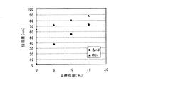
例えば、図1に示す前記延伸倍率と前記Rthおよび前記Δndとの関係に基づいて、前記条件(I)に制御することができる。図1は、前記塗工膜の延伸倍率と、位相差(Rth、Δnd)との関係を示すグラフである。具体的には、前記構造式(2)で表される繰り返し単位からなるポリイミド(重量平均分子量125,000)の溶液を、TAC基材上へ塗工して、厚み7.0μmのポリイミド塗工膜を形成させ、この塗工膜とともに前記基材を0〜15%の延伸倍率で延伸して光学補償フィルムを作製した場合における、それぞれの光学補償フィルムの位相差(Rth、Δnd)を測定した結果を示すグラフである。図1に示すとおり、延伸倍率と厚み方向位相差値Rth、延伸倍率と面内方向位相差値Δndは、それぞれ線形の関係にある。したがって、このグラフに基づき延伸倍率を調整すれば、前記(nx-nz)/(nx-ny)が制御できる。 For example, the condition (I) can be controlled based on the relationship between the draw ratio, Rth, and Δnd shown in FIG. FIG. 1 is a graph showing the relationship between the draw ratio of the coating film and the phase difference (Rth, Δnd). Specifically, a polyimide coating film having a thickness of 7.0 μm is applied by applying a polyimide (weight average molecular weight 125,000) solution consisting of repeating units represented by the structural formula (2) onto a TAC substrate. As a result of measuring the retardation (Rth, Δnd) of each optical compensation film in the case where an optical compensation film was produced by stretching the substrate together with this coating film at a stretching ratio of 0 to 15%. It is a graph which shows. As shown in FIG. 1, the draw ratio and the thickness direction retardation value Rth, and the draw ratio and the in-plane direction retardation value Δnd have a linear relationship. Therefore, the (nx-nz) / (nx-ny) can be controlled by adjusting the draw ratio based on this graph.
このようにして基板上に形成した本発明の光学補償フィルムは、そのまま前記基材との積層体として使用してもよいし、前記基材から剥離した単体層として使用してもよく、さらに、前記単体層の光学補償フィルムを、接着剤層または粘着剤層を介して他の基材等に積層して使用してもよい。前記接着剤または粘着剤としては、特に限定はなく、例えば、アクリル系、ビニルアルコール系、シリコーン系、ポリエステル系、ポリウレタン系、ポリエーテル系等のポリマー製感圧接着剤や、ゴム系感圧接着剤等が使用できる。また、これらの材料に、微粒子を含有させて光拡散性を示す接着剤層等としてもよい。これらの中でも、前記接着剤または粘着剤としては、例えば、吸湿性や耐熱性に優れる材料が好ましい。このような性質であれば、例えば、液晶表示装置に使用した場合に、吸湿による発泡や剥離、熱膨張差等による光学特性の低下や、液晶セルの反り等を防止でき、高品質で耐久性にも優れる表示装置となる。 Thus, the optical compensation film of the present invention formed on the substrate may be used as it is as a laminate with the base material, or may be used as a single layer peeled from the base material, The single layer optical compensation film may be used by being laminated on another substrate or the like via an adhesive layer or an adhesive layer. The adhesive or pressure-sensitive adhesive is not particularly limited. For example, an acrylic, vinyl alcohol, silicone, polyester, polyurethane, polyether, or other polymer pressure sensitive adhesive or rubber pressure sensitive adhesive is used. An agent can be used. Moreover, it is good also as an adhesive layer etc. which contain microparticles | fine-particles in these materials and show light diffusivity. Among these, as the adhesive or pressure-sensitive adhesive, for example, a material excellent in hygroscopicity and heat resistance is preferable. With such a property, for example, when used in a liquid crystal display device, it can prevent foaming and peeling due to moisture absorption, deterioration of optical characteristics due to a difference in thermal expansion, warpage of the liquid crystal cell, etc., and high quality and durability. The display device is also excellent.
また、本発明の光学補償フィルムは、さらに、少なくとも一方の表面に、前記接着剤層または粘着剤層を備えることが好ましい。これによって、本発明の光学補償フィルムと、光学層や液晶セル等の他部材との接着が容易になるとともに、本発明の光学フィルムの剥離を防止することができるからである。 The optical compensation film of the present invention preferably further comprises the adhesive layer or the pressure-sensitive adhesive layer on at least one surface. This is because adhesion between the optical compensation film of the present invention and other members such as an optical layer and a liquid crystal cell is facilitated, and peeling of the optical film of the present invention can be prevented.
本発明の光学補償層付偏光板は、光学フィルムを含む積層偏光板であって、前記光学フィルムが、本発明の光学補償フィルムであることを特徴とする。このような光学補償付偏光板の構成は、本発明の光学補償フィルムを有していれば、特に制限されない。また、本発明の光学補償フィルムに積層する偏光板は、例えば、偏光子のみでもよいし、偏光子の片面または両面にさらに透明保護層が積層されたものでもよい。 The polarizing plate with an optical compensation layer of the present invention is a laminated polarizing plate including an optical film, wherein the optical film is the optical compensation film of the present invention. The configuration of such a polarizing plate with optical compensation is not particularly limited as long as it has the optical compensation film of the present invention. Moreover, the polarizing plate laminated | stacked on the optical compensation film of this invention may be only a polarizer, for example, and what further laminated | stacked the transparent protective layer on the single side | surface or both surfaces of the polarizer may be sufficient.
本発明の光学補償層付偏光板としては、例えば、図2A〜Dの断面図に示すような形態があげられる。なお、同図は、前記光学補償層付偏光板を液晶セルに配置した状態を示しており、また、これらの図において同一部分には同一符号を付している。ただし、本発明の光学補償層付偏光板は、以下の構成に限定されるものではなく、例えば、さらに他の光学部材等を含んでいてもよい。 Examples of the polarizing plate with an optical compensation layer of the present invention include forms shown in the cross-sectional views of FIGS. This figure shows a state in which the polarizing plate with an optical compensation layer is arranged in a liquid crystal cell, and the same reference numerals are given to the same parts in these drawings. However, the polarizing plate with an optical compensation layer of the present invention is not limited to the following configuration, and may further include other optical members, for example.
図2Aに示す光学補償層付偏光板10は、本発明の光学補償フィルム1、基材2、2つの粘着剤層3、偏光子4および2つの透明保護層5を有しており、前記基材2の一方の表面に前記光学補償フィルム1が積層され、前記光学補償フィルム1の表面にさらに前記粘着剤層3が形成され、前記基材2の他方の表面には前記粘着剤層3を介して、両面に前記透明保護層5が積層された前記偏光子4が配置されている。そして、前記光学補償層付偏光板10は、その最外層に配置された前記粘着剤層3によって、液晶セル6に接着されている。なお、前記粘着剤層3は、接着剤層であっても良く、また、前記液晶セル6は、通常2枚のセル基板の間に液晶が担持された構成であるが、同図においてはその構成を省略する(以下同じ)。このような光学補償層付偏光板10において、例えば、光学補償フィルム1は、前述のように基材2上に直接形成させて、積層体として使用してもよい。
A
図2Bに示す光学補償層付偏光板20は、本発明の光学補償フィルム1、2つの粘着剤層3、偏光子4および2つの透明保護層5を有しており、前記光学補償フィルム1の両面に前記粘着剤層3が形成され、一方の前記粘着剤層3に、両面に前記透明保護層5が積層された前記偏光子4が配置されている。そして、前記光学補償層付偏光板20は、その最外層に配置された他方の前記粘着剤層3によって、液晶セル6に接着されている。このような光学補償層付偏光板20において、例えば、光学補償フィルム1は、基材から剥離したものを使用できる。
The
図2Cに示す光学補償層付偏光板30は、本発明の光学補償フィルム1、粘着剤層3、偏光子4および2つの透明保護層5を有しており、前記光学補償フィルム1の一方の表面に前記粘着剤層3が形成され、前記光学補償フィルム1の他方の表面に、両面に前記透明保護層5を積層した前記偏光子4が配置されている。そして、前記光学補償層付偏光板30は、その最外層に配置された前記粘着剤層3によって液晶セル6に接着されている。このような光学補償層付偏光板30において、例えば、光学補償フィルム1は、偏光子4上に配置した一方の透明保護層5を基材として、この基材上に直接形成させればよい。
The
図2Dに示す光学補償層付偏光板40は、本発明の光学補償フィルム1、粘着剤層3、偏光子4および透明保護層5を有しており、前記光学補償フィルム1の一方の表面に前記粘着剤層3が形成され、前記光学補償フィルム1の他方の表面に前記偏光子4が積層され、前記偏光子4の表面にさらに前記透明保護層5が積層されている。そして、前記光学補償付偏光板40は、その最外層に配置された前記粘着剤層3によって、液晶セル6に接着されている。このような光学補償層付偏光板40においては、光学補償フィルム1が、偏光子上の透明保護層の役割を兼ねるため、薄型化を図ることができる。
A
前記偏光子としては、特に制限されず、例えば、従来公知の方法により、各種フィルムに、ヨウ素や二色性染料等の二色性物質を吸着させて染色し、架橋、延伸、乾燥することによって調製したもの等が使用できる。この中でも、自然光を入射させると直線偏光を透過するフィルムが好ましく、光透過率や偏光度に優れるものが好ましい。前記二色性物質を吸着させる各種フィルムとしては、例えば、ポリビニルアルコール(PVA)系フィルム、部分ホルマール化PVA系フィルム、エチレン・酢酸ビニル共重合体系部分ケン化フィルム、セルロース系フィルム等の親水性高分子フィルム等があげられ、これらの他にも、例えば、PVAの脱水処理物やポリ塩化ビニルの脱塩酸処理物等のポリエン配向フィルム等も使用できる。これらの中でも、好ましくはPVA系フィルムである。また、前記偏光フィルムの厚みは、通常、1〜80μmの範囲であるが、これには限定されない。 The polarizer is not particularly limited, and for example, by dying dichroic substances such as iodine and dichroic dyes on various films by using a conventionally known method, dyeing, crosslinking, stretching, and drying. The prepared one can be used. Among these, a film that transmits linearly polarized light when natural light is incident is preferable, and a film that is excellent in light transmittance and degree of polarization is preferable. Examples of the various films that adsorb the dichroic substance include high hydrophilicity such as polyvinyl alcohol (PVA) film, partially formalized PVA film, ethylene / vinyl acetate copolymer partially saponified film, and cellulose film. In addition to these, for example, polyene oriented films such as PVA dehydrated products and polyvinyl chloride dehydrochlorinated products can be used. Among these, PVA film is preferable. Moreover, although the thickness of the said polarizing film is the range of 1-80 micrometers normally, it is not limited to this.
前記透明保護層としては、特に制限されず、従来公知の透明フィルムを使用できるが、例えば、透明性、機械的強度、熱安定性、水分遮断性、等方性などに優れるものが好ましい。このような透明保護層の材質の具体例としては、トリアセチルセルロール等のセルロース系樹脂や、ポリエステル系、ポリカーボネート系、ポリアミド系、ポリイミド系、ポリエーテルスルホン系、ポリスルホン系、ポリスチレン系、ポリノルボルネン系、ポリオレフィン系、アクリル系、アセテート系等の透明樹脂等があげられる。また、前記アクリル系、ウレタン系、アクリルウレタン系、エポキシ系、シリコーン系等の熱硬化型樹脂または紫外線硬化型樹脂等もあげられる。この中でも、偏光特性や耐久性の点から、表面をアルカリ等でケン化処理したTACフィルムが好ましい。 The transparent protective layer is not particularly limited, and a conventionally known transparent film can be used. For example, a layer having excellent transparency, mechanical strength, thermal stability, moisture barrier property, isotropy, and the like is preferable. Specific examples of the material for such a transparent protective layer include cellulose resins such as triacetyl cellulose, polyester, polycarbonate, polyamide, polyimide, polyethersulfone, polysulfone, polystyrene, and polynorbornene. Transparent resins such as polyethylene, polyolefin, acrylic, and acetate. Further, examples thereof include thermosetting resins such as acrylic, urethane, acrylic urethane, epoxy, and silicone, or ultraviolet curable resins. Among these, a TAC film whose surface is saponified with alkali or the like is preferable from the viewpoint of polarization characteristics and durability.
また、特開2001-343529号公報(WO01/37007)に記載のポリマーフィルムがあげられる。このポリマー材料としては、例えば、側鎖に置換または非置換のイミド基を有する熱可塑性樹脂と、側鎖に置換または非置換のフェニル基ならびにニトリル基を有す熱可塑性樹脂を含有する樹脂組成物が使用でき、例えば、イソブテンとN-メチルマレイミドからなる交互共重合体と、アクリロニトリル・スチレン共重合体とを有する樹脂組成物があげられる。なお、前記ポリマーフィルムは、例えば、前記樹脂組成物の押出成形物であってもよい。 Moreover, the polymer film as described in Unexamined-Japanese-Patent No. 2001-343529 (WO01 / 37007) is mention | raise | lifted. Examples of the polymer material include a resin composition containing a thermoplastic resin having a substituted or unsubstituted imide group in the side chain and a thermoplastic resin having a substituted or unsubstituted phenyl group and a nitrile group in the side chain. For example, a resin composition having an alternating copolymer composed of isobutene and N-methylmaleimide and an acrylonitrile / styrene copolymer can be used. The polymer film may be, for example, an extruded product of the resin composition.
また、前記透明保護層は、例えば、色付きが無いことが好ましい。具体的には、下記条件で表される前記透明フィルム厚み方向の位相差値(Rth')が、−90nm〜+75nmの範囲であることが好ましく、より好ましくは−80nm〜+60nmであり、特に好ましくは−70nm〜+45nmの範囲である。前記位相差値が−90nm〜+75nmの範囲であれば、十分に前記透明フィルムに起因する偏光板の着色(光学的な着色)を解消できる。なお、下記式において、nx,ny,nzは、前記透明保護層における複屈折率であって前述と同様であり、dは、その厚みをあらわす。 Moreover, it is preferable that the said transparent protective layer does not have coloring, for example. Specifically, the retardation value (Rth ′) in the transparent film thickness direction represented by the following conditions is preferably in the range of −90 nm to +75 nm, more preferably −80 nm to +60 nm, and particularly preferably. Is in the range of -70 nm to +45 nm. If the retardation value is in the range of −90 nm to +75 nm, the coloring (optical coloring) of the polarizing plate due to the transparent film can be sufficiently eliminated. In the following formula, nx, ny, and nz are birefringences in the transparent protective layer, which are the same as described above, and d represents the thickness thereof.
Rth'=[[(nx+ny)/2]-nz]d
また、前記透明保護層は、さらに光学補償機能を有するものでもよい。このように光学補償機能を有する透明保護層としては、例えば、液晶セルにおける位相差に基づく視認角の変化が原因である着色等の防止や、良視認の視野角の拡大等を目的とした公知のものが使用できる。具体的には、例えば、前述した透明樹脂を一軸延伸または二軸延伸した各種延伸フィルムや、液晶ポリマー等の配向フィルム、透明基材上に液晶ポリマー等の配向層を配置した積層体等があげられる。これらの中でも、良視認の広い視野角を達成できることから、前記液晶ポリマーの配向フィルムが好ましく、特に、ディスコティック系やネマチック系の液晶ポリマーの傾斜配向層から構成される光学補償層を、前述のトリアセチルセルロースフィルム等で支持した光学補償位相差板が好ましい。このような光学補償位相差板としては、例えば、富士写真フィルム株式会社製「WVフィルム」等の市販品があげられる。なお、前記光学補償位相差板は、前記位相差フィルムやトリアセチルセルロースフィルム等のフィルム支持体を2層以上積層させることによって、位相差等の光学特性を制御したもの等でもよい。
Rth ′ = [[(nx + ny) / 2] −nz] d
The transparent protective layer may further have an optical compensation function. As such a transparent protective layer having an optical compensation function, for example, known for the purpose of preventing coloring or the like caused by a change in viewing angle based on a phase difference in a liquid crystal cell, or widening a viewing angle for good viewing Can be used. Specifically, for example, various stretched films obtained by uniaxially or biaxially stretching the above-described transparent resin, alignment films such as liquid crystal polymers, and laminates in which alignment layers such as liquid crystal polymers are arranged on a transparent substrate. It is done. Among these, since it is possible to achieve a wide viewing angle with good visibility, the alignment film of the liquid crystal polymer is preferable, and in particular, the optical compensation layer composed of the inclined alignment layer of the discotic or nematic liquid crystal polymer is used as described above. An optical compensation retardation plate supported by a triacetyl cellulose film or the like is preferable. Examples of such an optical compensation retardation plate include commercially available products such as “WV film” manufactured by Fuji Photo Film Co., Ltd. The optical compensation retardation plate may be one in which optical properties such as retardation are controlled by laminating two or more film supports such as the retardation film and triacetyl cellulose film.
前記透明保護層の厚みは、特に制限されず、例えば、位相差や保護強度等に応じて適宜決定できるが、通常、500μm以下であり、好ましくは5〜300μm、より好ましくは5〜150μmの範囲である
前記透明保護層は、例えば、偏光フィルムに前記各種透明樹脂を塗布する方法、前記偏光フィルムに前記透明樹脂製フィルムや前記光学補償位相差板等を積層する方法等の従来公知の方法によって適宜形成でき、また市販品を使用することもできる。
The thickness of the transparent protective layer is not particularly limited, and can be appropriately determined according to, for example, the phase difference or the protective strength, but is usually 500 μm or less, preferably 5 to 300 μm, more preferably 5 to 150 μm. The transparent protective layer is formed by a conventionally known method such as a method of applying the various transparent resins to a polarizing film, a method of laminating the transparent resin film, the optical compensation phase difference plate, or the like on the polarizing film. It can form suitably and can also use a commercial item.
また、前記透明保護層は、さらに、例えば、ハードコート処理、反射防止処理、スティッキングの防止や拡散、アンチグレア等を目的とした処理等が施されたものでもよい。前記ハードコート処理とは、偏光板表面の傷付き防止等を目的とし、例えば、前記透明保護層の表面に、硬化型樹脂から構成される、硬度や滑り性に優れた硬化被膜を形成する処理である。前記硬化型樹脂としては、例えば、シリコーン系、ウレタン系、アクリル系、エポキシ系等の紫外線硬化型樹脂等が使用でき、前記処理は、従来公知の方法によって行うことができる。スティッキングの防止は、隣接する層との密着防止を目的とする。前記反射防止処理とは、偏光板表面での外光の反射防止を目的とし、従来公知の反射防止層等の形成により行うことができる。 The transparent protective layer may be further subjected to, for example, a hard coat treatment, an antireflection treatment, a treatment for preventing sticking or diffusion, antiglare, and the like. The hard coat treatment is for the purpose of preventing scratches on the surface of the polarizing plate, for example, a treatment for forming a cured film having excellent hardness and slipperiness composed of a curable resin on the surface of the transparent protective layer. It is. As the curable resin, for example, a silicone-based, urethane-based, acrylic-based, or epoxy-based ultraviolet curable resin can be used, and the treatment can be performed by a conventionally known method. The purpose of preventing sticking is to prevent adhesion between adjacent layers. The antireflection treatment is intended to prevent reflection of external light on the surface of the polarizing plate, and can be performed by forming a conventionally known antireflection layer or the like.
前記アンチグレア処理は、偏光板表面において外光が反射することによる、偏光板透過光の視認妨害を防止すること等を目的とし、例えば、従来公知の方法によって、前記透明保護層の表面に、微細な凹凸構造を形成することによって行うことができる。このような凹凸構造の形成方法としては、例えば、サンドブラスト法やエンボス加工等による粗面化方式や、前述のような透明樹脂に透明微粒子を配合して前記透明保護層を形成する方式等があげられる。 The anti-glare treatment is intended to prevent visual interference of the light transmitted through the polarizing plate due to reflection of external light on the surface of the polarizing plate. For example, the anti-glare treatment is finely applied to the surface of the transparent protective layer by a conventionally known method. This can be done by forming an uneven structure. Examples of a method for forming such a concavo-convex structure include a roughening method by sandblasting or embossing, a method of forming the transparent protective layer by blending transparent fine particles in the transparent resin as described above, and the like. It is done.
前記透明微粒子としては、例えば、シリカ、アルミナ、チタニア、ジルコニア、酸化錫、酸化インジウム、酸化カドミウム、酸化アンチモン等があげられ、この他にも導電性を有する無機系微粒子や、架橋または未架橋のポリマー粒状物等から構成される有機系微粒子等を使用することもできる。前記透明微粒子の平均粒径は、特に制限されないが、例えば、0.5〜20μmの範囲である。また、前記透明微粒子の配合割合は、特に制限されないが、一般に、前述のような透明樹脂100重量部あたり2〜70重量部の範囲が好ましく、より好ましくは5〜50重量部の範囲である。 Examples of the transparent fine particles include silica, alumina, titania, zirconia, tin oxide, indium oxide, cadmium oxide, antimony oxide, and the like. In addition, conductive inorganic fine particles, crosslinked or uncrosslinked Organic fine particles composed of polymer particles and the like can also be used. The average particle size of the transparent fine particles is not particularly limited, but is, for example, in the range of 0.5 to 20 μm. The blending ratio of the transparent fine particles is not particularly limited, but is generally preferably in the range of 2 to 70 parts by weight, more preferably in the range of 5 to 50 parts by weight per 100 parts by weight of the transparent resin as described above.
前記透明微粒子を配合したアンチグレア層は、例えば、透明保護層そのものとして使用することもでき、また、透明保護層表面に塗工層等として形成されてもよい。さらに、前記アンチグレア層は、偏光板透過光を拡散して視角を拡大するための拡散層(視覚補償機能等)を兼ねるものであってもよい。 The antiglare layer containing the transparent fine particles can be used as, for example, the transparent protective layer itself, or may be formed as a coating layer on the surface of the transparent protective layer. Furthermore, the anti-glare layer may also serve as a diffusion layer (visual compensation function or the like) for diffusing the light transmitted through the polarizing plate to expand the viewing angle.
なお、前記反射防止層、スティッキング防止層、拡散層、アンチグレア層等は、前記透明保護層とは別個に、例えば、これらの層を設けたシート等から構成される光学層として、偏光板に積層してもよい。 The antireflection layer, anti-sticking layer, diffusion layer, anti-glare layer, etc. are laminated on the polarizing plate as an optical layer composed of, for example, a sheet provided with these layers, separately from the transparent protective layer. May be.
各構成物同士(光学補償フィルム、偏光子、透明保護層等)の積層方法は、特に制限されず、従来公知の方法によって行うことができる。一般には、前述と同様の粘着剤や接着剤等が使用でき、その種類は、前記各構成物の材質等によって適宜決定できる。前記接着剤としては、例えば、アクリル系、ビニルアルコール系、シリコーン系、ポリエステル系、ポリウレタン系、ポリエーテル系等のポリマー製接着剤や、ゴム系接着剤等があげられる。また、グルタルアルデヒド、メラミン、シュウ酸等のビニルアルコール系ポリマーの水溶性架橋剤等から構成される接着剤等も使用できる。これらの接着剤や粘着剤としては、例えば、湿度や熱の影響によっても剥がれ難く、光透過率や偏光度にも優れるものが好ましい。具体的には、前記偏光子がPVA系フィルムの場合、例えば、接着処理の安定性等の点から、PVA系接着剤が好ましい。これらの接着剤や粘着剤は、例えば、そのまま偏光子や透明保護層の表面に塗布してもよいし、前記接着剤や粘着剤から構成されたテープやシートのような層を前記表面に配置してもよい。また、例えば、水溶液として調製した場合、必要に応じて、他の添加剤や、酸等の触媒を配合してもよい。なお、前記接着剤を塗布する場合は、例えば、前記接着剤水溶液に、さらに、他の添加剤や、酸等の触媒を配合してもよい。このような接着層の厚みは、特に制限されないが、例えば、1nm〜500nmであり、好ましくは10nm〜300nmであり、より好ましくは20nm〜100nmである。特に限定されず、例えば、アクリル系ポリマーやビニルアルコール系ポリマー等の接着剤等を使用した従来公知の方法が採用できる。また、湿度や熱等によっても剥がれにくく、光透過率や偏光度に優れる偏光板を形成できることから、さらに、グルタルアルデヒド、メラミン、シュウ酸等のPVA系ポリマーの水溶性架橋剤を含む接着剤が好ましい。これらの接着剤は、例えば、その水溶液を前記各構成物表面に塗工し、乾燥すること等によって使用できる。前記水溶液には、例えば、必要に応じて、他の添加剤や、酸等の触媒も配合できる。これらの中でも、前記接着剤としては、PVAフィルムとの接着性に優れる点から、PVA系接着剤が好ましい。 The method for laminating the components (optical compensation film, polarizer, transparent protective layer, etc.) is not particularly limited, and can be performed by a conventionally known method. In general, the same pressure-sensitive adhesives and adhesives as described above can be used, and the type thereof can be appropriately determined depending on the material of each component. Examples of the adhesive include polymer adhesives such as acrylic, vinyl alcohol, silicone, polyester, polyurethane, and polyether, and rubber adhesives. Further, an adhesive composed of a water-soluble crosslinking agent of vinyl alcohol polymers such as glutaraldehyde, melamine and oxalic acid can be used. As these adhesives and pressure-sensitive adhesives, for example, those that do not easily peel off due to the influence of humidity and heat and that are excellent in light transmittance and polarization degree are preferable. Specifically, when the polarizer is a PVA-based film, for example, a PVA-based adhesive is preferable from the viewpoint of the stability of the adhesion treatment. These adhesives and pressure-sensitive adhesives may be applied to the surface of the polarizer or the transparent protective layer as they are, for example, or a layer such as a tape or sheet composed of the adhesive or pressure-sensitive adhesive is disposed on the surface. May be. For example, when prepared as an aqueous solution, other additives and catalysts such as acids may be blended as necessary. In addition, when apply | coating the said adhesive agent, you may mix | blend another additive and catalysts, such as an acid, with the said adhesive agent aqueous solution, for example. The thickness of such an adhesive layer is not particularly limited, but is, for example, 1 nm to 500 nm, preferably 10 nm to 300 nm, and more preferably 20 nm to 100 nm. The method is not particularly limited, and for example, a conventionally known method using an adhesive such as an acrylic polymer or a vinyl alcohol polymer can be employed. In addition, an adhesive containing a water-soluble cross-linking agent of PVA polymer such as glutaraldehyde, melamine, oxalic acid and the like can be obtained because it can form a polarizing plate that is hardly peeled off by humidity, heat, etc. and has excellent light transmittance and polarization degree. preferable. These adhesives can be used by, for example, applying the aqueous solution to the surface of each component and drying. In the aqueous solution, for example, other additives and a catalyst such as an acid can be blended as necessary. Among these, as the adhesive, a PVA adhesive is preferable from the viewpoint of excellent adhesiveness with a PVA film.
また、本発明の光学補償フィルムは、前述のような偏光子の他にも、例えば、各種位相差板、拡散制御フィルム、輝度向上フィルム等、従来公知の光学部材と組合せて使用することもできる。前記位相差板としては、例えば、ポリマーフィルムを一軸延伸または二軸延伸したもの、Z軸配向処理したもの、液晶性高分子の塗工膜等があげられる。前記拡散制御フィルムとしては、例えば、拡散、散乱、屈折を利用したフィルムがあげられ、これらは、例えば、視野角の制御や、解像度に関わるギラツキや散乱光の制御等に使用することができる。前記輝度向上フィルムとしては、例えば、コレステリック液晶の選択反射と1/4波長板(λ/4板)とを用いた輝度向上フィルムや、偏光方向による異方性散乱を利用した散乱フィルム等が使用できる。また、前記光学フィルムは、例えば、ワイヤーグリッド型偏光子と組合せることもできる。 In addition to the polarizer as described above, the optical compensation film of the present invention can be used in combination with conventionally known optical members such as various retardation plates, diffusion control films, brightness enhancement films, and the like. . Examples of the retardation plate include a uniaxially or biaxially stretched polymer film, a Z-axis aligned treatment, a liquid crystalline polymer coating film, and the like. Examples of the diffusion control film include films utilizing diffusion, scattering, and refraction, and these can be used for, for example, control of viewing angle, glare related to resolution, and control of scattered light. As the brightness enhancement film, for example, a brightness enhancement film using selective reflection of a cholesteric liquid crystal and a quarter wavelength plate (λ / 4 plate), a scattering film using anisotropic scattering by the polarization direction, or the like is used. it can. Moreover, the said optical film can also be combined with a wire grid type polarizer, for example.
本発明の光学補償層付偏光板は、実用に際して、前記本発明の光学補償フィルムの他に、さらに他の光学層を含んでもよい。前記光学層としては、例えば、以下に示すような偏光板、反射板、半透過反射板、輝度向上フィルム等、液晶表示装置等の形成に使用される、従来公知の各種光学層があげられる。これらの光学層は、一種類でもよいし、二種類以上を併用してもよく、また、一層でもよいし、二層以上を積層してもよい。このような光学層をさらに含む積層偏光板は、例えば、光学補償機能を有する一体型偏光板として使用することが好ましく、例えば、液晶セル表面に配置する等、各種画像表示装置への使用に適している。 In practical use, the polarizing plate with an optical compensation layer of the present invention may further contain other optical layers in addition to the optical compensation film of the present invention. Examples of the optical layer include conventionally known various optical layers used for forming a liquid crystal display device and the like such as a polarizing plate, a reflecting plate, a transflective plate, and a brightness enhancement film as shown below. One kind of these optical layers may be used, two or more kinds may be used in combination, one layer may be used, or two or more layers may be laminated. The laminated polarizing plate further including such an optical layer is preferably used as an integrated polarizing plate having an optical compensation function, for example, and is suitable for use in various image display devices such as being disposed on the surface of a liquid crystal cell. ing.
以下に、このような一体型偏光板について説明する。 Hereinafter, such an integrated polarizing plate will be described.
まず、反射型偏光板または半透過反射型偏光板の一例について説明する。前記反射型偏光板は、本発明の光学補償層付偏光板にさらに反射板が、前記半透過反射型偏光板は、本発明の光学補償層付偏光板にさらに半透過反射板が、それぞれ積層されている。 First, an example of a reflective polarizing plate or a transflective polarizing plate will be described. The reflective polarizing plate is further laminated with a polarizing plate with an optical compensation layer of the present invention, and the transflective polarizing plate is further laminated with a semi-transmissive reflective plate with a polarizing plate with an optical compensation layer of the present invention. Has been.
前記反射型偏光板は、通常、液晶セルの裏側に配置され、視認側(表示側)からの入射光を反射させて表示するタイプの液晶表示装置(反射型液晶表示装置)等に使用できる。このような反射型偏光板は、例えば、バックライト等の光源の内蔵を省略できるため、液晶表示装置の薄型化を可能にする等の利点を有する。 The reflective polarizing plate is usually disposed on the back side of a liquid crystal cell, and can be used for a liquid crystal display device (reflective liquid crystal display device) of a type that reflects incident light from the viewing side (display side). Such a reflective polarizing plate, for example, has an advantage that the liquid crystal display device can be thinned because the built-in light source such as a backlight can be omitted.
前記反射型偏光板は、例えば、前記弾性率を示す偏光板の片面に、金属等から構成される反射板を形成する方法等、従来公知の方法によって作製できる。具体的には、例えば、前記偏光板における透明保護層の片面(露出面)を、必要に応じてマット処理し、前記面に、アルミニウム等の反射性金属からなる金属箔や蒸着膜を反射板として形成した反射型偏光板等があげられる。 The reflective polarizing plate can be produced by a conventionally known method such as a method of forming a reflective plate made of metal or the like on one surface of a polarizing plate exhibiting the elastic modulus. Specifically, for example, one surface (exposed surface) of the transparent protective layer in the polarizing plate is mat-treated as necessary, and a metal foil or a vapor deposition film made of a reflective metal such as aluminum is formed on the surface as a reflection plate. The reflective polarizing plate formed as follows.
また、前述のように各種透明樹脂に微粒子を含有させて表面を微細凹凸構造とした透明保護層の上に、その微細凹凸構造を反映させた反射板を形成した、反射型偏光板等もあげられる。その表面が微細凹凸構造である反射板は、例えば、入射光を乱反射により拡散させ、指向性やギラギラした見栄えを防止し、明暗のムラを抑制できるという利点を有する。このような反射板は、例えば、前記透明保護層の凹凸表面に、真空蒸着方式、イオンプレーティング方式、スパッタリング方式等の蒸着方式やメッキ方式等、従来公知の方法により、直接、前記金属箔や金属蒸着膜として形成することができる。 In addition, as described above, a reflective polarizing plate or the like in which a reflecting plate reflecting the fine uneven structure is formed on a transparent protective layer containing fine particles in various transparent resins and having a fine uneven structure on the surface. It is done. A reflector having a fine concavo-convex structure on its surface has an advantage that, for example, incident light can be diffused by irregular reflection to prevent directivity and glaring appearance and to suppress uneven brightness. Such a reflector is, for example, directly on the uneven surface of the transparent protective layer by a conventionally known method such as a vacuum deposition method, an ion plating method, a sputtering method, or a plating method. It can form as a metal vapor deposition film.
また、前述のように偏光板の透明保護層に前記反射板を直接形成する方式に代えて、反射板として、前記透明保護フィルムのような適当なフィルムに反射層を設けた反射シート等を使用してもよい。前記反射板における前記反射層は、通常、金属から構成されるため、例えば、酸化による反射率の低下防止、ひいては初期反射率の長期持続や、透明保護層の別途形成を回避する点等から、その使用形態は、前記反射層の反射面が前記フィルムや偏光板等で被覆された状態であることが好ましい。 In addition, instead of the method of directly forming the reflective plate on the transparent protective layer of the polarizing plate as described above, a reflective sheet having a reflective layer provided on a suitable film such as the transparent protective film is used as the reflective plate. May be. Since the reflective layer in the reflective plate is usually composed of metal, for example, from the viewpoint of preventing the decrease in reflectance due to oxidation, and thus the long-term persistence of the initial reflectance, and the separate formation of a transparent protective layer, etc. The usage form is preferably a state in which the reflective surface of the reflective layer is covered with the film, a polarizing plate or the like.
一方、前記半透過型偏光板は、前記反射型偏光板において、反射板に代えて、半透過型の反射板を有するものである。前記半透過型反射板としては、例えば、反射層で光を反射し、かつ、光を透過するハーフミラー等があげられる。 On the other hand, the transflective polarizing plate has a transflective reflective plate instead of the reflective plate in the reflective polarizing plate. Examples of the transflective reflector include a half mirror that reflects light through a reflective layer and transmits light.
前記半透過型偏光板は、通常、液晶セルの裏側に設けられ、液晶表示装置等を比較的明るい雰囲気で使用する場合には、視認側(表示側)からの入射光を反射して画像を表示し、比較的暗い雰囲気においては、半透過型偏光板のバックサイドに内蔵されているバックライト等の内蔵光源を使用して画像を表示するタイプの液晶表示装置等に使用できる。すなわち、前記半透過型偏光板は、明るい雰囲気下では、バックライト等の光源使用のエネルギーを節約でき、一方、比較的暗い雰囲気下においても、前記内蔵光源を用いて使用できるタイプの液晶表示装置等の形成に有用である。 The transflective polarizing plate is usually provided on the back side of a liquid crystal cell. When a liquid crystal display device or the like is used in a relatively bright atmosphere, the incident light from the viewing side (display side) is reflected to display an image. In a relatively dark atmosphere, it can be used for a liquid crystal display device of a type that displays an image using a built-in light source such as a backlight built in the back side of the transflective polarizing plate. That is, the transflective polarizing plate can save the energy of using a light source such as a backlight in a bright atmosphere, and can be used with the built-in light source in a relatively dark atmosphere. It is useful for the formation of etc.
つぎに、本発明の光学補償層付偏光板に、さらに輝度向上フィルムが積層された偏光板の一例を説明する。 Next, an example of a polarizing plate in which a brightness enhancement film is further laminated on the polarizing plate with an optical compensation layer of the present invention will be described.
前記輝度向上フィルムとしては、特に限定されず、例えば、誘電体の多層薄膜や、屈折率異方性が相違する薄膜フィルムの多層積層体のような、所定偏光軸の直線偏光を透過して、他の光は反射する特性を示すもの等が使用できる。このような輝度向上フィルムとしては、例えば、3M社製の商品名「D-BEF」等があげられる。また、コレステリック液晶層、特にコレステリック液晶ポリマーの配向フィルムや、その配向液晶層をフィルム基材上に支持したもの等が使用できる。これらは、左右一方の円偏光を反射して、他の光は透過する特性を示すものであり、例えば、日東電工社製の商品名「PCF350」、Merck社製の商品名「Transmax」等があげられる。 The brightness enhancement film is not particularly limited, and for example, a linear multi-layer thin film of dielectric material or a multi-layer laminate of thin film films having different refractive index anisotropy transmits linearly polarized light having a predetermined polarization axis, Other light can be used that reflects light. As such a brightness enhancement film, for example, trade name “D-BEF” manufactured by 3M Co., Ltd. may be mentioned. Also, a cholesteric liquid crystal layer, in particular an oriented film of a cholesteric liquid crystal polymer, or a film in which the oriented liquid crystal layer is supported on a film substrate can be used. These reflect the right and left circularly polarized light and transmit the other light. For example, the product name “PCF350” manufactured by Nitto Denko Corporation, the product name “Transmax” manufactured by Merck, etc. can give.
以上のような本発明の各種偏光板は、例えば、本発明の光学補償層付偏光板と、さらに2層以上の光学層とを積層した光学部材であってもよい。 The various polarizing plates of the present invention as described above may be, for example, optical members obtained by laminating the polarizing plate with an optical compensation layer of the present invention and two or more optical layers.
このように2層以上の光学層を積層した光学部材は、例えば、液晶表示装置等の製造過程において、順次別個に積層する方式によっても形成できるが、予め積層した光学部材として使用すれば、例えば、品質の安定性や組立作業性等に優れ、液晶表示装置等の製造効率を向上できるという利点がある。なお、積層には、前述と同様に、粘着層等の各種接着手段を用いることができる。 An optical member in which two or more optical layers are laminated in this manner can be formed by a method of sequentially laminating separately, for example, in the manufacturing process of a liquid crystal display device or the like. There are advantages such as excellent quality stability and assembly workability, and improvement in manufacturing efficiency of liquid crystal display devices and the like. For the lamination, various adhesive means such as an adhesive layer can be used as described above.
前述のような各種偏光板は、例えば、液晶セル等の他の部材への積層が容易になることから、さらに粘着剤層や接着剤層を有していることが好ましく、これらは、前記偏光板の片面または両面に配置することができる。前記粘着層の材料としては、特に制限されず、アクリル系ポリマー等の従来公知の材料が使用でき、特に、吸湿による発泡や剥離の防止、熱膨張差等による光学特性の低下や液晶セルの反り防止、ひいては高品質で耐久性に優れる液晶表示装置の形成性等の点より、例えば、吸湿率が低くて耐熱性に優れる粘着層となることが好ましい。また、微粒子を含有して光拡散性を示す粘着層等でもよい。前記偏光板表面への前記粘着剤層の形成は、例えば、各種粘着材料の溶液または溶融液を、流延や塗工等の展開方式により、前記偏光板の所定の面に直接添加して層を形成する方式や、同様にして後述するセパレータ上に粘着剤層を形成させて、それを前記偏光板の所定面に移着する方式等によって行うことができる。なお、このような層は、偏光板のいずれの表面に形成してもよく、例えば、偏光板における前記位相差板の露出面に形成してもよい。 The various polarizing plates as described above preferably have a pressure-sensitive adhesive layer or an adhesive layer because they can be easily laminated on other members such as a liquid crystal cell. It can be placed on one or both sides of the plate. The material of the adhesive layer is not particularly limited, and a conventionally known material such as an acrylic polymer can be used. In particular, foaming and peeling due to moisture absorption are prevented, optical characteristics are deteriorated due to a difference in thermal expansion, and a liquid crystal cell is warped. For example, it is preferable to form a pressure-sensitive adhesive layer having a low moisture absorption rate and excellent heat resistance, for example, from the viewpoints of prevention, and hence formability of a liquid crystal display device having high quality and excellent durability. Moreover, the adhesion layer etc. which contain microparticles | fine-particles and show light diffusibility may be sufficient. The pressure-sensitive adhesive layer is formed on the surface of the polarizing plate by, for example, adding a solution or a melt of various pressure-sensitive adhesive materials directly to a predetermined surface of the polarizing plate by a developing method such as casting or coating. In the same manner, a pressure-sensitive adhesive layer is formed on a separator, which will be described later, and transferred to a predetermined surface of the polarizing plate. Such a layer may be formed on any surface of the polarizing plate, for example, on the exposed surface of the retardation plate in the polarizing plate.
このように偏光板に設けた粘着剤層等の表面が露出する場合は、前記粘着層を実用に供するまでの間、汚染防止等を目的として、セパレータによって前記表面をカバーすることが好ましい。このセパレータは、前記透明保護フィルム等のような適当なフィルムに、必要に応じて、シリコーン系、長鎖アルキル系、フッ素系、硫化モリブデン等の剥離剤による剥離コートを一層以上設ける方法等によって形成できる。 Thus, when the surface of the pressure-sensitive adhesive layer or the like provided on the polarizing plate is exposed, it is preferable to cover the surface with a separator for the purpose of preventing contamination until the pressure-sensitive adhesive layer is put to practical use. This separator is formed on a suitable film such as the above-mentioned transparent protective film by a method of providing one or more release coats with a release agent such as silicone, long chain alkyl, fluorine, molybdenum sulfide, etc., if necessary. it can.
前記粘着剤層等は、例えば、単層体でもよいし、積層体でもよい。前記積層体としては、例えば、異なる組成や異なる種類の単層を組合せた積層体を使用することもできる。また、前記偏光板の両面に配置する場合は、例えば、それぞれ同じ粘着剤層でもよいし、異なる組成や異なる種類の粘着剤層であってもよい。 For example, the pressure-sensitive adhesive layer may be a single layer or a laminate. As the laminate, for example, a laminate in which different compositions and different types of single layers are combined can be used. Moreover, when arrange | positioning on the both surfaces of the said polarizing plate, the same adhesive layer may respectively be sufficient, for example, a different composition and a different kind of adhesive layer may be sufficient.
前記粘着剤層の厚みは、例えば、偏光板の構成等に応じて適宜に決定でき、一般には、1〜500μmである。 The thickness of the pressure-sensitive adhesive layer can be appropriately determined according to, for example, the configuration of the polarizing plate, and is generally 1 to 500 μm.
前記粘着剤層を形成する粘着剤としては、例えば、光学的透明性に優れ、適度な濡れ性、凝集性や接着性の粘着特性を示すものが好ましい。具体的な例としては、アクリル系ポリマーやシリコーン系ポリマー、ポリエステル、ポリウレタン、ポリエーテル、合成ゴム等のポリマーを適宜ベースポリマーとして調製された粘着剤等があげられる。 As the pressure-sensitive adhesive that forms the pressure-sensitive adhesive layer, for example, one that is excellent in optical transparency and exhibits appropriate wettability, cohesiveness, and adhesive pressure-sensitive adhesive properties is preferable. Specific examples include pressure-sensitive adhesives prepared by appropriately using polymers such as acrylic polymers, silicone polymers, polyesters, polyurethanes, polyethers, and synthetic rubbers as base polymers.
前記粘着剤層の粘着特性の制御は、例えば、前記粘着剤層を形成するベースポリマーの組成や分子量、架橋方式、架橋性官能基の含有割合、架橋剤の配合割合等によって、その架橋度や分子量を調節するというような、従来公知の方法によって適宜行うことができる。 Control of the adhesive property of the pressure-sensitive adhesive layer is, for example, the degree of cross-linking depending on the composition and molecular weight of the base polymer forming the pressure-sensitive adhesive layer, the crosslinking method, the content ratio of the crosslinkable functional group, the blending ratio of the crosslinking agent, and the like. It can be suitably carried out by a conventionally known method such as adjusting the molecular weight.
また、本発明の光学補償フィルムは、そのフィルム上に液晶材料を塗布して、ポリイミド層と液晶層とからなる複合位相差板として機能させれば、液晶配向膜を兼ねたものとして使用できる。前記複合位相差板とする際に、前記光学補償フィルムに、新たに配向処理を追加して行ってもよい。前記配向処理としては、例えば、ラビング処理や、偏光紫外光照射等を用いることができる。 The optical compensation film of the present invention can also be used as a liquid crystal alignment film by applying a liquid crystal material on the film and functioning as a composite retardation plate composed of a polyimide layer and a liquid crystal layer. When the composite retardation plate is used, an alignment treatment may be newly added to the optical compensation film. As the alignment treatment, for example, rubbing treatment, polarized ultraviolet light irradiation, or the like can be used.
以上のような本発明の光学補償フィルムや光学補償層付偏光板、各種光学部材(光学層を積層した各種偏光板)を形成する偏光フィルム、透明保護層、光学層、粘着剤層等の各層は、例えば、サリチル酸エステル系化合物、ベンゾフェノン系化合物、ベンゾトリアゾール系化合物、シアノアクリレート系化合物、ニッケル錯塩系化合物等の紫外線吸収剤で適宜処理することによって、紫外線吸収能を持たせたものであってもよい。 Each layer such as the optical compensation film of the present invention, a polarizing plate with an optical compensation layer, a polarizing film forming various optical members (various polarizing plates laminated with optical layers), a transparent protective layer, an optical layer, an adhesive layer and the like. Is, for example, given UV absorption ability by appropriately treating with UV absorbers such as salicylic acid ester compounds, benzophenone compounds, benzotriazole compounds, cyanoacrylate compounds, nickel complex compounds, etc. Also good.
本発明の光学補償フィルムや光学補償層付偏光板は、前述のように、液晶表示装置等の各種装置の形成に使用することが好ましく、例えば、本発明の光学フィルムや偏光板を液晶セルの片側または両側に配置して液晶パネルとし、反射型や半透過型、あるいは透過・反射両用型等の液晶表示装置に用いることができる。 As described above, the optical compensation film or polarizing plate with an optical compensation layer of the present invention is preferably used for forming various devices such as a liquid crystal display device. For example, the optical film or polarizing plate of the present invention is used in a liquid crystal cell. A liquid crystal panel is provided by being arranged on one side or both sides, and can be used for a liquid crystal display device such as a reflection type, a transflective type, or a transmission / reflection type.
液晶表示装置を形成する前記液晶セルの種類は、任意で選択でき、例えば、薄膜トランジスタ型に代表されるアクティブマトリクス駆動型のもの、ツイストネマチック型やスーパーツイストネマチック型に代表される単純マトリクス駆動型のもの等、種々のタイプの液晶セルが使用できる。これらの中でも、本発明の光学補償フィルムや光学補償層付偏光板は、特にVA(垂直配向;Vertical Alighned)セルの光学補償に非常に優れているので、VAモードの液晶表示装置用の視角補償フィルムとして非常に有用である。 The type of the liquid crystal cell forming the liquid crystal display device can be arbitrarily selected. For example, an active matrix driving type represented by a thin film transistor type, a simple matrix driving type represented by a twist nematic type or a super twist nematic type, and the like. Various types of liquid crystal cells can be used. Among these, the optical compensation film and the polarizing plate with an optical compensation layer of the present invention are particularly excellent in optical compensation of a VA (Vertical Aligned) cell, so that viewing angle compensation for a VA mode liquid crystal display device is achieved. It is very useful as a film.
また、前記液晶セルは、通常、対向する液晶セル基板の間隙に液晶が注入された構造であって、前記液晶セル基板としては、特に制限されず、例えば、ガラス基板やプラスチック基板が使用できる。なお、前記プラスチック基板の材質としては、特に制限されず、従来公知の材料があげられる。 In addition, the liquid crystal cell has a structure in which liquid crystal is usually injected into a gap between opposing liquid crystal cell substrates, and the liquid crystal cell substrate is not particularly limited, and for example, a glass substrate or a plastic substrate can be used. The material for the plastic substrate is not particularly limited, and conventionally known materials can be used.
また、液晶セルの両面に偏光板や光学部材を設ける場合、それらは同じ種類のものでもよいし、異なっていてもよい。さらに、液晶表示装置の形成に際しては、例えば、プリズムアレイシートやレンズアレイシート、光拡散板やバックライト等の適当な部品を、適当な位置に1層または2層以上配置することができる。 Moreover, when providing a polarizing plate and an optical member on both surfaces of a liquid crystal cell, they may be the same kind and may differ. Furthermore, when forming the liquid crystal display device, for example, appropriate components such as a prism array sheet, a lens array sheet, a light diffusing plate, and a backlight can be arranged in one or more layers at appropriate positions.
さらに、本発明の液晶表示装置は、液晶パネルを含み、前記液晶パネルとして、本発明の液晶パネルを使用する以外は、特に制限されない。光源を含む場合、特に制限されないが、例えば、光のエネルギーが有効に使用できることから、例えば、偏光を出射する平面光源であることが好ましい。 Furthermore, the liquid crystal display device of the present invention includes a liquid crystal panel, and is not particularly limited except that the liquid crystal panel of the present invention is used as the liquid crystal panel. In the case of including a light source, the light source is not particularly limited. However, for example, a planar light source that emits polarized light is preferable because light energy can be used effectively.
本発明の液晶表示装置は、視認側の光学フィルム(偏光板)の上に、例えば、さらに拡散板、アンチグレア層、反射防止膜、保護層や保護板を配置したり、または液晶パネルにおける液晶セルと偏光板との間に補償用位相差板等を適宜配置することもできる。 In the liquid crystal display device of the present invention, for example, a diffusion plate, an antiglare layer, an antireflection film, a protective layer and a protective plate are further arranged on the viewing-side optical film (polarizing plate), or a liquid crystal cell in a liquid crystal panel. A compensation retardation plate or the like may be appropriately disposed between the polarizing plate and the polarizing plate.
なお、本発明の光学補償フィルムや光学補償層付偏光板は、前述のような液晶表示装置には限定されず、例えば、有機エレクトロルミネッセンス(EL)ディスプレイ、PDP、FED等の自発光型表示装置にも使用できる。なお、これらの装置の構成は、従来光学補償フィルムや光学補償層付偏光板にかえて本発明の光学補償フィルム等を使用する以外は、何ら制限されない。また、自発光型フラットディスプレイに使用する場合は、例えば、本発明の複屈折性光学フィルムの面内位相差値Δndをλ/4にすることで、円偏光を得ることができるため、反射防止フィルターとして利用できる。 The optical compensation film and the polarizing plate with an optical compensation layer of the present invention are not limited to the liquid crystal display device as described above. For example, a self-luminous display device such as an organic electroluminescence (EL) display, PDP, or FED. Can also be used. In addition, the structure of these apparatuses is not restrict | limited at all except using the optical compensation film of this invention instead of the conventional optical compensation film and the polarizing plate with an optical compensation layer. In addition, when used in a self-luminous flat display, for example, by setting the in-plane retardation value Δnd of the birefringent optical film of the present invention to λ / 4, circularly polarized light can be obtained. Can be used as a filter.
次に、本発明を実施例および比較例により更に詳しく説明するが、本発明は、以下の実施例に限定されるものではない。なお、位相差値は、以下のように測定した。
(光学特性測定方法)
フィルム面内の位相差Δndおよび厚み方向の位相差Rthの値は、各実施例、比較例、参考例で得られた基材上のフィルムを、アクリル系粘着剤を介して、前記基材からガラス板に転写し、ガラス板と前記フィルムとの積層体として測定した。この測定には、王子計測機器社製商品名KOBRA−21ADHを用いて、測定波長λ=590で行った。なお、前記測定に用いたアクリル系粘着剤付ガラス板は、予めその光学特性を測定したところ、面内および厚み方向においてほぼ等方的であった。
EXAMPLES Next, although an Example and a comparative example demonstrate this invention further in detail, this invention is not limited to a following example. The phase difference value was measured as follows.
(Optical characteristics measurement method)
The values of retardation Δnd in the film plane and retardation Rth in the thickness direction are determined from the above-mentioned base material through the acrylic adhesive, and the film on the base material obtained in each example, comparative example, and reference example. It transferred to the glass plate and measured as a laminated body of a glass plate and the said film. This measurement was performed at a measurement wavelength λ = 590 using a trade name KOBRA-21ADH manufactured by Oji Scientific Instruments. In addition, when the optical characteristic was previously measured for the glass plate with an acrylic adhesive used for the said measurement, it was substantially isotropic in the surface and thickness direction.
2,2-ビス(3,4-ジカルボキシフェニル)ヘキサフルオロプロパン二無水物(6FDA)および2,2'-ビス(トリフルオロメチル)-4,4'-ジアミノビフェニル(PFMBまたはTFMB)から合成された下記一般式(8)で表されるポリイミド(重量平均分子量Mw=177,000)を、メチルイソブチルケトン(MIBK)溶媒に溶解し、14質量%溶液を調製した。このポリイミド溶液を、厚み約80μmのTAC基材(商品名フジダック、富士写真フィルム(株)社製)に塗布厚み47μmで直接塗布し、100℃で5分間加熱乾燥して前記基材上にポリイミドフィルムを得た。次に、このポリイミドフィルムを前記基材とともに150℃に加熱し、4%の自由端一軸延伸をおこない、延伸された基材上に厚み6.6μmの光学補償フィルムを得た。この光学補償フィルムの光学特性は、Δnd=50.0nm、Rth=300.0、(nx-nz)/(nx-ny)=6.0であった。 Synthesis from 2,2-bis (3,4-dicarboxyphenyl) hexafluoropropane dianhydride (6FDA) and 2,2'-bis (trifluoromethyl) -4,4'-diaminobiphenyl (PFMB or TFMB) The polyimide represented by the following general formula (8) (weight average molecular weight Mw = 177,000) was dissolved in a methyl isobutyl ketone (MIBK) solvent to prepare a 14 mass% solution. This polyimide solution was directly applied to a TAC substrate having a thickness of about 80 μm (trade name: Fuji Duck, manufactured by Fuji Photo Film Co., Ltd.) with a coating thickness of 47 μm, and heated and dried at 100 ° C. for 5 minutes to form a polyimide on the substrate. A film was obtained. Next, this polyimide film was heated to 150 ° C. together with the base material and subjected to 4% free end uniaxial stretching to obtain an optical compensation film having a thickness of 6.6 μm on the stretched base material. The optical properties of this optical compensation film were Δnd = 50.0 nm, Rth = 300.0, (nx-nz) / (nx-ny) = 6.0.
自由端一軸延伸の延伸倍率を6%とした以外は、実施例1と同様にして実施し、延伸された基材上に厚み5.6μmの光学補償フィルムを得た。この光学補償フィルムの光学特性は、Δnd=60.3nm、Rth=250.2nm、(nx-nz)/(nx-ny)=4.1であった。 An optical compensation film having a thickness of 5.6 μm was obtained on the stretched substrate, except that the stretch ratio of free end uniaxial stretching was changed to 6%. The optical properties of this optical compensation film were Δnd = 60.3 nm, Rth = 250.2 nm, (nx-nz) / (nx-ny) = 4.1.
TAC基材上への塗布厚みを30μmにした以外は、実施例1と同様にして実施し、延伸された基材上に厚み4.2μmの光学補償フィルムを得た。この光学補償フィルムの光学特性は、Δnd=50.8nm、Rth=187.7nm、(nx-nz)/(nx-ny)=3.7であった。 The same procedure as in Example 1 was conducted except that the coating thickness on the TAC substrate was changed to 30 μm, and an optical compensation film having a thickness of 4.2 μm was obtained on the stretched substrate. The optical properties of this optical compensation film were Δnd = 50.8 nm, Rth = 187.7 nm, (nx-nz) / (nx-ny) = 3.7.
(比較例1)
自由端一軸延伸の延伸倍率を2%とした以外は、実施例1と同様にして実施し、延伸された基材上に厚み5.2μmの光学補償フィルムを得た。この光学補償フィルムの光学特性は、Δnd=18.1nm、Rth=176.7nm、(nx-nz)/(nx-ny)=9.8であった。
(Comparative Example 1)
An optical compensation film having a thickness of 5.2 μm was obtained on the stretched substrate, except that the stretch ratio of free end uniaxial stretching was 2%. The optical properties of this optical compensation film were Δnd = 18.1 nm, Rth = 176.7 nm, and (nx-nz) / (nx-ny) = 9.8.
(比較例2)
自由端一軸延伸の延伸倍率を10%とした以外は、実施例1と同様にして実施し、延伸された基材上に厚み4.7μmの光学補償フィルムを得た。この光学補償フィルムの光学特性は、Δnd=87.1nm、Rth=209.3nm、(nx-nz)/(nx-ny)=2.4であった。
(Comparative Example 2)
The optical compensation film having a thickness of 4.7 μm was obtained on the stretched base material except that the stretching ratio of the free end uniaxial stretching was changed to 10%. The optical properties of this optical compensation film were Δnd = 87.1 nm, Rth = 209.3 nm, and (nx-nz) / (nx-ny) = 2.4.
実施例1〜3および比較例1〜2で得られた光学補償フィルムと、偏光板(日東電工社製、商品名HEG1425DU)とを、それぞれアクリル系粘着剤を介して積層して光学補償層付偏光板を得た。そして、これらの光学補償層付偏光板を、VAモードの液晶セルに、前記偏光板が外側になるようにして接着して、液晶表示装置を作製した。得られた液晶表示装置に白画像および黒画像を表示させ、輝度計(商品名EzContrast160D、ELDI社製)により、XYZ表示系におけるY値、x値、y値を測定し、白画像におけるY値(Yw)と黒画像におけるY値(Yb)とから、コントラスト比を、Yw/Ybとして求めた。そして、表示画面の法線を基準として全方位に0〜80°の範囲で傾斜させた方向から測定したコントラスト比が10以上となる場合を○、ならない場合を×として評価した。その結果を下記表1および図3に示す。図3Aは、実施例1〜3の光学補償フィルムを用いた液晶表示装置のコントラスト比の一例を示す図であり、図3Bは、比較例1〜2の光学補償フィルムを用いた場合の一例を示す図である。下記表1および図3に示す通り、実施例1〜3の光学補償フィルムを使用した液晶表示装置では、比較例1〜2の光学補償フィルムを使用した液晶表示装置に比べ、斜視方向からのコントラストの向上が認められた。 The optical compensation film obtained in Examples 1 to 3 and Comparative Examples 1 and 2 and a polarizing plate (manufactured by Nitto Denko Corporation, trade name HEG1425DU) are laminated via an acrylic adhesive, respectively, with an optical compensation layer. A polarizing plate was obtained. Then, these polarizing plates with an optical compensation layer were bonded to a VA mode liquid crystal cell so that the polarizing plate was on the outside, and a liquid crystal display device was produced. A white image and a black image are displayed on the obtained liquid crystal display device, and the Y value, x value, and y value in the XYZ display system are measured by a luminance meter (trade name EzContrast 160D, manufactured by ELDI), and the Y value in the white image is measured. The contrast ratio was determined as Yw / Yb from (Yw) and the Y value (Yb) in the black image. Then, the case where the contrast ratio measured from the direction tilted in the range of 0 to 80 ° in all directions with respect to the normal line of the display screen was 10 or more was evaluated as ◯, and the case where it was not evaluated was evaluated as ×. The results are shown in Table 1 below and FIG. FIG. 3A is a diagram illustrating an example of a contrast ratio of a liquid crystal display device using the optical compensation films of Examples 1 to 3, and FIG. 3B is an example of the case where the optical compensation films of Comparative Examples 1 and 2 are used. FIG. As shown in the following Table 1 and FIG. 3, in the liquid crystal display devices using the optical compensation films of Examples 1 to 3, the contrast from the perspective direction is larger than the liquid crystal display devices using the optical compensation films of Comparative Examples 1 and 2. Improvement was observed.
(表1)
d(厚み) (nx-ny)・d (nx-nz)・d (nx-nz)/(nx-ny) 全方位80度
μm nm nm の視野角
実施例1 6.6 50.0 300.0 6.0 ○
実施例2 5.6 60.3 250.2 4.1 ○
実施例3 4.2 50.8 187.7 3.7 ○
比較例1 5.2 18.1 176.7 9.8 ×
比較例2 4.7 87.1 209.3 2.4 ×
(Table 1)
d (thickness) (nx-ny), d (nx-nz), d (nx-nz) / (nx-ny) 80 degrees in all directions
Viewing angle of μm nm nm
Example 1 6.6 50.0 300.0 6.0 ○
Example 2 5.6 60.3 250.2 4.1 ○
Example 3 4.2 50.8 187.7 3.7 ○
Comparative Example 1 5.2 18.1 176.7 9.8 ×
Comparative Example 2 4.7 87.1 209.3 2.4 ×
以上説明したとおり、本発明の光学補償フィルムは、他の位相差フィルムと組み合わせなくとも優れた光学特性を有する。このため、本発明の光学補償フィルムや光学補償層付偏光板を液晶表示装置に用いれば、1枚のみで液晶表示装置の斜視方向からのコントラスト低下や、斜めから見た場合の黒表示部におけるカラーシフト等を改善でき、その結果、表示品位の視野角依存性を改善できる。さらに、本発明の光学補償層は、薄型化が可能であるから、前記液晶表示装置の薄型化、低コスト化が可能となる。 As described above, the optical compensation film of the present invention has excellent optical characteristics without being combined with other retardation films. For this reason, if the optical compensation film or polarizing plate with an optical compensation layer of the present invention is used in a liquid crystal display device, the contrast of the liquid crystal display device from the perspective direction is reduced with only one sheet, or in the black display portion when viewed from an oblique direction. Color shift and the like can be improved, and as a result, the viewing angle dependency of display quality can be improved. Furthermore, since the optical compensation layer of the present invention can be thinned, the liquid crystal display device can be thinned and reduced in cost.
1 光学補償フィルム
2 基材
3 粘着剤層
4 偏光子
5 保護フィルム
6 液晶セル
DESCRIPTION OF SYMBOLS 1 Optical compensation film 2 Base material 3 Adhesive layer 4
Claims (18)
厚みが、2〜10μmの範囲であり、
ポリイミド、ポリエーテルケトン、ポリアミドイミドおよびポリエステルイミドからなる群から選択される少なくとも一種のポリマー材料を含む形成材料から形成され、
下記条件(I)から(III)の全てを満たすことを特徴とするVAモード液晶表示装置用光学補償フィルム。
3<(nx−nz)/(nx−ny)<6 (I)
100nm≦(nx−nz)d≦400nm (II)
nx>ny>nz (III)
上記条件(I)から(III)中、nx、nyおよびnzは、それぞれ、前記光学補償フィルムにおけるX軸、Y軸およびZ軸方向の屈折率を示し、前記X軸とは、前記光学補償フィルムの面内において最大の屈折率を示す軸方向であり、Y軸は、前記面内において前記X軸に対して垂直な軸方向であり、Z軸は、前記X軸およびY軸に垂直な厚み方向を示す。また、上記条件(II)中、(nx−nz)dは、厚み方向の位相差値(Rth)であって、dは、前記光学補償フィルムの厚みを示す。 An optical compensation film for a VA (vertical alignment) mode liquid crystal display device ,
The thickness is in the range of 2-10 μm;
Formed from a forming material comprising at least one polymer material selected from the group consisting of polyimide, polyetherketone, polyamideimide and polyesterimide ,
An optical compensation film for a VA mode liquid crystal display device satisfying all of the following conditions (I) to (III) .
3 <(nx-nz) / (nx-ny) < 6 (I)
100 nm ≦ (nx−nz) d ≦ 400 nm (II)
nx>ny> nz (III)
In the above conditions (I) to (III) , nx, ny, and nz respectively indicate refractive indexes in the X-axis, Y-axis, and Z-axis directions of the optical compensation film, and the X-axis is the optical compensation film In which the Y axis is an axial direction perpendicular to the X axis and the Z axis is a thickness perpendicular to the X axis and the Y axis. Indicates direction. In the above condition (II), (nx−nz) d is a retardation value (Rth) in the thickness direction, and d indicates the thickness of the optical compensation film.
3<(nx−nz)/(nx−ny)≦4.13 <(nx−nz) / (nx−ny) ≦ 4.1 (IV)(IV)
100nm≦(nx−nz)d≦300nm100 nm ≦ (nx−nz) d ≦ 300 nm (V)(V)
Priority Applications (1)
| Application Number | Priority Date | Filing Date | Title |
|---|---|---|---|
| JP2003345875A JP3746050B2 (en) | 2003-10-03 | 2003-10-03 | Optical compensation film, polarizing plate with optical compensation layer using the same, and liquid crystal display device using the same |
Applications Claiming Priority (1)
| Application Number | Priority Date | Filing Date | Title |
|---|---|---|---|
| JP2003345875A JP3746050B2 (en) | 2003-10-03 | 2003-10-03 | Optical compensation film, polarizing plate with optical compensation layer using the same, and liquid crystal display device using the same |
Publications (3)
| Publication Number | Publication Date |
|---|---|
| JP2005114836A JP2005114836A (en) | 2005-04-28 |
| JP2005114836A5 JP2005114836A5 (en) | 2005-09-22 |
| JP3746050B2 true JP3746050B2 (en) | 2006-02-15 |
Family
ID=34539012
Family Applications (1)
| Application Number | Title | Priority Date | Filing Date |
|---|---|---|---|
| JP2003345875A Expired - Fee Related JP3746050B2 (en) | 2003-10-03 | 2003-10-03 | Optical compensation film, polarizing plate with optical compensation layer using the same, and liquid crystal display device using the same |
Country Status (1)
| Country | Link |
|---|---|
| JP (1) | JP3746050B2 (en) |
Families Citing this family (7)
| Publication number | Priority date | Publication date | Assignee | Title |
|---|---|---|---|---|
| JP4859038B2 (en) * | 2005-07-19 | 2012-01-18 | 日東電工株式会社 | Polarizing plate and image display device |
| JP5025390B2 (en) * | 2006-09-06 | 2012-09-12 | 富士フイルム株式会社 | Liquid crystal display |
| JPWO2008032848A1 (en) * | 2006-09-15 | 2010-01-28 | Mgcフィルシート株式会社 | Retardation film |
| JP5644064B2 (en) * | 2009-06-09 | 2014-12-24 | 住友化学株式会社 | Liquid crystal display device and polarizing plate used therefor |
| KR101909074B1 (en) * | 2013-08-26 | 2018-10-18 | 후지필름 가부시키가이샤 | Luminance-enhancing film, optical sheet member, and liquid crystal display device |
| EP2876129B1 (en) * | 2013-11-25 | 2021-05-12 | Samsung Electronics Co., Ltd. | Composition for preparing polyimide, polyimide, and article including same |
| KR102276288B1 (en) | 2013-11-25 | 2021-07-12 | 삼성전자주식회사 | Composition of preparing polyimide, polyimide, article includong same, and display device |
Family Cites Families (13)
| Publication number | Priority date | Publication date | Assignee | Title |
|---|---|---|---|---|
| US5344916A (en) * | 1993-04-21 | 1994-09-06 | The University Of Akron | Negative birefringent polyimide films |
| JPH10268135A (en) * | 1997-03-24 | 1998-10-09 | Nitto Denko Corp | Bonded compensation polarizing plate |
| JPH10293211A (en) * | 1997-04-17 | 1998-11-04 | Nitto Denko Corp | Polarizing element, illuminator and liquid crystal display device |
| JPH10319235A (en) * | 1997-05-16 | 1998-12-04 | Nitto Denko Corp | Polarizing element, lighting device, and liquid crystal display device |
| JP3591699B2 (en) * | 1997-10-09 | 2004-11-24 | 日東電工株式会社 | Polarizing element, optical element, illumination device, and liquid crystal display device |
| JP2001272538A (en) * | 2000-03-27 | 2001-10-05 | Nitto Denko Corp | Phase difference plate, optical compensating polarizing plate and liquid crystal display device |
| JP3762751B2 (en) * | 2002-01-23 | 2006-04-05 | 日東電工株式会社 | Manufacturing method of optical film |
| JP4077244B2 (en) * | 2002-05-24 | 2008-04-16 | 日東電工株式会社 | VA mode optical film, laminated polarizing plate, and image display device using the same |
| JP3764440B2 (en) * | 2002-05-24 | 2006-04-05 | 日東電工株式会社 | Manufacturing method of optical film |
| JP4070510B2 (en) * | 2002-05-24 | 2008-04-02 | 日東電工株式会社 | Birefringent film, optical compensation layer integrated polarizing plate, image display device, and method for producing birefringent film |
| JP4233431B2 (en) * | 2003-04-01 | 2009-03-04 | 日東電工株式会社 | Optical element, polarizing element, illumination device, and liquid crystal display device |
| JP2004309800A (en) * | 2003-04-07 | 2004-11-04 | Nitto Denko Corp | Method for manufacturing optical compensation film and optical compensation film |
| JP2005070096A (en) * | 2003-08-25 | 2005-03-17 | Sumitomo Chemical Co Ltd | Retardation plate integrated polarizing plate, method for manufacturing same, and liquid crystal display device |
-
2003
- 2003-10-03 JP JP2003345875A patent/JP3746050B2/en not_active Expired - Fee Related
Also Published As
| Publication number | Publication date |
|---|---|
| JP2005114836A (en) | 2005-04-28 |
Similar Documents
| Publication | Publication Date | Title |
|---|---|---|
| JP4044485B2 (en) | Optical film, method for producing the same, and polarizing plate using the same | |
| KR100801912B1 (en) | Phase difference film and production method therefor | |
| KR100618368B1 (en) | Optical film and its manufacturing method | |
| JP4236098B2 (en) | Birefringent optical film | |
| KR100618366B1 (en) | Optical film, laminated polarizing plate, liquid crystal panel, liquid crystal display, self-light-emitting display, and manufacturing method of optical film | |
| JP3762751B2 (en) | Manufacturing method of optical film | |
| KR100720887B1 (en) | Process for producing birefringent film | |
| JP4236101B2 (en) | Manufacturing method of viewing angle compensation film for VA mode liquid crystal display device | |
| JP3701022B2 (en) | Manufacturing method of birefringent optical film, film obtained by the manufacturing method, elliptically polarizing plate using the same, and liquid crystal display device using them | |
| JP2008242463A (en) | Birefringent optical film, elliptically polarized plate using same and liquid crystal display using them | |
| JP3838508B2 (en) | Manufacturing method of laminated retardation plate | |
| JP4025699B2 (en) | Liquid crystal panel and liquid crystal display device using the same | |
| KR100755769B1 (en) | Graded optical compensation film, process for producing the same and liquid crystal display including the same | |
| JP2004046097A (en) | Laminated retardation plate, stacked polarizing plate using same, and image display device | |
| JP2003315554A (en) | Stacked polarizing plate and image display device using the same | |
| JP3897743B2 (en) | Manufacturing method of optical film | |
| JP3917089B2 (en) | Method for manufacturing tilted optical compensation film | |
| JP3929046B2 (en) | Method for producing birefringent film, birefringent film, polarizing plate with optical compensation layer using the same, liquid crystal panel for vertical alignment mode liquid crystal display device, and vertical alignment mode liquid crystal display device | |
| JP2006195478A (en) | Method of manufacturing optical film | |
| JP2005258459A (en) | Method of manufacturing optical film | |
| JP3764440B2 (en) | Manufacturing method of optical film | |
| JP3746050B2 (en) | Optical compensation film, polarizing plate with optical compensation layer using the same, and liquid crystal display device using the same | |
| JP2008171007A (en) | Method of manufacturing birefringent film | |
| JP4274842B2 (en) | Polarizing plate with optical compensation function for VA mode liquid crystal display device, and VA mode liquid crystal display device using the same | |
| JP3976328B2 (en) | Method for producing optical film for VA mode liquid crystal display device |
Legal Events
| Date | Code | Title | Description |
|---|---|---|---|
| A521 | Written amendment |
Free format text: JAPANESE INTERMEDIATE CODE: A523 Effective date: 20050629 |
|
| A871 | Explanation of circumstances concerning accelerated examination |
Free format text: JAPANESE INTERMEDIATE CODE: A871 Effective date: 20050629 |
|
| A975 | Report on accelerated examination |
Free format text: JAPANESE INTERMEDIATE CODE: A971005 Effective date: 20050719 |
|
| A131 | Notification of reasons for refusal |
Free format text: JAPANESE INTERMEDIATE CODE: A131 Effective date: 20050722 |
|
| A521 | Written amendment |
Free format text: JAPANESE INTERMEDIATE CODE: A523 Effective date: 20050920 |
|
| TRDD | Decision of grant or rejection written | ||
| A01 | Written decision to grant a patent or to grant a registration (utility model) |
Free format text: JAPANESE INTERMEDIATE CODE: A01 Effective date: 20051115 |
|
| A61 | First payment of annual fees (during grant procedure) |
Free format text: JAPANESE INTERMEDIATE CODE: A61 Effective date: 20051118 |
|
| R150 | Certificate of patent or registration of utility model |
Ref document number: 3746050 Country of ref document: JP Free format text: JAPANESE INTERMEDIATE CODE: R150 Free format text: JAPANESE INTERMEDIATE CODE: R150 |
|
| FPAY | Renewal fee payment (event date is renewal date of database) |
Free format text: PAYMENT UNTIL: 20081202 Year of fee payment: 3 |
|
| FPAY | Renewal fee payment (event date is renewal date of database) |
Free format text: PAYMENT UNTIL: 20111202 Year of fee payment: 6 |
|
| R250 | Receipt of annual fees |
Free format text: JAPANESE INTERMEDIATE CODE: R250 |
|
| FPAY | Renewal fee payment (event date is renewal date of database) |
Free format text: PAYMENT UNTIL: 20141202 Year of fee payment: 9 |
|
| R250 | Receipt of annual fees |
Free format text: JAPANESE INTERMEDIATE CODE: R250 |
|
| R250 | Receipt of annual fees |
Free format text: JAPANESE INTERMEDIATE CODE: R250 |
|
| R250 | Receipt of annual fees |
Free format text: JAPANESE INTERMEDIATE CODE: R250 |
|
| R250 | Receipt of annual fees |
Free format text: JAPANESE INTERMEDIATE CODE: R250 |
|
| R250 | Receipt of annual fees |
Free format text: JAPANESE INTERMEDIATE CODE: R250 |
|
| LAPS | Cancellation because of no payment of annual fees |