JP3736070B2 - Active inductance circuit - Google Patents
Active inductance circuit Download PDFInfo
- Publication number
- JP3736070B2 JP3736070B2 JP26026597A JP26026597A JP3736070B2 JP 3736070 B2 JP3736070 B2 JP 3736070B2 JP 26026597 A JP26026597 A JP 26026597A JP 26026597 A JP26026597 A JP 26026597A JP 3736070 B2 JP3736070 B2 JP 3736070B2
- Authority
- JP
- Japan
- Prior art keywords
- circuit
- differential
- phase shifter
- degree phase
- inductance
- Prior art date
- Legal status (The legal status is an assumption and is not a legal conclusion. Google has not performed a legal analysis and makes no representation as to the accuracy of the status listed.)
- Expired - Fee Related
Links
Images
Landscapes
- Networks Using Active Elements (AREA)
Description
【0001】
【発明の属する技術分野】
本発明は、ラジオ受信機、テレビジョン受信機、衛星放送受信機、ビデオテープレコーダ(VTR)、移動体通信機等に使用して好適なアクティブインダクタンス回路に関するものである。
【0002】
【従来の技術】
ラジオ受信機、テレビジョン受信機、衛星放送受信機、ビデオテープレコーダ(VTR)、移動体通信機等の機器においては、回路構成の一部としてフィルター回路が用いられている。そこでこのようなフィルター回路を、例えば集積回路(IC)の内部に構築する場合に、従来から抵抗器やコンデンサーは2端子の素子で形成することが可能であるものの、いわゆるインダクタンス成分をIC内に2端子で形成することは容易になし得るものではなかった。
【0003】
【発明が解決しようとする課題】
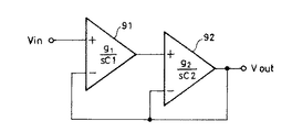
例えば図9は、バイクワッド回路と呼ばれるインダクタンス成分を形成するための回路の構成を示す。
【0004】
この回路において、2つの演算増幅器91、92が従属に設けられる。そして入力信号Vinが演算増幅器91の非反転入力に供給され、この演算増幅器91の出力が演算増幅器92の非反転入力に供給され、この演算増幅器92の出力信号Vout が取り出されると共に、この出力信号Vout が演算増幅器91、92の反転入力に帰還される。従ってこの回路において、演算増幅器91、92の2組の積分器によって構成する帰還回路によりインダクタンス成分が形成される。
【0005】
しかしながらこの回路においては、回路的に電圧帰還が掛かるために、いわゆるQの高いフィルター回路を形成する場合に、入力と出力とでオフセット電圧が生じ、回路設計が極めて困難になるものである。またこの回路の場合に、積分器の入出力はシングルであるために、回路全体もシングル入力のシングル出力となり、差動性に欠けるものとなる。このことは、特に回路のIC化を行う場合には致命的な欠陥であった。
【0006】
すなわち上述の回路においては、インダクタンス成分を単独でIC回路内に形成することができず、このため特に急峻なカットオフ特性を示すチェビシュフ型などの分布定数型のフィルターを組むことができないのである。
【0007】
この出願はこのような点に鑑みて成されたものであって、解決しようとする問題点は、従来の回路では、インダクタンス成分をIC回路内に単独の2端子素子として形成することができなかったというものである。
【0008】
【課題を解決するための手段】
このため本発明の請求項1においては、90度移相器の出力電圧を一組の差動対を介して電流に変換し、この電流を90度移相器の入力側に戻すようにしたものであって、これによれば、シングル入力時に完全な2端子のインダクタンス成分として動作させることができる。
【0009】
また、本発明の請求項3においては、90度移相器の出力電圧を2組の差動対で受け、その一方を電流に変換して90度移相器の入力側に戻すと共に、他方の出力を抵抗マトリクスを介して出力側に電圧帰還するようにしたものであって、これによれば、差動入力、差動出力の形態を持った4端子のインダクタンス回路を形成することができる。
【0010】
さらに本発明の請求項2、4においては、上述の請求項1、3のアクティブインダクタンス回路に電流可変回路を挿入することにより、得られるインダクタンスの値を可変とすることができる。
【0011】
【発明の実施の形態】
すなわち本発明の請求項1においては、正抵抗に対して負性抵抗を帰還したハイインピーダンス回路のハイインピーダンス部分に容量を付加することにより形成した差動型の90度移相器を有し、90度移相器の出力電圧を一組の差動対で受け、この差動対のエミッタ間抵抗により電圧−電流変換し、この電流を90度移相器の入力側に戻すことにより、90度移相器の入力側からみたインピーダンスを2端子のインダクタンスとして作用させるものである。
【0012】
また本発明の請求項2は、請求項1において差動対の電圧−電流変換部に電流可変回路を挿入することによりインダクタンスの値を可変とするものである。
【0013】
さらに本発明の請求項3においては、正抵抗に対して負性抵抗を帰還したハイインピーダンス回路のハイインピーダンス部分に容量を付加することにより形成した差動型の90度移相器を有し、90度移相器の出力電圧を第1及び第2の差動対で受け、この第1の差動対のエミッタ間抵抗により電圧−電流変換し、この電流を90度移相器の入力側に戻すと共に、この第2の差動対の出力部分をトランジスタのベースで受けて、90度移相器の出力側に抵抗を介して電圧帰還することにより、90度移相器の入力側からみたインピーダンスを差動入力及び差動出力の形態を持った4端子のインダクタンスとして作用させるものである。
【0014】
また本発明の請求項4は、請求項3において第1の差動対の電圧−電流変換部及び第2の差動対の出力部分にそれぞれ電流可変回路を挿入することによりインダクタンスの値を可変とするものである。
【0015】
ところで本願発明者は、先に負性抵抗を用いたハイインピーダンスバイアス回路にコンデンサを付加して構成した90度移相器を提案した(特願平9−237162号参照)。本発明のアクティブインダクタンス回路は、この90度移相器を応用したものである。
【0016】
【実施例】
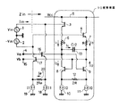
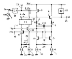
以下、図面を参照して本発明を説明するに、図1は本発明の請求項1によるアクティブインダクタンス回路の一例の構成を示す接続図である。
【0017】
この図1において、差動の入力信号Vinと−Vinを形成する信号源電圧源1、2が設けられ、これらの電圧源1、2の一端が互いに接続されてその接続中点が接地されると共に、信号源電圧源1、2の他端がそれぞれトランジスタ3、4のベースに接続される。さらにこれらのトランジスタ3、4のコレクタが電源Vccの電源路5に接続される。
【0018】
また、これらのトランジスタ3、4のエミッタが、それぞれ抵抗値Rの抵抗器6、7を通じて差動対を構成するトランジスタ8、9のコレクタに接続される。さらにこれらのトランジスタ8、9のエミッタがそれぞれ電流値I0 の電流源10、11を通じて接地されると共に、これらのトランジスタ8、9のエミッタ間に抵抗値2Rの抵抗器12が接続される。そしてこれらのトランジスタ8、9のコレクタ間に容量値C/2のコンデンサ13が接続される。
【0019】
さらにこれらのトランジスタ8、9のコレクタから出力信号Va とVb の出力端子14、15が導出される。
【0020】
また、これらの出力端子14、15がそれぞれトランジスタ16、17のベースに接続される。さらにこれらのトランジスタ16、17のエミッタがそれぞれ電流値I1 の電流源18、19を通じて接地されると共に、これらのトランジスタ16、17のエミッタ間に抵抗値2Re の抵抗器20が接続される。そしてこれらのトランジスタ16、17のコレクタが、それぞれ信号源電圧源1、2とトランジスタ3、4のベースの接続中点に接続される。
【0021】
この図1の回路において、線で囲った部分は90度移相器である。ただし上述の先願では、この90度移相器を電流ドライブとしたが、図1では電圧ドライブに構成している。
【0022】
そこでこの90度移相器において、各部の電流を図示のように値i1 、i2 、i3 、ic に定めると、トランジスタ3側では、i1 =ic +i2 から、
【数1】

【0023】
同様に、トランジスタ4側では、i3 =−ic +i2 から、
【数2】
【0024】
そこで〔数1〕〔数2〕から、これらを加算して
【数3】
【0025】
そこでこの〔数3〕を〔数1〕に代入することによって、
【数4】
【0026】
よって、
【数5】
【0027】
そこで図1の回路において、入力信号Vinの信号源電圧源1からみた入力インピーダンスを値Zinとすると、入力電流Iinは、
【数6】
【0028】
よって、この〔数6〕と上述の〔数4〕とから
【数7】
【0029】
すなわちこの図1の回路において、入力インピーダンスZinは、〔数7〕から明らかなように入力信号Vinに対してインダクタンスL=C・R・Re が対接地間に入っているように見えるものである。言い換えると、入力信号Vin、−Vinの信号源電圧源1、2間に、インダクタンス2L=2・C・R・Re が存在しているように見えるものである。
【0030】
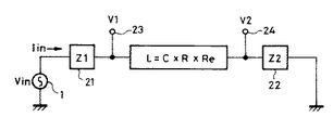
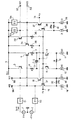
さらに、図1のアクティブインダクタンス回路が完全に2端子素子として存在していることを図2を用いて説明する。この図2は、入力信号Vinの信号源電圧源1とトランジスタ3のベースとの間に値Z1 のドライブインピーダンス21を挿入すると共に、トランジスタ4のベースを値Z2 のインピーダンス22にて終端したものである。
【0031】
そしてこの図2の回路において、トランジスタ3のベースポイント23の信号電位を値V1 、トランジスタ4のベースポイント24の信号電位を値V2 としたときに、値V1 、V2 間にインダクタンスが存在するように伝達関数が表されればよいことになる。
【0032】
そこで図2において、上述の〔数1〕から、
【数8】
【0033】
同様に、〔数2〕から、
【数9】
【0034】
従って、これらの〔数8〕〔数9〕から、
【数10】
【0035】
また、
【数11】
【数12】
【0036】
一方、
【数13】
【数14】
【0037】
すなわち
【数15】
【数16】
【数17】
【0038】
そしてこれらの式より、
【数18】
【0039】
すなわち、これらの〔数18〕から明らかなように、電圧値V1 、V2 は入力信号Vinに対して同一の分母で表され、さらに入力信号Vinに対してインピーダンスの順序もZ1 、L=C・R・Re 、Z2 となっている。以上のことから、上述の図1で形成されるアクティブインダクタンス回路は、完全に2端子素子として浮いた状態で形成されることがわかるものである。なお図3には、2端子素子としてのイメージを上述の図2の回路について示す。
【0040】
従ってこの装置において、90度移相器の出力電圧を一組の差動対を介して電流に変換し、この電流を90度移相器の入力側に戻すことによって、シングル入力時に完全な2端子のインダクタンス成分として動作させることができる。
【0041】
これによって、従来の回路では、インダクタンス成分をIC回路内に単独の2端子素子として形成することができなかったものを、本発明によればこの問題点を容易に解消することができるものである。
【0042】
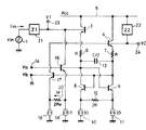
さらに、図4は本発明の請求項3によるアクティブインダクタンス回路の一例の構成を示す接続図である。
【0043】
この図4において、第2の差動の入力信号V2 と−V2 を形成する信号源電圧源31、32が設けられ、これらの電圧源31、32の一端が互いに接続されてその接続中点が接地されると共に、信号源電圧源31、32の他端がそれぞれトランジスタ33、34のベースに接続される。さらにこれらのトランジスタ33、34のコレクタが電源Vccの電源路5に接続される。そしてこれらのトランジスタ33、34のエミッタが、それぞれ抵抗値Rの抵抗器35、36を通じてトランジスタ8、9のベースに接続される。
【0044】
また出力信号Va とVb の出力端子14、15がそれぞれトランジスタ37、38のベースに接続される。さらにこれらのトランジスタ37、38のエミッタがそれぞれ電流値I1 の電流源39、40を通じて接地されると共に、これらのトランジスタ37、38のエミッタ間に抵抗値2Rp の抵抗器41が接続される。そしてこれらのトランジスタ37、38のコレクタが、それぞれ信号源電圧源31、32とトランジスタ33、34のベースの接続中点に接続される。
【0045】
なお図4において、この他の構成は上述の図1と同様とし、対応する部分には同一の符号を付して示す。ただし図4においては、説明の都合上、信号源電圧源1、2で形成される差動の入力信号を値V1 と−V1 とし、抵抗器12の抵抗値を2Rx とする。
【0046】
すなわちこの回路は、上述の図1に示したアクティブインダクタンス回路に、出力側の電圧を帰還する抵抗マトリクスを形成する部分と、電流出力を形成する差動対を追加したものである。そこでこの図4の回路において、信号源電圧源1から供給される入力電流を値Iin1 、信号源電圧源31から供給される入力電流を値Iin2 と置いて、入力電圧V1 、V2 間のインピーダンスを求める。
【0047】
ここで
【数19】
【数20】
【0048】
従って、
【数21】
【数22】
【0049】
そこで入力電圧V1 、V2 間のインピーダンスを値Z12とすると、
【数23】
【0050】
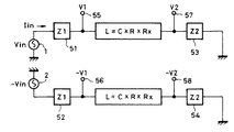
さらに、図4のアクティブインダクタンス回路が完全に2端子対(差動4端子)素子として存在していることを図5を用いて説明する。この図5は、入力信号V1 と−V1 の信号源電圧源1、2とトランジスタ3、4のベースとの間に、それぞれ値Z1 のドライブインピーダンス51、52を挿入すると共に、トランジスタ33、34のベースをそれぞれ値Z2 のインピーダンス53、54にて終端したものである。
【0051】
そしてこの図5の回路において、それぞれのトランジスタ3のベースポイント55の信号電位を値V11、トランジスタ4のベースポイント56の信号電位を値V12、トランジスタ33のベースポイント57の信号電位を値V21、トランジスタ34のベースポイント58の信号電位を値V22としたときに、値V11、V12、V21、V22間にインダクタンスが存在するように伝達関数が表されればよいことになる。なおこの図5の回路において、トランジスタ8、9のエミッタ抵抗は、上述の条件に従ってRになっている。
【0052】
そこで上述の〔数20〕から、
【数24】
【0053】
従って、この〔数24〕から、
【数25】
【0054】
また、
【数26】
【数27】
【0055】
また、
【数28】
【数29】
【0056】
次に、
【数30】
【数31】
【0057】
また、
【数32】
【数33】
【0058】
よって、
【数34】
【0059】
さらに〔数27〕から、
【数35】
【0060】
従って
【数36】
また、〔数29〕から、
【数37】
【0062】
すなわち、これらの〔数36〕〔数37〕から明らかなように、電圧値V11、V21は入力信号Vinに対して同一の分母で表され、さらに入力信号Vinに対してインピーダンスの順序もZ1 、L=C・R・Rp 、Z2 となっている。これは、電圧値V12、V22に対しても同様に表される。以上のことから、上述の図4で形成されるアクティブインダクタンス回路は、完全に2端子対(差動4端子)素子として浮いた状態で形成されることがわかるものである。なお図6には、2端子対素子としてのイメージを上述の図5の回路について示す。
【0063】
従ってこの装置において、90度移相器の出力電圧を2組の差動対で受け、その一方を電流に変換して90度移相器の入力側に戻すと共に、他方の出力を抵抗マトリクスを介して出力側に電圧帰還することによって、差動入力、差動出力の形態を持った4端子のインダクタンス回路を形成することができる。
【0064】
さらに図7、図8には電流可変回路を用いて、上述のアクティブインダクタンス回路のインダクタンス値を可変とするものである。すなわち図7においては、例えば上述の図2の回路についてトランジスタ16、17のコレクタに、k倍(kは+1から−1まで可変可能)の電流可変回路61を挿入する。
【0065】
この回路において、
【数38】
【数39】
【0066】
従って、
【数40】
【0067】
これによって、端子23、24間に存在するインダクタンス値L1 は、
【数41】
【0068】
同様にして、図8においては、例えば上述の図5の回路についてトランジスタ16、17、37、38のコレクタに、それぞれk倍(kは+1から−1まで可変可能)の電流可変回路61、62を挿入する。これによって、端子55、56、57、58間に存在するインダクタンス値L2 は、
【数42】
【0069】
従ってこの装置において、上述のアクティブインダクタンス回路に電流可変回路を挿入することにより、得られるインダクタンスの値を可変とすることができる。
【0070】
こうして上述のアクティブインダクタンス回路によれば、正抵抗に対して負性抵抗を帰還したハイインピーダンス回路のハイインピーダンス部分に容量を付加することにより形成した差動型の90度移相器を有し、90度移相器の出力電圧を一組の差動対で受け、この差動対のエミッタ間抵抗により電圧−電流変換し、この電流を90度移相器の入力側に戻すことにより、90度移相器の入力側からみたインピーダンスを2端子のインダクタンスとして作用させるものである。
【0071】
また、上述の回路において、差動対の電圧−電流変換部に電流可変回路を挿入することによりインダクタンスの値を可変とするものである。
【0072】
さらに上述のアクティブインダクタンス回路によれば、正抵抗に対して負性抵抗を帰還したハイインピーダンス回路のハイインピーダンス部分に容量を付加することにより形成した差動型の90度移相器を有し、90度移相器の出力電圧を第1及び第2の差動対で受け、この第1の差動対のエミッタ間抵抗により電圧−電流変換し、この電流を90度移相器の入力側に戻すと共に、この第2の差動対の出力部分をトランジスタのベースで受けて、90度移相器の出力側に抵抗マトリクスを用いて電圧帰還することにより、90度移相器の入力側からみたインピーダンスを差動入力及び差動出力の形態を持った4端子のインダクタンスとして作用させるものである。
【0073】
また、上述の回路において、第1の差動対の電圧−電流変換部及び第2の差動対の出力部分にそれぞれ電流可変回路を挿入することによりインダクタンスの値を可変とするものである。
【0074】
すなわち本発明のアクティブインダクタンス回路によれば、従来、単独でIC回路内に作ることが困難であったインダクタンス素子を、完全な2端子素子として作りだすことができる。従ってその2端子素子となったインダクタンスの前後にドライブインピーダンスと終端インピーダンスを置けることになり、分布定数回路の選択特性の実現が可能となり、急峻な特性を得ることができる。
【0075】
また、このインダクタンスを完全な4端子対とすることにより、差動入力、差動出力のフィルターを完成することができ、これにより従来のアクティブフィルターで問題であった入力と出力のDCオフセットが完全になくなり、高いQのアクティブフィルターを作ることが可能になる。
【0076】
また差動であるため、従来のアクティブフィルターでは信号電流がアースを回って回路に影響を与える恐れがあったが、本発明の回路によれば差動とすることにより全ての信号がIC回路内にとどまり、回路の性能を向上させることができる。さらに本発明の回路によれば、PNPトランジスタを使用しないので、低電圧に充分対応できる。
【0077】
また、全て差動で信号が流れるため、IC内に使用するコンデンサを全て差動的に付加することができ、シングル動作時に比して半分の容量値で済むことになり、ICチップの面積を大幅に縮小することができる。
【0078】
従ってこれらの理由により、結果として商品の性能向上、製造コストの削減、基板面積の縮小等の効果をもたらすことができる。
【0079】
さらにアクティブインダクタンスを作りだすことによって、例えば位相ロックループや、AM復調器、FM復調器、フィルター等の用途にも本発明を応用することができるものである。
【0080】
【発明の効果】
従って本発明の請求項1によれば、正抵抗に対して負性抵抗を帰還したハイインピーダンス回路のハイインピーダンス部分に容量を付加することにより形成した差動型の90度移相器を有し、90度移相器の出力電圧を一組の差動対で受け、この差動対のエミッタ間抵抗により電圧−電流変換し、この電流を90度移相器の入力側に戻すことにより、90度移相器の入力側からみたインピーダンスを2端子のインダクタンスとして作用させることができるものである。
【0081】
また、本発明の請求項3によれば、90度移相器の出力電圧を2組の差動対で受け、その一方を電流に変換して90度移相器の入力側に戻すと共に、他方の出力を抵抗マトリクスを介して出力側に電圧帰還することによって、差動入力、差動出力の形態を持った4端子のインダクタンス回路を形成することができるものである。
【0082】
さらに本発明の請求項2、4によれば、上述のアクティブインダクタンス回路に電流可変回路を挿入することにより、得られるインダクタンスの値を可変とすることができるものである。
【図面の簡単な説明】
【図1】本発明の請求項1のアクティブインダクタンス回路の一例の構成図である。
【図2】その説明のための図である。
【図3】その説明のための図である。
【図4】本発明の請求項3のアクティブインダクタンス回路の一例の構成図である。
【図5】その説明のための図である。
【図6】その説明のための図である。
【図7】本発明の請求項2のアクティブインダクタンス回路の一例の構成図である。
【図8】本発明の請求項4のアクティブインダクタンス回路の一例の構成図である。
【図9】従来の回路の説明のための図である。
【符号の説明】
1,2…差動の入力電圧Vinと−Vinを形成する信号源電圧源、3,4…電圧ドライブを行うトランジスタ、5…電源Vccの電源路、6,7…抵抗値2Re の抵抗器、8,9…差動対を構成するトランジスタ、10,11…電流値I0 の電流源、12…抵抗値2Rの抵抗器、13…容量値C/2のコンデンサ、14,15…出力電圧Va とVb の出力端子、16,17…トランジスタ、18,19…電流値I1 の電流源、20…抵抗値2Re の抵抗器[0001]
BACKGROUND OF THE INVENTION
The present invention relates to an active inductance circuit suitable for use in a radio receiver, a television receiver, a satellite broadcast receiver, a video tape recorder (VTR), a mobile communication device, and the like.
[0002]
[Prior art]
In devices such as a radio receiver, a television receiver, a satellite broadcast receiver, a video tape recorder (VTR), and a mobile communication device, a filter circuit is used as a part of the circuit configuration. Therefore, when such a filter circuit is constructed in an integrated circuit (IC), for example, a resistor or a capacitor can be conventionally formed of a two-terminal element, but a so-called inductance component is included in the IC. It was not easy to form with two terminals.
[0003]
[Problems to be solved by the invention]
For example, FIG. 9 shows a configuration of a circuit for forming an inductance component called a biquad circuit.
[0004]
In this circuit, two
[0005]
However, in this circuit, since voltage feedback is applied in terms of circuit, when a so-called high-Q filter circuit is formed, an offset voltage is generated between the input and the output, and circuit design becomes extremely difficult. In the case of this circuit, since the input / output of the integrator is single, the entire circuit also becomes a single input with a single input and lacks differential characteristics. This is a fatal defect particularly when the circuit is made into an IC.
[0006]
That is, in the circuit described above, the inductance component cannot be formed alone in the IC circuit, and therefore, a Chebyshoff type distributed constant type filter exhibiting a particularly steep cutoff characteristic cannot be assembled.
[0007]
This application has been made in view of the above points, and the problem to be solved is that in the conventional circuit, the inductance component cannot be formed as a single two-terminal element in the IC circuit. It is something that.
[0008]
[Means for Solving the Problems]
For this reason, in
[0009]
Further, in
[0010]
Further, in the second and fourth aspects of the present invention, the inductance value obtained can be made variable by inserting a current variable circuit into the active inductance circuit of the first and third aspects.
[0011]
DETAILED DESCRIPTION OF THE INVENTION
That is, in
[0012]
According to a second aspect of the present invention, the inductance value is made variable by inserting a current variable circuit into the voltage-current conversion section of the differential pair.
[0013]
Furthermore, in
[0014]
According to a fourth aspect of the present invention, the inductance value can be varied by inserting a current variable circuit in each of the voltage-current conversion section of the first differential pair and the output section of the second differential pair in the third aspect. It is what.
[0015]
Incidentally, the inventor of the present application has previously proposed a 90-degree phase shifter configured by adding a capacitor to a high impedance bias circuit using a negative resistance (see Japanese Patent Application No. 9-237162). The active inductance circuit of the present invention is an application of this 90 degree phase shifter.
[0016]
【Example】
Hereinafter, the present invention will be described with reference to the drawings. FIG. 1 is a connection diagram showing an example of the configuration of an active inductance circuit according to
[0017]
In FIG. 1, signal
[0018]
The emitters of these
[0019]
Further,
[0020]
These
[0021]
In the circuit of FIG. 1, the portion enclosed by a line is a 90 degree phase shifter. However, in the above-mentioned prior application, this 90-degree phase shifter is a current drive, but in FIG. 1, it is configured as a voltage drive.
[0022]
Therefore, in this 90-degree phase shifter, if the current of each part is determined to the values i1, i2, i3, ic as shown in the figure, on the
[Expression 1]
[0023]
Similarly, on the
[Expression 2]
[0024]
From [Equation 1] and [Equation 2], add these together to obtain [Equation 3].
[0025]
Therefore, by substituting [Equation 3] into [Equation 1],
[Expression 4]
[0026]
Therefore,
[Equation 5]
[0027]
Therefore, in the circuit of FIG. 1, when the input impedance of the input signal Vin viewed from the signal
[Formula 6]
[0028]
Therefore, from this [Equation 6] and the above [Equation 4],
[0029]
In other words, in the circuit of FIG. 1, the input impedance Zin appears to have an inductance L = C · R · Re between the ground with respect to the input signal Vin as apparent from [Equation 7]. . In other words, it appears that an inductance 2L = 2 · C · R · Re exists between the signal
[0030]
Further, the fact that the active inductance circuit of FIG. 1 exists as a two-terminal element will be described with reference to FIG. In FIG. 2, a
[0031]
In the circuit of FIG. 2, when the signal potential at the
[0032]
In FIG. 2, from the above [Equation 1],
[Equation 8]
[0033]
Similarly, from [Equation 2],
[Equation 9]
[0034]
Therefore, from these [Equation 8] and [Equation 9],
[Expression 10]
[0035]
Also,
## EQU11 ##
[Expression 12]
[0036]
on the other hand,
[Formula 13]
[Expression 14]
[0037]
That is, [Expression 15]
[Expression 16]
[Expression 17]
[0038]
And from these equations,
[Formula 18]
[0039]
In other words, these [Equation 18] or al apparent, the voltage value V1, V2 are represented by the same denominator with respect to the input signal Vin, also the order of the impedance to further input signal Vin Z1, L = C・ R ・ Re, Z2. From the above, it can be seen that the above-described active inductance circuit formed in FIG. 1 is completely formed as a two-terminal element. FIG. 3 shows an image as a two-terminal element for the circuit of FIG.
[0040]
Therefore, in this device, the output voltage of the 90-degree phase shifter is converted into a current through a pair of differential pairs, and this current is returned to the input side of the 90-degree phase shifter, so that a complete 2 at the time of single input is obtained. It can be operated as an inductance component of the terminal.
[0041]
As a result, according to the present invention, this problem can be easily solved by the conventional circuit in which the inductance component cannot be formed as a single two-terminal element in the IC circuit. .
[0042]
FIG. 4 is a connection diagram showing an example of the configuration of an active inductance circuit according to
[0043]
In FIG. 4, signal
[0044]
The
[0045]
In FIG. 4, other configurations are the same as those in FIG. 1 described above, and corresponding portions are denoted by the same reference numerals. However, in FIG. 4, for the convenience of explanation, the differential input signals formed by the signal
[0046]
That is, this circuit is obtained by adding a portion for forming a resistance matrix for feeding back the voltage on the output side and a differential pair for forming a current output to the active inductance circuit shown in FIG. Therefore, in the circuit of FIG. 4, the input current supplied from the signal
[0047]
Where [Equation 19]
[Expression 20]
[0048]
Therefore,
[Expression 21]
[Expression 22]
[0049]
Therefore, if the impedance between the input voltages V1 and V2 is Z12,
[Expression 23]
[0050]
Further, it will be described with reference to FIG. 5 that the active inductance circuit of FIG. 4 is completely present as a two-terminal pair (differential four-terminal) element. FIG. 5 shows that drive
[0051]
In the circuit of FIG. 5, the signal potential of the
[0052]
Therefore, from the above [Equation 20],
[Expression 24]
[0053]
Therefore, from this [Equation 24],
[Expression 25]
[0054]
Also,
[Equation 26]
[Expression 27]
[0055]
Also,
[Expression 28]
[Expression 29]
[0056]
next,
[30]
[31]
[0057]
Also,
[Expression 32]
[Expression 33]
[0058]
Therefore,
[Expression 34]
[0059]
Furthermore, from [Equation 27],
[Expression 35]
[0060]
Therefore,
From [Equation 29],
[Expression 37]
[0062]
That is, as apparent from these [Equation 36] and [Equation 37], the voltage values V11 and V21 are expressed by the same denominator with respect to the input signal Vin, and the impedance order with respect to the input signal Vin is also Z1,. L = C.R.Rp, Z2. This is similarly expressed for the voltage values V12 and V22. From the above, it can be seen that the active inductance circuit formed in FIG. 4 described above is completely formed in a floating state as a two-terminal pair (differential four-terminal) element. FIG. 6 shows an image as a two-terminal pair element for the circuit of FIG.
[0063]
Therefore, in this device, the output voltage of the 90-degree phase shifter is received by two sets of differential pairs, one of which is converted into a current and returned to the input side of the 90-degree phase shifter, and the other output is connected to the resistance matrix. Thus, a four-terminal inductance circuit having a differential input and differential output configuration can be formed by voltage feedback to the output side.
[0064]
Further, in FIGS. 7 and 8, a current variable circuit is used to vary the inductance value of the above-described active inductance circuit. That is, in FIG. 7, for example, in the circuit of FIG.
[0065]
In this circuit,
[Formula 38]
[39]
[0066]
Therefore,
[Formula 40]
[0067]
As a result, the inductance value L1 existing between the
[Expression 41]
[0068]
Similarly, in FIG. 8, for example, in the circuit of FIG. 5 described above, the current
[Expression 42]
[0069]
Accordingly, in this apparatus, the inductance value obtained can be made variable by inserting a current variable circuit into the above-described active inductance circuit.
[0070]
Thus, according to the above-described active inductance circuit, it has a differential 90 degree phase shifter formed by adding a capacitor to the high impedance portion of the high impedance circuit in which a negative resistance is fed back with respect to a positive resistance, The output voltage of the 90-degree phase shifter is received by a pair of differential pairs, voltage-to-current conversion is performed by the resistance between the emitters of the differential pair, and this current is returned to the input side of the 90-degree phase shifter. The impedance viewed from the input side of the phase shifter acts as an inductance of two terminals.
[0071]
In the above-described circuit, the inductance value is made variable by inserting a current variable circuit in the voltage-current converter of the differential pair.
[0072]
Furthermore, according to the above-described active inductance circuit, it has a differential 90 degree phase shifter formed by adding a capacitor to the high impedance part of the high impedance circuit in which a negative resistance is fed back with respect to a positive resistance, The output voltage of the 90-degree phase shifter is received by the first and second differential pairs, and voltage-current conversion is performed by the resistance between the emitters of the first differential pair, and this current is input to the input side of the 90-degree phase shifter. And receiving the output portion of the second differential pair at the base of the transistor, and feeding back the voltage to the output side of the 90-degree phase shifter using a resistance matrix, thereby providing an input side of the 90-degree phase shifter. The impedance seen from the above is made to act as an inductance of four terminals having a form of differential input and differential output.
[0073]
Further, in the above-described circuit, the value of inductance is made variable by inserting a current variable circuit into the voltage-current converter of the first differential pair and the output part of the second differential pair, respectively.
[0074]
That is, according to the active inductance circuit of the present invention, it is possible to produce an inductance element that has heretofore been difficult to make alone in an IC circuit as a complete two-terminal element. Therefore, the drive impedance and the termination impedance can be placed before and after the inductance that becomes the two-terminal element, so that the selection characteristic of the distributed constant circuit can be realized, and a steep characteristic can be obtained.
[0075]
In addition, by making this inductance into a complete four-terminal pair, a filter with differential input and differential output can be completed, which makes it possible to completely eliminate the DC offset between input and output, which was a problem with conventional active filters. This makes it possible to make an active filter with a high Q.
[0076]
In addition, because of the differential, in the conventional active filter, there is a risk that the signal current may go around the ground and affect the circuit. However, according to the circuit of the present invention, all signals are placed in the IC circuit. The circuit performance can be improved. Furthermore, according to the circuit of the present invention, since no PNP transistor is used, it can sufficiently cope with a low voltage.
[0077]
In addition, since all the signals flow differentially, all the capacitors used in the IC can be added differentially, which means that the capacitance value can be reduced by half compared to the single operation, and the area of the IC chip can be reduced. It can be greatly reduced.
[0078]
Therefore, for these reasons, as a result, effects such as improvement in product performance, reduction in manufacturing cost, reduction in substrate area, and the like can be brought about.
[0079]
Further, by creating an active inductance, the present invention can be applied to uses such as a phase lock loop, an AM demodulator, an FM demodulator, and a filter.
[0080]
【The invention's effect】
Therefore, according to the first aspect of the present invention, the differential 90 degree phase shifter formed by adding a capacitor to the high impedance portion of the high impedance circuit in which the negative resistance is fed back with respect to the positive resistance is provided. The output voltage of the 90-degree phase shifter is received by a pair of differential pairs, voltage-current conversion is performed by the resistance between the emitters of the differential pair, and this current is returned to the input side of the 90-degree phase shifter. The impedance viewed from the input side of the 90 degree phase shifter can act as an inductance of two terminals.
[0081]
According to
[0082]
Further, according to the second and fourth aspects of the present invention, the inductance value obtained can be made variable by inserting a current variable circuit into the above-described active inductance circuit.
[Brief description of the drawings]
1 is a configuration diagram of an example of an active inductance circuit according to
FIG. 2 is a diagram for explaining that;
FIG. 3 is a diagram for explaining that;
FIG. 4 is a configuration diagram of an example of an active inductance circuit according to
FIG. 5 is a diagram for explaining that;
FIG. 6 is a diagram for explaining that;
FIG. 7 is a configuration diagram of an example of an active inductance circuit according to
FIG. 8 is a configuration diagram of an example of an active inductance circuit according to
FIG. 9 is a diagram for explaining a conventional circuit;
[Explanation of symbols]
1, 2... Signal source voltage source for forming differential input voltages Vin and −Vin, 3, 4... Transistor for driving voltage, 5... Power supply path of power supply Vcc, 6, 7. 8, 9 ... Transistors constituting a differential pair, 10, 11 ... Current source of current value I0, 12 ... Resistor with
Claims (4)
上記90度移相器の出力電圧を一組の差動対で受け、この差動対のエミッタ間抵抗により電圧−電流変換し、この電流を上記90度移相器の入力側に戻すことにより、
上記90度移相器の入力側からみたインピーダンスを2端子のインダクタンスとして作用させる
ことを特徴とするアクティブインダクタンス回路。A differential 90 degree phase shifter formed by adding a capacitor to the high impedance part of the high impedance circuit that feeds back the negative resistance with respect to the positive resistance;
The output voltage of the 90-degree phase shifter is received by a pair of differential pairs, voltage-current conversion is performed by the resistance between the emitters of the differential pair, and this current is returned to the input side of the 90-degree phase shifter. ,
An active inductance circuit characterized in that an impedance viewed from the input side of the 90-degree phase shifter acts as an inductance of two terminals.
上記差動対の電圧−電流変換部に電流可変回路を挿入することにより上記インダクタンスの値を可変とする
ことを特徴とするアクティブインダクタンス回路。The active inductance circuit according to claim 1,
An active inductance circuit characterized in that the value of the inductance is made variable by inserting a current variable circuit in the voltage-current converter of the differential pair.
上記90度移相器の出力電圧を第1及び第2の差動対で受け、この第1の差動対のエミッタ間抵抗により電圧−電流変換し、この電流を上記90度移相器の入力側に戻すと共に、この第2の差動対の出力部分をトランジスタのベースで受けて、上記90度移相器の出力側に抵抗を介して電圧帰還することにより、
上記90度移相器の入力側からみたインピーダンスを差動入力及び差動出力の形態を持った4端子のインダクタンスとして作用させる
ことを特徴とするアクティブインダクタンス回路。A differential 90 degree phase shifter formed by adding a capacitor to the high impedance part of the high impedance circuit that feeds back the negative resistance with respect to the positive resistance;
The output voltage of the 90-degree phase shifter is received by the first and second differential pairs, voltage-to-current conversion is performed by the resistance between the emitters of the first differential pair, and this current is converted to the 90-degree phase shifter. By returning to the input side and receiving the output portion of the second differential pair at the base of the transistor, voltage feedback is made to the output side of the 90-degree phase shifter via a resistor .
An active inductance circuit, wherein the impedance viewed from the input side of the 90-degree phase shifter acts as a four-terminal inductance having a differential input and differential output configuration.
上記第1の差動対の電圧−電流変換部及び上記第2の差動対の出力部分にそれぞれ電流可変回路を挿入することにより上記インダクタンスの値を可変とする
ことを特徴とするアクティブインダクタンス回路。The active inductance circuit according to claim 3, wherein
An active inductance circuit characterized in that the value of the inductance is made variable by inserting a current variable circuit into each of the voltage-current conversion section of the first differential pair and the output section of the second differential pair. .
Priority Applications (1)
| Application Number | Priority Date | Filing Date | Title |
|---|---|---|---|
| JP26026597A JP3736070B2 (en) | 1997-09-25 | 1997-09-25 | Active inductance circuit |
Applications Claiming Priority (1)
| Application Number | Priority Date | Filing Date | Title |
|---|---|---|---|
| JP26026597A JP3736070B2 (en) | 1997-09-25 | 1997-09-25 | Active inductance circuit |
Publications (2)
| Publication Number | Publication Date |
|---|---|
| JPH1197981A JPH1197981A (en) | 1999-04-09 |
| JP3736070B2 true JP3736070B2 (en) | 2006-01-18 |
Family
ID=17345658
Family Applications (1)
| Application Number | Title | Priority Date | Filing Date |
|---|---|---|---|
| JP26026597A Expired - Fee Related JP3736070B2 (en) | 1997-09-25 | 1997-09-25 | Active inductance circuit |
Country Status (1)
| Country | Link |
|---|---|
| JP (1) | JP3736070B2 (en) |
Families Citing this family (1)
| Publication number | Priority date | Publication date | Assignee | Title |
|---|---|---|---|---|
| JP4867352B2 (en) * | 2006-01-10 | 2012-02-01 | ソニー株式会社 | Filter circuit and receiving circuit |
-
1997
- 1997-09-25 JP JP26026597A patent/JP3736070B2/en not_active Expired - Fee Related
Also Published As
| Publication number | Publication date |
|---|---|
| JPH1197981A (en) | 1999-04-09 |
Similar Documents
| Publication | Publication Date | Title |
|---|---|---|
| US5124592A (en) | Active filter | |
| JP2766264B2 (en) | Differential amplifier circuit | |
| JP3361021B2 (en) | Filter circuit | |
| US6476676B1 (en) | Semiconductor integrated circuit | |
| JP3316038B2 (en) | Frequency tuning system for operational transconductance amplifier-capacitor pairs | |
| JPS626722Y2 (en) | ||
| EP0827275B1 (en) | Frequency-dependent resistor | |
| JP3736070B2 (en) | Active inductance circuit | |
| EP0078574B1 (en) | All-pass circuit arrangement | |
| JPH02309710A (en) | Leapfrog filter | |
| EP0410536B1 (en) | Combined current differencing and operational amplifier circuit | |
| JP3700338B2 (en) | 90 degree phase shifter | |
| JP4210873B2 (en) | Impedance conversion circuit, video equipment, audio equipment and communication device | |
| JPH0936702A (en) | Active low-pass filter | |
| JPH0626297B2 (en) | Second-order active phase equalizer | |
| US5302910A (en) | FM detector circuit with error voltage applied to phase shifting circuit | |
| JPH11205085A (en) | Bandpass filter circuit, video equipment, audio equipment, and communication device | |
| JP2962936B2 (en) | Resonance circuit | |
| JPH0114726B2 (en) | ||
| JPH0125040Y2 (en) | ||
| JPH0154884B2 (en) | ||
| JP2000114929A (en) | Impedance circuit and phase shifter | |
| JPH11205084A (en) | High-pass filter circuit, video equipment, audio equipment and communication device | |
| JPH0448019Y2 (en) | ||
| JPH0630415B2 (en) | Differential circuit |
Legal Events
| Date | Code | Title | Description |
|---|---|---|---|
| A621 | Written request for application examination |
Free format text: JAPANESE INTERMEDIATE CODE: A621 Effective date: 20040126 |
|
| A977 | Report on retrieval |
Free format text: JAPANESE INTERMEDIATE CODE: A971007 Effective date: 20050301 |
|
| A131 | Notification of reasons for refusal |
Free format text: JAPANESE INTERMEDIATE CODE: A131 Effective date: 20050621 |
|
| A521 | Written amendment |
Free format text: JAPANESE INTERMEDIATE CODE: A523 Effective date: 20050805 |
|
| TRDD | Decision of grant or rejection written | ||
| A01 | Written decision to grant a patent or to grant a registration (utility model) |
Free format text: JAPANESE INTERMEDIATE CODE: A01 Effective date: 20051004 |
|
| A61 | First payment of annual fees (during grant procedure) |
Free format text: JAPANESE INTERMEDIATE CODE: A61 Effective date: 20051017 |
|
| FPAY | Renewal fee payment (event date is renewal date of database) |
Free format text: PAYMENT UNTIL: 20091104 Year of fee payment: 4 |
|
| LAPS | Cancellation because of no payment of annual fees |