JP3710332B2 - Image forming apparatus - Google Patents
Image forming apparatus Download PDFInfo
- Publication number
- JP3710332B2 JP3710332B2 JP21507899A JP21507899A JP3710332B2 JP 3710332 B2 JP3710332 B2 JP 3710332B2 JP 21507899 A JP21507899 A JP 21507899A JP 21507899 A JP21507899 A JP 21507899A JP 3710332 B2 JP3710332 B2 JP 3710332B2
- Authority
- JP
- Japan
- Prior art keywords
- toner
- image
- charging
- carrier
- forming apparatus
- Prior art date
- Legal status (The legal status is an assumption and is not a legal conclusion. Google has not performed a legal analysis and makes no representation as to the accuracy of the status listed.)
- Expired - Fee Related
Links
- 238000012546 transfer Methods 0.000 claims description 83
- 239000010410 layer Substances 0.000 claims description 35
- 239000006249 magnetic particle Substances 0.000 claims description 31
- 239000000463 material Substances 0.000 claims description 29
- 239000002245 particle Substances 0.000 claims description 22
- 238000004140 cleaning Methods 0.000 claims description 17
- 108091008695 photoreceptors Proteins 0.000 claims description 14
- 229910021417 amorphous silicon Inorganic materials 0.000 claims description 13
- 238000001514 detection method Methods 0.000 claims description 12
- 230000015572 biosynthetic process Effects 0.000 claims description 10
- 239000002344 surface layer Substances 0.000 claims description 6
- 239000002210 silicon-based material Substances 0.000 claims description 2
- 239000002800 charge carrier Substances 0.000 description 92
- 238000000034 method Methods 0.000 description 45
- 238000011161 development Methods 0.000 description 43
- 238000011109 contamination Methods 0.000 description 15
- 230000008569 process Effects 0.000 description 13
- 238000010586 diagram Methods 0.000 description 12
- 238000002347 injection Methods 0.000 description 12
- 239000007924 injection Substances 0.000 description 12
- 238000003860 storage Methods 0.000 description 11
- 239000011347 resin Substances 0.000 description 10
- 230000007246 mechanism Effects 0.000 description 9
- 229920005989 resin Polymers 0.000 description 9
- 239000000654 additive Substances 0.000 description 8
- 230000002093 peripheral effect Effects 0.000 description 8
- 230000007423 decrease Effects 0.000 description 7
- 230000000694 effects Effects 0.000 description 7
- 230000001965 increasing effect Effects 0.000 description 7
- 230000006866 deterioration Effects 0.000 description 6
- 230000001105 regulatory effect Effects 0.000 description 6
- 238000000576 coating method Methods 0.000 description 5
- 238000002156 mixing Methods 0.000 description 5
- 238000011084 recovery Methods 0.000 description 5
- CBENFWSGALASAD-UHFFFAOYSA-N Ozone Chemical compound [O-][O+]=O CBENFWSGALASAD-UHFFFAOYSA-N 0.000 description 4
- 230000000996 additive effect Effects 0.000 description 4
- 239000000356 contaminant Substances 0.000 description 4
- 230000007547 defect Effects 0.000 description 4
- 238000005259 measurement Methods 0.000 description 4
- 230000003287 optical effect Effects 0.000 description 4
- 239000010419 fine particle Substances 0.000 description 3
- 230000005415 magnetization Effects 0.000 description 3
- 229910052751 metal Inorganic materials 0.000 description 3
- 239000002184 metal Substances 0.000 description 3
- VYPSYNLAJGMNEJ-UHFFFAOYSA-N Silicium dioxide Chemical compound O=[Si]=O VYPSYNLAJGMNEJ-UHFFFAOYSA-N 0.000 description 2
- 229910052782 aluminium Inorganic materials 0.000 description 2
- XAGFODPZIPBFFR-UHFFFAOYSA-N aluminium Chemical compound [Al] XAGFODPZIPBFFR-UHFFFAOYSA-N 0.000 description 2
- 230000008859 change Effects 0.000 description 2
- 239000003795 chemical substances by application Substances 0.000 description 2
- 239000011247 coating layer Substances 0.000 description 2
- 230000004927 fusion Effects 0.000 description 2
- 239000000203 mixture Substances 0.000 description 2
- 239000000843 powder Substances 0.000 description 2
- 238000012545 processing Methods 0.000 description 2
- 238000000926 separation method Methods 0.000 description 2
- 238000003756 stirring Methods 0.000 description 2
- 239000004677 Nylon Substances 0.000 description 1
- 239000004698 Polyethylene Substances 0.000 description 1
- GWEVSGVZZGPLCZ-UHFFFAOYSA-N Titan oxide Chemical compound O=[Ti]=O GWEVSGVZZGPLCZ-UHFFFAOYSA-N 0.000 description 1
- 238000009825 accumulation Methods 0.000 description 1
- 229910052787 antimony Inorganic materials 0.000 description 1
- WATWJIUSRGPENY-UHFFFAOYSA-N antimony atom Chemical compound [Sb] WATWJIUSRGPENY-UHFFFAOYSA-N 0.000 description 1
- 230000001174 ascending effect Effects 0.000 description 1
- 230000002238 attenuated effect Effects 0.000 description 1
- 239000011230 binding agent Substances 0.000 description 1
- 239000003990 capacitor Substances 0.000 description 1
- 230000015556 catabolic process Effects 0.000 description 1
- 239000011248 coating agent Substances 0.000 description 1
- 239000011231 conductive filler Substances 0.000 description 1
- 238000002788 crimping Methods 0.000 description 1
- 238000006731 degradation reaction Methods 0.000 description 1
- 230000001419 dependent effect Effects 0.000 description 1
- 125000000664 diazo group Chemical group [N-]=[N+]=[*] 0.000 description 1
- 238000007598 dipping method Methods 0.000 description 1
- 238000007599 discharging Methods 0.000 description 1
- 230000008030 elimination Effects 0.000 description 1
- 238000003379 elimination reaction Methods 0.000 description 1
- 230000002708 enhancing effect Effects 0.000 description 1
- 239000000835 fiber Substances 0.000 description 1
- 239000011521 glass Substances 0.000 description 1
- 150000007857 hydrazones Chemical class 0.000 description 1
- 238000009413 insulation Methods 0.000 description 1
- 239000012212 insulator Substances 0.000 description 1
- 239000004973 liquid crystal related substance Substances 0.000 description 1
- 230000003472 neutralizing effect Effects 0.000 description 1
- 229920001778 nylon Polymers 0.000 description 1
- 230000010355 oscillation Effects 0.000 description 1
- 230000001590 oxidative effect Effects 0.000 description 1
- 239000000049 pigment Substances 0.000 description 1
- 229920005668 polycarbonate resin Polymers 0.000 description 1
- 239000004431 polycarbonate resin Substances 0.000 description 1
- -1 polyethylene Polymers 0.000 description 1
- 229920000573 polyethylene Polymers 0.000 description 1
- 238000003825 pressing Methods 0.000 description 1
- 230000009467 reduction Effects 0.000 description 1
- 230000004044 response Effects 0.000 description 1
- 239000004065 semiconductor Substances 0.000 description 1
- 239000000377 silicon dioxide Substances 0.000 description 1
- 239000000243 solution Substances 0.000 description 1
- 238000005507 spraying Methods 0.000 description 1
- 230000003068 static effect Effects 0.000 description 1
- OGIDPMRJRNCKJF-UHFFFAOYSA-N titanium oxide Inorganic materials [Ti]=O OGIDPMRJRNCKJF-UHFFFAOYSA-N 0.000 description 1
- 230000007704 transition Effects 0.000 description 1
- 239000011882 ultra-fine particle Substances 0.000 description 1
- 238000011144 upstream manufacturing Methods 0.000 description 1
- 229910000859 α-Fe Inorganic materials 0.000 description 1
Images


Classifications
-
- G—PHYSICS
- G03—PHOTOGRAPHY; CINEMATOGRAPHY; ANALOGOUS TECHNIQUES USING WAVES OTHER THAN OPTICAL WAVES; ELECTROGRAPHY; HOLOGRAPHY
- G03G—ELECTROGRAPHY; ELECTROPHOTOGRAPHY; MAGNETOGRAPHY
- G03G15/00—Apparatus for electrographic processes using a charge pattern
- G03G15/02—Apparatus for electrographic processes using a charge pattern for laying down a uniform charge, e.g. for sensitising; Corona discharge devices
- G03G15/0208—Apparatus for electrographic processes using a charge pattern for laying down a uniform charge, e.g. for sensitising; Corona discharge devices by contact, friction or induction, e.g. liquid charging apparatus
- G03G15/0241—Apparatus for electrographic processes using a charge pattern for laying down a uniform charge, e.g. for sensitising; Corona discharge devices by contact, friction or induction, e.g. liquid charging apparatus by bringing charging powder particles into contact with the member to be charged, e.g. by means of a magnetic brush
-
- G—PHYSICS
- G03—PHOTOGRAPHY; CINEMATOGRAPHY; ANALOGOUS TECHNIQUES USING WAVES OTHER THAN OPTICAL WAVES; ELECTROGRAPHY; HOLOGRAPHY
- G03G—ELECTROGRAPHY; ELECTROPHOTOGRAPHY; MAGNETOGRAPHY
- G03G2215/00—Apparatus for electrophotographic processes
- G03G2215/02—Arrangements for laying down a uniform charge
- G03G2215/021—Arrangements for laying down a uniform charge by contact, friction or induction
- G03G2215/022—Arrangements for laying down a uniform charge by contact, friction or induction using a magnetic brush
Landscapes
- Physics & Mathematics (AREA)
- Engineering & Computer Science (AREA)
- Plasma & Fusion (AREA)
- General Physics & Mathematics (AREA)
- Electrostatic Charge, Transfer And Separation In Electrography (AREA)
- Photoreceptors In Electrophotography (AREA)
- Dry Development In Electrophotography (AREA)
- Control Or Security For Electrophotography (AREA)
Description
【0001】
【発明の属する技術分野】
本発明は、転写方式の電子写真装置や静電記録装置などのように、電子写真感光体・静電記録誘電体等の像担持体を所定の極性・電位に一様に帯電し、該像担持体の帯電面に静電潜像を形成し、該静電潜像をトナー像として現像し、該トナー像を転写材に転写し、像担持体は繰り返して作像に使用する画像形成装置に関する。
【0002】
より詳しくは、像担持体を帯電処理する帯電手段として、磁性粒子を用いた接触帯電部材によって像担持体を帯電処理する磁気ブラシ帯電器(磁気ブラシ帯電装置)を用いた画像形成装置に関する。
【0003】
【従来の技術】
図15は画像形成装置の従来例としての転写式電子写真装置(複写機・プリンター・ファクシミリ等)の一例の概略構成図である。
【0004】
111は第1の像担持体としての回転ドラム型の電子写真感光体(以下、感光ドラムと記す)であり、矢印の時計方向に所定の周速度をもって回転駆動される。
【0005】
感光ドラム111はその回転過程において帯電手段112による所定の極性・電位の一様な帯電処理を受ける。帯電手段112は本例では接触帯電部材である帯電ローラである。次いで不図示の像露光手段(原稿画像の投影露光手段、レーザー走査露光手段等)による像露光Lを受ける。これにより、感光ドラム111の一様帯電面が露光像パターンに対応して選択的に除電(あるいは電位減衰)されて、感光ドラム111面に静電潜像が形成される。
【0006】
そしてその静電潜像が現像手段113によりトナー像として現像される。
【0007】
一方、不図示の給紙機構部から第2の像担持体としての転写材(転写紙)Pが感光ドラム111と転写手段114との間の転写部に所定の制御タイミングで給紙されて、感光ドラム111面側のトナー像がこの給紙転写材Pの面に順次に転写されていく。転写手段114は本例では転写ローラである。
【0008】
次いで転写材Pは回転感光体ドラム111面から分離され、不図示の定着手段に導入されてトナー像の定着処理を受けて画像形成物(コピー、プリント)として出力される。
【0009】
転写材Pに対するトナー像転写後の感光ドラム111面はクリーニング装置(クリーナー)115によって転写残りトナーの除去を受けて清掃され、繰り返して作像に供される。
【0010】
1)接触帯電器
上記のような画像形成装置において、感光ドラム111、帯電・露光・現像・転写・クリーニング・定着等の画像形成プロセスの各手段・機器112〜115としては種々の方式・構成のものがある。
【0011】
例えば、感光体ドラム111面を所定の極性・電位に一様に帯電処理する帯電手段112としては、従来一般にコロナ帯電器が使用されてきた。これは、コロナ帯電器を感光ドラムに非接触に対向配設し、高圧を印加したコロナ帯電器から発生するコロナシャワーに感光ドラム表面をさらすことで回転感光ドラム表面を所定の極性・電位に帯電させるものである。
【0012】
近年は、コロナ帯電器よりも低オゾン・低電力等の利点を有することから接触帯電器が実用化されてきている。
【0013】
接触帯電器は、抵抗値調整した導電性部材を接触帯電部材として被帯電体に接触させて配設し、該接触帯電部材に所定の電圧(帯電バイアス)を印加することで、被帯電体表面を所定の極性・電位に帯電させるものである。
【0014】
接触帯電部材としては、導電性ゴムをロール状にしたローラタイプ(帯電ローラ、導電ゴムローラ)、導電性ゴムをブレード状にしたブレードタイプ(帯電ブレード)、磁性粒子を用いた磁気ブラシタイプ、導電性の繊維をブラシ状に形成したファーブラシタイプ等の各種形態のものが好ましく用いられている。
【0015】
磁気ブラシ帯電器は、導電性の磁性粒子を直接にマグネットに、あるいは、マグネットを内包するスリーブ上に磁気ブラシとして磁気的に拘束保持させたものであり、その磁性粒子の磁気ブラシ部を停止あるいは回転させながら被帯電体面に接触させ、これに電圧を印加することによって、被帯電体面を接触帯電させるものであり、帯電・接触の安定性という点から好ましく用いられている。
【0016】
接触帯電部材に印加する帯電バイアスを、直流電圧のみとするDCバイアス印加方式と、直流バイアス成分と交番バイアス成分を有する振動電圧とするACバイアス印加方式がある。
【0017】
2)注入帯電
接触帯電には、特公平3−52058号公報等に開示のように放電現象による帯電が支配的である系と、特開平6−3921号公報等に開示のように被帯電体面に対する電荷の直接注入(充電)による帯電が支配的である系(電荷注入帯電方式)がある。
【0018】
電荷注入帯電方式は、前記のような接触帯電部材を用い、被帯電体として電荷注入帯電性のもの、像担持体の場合は通常の有機感光体上に導電性微粒子を分散させた表層を有するものや、アモルファスシリコン感光体などを用いることで、接触帯電部材に印加したバイアスのうちの直流成分とほぼ同等の帯電電位を被帯電体表面に得ることが可能である。
【0019】
この電荷注入帯電方式は、被体電体への帯電がコロナ帯電器を用いて行われるような放電現象を利用しないので、帯電に必要とされる印加帯電バイアスは所望する被帯電体表面電位分のみであり、オゾンの発生もない完全なオゾンレス、かつ低電力消費型帯電が可能となり、注目されてきている。
【0020】
【発明が解決しようとする課題】
磁気ブラシ接触帯電方式・転写方式の画像形成装置において、画像形成を繰り返すと接触帯電部材である磁気ブラシの磁性粒子の汚染が生じ、帯電性の低下が見られるようになる。
【0021】
磁気ブラシの磁性粒子の汚れの要因は、通常トナー粒子の電気抵抗は比較的高いものが用いられているために磁性粒子に対してトナー粒子の樹脂成分が融着したり、トナー粒子に外添された外添剤が付着することにより発生する。この現象により磁性粒子の抵抗が上昇してしまい、被帯電体である像担持体を所望の電位にまで帯電できなくなったり、帯電ムラが生じたりしてしまい、画像不良が発生してしまう。
【0022】
そこで本発明は特に磁気ブラシ接触帯電方式・転写方式の画像形成装置について、接触帯電部材である磁気ブラシの磁性粒子の汚染による帯電性能の低下を長期にわたって防ぎ、常に良好な画像を維持することを目的とする。
【0023】
【課題を解決するための手段】
本発明は下記の構成を特徴とする画像形成装置である。
【0024】
(1)磁性粒子を用いた接触帯電部材によって像担持体に帯電を施し、該像担持体の帯電面に静電潜像を形成し、該静電潜像をトナー像として現像し、該トナー像を転写材に転写し、像担持体は繰り返して作像に使用する画像形成装置において、トナーの消費量に対応して、磁性粒子が補給されることを特徴とする画像形成装置。
【0025】
(2)トナーの消費量に対応した磁性粒子の補給は、トナー消費量を検知する検知手段の信号に基づくものであることを特徴とする(1)に記載の画像形成装置。
【0026】
(3)トナーの消費量に対応した磁性粒子の補給は、トナー容器内のトナー残量検知手段によるトナー補給タイミングにおいて行われることを特徴とする(1)に記載の画像形成装置。
【0027】
(4)磁性粒子を補給する際は接触帯電部材の使用された磁性粒子の少なくとも一部は剥ぎ取られることを特徴とする(1)ないし(3)の何れかに記載の画像形成装置。
【0028】
(5)像担持体に形成された静電潜像をトナー像として現像する現像手段がトナー像を転写材に転写した後に像担持体に残留した残トナー粒子を回収するクリーニング手段も兼ねることを特徴とする(1)ないし(4)の何れかに記載の画像形成装置。
【0029】
(6)接触帯電部材に印加されるバイアスは、直流バイアスに交番電圧が重畳されたものであることを特徴とする(1)ないし(5)の何れかに記載の画像形成装置。
【0030】
(7)像担持体が表面に109 〜1014Ω・cmの材質からなる層を有することを特徴とする(1)ないし(6)の何れかに記載の画像形成装置。
【0031】
(8)像担持体は、有機感光体表面に109 〜1014Ω・cmの材質からなる表面層を有することを特徴とする(1)ないし(6)の何れかに記載の画像形成装置。
【0032】
(9)像担持体はアモルファスシリコンの材質からなることを特徴とする(1)ないし(6)の何れかに記載の画像形成装置。
【0033】
〈作 用〉
即ち、磁気ブラシ接触帯電方式・転写方式の画像形成装置において、接触帯電部材である磁気ブラシの磁性粒子の汚染度合いが何に依存するかを調べたところ、汚染度合いは耐久の枚数よりもトナーの消費量(使用量)によるものが大きいことがわかってきた。例えば、同じ10000枚の出力によっても画像比率が高い場合と低い場合では大きく汚染状態が違い、画像比率が高い場合には汚染度合いが激しいことが分かった。
【0034】
そこで本発明においては、画像形成過程におけるトナーの消費量に対応して接触帯電部材である磁気ブラシに新しい磁性粒子を補給することにより磁気ブラシをリフレッシュして、磁気ブラシの磁性粒子の汚染による帯電性能の低下を長期にわたって防ぎ、常に良好な画像を維持することを可能とした。
【0035】
【発明の実施の形態】
〈実施例1〉(図1〜図7)
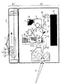
図1は本発明に従う画像形成装置例の概略構成図である。
【0036】
本例の画像形成装置は、転写式電子写真プロセス利用、磁気ブラシ接触帯電方式、LED露光方式、反転現像方式のプリンターである。
【0037】
図1において、Aはプリンター部、Bはその上に搭載設置したイメージリーダー部(画像読取装置)である。
【0038】
(1)イメージリーダー部B
イメージリーダー部Bにおいて、10は固定の原稿台(ガラス等の透明板)であり、この原稿台の上面に原稿Gを複写すべき面を下側にして載置しその上に不図示の原稿圧着板を被せてセットする。
【0039】
9は原稿照射用ランプ9a・短焦点レンズアレイ9b・CCDセンサー9c等を配設した画像読取ユニットである。このユニット9は、コピー開始信号が入力されると、原稿台10の下側において該原稿台の左辺側のホームポジションから右辺側に原稿台下面に沿って往動駆動され、所定の往動終点に達すると復動駆動されて始めのホームポジションに戻される。
【0040】
該ユニット9の往動駆動過程において、原稿台10上の載置セット原稿Gの下向き画像面がユニット9の原稿照射用ランプ9aにより左辺側から右辺側にかけて順次に照明走査され、その照明走査光の原稿面反射光が短焦点レンズアレイ9bによってCCDセンサー9cに結像入射する。
【0041】
CCDセンサー9cは受光部、転送部、出力部より構成されている。CCD受光部において光信号が電荷信号に変えられ、転送部でクロックパルスに同期して順次出力部へ転送され、出力部において電荷信号を電圧信号に変換し、増幅、低インピーダンス化して出力する。このようにして得られたアナログ信号は周知の画像処理がなされてデジタル信号に変換されプリンター部Aに送られる。
【0042】
即ち、イメージリーダー部Bにより原稿Gの画像情報が時系列電気デジタル画素信号(画像信号)として光電読取りされる。
【0043】
(2)プリンター部A
1は第1の像担持体としての回転ドラム型の電子写真感光体(感光ドラム)である。この感光ドラム1は中心支軸を中心に所定の周速度をもって矢示の時計方向aに回転駆動される。本例の感光ドラム1は直径略30mmの電荷注入帯電性・負帯電性の有機感光体であり、周速度100mm/secで回転駆動される。この感光ドラム1の層構成については後述する。
【0044】
a.帯 電:感光ドラム1はその回転過程において帯電手段(帯電装置)としての磁気ブラシ帯電器2によりその外周面が略−650Vに一様に一次帯電処理される。磁気ブラシ帯電器2の構成については後述する。
【0045】
b.露 光:そして該回転感光ドラム1の一様帯電面に対して潜像形成手段(露光手段、露光装置)としてのLED露光器3により画像情報の走査露光がなされて、回転感光ドラム1面にはイメージリーダー部Bにより光電読み取りされた原稿Gの画像情報に対応した静電潜像が順次に形成されていく。
【0046】
すなわち、LED露光器3は感光ドラム1の主走査方向に数多のLEDを配列した発光素子アレーであり、このLED露光器3の個々のLEDの発光がイメージリーダー部B側からプリンター部A側に送られた画像信号に対応して選択的にON・OFF制御され、また感光ドラム1が回転することによる副走査で、回転感光ドラム1面にはLEDの発光による露光部の電位が落ち(明部電位)、非露光部の電位(暗部電位)とのコントラストにより、露光パターンに対応した静電潜像が形成されていく。
【0047】
c.現 像:その回転感光ドラム1面の形成静電潜像が現像手段としての現像器4により順次にトナー像として本例の場合は反転現像されていく。この現像器4の構成については後述する。
【0048】
d.転 写:一方、給紙カセット5内に積載収納されている第2の像担持体としての転写材Pが給紙ローラ5aにより一枚宛繰り出されて給送され、レジストローラ5bにより所定の制御タイミングにて感光ドラム1と転写手段としての転写装置6との接触ニップ部である転写部Tに給紙され、転写材P面に感光ドラム1面側のトナー像が静電転写される。
【0049】
本例における転写装置6はベルト転写装置であり、無端状の転写ベルト6aを駆動ローラ6b及び従動ローラ6c間に懸架し、矢印の反時計方向に感光ドラム1の回転周速度と略同じ周速度で回動駆動させる。無端状転写ベルト6aの内側には転写帯電ブレード6dを備え、このブレード6dでベルト6aの上行側のベルト部分の略中間部を感光ドラム1面に接触させて転写部Tを形成させてある。
【0050】
転写材Pがベルト6aの上行側ベルト部分の上面に乗って転写部Tに搬送される。その搬送転写材Pの先端が転写部Tに進入する時点において転写帯電ブレード6dに不図示の転写バイアス印加電源から所定の転写バイアスが給電されることで転写材Pの裏側からトナーと逆極性の帯電がなされて感光ドラム1上のトナー像が順次に転写材Pの上面に転写されていく。
【0051】
e.定 着: 転写ベルト6aは転写部Tから定着手段としての本例の場合は熱ローラタイプの定着器8への転写材Pの搬送手段を兼ねさせてあり、転写部Tを通過した転写材Pは回転感光ドラム1面から分離されて転写ベルト6で定着器8へ搬送・導入され、トナー像の熱定着を受けてコピーもしくはプリントとして排紙トレイ11に排出される。
【0052】
f.クリーニング:また転写材Pに対するトナー像転写後(転写材分離後)の回転感光ドラム1面はクリーナー(クリーニング装置)7によってドラム面に残留している転写残りトナー等の付着汚染物の除去を受けて清掃されて繰り返して画像形成に使用される。
【0053】
本例のクリーナー7はブレードタイプであり、クリーニングブレード72を感光ドラム1面に所定の押圧力で当接させてこのブレードのエッジ部で回転する感光ドラム1面を拭掃することで感光ドラム1面から転写残りトナー等の付着汚染物を掻き取り除去する。感光ドラム1面から掻き取られた転写残りトナー等の付着汚染物はクリーニング容器71内に収容される。
【0054】
(3)感光ドラム1
第1の像担持体としての感光ドラム1としては、通常用いられている有機感光体等を用いることができるが、望ましくは、有機感光体上にその抵抗が109 〜1014Ω・cmの材質を有する表面層を持つものや、アモルファスシリコン感光体など非晶質のシリコンを有する表面層からなるものを用いると、電荷注入帯電を実現でき、オゾン発生の防止、ならびに消費電力の低減に効果がある。また、帯電性についても向上させることが可能となる。
【0055】
本例における感光ドラム1は電荷注入帯電性・負帯電性の有機感光体であり、図2の層構成模型図のように、直径30mmのアルミニウム製のドラム基体(アルミ基体)1a上に下記の第1〜第5の5つの層1b〜1fを下から順に設けてなるものである。
【0056】
第1層1b;下引き層であり、ドラム基体1aの欠陥等をならすために設けられている厚さ20μmの導電層である。
【0057】
第2層1c;正電荷注入防止層であり、ドラム基体1aから注入された正電荷が感光体表面に帯電された負電荷を打ち消すのを防止する役割を果たし、アミラン樹脂とメトキシメチル化ナイロンによって1×10⁶ Ω・cm程度に抵抗調整された厚さ1μmの中抵抗層である。
【0058】
第3層1d;電荷発生層であり、ジスアゾ系の顔料を樹脂に分散した厚さ約0.3μmの層で露光を受けることによって正負の電荷対を発生する。
【0059】
第4層1e;電荷輸送層であり、ポリカーボネート樹脂にヒドラゾンを分散したものであり、P型半導体である。従って感光体表面に帯電された負電荷はこの層を移動することができず電荷発生層で発生した正電荷のみを感光体表面に輸送することができる。
【0060】
第5層1f;電荷注入層であり、絶縁性樹脂のバインダーに導電性微粒子としてSnO2 超微粒子1gを分散した材料の塗工層である。具体的には絶縁性樹脂に光透過性の導電フィラーであるアンチモンをドーピングして低抵抗化(導電化)した粒径0.03μmのSnO2 粒子を樹脂に対して70重量パーセント分散した材料の塗工層である。このようにして調合した塗工液をディッピング塗工法、スプレー塗工法、ロール塗工法、ビーム塗工法等の適当な塗工法にて厚さ約3μmに塗工して電荷注入層とした。
【0061】
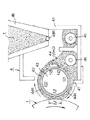
(4)磁気ブラシ帯電器2
図3は磁気ブラシ帯電器2の部分拡大模型図であり、本例のものはスリーブ回転タイプのものである。
【0062】
21は帯電器容器である。
【0063】
22は磁気ブラシ担持部材としての外形16mmの非磁性のスリーブ(以下、帯電スリーブと記す)であり、一部を外部に露呈させて帯電器容器21内に回転可能に配設してある。
【0064】
23は磁界発生手段としてのマグネットローラであり、上記の帯電スリーブ22内に挿入して非回転に固定して配設してあり、この固定のマグネットローラ23の外回りを帯電スリーブ22が、100mm/secの回転速度で回転する感光ドラム1に対してカウンター方向である矢印の時計方向に150mm/secの回転速度で回転駆動される。
【0065】
24は帯電器容器2a内に収容させた帯電用磁性粒子(以下、帯電キャリアと記す)であり、その量は帯電スリーブ22の周面に磁気ブラシとして担持させる量に適当に余裕量を加えた量である。より具体的には本例では帯電スリーブ22の一周分の磁気ブラシの帯電キャリア量よりも多い、40gの帯電キャリアを収容させてある。
【0066】
25は帯電器容器21の開口部に設けた磁気ブラシ層厚規制部材(規制ブレード)であり、帯電スリーブ22に対して所定の僅少な隙間を存して取り付けられている。この規制部材25は、帯電スリーブ22上に該スリーブ内のマグネットローラ23の磁界により磁気ブラシとして磁気拘束されて担持され、帯電スリーブ22の回転に伴い回転搬送されて帯電器容器21内から持ち出される帯電キャリアの量(磁気ブラシの層厚)を所定に規制して適正量の帯電キャリアの磁気ブラシ24aを形成する役目をする。
【0067】
26は帯電スリーブ22に磁気拘束されて担持されている帯電キャリアの磁気ブラシから帯電キャリアを少なくとも一部剥ぎ取る帯電キャリア剥ぎ取り部材である。
【0068】
本例のものは帯電器容器21内においてヒンジ部26aを中心に揺動自在のブレード部材であり、このブレード部材26は例えば電磁ソレノイドやステッピングモータ等の不図示の駆動手段が不図示の制御回路で制御されることで、ブレード先端部が帯電スリーブ22の磁気ブラシ層24aに接触した剥ぎ取り位置と、磁気ブラシ24aから非接触に逃げ離れた退避位置とに転換される。図3の(a)はこの帯電キャリア剥ぎ取り部材としてのブレード部材26が帯電スリーブ22の磁気ブラシ24aから非接触に逃げ離れた退避位置に転換されている状態時を示しており、常時はこの状態が保たれる。(b)はブレード部材26が磁気ブラシ24aに接触した剥ぎ取り位置に転換されている状態時を示している。
【0069】
27は帯電器容器21の上側に設けた帯電キャリア収容室であり、この収容室27内に適当量の補給入れ替え用としての帯電キャリア24を収容させてある。この帯電キャリア収容室27の底部と帯電器容器21の上側とはシャッタ機構部28(図1)を介して連通させてある。シャッタ機構部28は不図示の制御回路により開閉制御される。常時は閉じ状態に保持されて帯電キャリア収容室27から帯電器容器21への帯電キャリアの流れ込みはない。制御回路によりシャッタ機構部28が所定に開き制御されると、帯電キャリア収容室27から帯電器容器21内の帯電スリーブ22上に所定量の帯電キャリアが補給されるようになっている。
【0070】
上記の磁気ブラシ帯電器2の下側にクリーナー7を配設してあり、本例においては磁気ブラシ帯電器2の帯電器容器21とクリーナー7のクリーニング容器71とを上下一連に構成して帯電器容器21とクリーニング容器71とを連通させた形態のものにしてある。taはクリーニングブレード72により感光ドラム1面から掻き落とされてクリーニング容器71内に収容された転写残トナー等の感光ドラム面汚染物である。
【0071】
帯電スリーブ22は感光ドラム1面に対して所定の僅少な隙間を存して対向させてあり、この対向隙間は磁気ブラシ24aの層厚よりも小さくして磁気ブラシ24aを感光ドラム1に接触させて感光ドラム面を磁気ブラシ24aで摺擦するようにしてある。磁気ブラシ24aと感光ドラム1の接触部には磁気ブラシ24aの帯電キャリアの溜まり領域が形成される。この磁気ブラシ24aと感光ドラム1との接触ニップ部が帯電部位(帯電部)Nである。本例ではこの帯電部Nとしての接触ニップ部の幅を5mmに設定した。
【0072】
そして、回転駆動させた帯電スリーブ22を介して磁気ブラシ24aに不図示の帯電バイアス印加電源から所定の帯電バイアスが印加され、回転する感光ドラム1面が帯電部Nにおいて所定の極性・電位に接触帯電処理される。本例においては、帯電バイアスとして−650Vの直流電圧を帯電スリーブ22に印加して感光ドラム1面をほぼ−650Vに均一帯電させた。
【0073】
磁気ブラシ24aを構成させる帯電キャリア24としては、
平均粒径:10〜100μm
飽和磁化:20〜250emu/cm3、
抵 抗 :1×10² 〜1×10¹⁰Ω・cm
のものが使用できる。感光ドラム1にピンホールのような絶縁欠陥が存在することを考慮すると1×10⁶ Ω・cm以上のものを用いることが好ましい。
【0074】
帯電性能を良くするにはできるだけ抵抗の小さいものを用いる方が良いので、本例においては、
平均粒径:25μm
飽和磁化:200emu/cm3
抵 抗 :5×10⁶ Ω・cm
の磁性粒子を用いた。また本例において用いた帯電キャリア24は、フェライト表面を酸化、還元処理して抵抗調整を行ったものを用いている。
【0075】
ここで、帯電用磁性粒子の抵抗値は、底面積が228mm2 の金属セルにキャリアを2g入れた後、6.6Kg/cm2 で加重し、100Vの電圧を印加して測定している。
【0076】
(5)現像器4
一般的に静電潜像の現像方法は次のような4種類に大別される。
【0077】
a.非磁性トナーについては、ブレード等でスリーブ上にコーティングし、磁性トナーは磁気力によってコーティングして搬送して感光ドラムに対して非接触状態で現像する方法(1成分非接触現像)。
【0078】
b.上記のようにしてコーティングしたトナーを感光ドラムに対して接触状態で現像する方法(1成分接触現像)。
【0079】
c.トナー粒子に対して磁性のキャリアを混合したものを現像剤として用いて磁気力によって搬送して感光ドラムに対して接触状態で現像する方法(2成分接触現像)。
【0080】
d.上記の2成分現像剤を非接触状態にして現像する方法(2成分非接触現像)。
【0081】
画像の高画質化や高安定性の面からcの2成分接触現像法が多く用いられている。
【0082】
本例における現像器4は2成分接触現像器(2成分磁気ブラシ現像器)である。図4の拡大模型図において、41は現像容器、42は矢示の時計方向に回転駆動される非磁性の現像スリーブ、43はこの現像スリーブ42内に固定配置されたマグネットローラ、44は現像容器41内に収容させた、トナー粒子tと現像用磁性粒子(以下、現像キャリアと記す)cとの混合からなる2成分現像剤、45・46は現像剤撹拌スクリュー、47は現像剤44を現像スリーブ42の表面に薄層に形成するために配置された規制ブレード、48は補充用トナーホッパー部であり、補充用トナーtを収容してある。
【0083】
現像スリーブ42は、少なくとも現像時においては、感光ドラム1に対し最近接領域が約500μmになるように配置され、該現像スリーブ42の面に形成された現像剤44の薄層44aが感光ドラム1に対して接触する状態で現像できるように設定されている。Mは感光ドラム1に対する現像剤接触領域(現像部)である。
【0084】
本例において用いた2成分現像剤44は、トナー粒子tは平均粒径6μmのネガ帯電トナーに対して平均粒径20nmの酸化チタンを重量比1.0%、平均粒径20nmのシリカを重量比1.0%、外添したものを用い、現像キャリアcとしては飽和磁化が205emu/cm3 の平均粒径35μmのものを用いた。
【0085】
そして上記のトナーtと現像キャリアcを重量比8:92で混合したものを現像剤44として用いた。
【0086】
このときの現像剤44中のトナーtは摩擦帯電量が約−25×10-3c/kgであった。ここで、トナーの摩擦帯電量(トリボ電荷量)の測定方法もしくは測定装置を図5で説明する。
【0087】
まず、摩擦帯電量を測定しようとするトナー粒子tと現像キャリアcを重量比で5:95で混合した二成分剤を50〜100ml容量のポリエチレン製のビンに入れ、約10〜40秒間手で振とうし、該二成分剤を約0.5〜1.5gとり、これを底に800メッシュのスクリーン103のある金属製の測定容器102に入れて金属製の蓋104をする。
【0088】
この時の測定容器102全体の重量を量りW1(kg)とする。
【0089】
次に、吸引機101(測定容器102と接する部分は少なくとも絶縁体)において、吸引口107から吸引し風量調節弁106を調節して真空計105の圧力を250mmAqとする。
【0090】
この状態で充分、好ましくは2分間吸引を行い樹脂を吸引除去する。この時の電位計109の電位をV(ボルト)とする。ここで108はコンデンサーであり、容量をC(F)とする。また吸引後の測定容器102全体の重量を量りW2(kg)とする。
【0091】
このトナーの摩擦帯電量は下式のごとく計算される。
【0092】
樹脂の摩擦帯電量(c/kg)=C×V×10-3/(W1−W2)
次に、上記の現像器4を用いて2成分磁気ブラシ法により感光ドラム1上の静電潜像を顕像化する現像工程と現像剤の循環系について説明する。
【0093】
図4において、現像スリーブ42は現像部Mにおいて感光ドラム1の回転方向に対してカウンター方向である矢示の時計方向に所定の周速度で回転駆動される。その回転に伴い、マグネットローラ43のN2極で現像容器41内の現像剤44が現像スリーブ42面に汲み上げられて搬送され、その搬送される過程において、現像スリーブ42に対して垂直に配置された規制ブレード47によって層厚が規制され、現像スリーブ42上に現像剤44の薄層44aが形成される。S1極は搬送極である。薄層として形成された現像剤44aが現像部Mに対応の現像極であるN1極に搬送されてくると磁気力によって穂立ちが形成される。この穂状に形成された現像剤中のトナーtによって回転感光ドラム1面の静電潜像が現像部Mにおいてトナー像として現像される。本例においては静電潜像は反転現像される。
【0094】
現像部Mを通過した現像スリーブ42上の現像剤薄層44aは引き続く現像スリーブ42の回転に伴い現像容器41内に戻し搬送される。S2極は搬送極である。現像容器41内に戻し搬送された現像剤薄層44aは同極性で隣合ったN3極・N2極の反発磁界によって現像スリーブ42上から離脱して現像容器41内の現像剤の溜りに戻される。
【0095】
現像スリーブ42には不図示の現像バイアス印加電源から直流電圧及び交流電圧が印加される。本例では、
直流電圧;−480V
交流電圧;Vpp=1500V,Vf=3000Hz
が印加されている。
【0096】
一般に2成分現像法においては交流電圧を印加すると現像効率が増し、画像は高品位になるが、逆にかぶりが発生しやすくなるという危険も生じる。このため、通常、現像器4に印加する直流電圧と感光ドラム1の表面電位間に電位差を設けることによって、かぶりを防止することを実現している。より具体的には、感光ドラム1の露光部の電位と非露光部の電位との間の電位のバイアス電圧を印加する。
【0097】
このかぶり防止のための電位差をかぶり取り電位(Vback)と呼ぶが、この電位差によって回転感光ドラム1面の現像時に感光ドラム1面の非画像領域(非露光部)にトナーが付着するのを防止するとともに、クリーナーレスシステムの装置においては感光ドラム1面の転写残りトナーの回収も行なっている(現像同時クリーニング)。
【0098】
現像容器41内の現像剤44のトナー濃度を検知する不図示のセンサによりトナー濃度が監視されており、現像剤44内のトナーtが潜像の現像に消費されていくことでトナー濃度が所定の濃度レベルよりも低下すると、補充用トナーホッパー部48のトナー供給ローラ48aが駆動制御されて補充用トナーホッパー部48内のトナーtが現像容器41内に補充される。現像容器41内に補充されたトナーtは現像剤44中に攪拌部材45・46で均一に攪拌混入される。このトナー補充動作により現像容器41内の現像剤44のトナー濃度が常に所定のレベル範囲に維持管理される。
【0099】
本実施例では2成分現像を採用したため現像剤44のインダクタンスを検知してトナーtと現像キャリアcの混合比率をモニターし一定に保つようにトナーの補給をする。
【0100】
(6)帯電キャリア補給入れ替え制御
上記例のプリンターのように、トナー像転写後(転写材分離後)の回転感光ドラム1面に残留の転写残りトナー等の汚染物を除去するクリーナー7を備えた画像形成装置であっても、現像剤の微粉や外添剤等の微粒径の粉体は転写材に転写されにくくて感光ドラム1面に残留しやすく、またクリーニング手段もすり抜けやすい。
【0101】
そのため、そのすり抜けた粒子やトナー粒子が引き続く感光ドラム1の回転に伴い帯電部Nに持ち運ばれて磁気ブラシ帯電器2の接触帯電部材である磁気ブラシ24aとの摺擦によって磁気ブラシ24a中に混入する。
【0102】
磁気ブラシ24a中に混入したトナーは磁気ブラシ24aの帯電キャリアとの摩擦帯電によって正規の帯電極性(本実施例においてはネガ極性)に揃えられ、磁気ブラシ24aから感光ドラム1上に再び吐き出される(印加バイアスよりも帯電電位の方が若干低くなるため)。このようにして磁気ブラシ24aから感光ドラム1上に吐き出されたトナーは現像部Mに至り現像行程時にかぶり取り電位(Vback)によって現像器4に現像同時回収され再利用される。
【0103】
以上のような行程で画像出力を行うと、磁気ブラシ帯電器2の接触帯電部材である磁気ブラシ24aにクリーナー7をすり抜けたトナーを一時的に回収し、再び感光ドラム1に戻すため、長期の耐久を行ううちには、磁気ブラシ24aの帯電キャリアとトナーや外添剤との摺擦によって、磁気ブラシ24aの帯電キャリアにトナーの融着や外添剤の付着等が発生し(耐久による帯電キャリアの汚染)、帯電キャリアの抵抗をアップさせて、帯電性能の低下による画像不良が発生する。
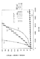
【0104】
ここで、図6は、磁気ブラシ帯電器2の10万枚の耐久に伴う帯電性能△V(飽和電位と1周目で帯電できる電位の差)の変動を示したものである。帯電性能△Vは小さければ小さいほど帯電性が良いことを示しており、1周目で所望の帯電電位に近い値まで帯電できれば、前周の履歴を残すことなく均一な帯電が行えていることになる。
【0105】
図6において(a)はトナーの消費量が1枚あたり0.02gの場合、(b)はトナーの消費量が1枚あたり0.10gの場合であり、画像比率を変えて帯電性能の変動を調べている。
【0106】
図6の(a)と(b)の対比からもわかるように、帯電性能の低下は、枚数依存だけではなく、トナーの消費量が多いほど早く低下している。
【0107】
このことから、帯電性を維持するために磁気ブラシ帯電器2の接触帯電部材としての磁気ブラシ24aの帯電キャリアの抵抗アップ防止を行うには、耐久枚数に応じた対策だけでなく、トナーの消費量に応じた対策が必要であることがわかる。
【0108】
そこで本実施例においては、前記したように、磁気ブラシ帯電器2の帯電器容器21の上側に帯電キャリア収容室27(図1)を設け、この収容室27内に適当量の補給入れ替え用としての帯電キャリア24を収容させた。この帯電キャリア収容室27の底部と帯電器容器21の上側とはシャッタ機構部28を介して連通させ、シャッタ機構部28の開き制御により帯電キャリア収容室27から帯電器容器21内の帯電スリーブ22上に所定量の帯電キャリアが補給されるようにした。また帯電スリーブ22に磁気拘束されて担持されている帯電キャリアの磁気ブラシ24aから適当量の帯電キャリアを剥ぎ取る帯電キャリア剥ぎ取り部材としてのブレード部材26を配設した。
【0109】
そして、プリンターのトナーの使用量に対応して、
▲1▼.シャッタ機構部28を開かせて図3の(b)のように帯電キャリア収容室27から帯電器容器21内の帯電スリーブ22上に所定量の帯電キャリア24の補給を行なわせた。シャッタ機構部28は所定量の帯電キャリア24を帯電器容器21内に補給した後は閉じ状態に再転換させた。
【0110】
具体的にはトナー消費量が100g時毎に帯電キャリアを1g補給するように設定した。
【0111】
▲2▼.またこの帯電キャリア収容室27から帯電器容器21内への帯電キャリアの補給に際してはブレード部材26を図3の(b)のように磁気ブラシ24aに接触した剥ぎ取り位置に転換させて磁気ブラシ24aの帯電キャリアを上記の補給量にほぼ見合う量分剥ぎ取らせた。磁気ブラシ24aから剥ぎ取られた帯電キャリアは本例ではクリーナー7のクリーニング容器71内に落下して収容される。ブレード部材26は磁気ブラシ24aから所定量の帯電キャリアを剥ぎ取った後は帯電スリーブ22の磁気ブラシ層24aから非接触に逃げ離れた退避位置にに再転換させた。
【0112】
上記▲1▼の帯電器容器21内への帯電キャリア24の補給動作と、▲2▼の磁気ブラシ24aからの帯電キャリアの剥ぎ取り動作により、帯電スリーブ22上に形成担持される磁気ブラシ24aの帯電キャリアの一部入れ替えがなされて磁気ブラシ24aがリフレッシュされ、帯電性能の低下が改善される。
【0113】
上記の帯電キャリアの補給入れ替え制御動作▲1▼・▲2▼は、プリンターの繰り返しの画像形成の実行に伴うトナーの消費量が不図示の制御回路で演算検知され、そのトナー消費量情報に基づいて制御回路がシャッタ機構の開閉制御とブレード部材26の揺動制御を行うことで実行される。
【0114】
ここで、トナー消費量の管理は、現像器4の現像容器41へのトナーホッパー48からのトナー補給量を制御回路において記録(メモリ)することにより行うことができる。
【0115】
現像器4の現像容器41へのトナーの補給については、例えば本実施例のように2成分現像の場合には現像剤44のトナーtと現像キャリアcの混合比率を一定にするように、光学検知方法やインダクタンス検知方法により直接混合比率を測定する方法や、画像データからトナー消費量を計算して補給する方法や、感光ドラムや転写ベルト等にパッチを現像し、その濃度を光学検知するなどの方法により少量ずつトナー補給する方法がある。また、1成分現像の場合には前述の画像データからトナー消費量を計算する方法がある。
【0116】
また、磁気ブラシ帯電器2の磁気ブラシ24aの汚染する速度がある程度遅い場合には、必ずしもトナーの補給量を管理しなくても、例えば2成分現像の場合はトナーホッパー48、1成分現像の場合は現像容器内のトナーがなくなり残量検知信号が働いたときに、上記の帯電キャリアの補給入れ替え制御動作▲1▼・▲2▼を行なわせるようにしても良い。
【0117】
本実施例では、2成分現像を採用したため上記の中から現像剤のインダクタンスを検知して、トナーと現像キャリアの混合比率をモニターし一定に保つようにトナーの補給を施し、その際のトナー補給量を記録し管理する方法を採った。
【0118】
上記のようにトナーの消費量に合わせて、磁気ブラシ帯電器2の帯電キャリアを少量ずつ補給入れ替えしていくことによって、接触帯電部材としての磁気ブラシ24aの耐久に伴う汚染の進行に起因する帯電性能の低下が著しく改善された。
【0119】
ここで、図7は図6と同様に磁気ブラシ帯電器2の10万枚の耐久に伴う帯電性能△Vの変動を示したものであり、
(a)はトナーの消費量が1枚あたり0.02gの場合で、帯電キャリアの補給入れ替えを全くしない場合(図6の(a)と同じ)
(b)はトナーの消費量が1枚あたり0.02gの場合で、5000枚ごとに1gの帯電キャリアの補給入れ替えを行った場合
(c)はトナーの消費量が1枚あたり0.10gの場合で、帯電キャリアの補給入れ替えを全くしない場合(図6の(b)と同じ)
(d)はトナーの消費量が1枚あたり0.10gの場合で、5000枚ごとに1gの帯電キャリアの補給入れ替えを行った場合
(e)はトナーの消費量が1枚あたり0.10gの場合で、1000枚ごとに1gの帯電キャリアの補給入れ替えを行った場合である。
【0120】
図7の結果から、(a)・(c)に比べて(b)・(e)は、10万枚時点でもほとんど帯電性能が変動していない。
【0121】
また、(d)は帯電キャリアの補給入れ替えは行っているがトナーの消費量に対して補給入れ替えのタイミングが遅いため、徐々に帯電能が低下してしまっていることかわかる。
【0122】
また、(a)〜(e)は同じ画像チャートで耐久を行ったが、画像比率の違う様々なチャートを用い耐久を行い、トナーの補給量が100gに達した時に帯電カリアを1g補給するようなシーケンスで行った場合においても、(b)や(e)のように常に良好な帯電性を維持することができた。
このように、画像出力枚数ではなく、トナーの消費量に対応して磁気ブラシ帯電器の帯電キャリアの補給入れ替えを行うことにより、接触帯電部材である磁気ブラシの帯電キャリア表面に対するトナー樹脂の融着や外添剤の付着による抵抗値アップを防止し抵抗値を一定に保つことにより磁気ブラシ帯電器の帯電性能を維持することが可能となった。
【0123】
〈実施例2〉(図8・図9)
本実施例は上述の実施例1のプリンターにおいてクリーナー7を除去してクリーナーレスシステムのプリンターにした。図8はこのクリーナーレスシステムのプリンターの概略構成模型図である。クリーナー7が無い以外の装置構成は実施例1のプリンターと同様であるので再度の説明は省略する。
【0124】
本実施例において用いたクリーナーレスシステムについて簡単に説明すると、トナー像転写の際に転写材Pに行かずに感光ドラム1上に残ってしまった転写残トナーは、磁気ブラシ帯電器2の接触帯電部材である磁気ブラシ24aによって回収され、磁気ブラシ24a中の帯電キャリアとの摩擦帯電及び印加バイアスの影響によって−極性に帯電され、感光ドラム1上に吐き出される。吐き出された−極性のトナーは現像器4に現像同時回収され再利用される。
【0125】
この現像同時回収は現像時のかぶりとり電位Vbackを利用している。通常現像工程においては、現像器4に印加する直流電圧と感光ドラム1の表面電位間に電位差を設けることによって、かぶりを防止することを実現している。このかぶり防止のための電位差をかぶり取り電位Vbackと呼ぶが、この電位差によって現像時に感光ドラム面の非画像領域にトナーが付くのを防止するのとともに、クリーナーレス装置においては転写残りトナーの回収も行なっている。
【0126】
このクリーナーレスシステムにおいて感光ドラムの帯電手段は必ずしも磁気ブラシ帯電器に限られるものではないが、例えば導電性ローラを用いた帯電器の場合には比表面積が少ないため表面にトナーが付着するとその部分は帯電不良となってしまい、またコロナ帯電器を用いた場合にはトナーがあっても帯電は行えるが、放電性生物等が付着しやすい点や転写効率が低下した場合など、転写残トナーのパターンで残るため、像露光が遮られたり、現像部での回収不良が発生したりする。
【0127】
これに対して、磁気ブラシ帯電器2を用いた場合には比表面積が大きいため、トナーが多少混入しても帯電性は大きくは低下しない(融着の場合は低下する)ことに加えて、転写残トナーを一度回収し吐き出すため、転写残トナーの残り方が非パターン化されるため転写効率が低下した場合も像露光の遮光や現像での回収不良が発生しにくい。
【0128】
このようなクリーナーレス装置を用いた場合には、磁気ブラシ24aの帯電キャリアの抵抗値の上昇が、クリーナーがある装置に場合に比べて顕著となり、本発明の効果は特に大きい。
【0129】
本実施例においては磁気ブラシ帯電器2についての前述の帯電キャリア補給入れ替え制御▲1▼・▲2▼を、トナー消費量が100g時に帯電キャリアが2g補給されるように設定した。ブレード部材26により磁気ブラシ24aから適量剥ぎ取られた帯電キャリアは帯電器容器21内の底部に落下して収容される。
【0130】
このようにトナーの補給に合わせて、磁気ブラシ帯電器2の帯電キャリアを少量ずつ補給入れ替えしていくことによって、本実施例のようにクリーナーレス装置の場合においても磁気ブラシ帯電器2の耐久に伴う帯電性能の低下が著しく改善された。
【0131】
ここで、図9は磁気ブラシ帯電器2の10万枚の耐久に伴う帯電性能△Vの変動を示したものであり、
(a)はトナーの消費量が1枚あたり0.02gの場合で、帯電キャリアの補給入れ替えを全くしない場合
(b)はトナーの消費量が1枚あたり0.02gの場合で、5000枚ごとに2gの帯電キャリアの補給入れ替えを行った場合
(c)はトナーの消費量が1枚あたり0.10gの場合で、帯電キャリアの補給入れ替えを全くしない場合
(d)はトナーの消費量が1枚あたり0.10gの場合で、5000枚ごとに2gの帯電キャリアの補給入れ替えを行った場合
(e)はトナーの消費量が1枚あたり0.10gの場合で、1000枚ごとに2gの帯電キャリアの補給入れ替えを行った場合である。
【0132】
図9の結果から、(a)・(c)に比べて(b)・(e)は、10万枚時点でもほとんど帯電性能が変動していない。また、(d)は帯電キャリアの補給入れ替えは行っているが、トナーの消費量に対して帯電キャリアの補給入れ替えのタイミングが遅いため、徐々に帯電能が低下してしまっていることかわかる。
【0133】
また、(a)〜(e)は同じ画像チャートで耐久を行ったが、画像比率の違う様々なチャートを用い耐久を行い、トナーの補給量が100gに達した時に帯電キャリアを2g補給するようなシーケンスで行った場合においても、(b)や(e)のように常に良好な帯電性を維持することができた。
【0134】
このように、トナーの消費量に合わせて、帯電キャリアの補給入れ替えを行うことにより、クリーニング手段を具備しないクリーナーレス装置においても、帯電キャリア表面に対するトナー樹脂の融着や外添剤の付着による抵抗値アップを防止し抵抗値を一定に保つことにより磁気ブラシ帯電器の帯電性能を維持することが可能となった。
【0135】
〈実施例3〉(図10・図11)
実施例1や同2においては、感光ドラム1として有機感光体上にその抵抗が109 〜1014Ω・cmの材質を有する表面層を持つものを用いたが、本実施例においては感光ドラム1としてアモルファスシリコン感光体を使用した。
【0136】
その他のプリンター構成は実施例1や同2のプリンターと同様であるので再度の説明を省略する。
【0137】
アモルファスシリコン感光体は上記の有機感光体と同様に注入帯電が可能な感光体であるが、誘電率が有機感光体が3〜4程度であるのに対して、アモルファスシリコン感光体は11〜12程度と大きいため、帯電時に必要なドラム電流量が大きくなる。
【0138】
このため、耐久初期は有機感光体とほぼ同等の帯電性能が得られているが、接触帯電部材としての磁気ブラシ24aの帯電キャリアの抵抗がアップすると帯電性能が急激に低下する。
【0139】
そこで、感光ドラム1としてアモルファスシリコン感光体を用いたプリンターについて、それが実施例1のようにクリーナー7を有するプリンターの場合には磁気ブラシ帯電器2についての前述の帯電キャリア補給入れ替え制御▲1▼・▲2▼を、トナー消費量が100g時に帯電キャリアが1.5g補給されるように設定し、また実施例2のようにクリーナーレスのプリンターの場合にはトナー消費量が100g時に帯電キャリアが3g補給されるように設定した。
【0140】
このようにトナーの補給に合わせて、磁気ブラシ帯電器2の帯電キャリアを少量ずつ補給・入れ替えしていくことによって、感光ドラム1としてアモルファスシリコン感光体を用いた場合においても磁気ブラシ帯電器2の耐久に伴う帯電性能の低下が著しく改善された。
【0141】
ここで、図10は、感光ドラム1としてアモルファスシリコン感光体を用い、クリーナー7を具備したプリンターについて、磁気ブラシ帯電器2の10万枚の耐久に伴う帯電性能△Vの変動を示したものであり、
(a)はトナーの消費量が1枚あたり0.02gの場合で、帯電キャリアの補給入れ替えを全くしない場合、
(b)はトナーの消費量が1枚あたり0.02gの場合で、5000枚ごとに1.5gの帯電キャリアの補給入れ替えを行った場合
(c)はトナーの消費量が1枚あたり0.10gの場合で、帯電キャリアの補給入れ替えを全くしない場合
(d)はトナーの消費量が1枚あたり0.10gの場合で、5000枚ごとに1.5gの帯電キャリアの補給入れ替えを行った場合
(e)はトナーの消費量が1枚あたり0.10gの場合で、1000枚ごとに1.5gの帯電キャリアの補給入れ替えを行った場合である。
【0142】
また、図11は、感光ドラム1としてアモルファスシリコン感光体を用い、クリーナーレスのプリンターについて、磁気ブラシ帯電器2の10万枚の耐久に伴う帯電性能△Vの変動を示したものであり、
(a)はトナーの消費量が1枚あたり0.02gの場合で、帯電キャリアの補給入れ替えを全くしない場合
(b)はトナーの消費量が1枚あたり0.02gの場合で、5000枚ごとに3gの帯電キャリアの補給入れ替えを行った場合
(c)はトナーの消費量が1枚あたり0.10gの場合で、帯電キャリアの補給入れ替えを全くしない場合
(d)はトナーの消費量が1枚あたり0.10gの場合で、5000枚ごとに3gの帯電キャリアの補給入れ替えを行った場合、
(e)はトナーの消費量が1枚あたり0.10gの場合で、1000枚ごとに3gの帯電キャリアの補給入れ替えを行った場合である。
【0143】
図10および図11の結果からどちらの場合も、(a)・(c)に比べて(b)・(e)は、10万枚時点でもほとんど帯電性能が変動していない。
【0144】
また、(d)は帯電キャリアの補給入れ替えは行っているが、トナーの消費量に対して帯電キャリアの補給入れ替えのタイミングが遅いため、徐々に帯電能が低下してしまっていることかわかる。
【0145】
また、(a)〜(e)は同じ画像チャートで耐久を行ったが、画像比率の違う様々なチャートを用い耐久を行い、トナーの補給量が100gに達した時に帯電キャリアを、クリーナー7があるプリンターの場合には1.5g、クリーナーレスプリンターの場合には3g補給するようなシーケンスで行った場合においても、(b)や(e)のように常に良好な帯電性を維持することができた。
【0146】
このように、トナーの消費量に対応して帯電キャリアの補給入れ替えを行うことにより、アモルファスシリコンを感光体として用いた場合においても、帯電キャリア表面に対するトナー樹脂の融着や外添剤の付着による抵抗値アップを防止し抵抗値を一定に保つことにより磁気ブラシ帯電器2の帯電性能を維持することが可能となった。
【0147】
〈実施例4〉(図12)
実施例1・同2・同3の各プリンターにおいては、帯電バイアスとして−650Vの直流バイアスを磁気ブラシ帯電器2の帯電スリーブ22に印加することにより感光ドラム1の帯電を行ったが、本実施例においては帯電バイアスとして、上記直流バイアスに対して、さらに1000HZ、700Vの交番電圧を重畳したDC+ACバイアスを磁気ブラシ帯電器2の帯電スリーブ22に印加することにより感光ドラム1の帯電を行った。
【0148】
帯電バイアスに交番電圧を重畳することにより帯電性が向上することに加えて、例えば実施例2のようにクリーナーレス装置の場合には、転写残りトナーの磁気ブラシへの回収及び吐き出しの効率が向上する。
【0149】
図12は、実施例2と同様のプリンター構成で、磁気ブラシ帯電器2の帯電スリーブ22に印加する帯電バイアスを上記の交番電圧を重畳したDC+ACバイアスとした場合の、磁気ブラシ帯電器2の10万枚の耐久に伴う帯電性能△Vの変動を示したものであり、本実施例においても前述の帯電キャリア補給入れ替え制御▲1▼・▲2▼を行った。
【0150】
具体的には交番電圧を印加することにより帯電性能が向上したため、トナー消費量が100g時に帯電キャリアを1g補給するように設定した。
【0151】
(a)はトナーの消費量が1枚あたり0.02gの場合で、帯電キャリアの補給入れ替えを全くしない場合
(b)はトナーの消費量が1枚あたり0.02gの場合で、5000枚ごとに1gの帯電キャリアの補給入れ替えを行った場合
(c)はトナーの消費量が1枚あたり0.10gの場合で、帯電キャリアの補給入れ替えを全くしない場合
(d)はトナーの消費量が1枚あたり0.10gの場合で、5000枚ごとに1gの帯電キャリアの補給入れ替えを行った場合
(e)はトナーの消費量が1枚あたり0.10gの場合で、1000枚ごとに1gの帯電キャリアの補給入れ替えを行った場合である。
【0152】
図12の結果から、(a)・(c)に比べて(b)・(e)は10万枚時点でもほとんど帯電性能が変動していない。
【0153】
また、(d)は帯電キャリアの補給入れ替えは行っているが、トナーの消費量に対して帯電キャリアの補給入れ替えのタイミングが遅いため、徐々に帯電能が低下してしまっていることかわかる。
【0154】
また、(a)〜(e)は同じ画像チャートで耐久を行ったが、画像比率の違う様々なチャートを用い耐久を行い、トナーの補給量が100gに達した時に帯電キャリアを1g補給するようなシーケンスで行った場合においても、(b)や(e)のように常に良好な帯電性を維持することができた。
【0155】
このように、帯電バイアスに交番電圧を重畳した場合、帯電性能が向上するため直流バイアスのみを印加した場合よりも、帯電キャリアの補給入れ替え量を減らすことができる。
【0156】
〈実施例5〉(図13・図14)
実施例1〜同4においては、現像器4として2成分現像器を用い、現像材44の現像キャリアcとトナーtの混合比率をインダクタンス検知法によって一定に保つようにトナーを補給する際の補給量を管理して、トナーの消費量に応じて帯電キャリアを補給入れ替えしたが、本実施例においては、2成分現像器4にトナーを補給するためのトナーホッパー(トナー容器)48内の500gのトナーがほぼ無くなりトナー残量検知手段(不図示)が働いた時点で帯電キャリアを補給入れ替えするタイミングをとった。
【0157】
即ちトナーホッパー48内のトナーがほぼ無くなったことが残量検知手段で検知されると、その検知信号が制御回路(不図示)に入力する。制御回路はその入力信号に基づいて前述の帯電キャリア補給入れ替え制御▲1▼・▲2▼を実行する。また警告・表示手段(不図示)を作動させてオペレーターにトナーホッパー48へのトナー補給を促す。
【0158】
このような方法を採るためには、磁気ブラシ24aの帯電キャリア汚染の進行速度が遅い条件や基本的な帯電特性が高い場合が好ましいが、実施例1〜同4のようにトナーの消費量をデータとして管理する必要がないためコストの低減がはかれる。
【0159】
本実施例においては、実施例1のように磁気ブラシ24aの帯電キャリア汚染の進行速度が遅い条件であるクリーニング手段7を具備する装置で、帯電バイアスとして−650Vの直流バイアスを帯電スリーブ22に印加した場合と、実施例4のようにクリーナーレス装置のように基本的な帯電特性が高い条件の装置で、帯電バイアスとして−650Vの直流バイアスに対して、1000HZ・700Vの交番電圧を重畳したDC+ACバイアスを帯電スリーブ22に印加した場合の装置についてそれぞれ耐久を行った。
【0160】
ここで、図13は、クリーナー7を具備したプリンターで、かつ直流バイアスの帯電条件で、10万枚の耐久に伴う帯電性能△Vの変動を示したものであり、(a)はトナーの消費量が1枚あたり0.02gの場合で、帯電キャリアの補給入れ替えを全くしない場合
(b)はトナーの消費量が1枚あたり0.02gの場合で、ホッパー48内の500gのトナーが無くなる25000枚ごとに5gの帯電キャリアの補給入れ替えを行った場合
(c)はトナーの消費量が1枚あたり0.10gの場合で、帯電キャリアの補給入れ替えを全くしない場合
(d)はトナーの消費量が1枚あたり0.10gの場合で、ホッパー48内の500gのトナーが無くなる5000枚ごとに5gの帯電キャリアの補給入れ替えを行った場合である。
【0161】
また、図14は、クリーナーレスのプリンターで、かつ直流バイアスに交番電圧を重畳した帯電条件で、10万枚の耐久に伴う帯電性能△Vの変動を示したものであり、
(a)はトナーの消費量が1枚あたり0.02gの場合で、帯電キャリアの補給入れ替えを全くしない場合
(b)はトナーの消費量が1枚あたり0.02gの場合で、トナーホッパー48内の500gのトナーが無くなる25000枚ごとに5gの帯電キャリアの補給入れ替えを行った場合
(c)はトナーの消費量が1枚あたり0.10gの場合で、帯電キャリアの補給入れ替えを全くしない場合
(d)はトナーの消費量が1枚あたり0.10gの場合で、トナーホッパー48内の500gのトナーが無くなる5000枚ごとに5gの帯電キャリアの補給入れ替えを行った場合である。
【0162】
図13および図14の結果からどちらの場合も、(a)・(c)に比べて(b)・(d)は10万枚時点でもほとんど帯電性能が変動していないことかわかる。
【0163】
また、(a)〜(d)は同じ画像チャートで耐久を行ったが、画像比率の違う様々なチャートを用い耐久を行い、トナーホッパー48内の500gのトナーが無くなった時に帯電キャリアを5g補給するようなシーケンスで行った場合においても、(b)や(d)のように常に良好な帯電性を維持することができた。
【0164】
〈その他〉
1)帯電キャリア補給入れ替え制御は画像形成時に実行させてもよいし、非画像形成時に実行させてもよい。
【0165】
2)各実施例においては、現像器4を、トナー粒子tと帯電キャリアcを混合した2成分現像剤を用いた2成分現像器としたが、現像器4は2成分現像器に限られるものではなく、1成分現像器等すべての現像方法において可能である。
【0166】
反転現像方式でも、正規現像方式でもよい。好ましくは、現像剤が感光体に対して接触状態で現像する、1成分接触現像や2成分接触現像がより現像時の同時回収効果を高めるのに効果がある。
【0167】
また、現像剤中のトナー粒子としては粉砕トナー等においても可能であるし、更に好ましくは、重合トナーを用いた場合には、1成分接触現像や2成分接触現像はもちろん1成分非接触現像や2成分非接触現像などの他の現像方法においても転写残りトナーの充分な回収効果が得られる。
【0168】
3)トナーの消費量の検知方法も、2成分現像の場合には、インダクタンス検知や光学検知等により直接現像剤中のトナー濃度を測定する方法や、感光ドラムや転写シート上にパッチを現像し濃度測定をすることによってトナー濃度を割り出す方法であるバッチ検出法等によってトナーを補給していく際にトナー消費量を記録したり、画像信号からトナーの消費量を割り出す方法など様々な方法があり、1成分現像の場合には画像信号から割り出す方法や現像容器内のトナー量の推移を光学検知等で管理する方法などがあるが、いずれの場合でもトナーの消費量に合わせて、帯電キャリアを補給していくことによって効果が見られた。
【0169】
4)また、磁気ブラシの帯電キャリア汚染の進行が遅い場合や帯電の基本性能が高い場合などは、実施例5のように、1成分現像の場合でもトナーホッパーや現像容器内のトナーがほぼ無くなったタイミングで帯電キャリアの補給を行っても良い。
【0170】
5)トナーの消費量に対する帯電キャリアの補給量や、補給のタイミング等についても、各実施例の量及び枚数はごく一例であり、トナーの消費量に対応して帯電用帯電キャリアを補給することによりすべての場合で効果が得られた。
【0171】
6)また、感光体についても、表面抵抗が109 〜1014Ω・cmの低抵抗層を持つことが電荷注入を実現できオゾンの発生防止の面から望ましいが、上記以外の有機感光体等でも、耐久性向土のためには充分な効果が得られる。
【0172】
7)磁気ブラシからの帯電キャリアの剥ぎ取り手段は実施例のブレード部材26に限られず任意の手段構成にすることができる。
【0173】
更に、各実施例においては帯電キャリアの補給に伴い、使用した帯電キャリアを磁気ブラシから適量剥ぎ取ったが、全てを剥ぎ取って全て新しい帯電キャリアに入れ替えても良い。また例えば感光体への付着等で帯電キャリアの減少が顕著な場合には、必ずしも剥ぎ取りを行う必要はない。
【0174】
8)また、帯電器2の構成についても各実施例では、内部に固定マグネットを配し、回転可能な非磁性スリーブの回転によって帯電キャリアを搬送したが、このような構成に限られるものではなく、マグネット自体が回転する構成など、帯電キャリアを用いた接触帯電において、トナーの消費量に対応して帯電キャリアの供給を行う帯電器のすべてを含んでいる。
【0175】
9)接触帯電部材に対する帯電バイアス印加をACバイアス印加方式で行なう場合の交流バイアス成分の波形としては、正弦波、矩形波、三角波等適宜使用可能である。また、交流バイアスは、例えば直流電源を周期的にON・OFFすることによって形成された矩形波の電圧を含む。この時交流バイアスを制御するとは、そのピーク間電圧を制御すればよい。このように、交流バイアスは、周期的にその電圧値が変化するようなバイアスが使用できる。
【0176】
現像器に印加する現像バイアスに交流バイアス成分を含ませる場合のその交流バイアスについても上記と同様である。
【0177】
10)像担持体の帯電面に対する情報書き込み手段としての画像露光手段は、実施形態例のようなLED露光手段に限定されるものではなく、通常のアナログ的な画像露光手段や、レーザー走査露光手段、蛍光灯等の発光素子と液晶シャッタ等の組み合わせによるものなど、画像情報に対応した静電潜像を形成できるものであればよい。
【0178】
像担持体は静電記録誘電体などであってもよい。この場合は、該誘電体面を所定の極性・電位に一様に一次帯電した後、除電針ヘッド、電子銃等の除電手段で選択的に除電して目的の静電潜像を書き込み形成する。
【0179】
11)転写方法としてはローラ転写、ブレード転写、コロナ放電転写などであってもよい。転写ドラムや転写ベルトなどの中間転写体を用いて、単色画像形成ばかりでなく多重転写等により多色、フルカラー画像を形成する画像形成装置にも適用可能である。
【0180】
12)像担持体、帯電器、現像器等の任意のプロセス機器を画像形成装置本体に対して一括して着脱交換自在のプロセスカートリッジ着脱式の装置構成のものにすることもできる。
【0181】
13)像担持体としての電子写真感光体や静電記録誘電体を回動ベルト型にし、これに帯電・潜像形成・現像の工程手段により所要の画像情報に対応したトナー像を形成させ、そのトナー像形成部を閲読表示部に位置させて画像表示させ、像担持体は繰り返して表示画像の形成に使用する画像表示装置(ディスプレイ装置)もある。本発明の画像形成装置にはそのような画像表示装置も含む。
【0182】
【発明の効果】
以上説明したように、磁気ブラシ接触帯電方式・転写方式の画像形成装置において接触帯電部材である磁気ブラシの帯電性能の低下は、トナーの消費に伴う帯電用磁性粒子(帯電キャリア)へのトナー融着や外添剤付着が主要因であるため、本発明のようにトナーの消費量に対応して磁性粒子を補給することにより、磁性粒子の汚染による帯電性能の低下を長期にわたって防ぎ、常に良好な画像を維持することが可能となった。
【図面の簡単な説明】
【図1】 実施例1の画像形成装置の概略構成模型図
【図2】 感光ドラムの層構成模型図
【図3】 帯電器の構成模型図
【図4】 現像器の構成模型図
【図5】 トナーの帯電量測定に用いた測定器具の説明図
【図6】 磁気ブラシの帯電キャリアの耐久に伴う汚染による帯電性能の変動を表すグラフ
【図7】 実施例1における各種条件での耐久に伴う帯電性能の変動を表すグラフ
【図8】 実施例2の画像形成装置(クリーナーレス)の概略構成模型図
【図9】 実施例2における各種条件での耐久に伴う帯電性能の変動を表すグラフ
【図10】 実施例3における各種条件での耐久に伴う帯電性能の変動を表すグラフ(その1)
【図11】 実施例3における各種条件での耐久に伴う帯電性能の変動を表すグラフ(その2)
【図12】 実施例4における各種条件での耐久に伴う帯電性能の変動を表すグラフ
【図13】 実施例5における各種条件での耐久に伴う帯電性能の変動を表すグラフ(その1)
【図14】 実施例5における各種条件での耐久に伴う帯電性能の変動を表すグラフ(その2)
【図15】 画像形成装置の一例の概略構成模型図
【符号の説明】
A・・プリンター部、B・・イメージスキャナー部、1・・感光ドラム(像担持体)、2・・磁気ブラシ帯電器、3・・LED露光手段、4・・現像器、5・・給紙カセット、6・・転写ベルト装置、7・・クリーナー、8・・定着器[0001]
BACKGROUND OF THE INVENTION
The present invention uniformly charges an image carrier such as an electrophotographic photosensitive member or an electrostatic recording dielectric, such as a transfer type electrophotographic apparatus or electrostatic recording apparatus, to a predetermined polarity and potential. An image forming apparatus for forming an electrostatic latent image on a charging surface of a carrier, developing the electrostatic latent image as a toner image, transferring the toner image to a transfer material, and repeatedly using the image carrier for image formation About.
[0002]
More specifically, the present invention relates to an image forming apparatus using a magnetic brush charger (magnetic brush charging device) for charging an image carrier with a contact charging member using magnetic particles as a charging means for charging the image carrier.
[0003]
[Prior art]
FIG. 15 is a schematic configuration diagram of an example of a transfer type electrophotographic apparatus (copier, printer, facsimile, etc.) as a conventional example of an image forming apparatus.
[0004]
[0005]
The
[0006]
The electrostatic latent image is developed as a toner image by the developing
[0007]
On the other hand, a transfer material (transfer paper) P as a second image carrier from a paper feed mechanism unit (not shown) is fed to the transfer unit between the
[0008]
Next, the transfer material P is separated from the surface of the rotating
[0009]
The surface of the
[0010]
1) Contact charger
In the image forming apparatus as described above, the
[0011]
For example, a corona charger has been generally used as the charging means 112 for uniformly charging the surface of the
[0012]
In recent years, contact chargers have been put into practical use because they have advantages such as low ozone and low power over corona chargers.
[0013]
The contact charger is a conductive member whose resistance value has been adjusted and is placed in contact with the object to be charged as a contact charging member, and a predetermined voltage (charging bias) is applied to the contact charging member, whereby the surface of the object to be charged Is charged to a predetermined polarity and potential.
[0014]
As the contact charging member, a roller type with a conductive rubber roll (charge roller, conductive rubber roller), a blade type with a conductive rubber blade (charge blade), a magnetic brush type using magnetic particles, a conductive type Various forms such as a fur brush type in which the fibers are formed in a brush shape are preferably used.
[0015]
A magnetic brush charger is one in which conductive magnetic particles are magnetically constrained and held as a magnetic brush directly on a magnet or on a sleeve containing the magnet, and the magnetic brush portion of the magnetic particles is stopped or The surface of the object to be charged is brought into contact with the surface of the object to be charged while being rotated, and a voltage is applied to the surface of the object to be charged, so that the surface of the object is charged.
[0016]
There are a DC bias application method in which the charging bias applied to the contact charging member is only a DC voltage, and an AC bias application method in which an oscillation voltage having a DC bias component and an alternating bias component is used.
[0017]
2) Injection charging
Contact charging includes a system in which charging by a discharge phenomenon is dominant as disclosed in Japanese Patent Publication No. 3-52058 and the like, and a direct charge of a surface to be charged as disclosed in Japanese Patent Laid-Open No. 6-3921 and the like. There is a system (charge injection charging system) in which charging by injection (charging) is dominant.
[0018]
The charge injection charging method uses a contact charging member as described above, and has a surface layer in which conductive fine particles are dispersed on a normal organic photoconductor in the case of an image bearing member, which is charge-chargeable as an object to be charged. By using a photoconductor, an amorphous silicon photoconductor, or the like, it is possible to obtain a charged potential on the surface of the member to be charged that is substantially equal to the direct current component of the bias applied to the contact charging member.
[0019]
This charge injection charging method does not use a discharge phenomenon in which charging to the body of the object is performed using a corona charger, so the applied charging bias required for charging is equal to the desired surface potential of the body to be charged. Therefore, it has been attracting attention because it is possible to achieve complete ozone-less and low-power consumption charging without generation of ozone.
[0020]
[Problems to be solved by the invention]
In an image forming apparatus of a magnetic brush contact charging system / transfer system, if image formation is repeated, the magnetic particles of the magnetic brush as a contact charging member are contaminated and the chargeability is lowered.
[0021]
The cause of contamination of the magnetic particles of the magnetic brush is that the toner particles usually have a relatively high electric resistance, so that the resin component of the toner particles is fused to the magnetic particles or externally added to the toner particles. It is generated by the adhesion of the added external additive. Due to this phenomenon, the resistance of the magnetic particles is increased, and the image carrier, which is a charged body, cannot be charged to a desired potential or charging unevenness occurs, resulting in an image defect.
[0022]
In view of this, the present invention is intended to prevent deterioration of charging performance due to contamination of magnetic particles of a magnetic brush as a contact charging member over a long period of time, particularly for a magnetic brush contact charging type / transfer type image forming apparatus, and always maintain a good image. Objective.
[0023]
[Means for Solving the Problems]
The present invention is an image forming apparatus having the following configuration.
[0024]
(1) The image carrier is charged by a contact charging member using magnetic particles, an electrostatic latent image is formed on the charging surface of the image carrier, the electrostatic latent image is developed as a toner image, and the toner In an image forming apparatus in which an image is transferred to a transfer material and an image carrier is repeatedly used for image formation, magnetic particles are replenished in accordance with the amount of toner consumed.
[0025]
(2) The image forming apparatus according to (1), wherein the replenishment of the magnetic particles corresponding to the toner consumption amount is based on a signal from a detection unit that detects the toner consumption amount.
[0026]
(3) The image forming apparatus according to (1), wherein the magnetic particle replenishment corresponding to the toner consumption is performed at a toner replenishment timing by a toner remaining amount detecting means in the toner container.
[0027]
(4) The image forming apparatus according to any one of (1) to (3), wherein at the time of supplying magnetic particles, at least a part of the used magnetic particles of the contact charging member is peeled off.
[0028]
(5) The developing means for developing the electrostatic latent image formed on the image carrier as a toner image also serves as a cleaning means for collecting residual toner particles remaining on the image carrier after the toner image is transferred to the transfer material. The image forming apparatus according to any one of (1) to (4).
[0029]
(6) The image forming apparatus according to any one of (1) to (5), wherein the bias applied to the contact charging member is an alternating voltage superimposed on a DC bias.
[0030]
(7) The image carrier is 10 on the surface.9 -1014The image forming apparatus according to any one of (1) to (6), further including a layer made of a material of Ω · cm.
[0031]
(8) The image carrier is 10 on the surface of the organic photoreceptor.9 -1014The image forming apparatus according to any one of (1) to (6), wherein the image forming apparatus has a surface layer made of a material of Ω · cm.
[0032]
(9) The image forming apparatus according to any one of (1) to (6), wherein the image carrier is made of an amorphous silicon material.
[0033]
<Operation>
That is, in the magnetic brush contact charging type / transfer type image forming apparatus, it was examined what the degree of contamination of the magnetic particles of the magnetic brush as the contact charging member depends on. It has been found that the amount of consumption (use) is large. For example, it has been found that even with the same output of 10,000 sheets, the contamination state is greatly different when the image ratio is high and low, and when the image ratio is high, the degree of contamination is severe.
[0034]
Therefore, in the present invention, the magnetic brush is refreshed by supplying new magnetic particles to the magnetic brush, which is a contact charging member, corresponding to the amount of toner consumed in the image forming process, and charging due to contamination of the magnetic particles of the magnetic brush is performed. It was possible to prevent deterioration in performance over a long period of time and maintain a good image at all times.
[0035]
DETAILED DESCRIPTION OF THE INVENTION
<Example 1> (FIGS. 1 to 7)
FIG. 1 is a schematic configuration diagram of an example of an image forming apparatus according to the present invention.
[0036]
The image forming apparatus of this example is a printer using a transfer type electrophotographic process, a magnetic brush contact charging method, an LED exposure method, and a reverse development method.
[0037]
In FIG. 1, A is a printer unit, and B is an image reader unit (image reading device) mounted on the printer unit.
[0038]
(1) Image reader part B
In the image reader unit B,
[0039]
An
[0040]
In the forward drive process of the
[0041]
The
[0042]
In other words, the image information of the original G is photoelectrically read as a time-series electric digital pixel signal (image signal) by the image reader unit B.
[0043]
(2) Printer part A
[0044]
a. Charging: The
[0045]
b. Exposure: The uniform exposure surface of the rotating
[0046]
That is, the
[0047]
c. Current image: The electrostatic latent image formed on the surface of the rotating
[0048]
d. Transfer: On the other hand, the transfer material P as the second image bearing member loaded and stored in the
[0049]
The
[0050]
The transfer material P is transported to the transfer unit T on the upper surface of the ascending belt portion of the belt 6a. When the leading end of the transport transfer material P enters the transfer portion T, a predetermined transfer bias is supplied from a transfer bias application power source (not shown) to the
[0051]
e. Fixing: The transfer belt 6a also serves as a transfer means for transferring the transfer material P from the transfer portion T to the heat roller
[0052]
f. Cleaning: Further, the surface of the rotating
[0053]
The
[0054]
(3)
As the
[0055]
The
[0056]
First layer 1b; an undercoat layer, which is a conductive layer having a thickness of 20 μm provided for leveling defects of the drum base 1a.
[0057]
Second layer 1c is a positive charge injection preventing layer, and serves to prevent the positive charge injected from the drum base 1a from canceling the negative charge charged on the surface of the photoreceptor, and is formed by amylan resin and methoxymethylated nylon. 1 × 10⁶ This is a medium resistance layer having a thickness of 1 μm, the resistance of which is adjusted to about Ω · cm.
[0058]
Third layer 1d: a charge generation layer, which generates positive and negative charge pairs upon exposure to a layer having a thickness of about 0.3 μm in which a disazo pigment is dispersed in a resin.
[0059]
Fourth layer 1e: a charge transport layer, which is a P-type semiconductor in which hydrazone is dispersed in a polycarbonate resin. Therefore, the negative charge charged on the surface of the photoreceptor cannot move through this layer, and only the positive charge generated in the charge generation layer can be transported to the surface of the photoreceptor.
[0060]
Fifth layer 1f; charge injection layer, SnO as conductive fine particles in binder of insulating resin2 It is a coating layer of a material in which 1 g of ultrafine particles are dispersed. Specifically, SnO having a particle size of 0.03 μm is obtained by reducing the resistance (conducting) by doping an insulating resin with antimony which is a light-transmissive conductive filler.2 It is a coating layer of a material in which particles are dispersed by 70 weight percent with respect to the resin. The coating solution thus prepared was applied to a thickness of about 3 μm by an appropriate coating method such as a dipping coating method, a spray coating method, a roll coating method, or a beam coating method to form a charge injection layer.
[0061]
(4)
FIG. 3 is a partially enlarged model view of the
[0062]
[0063]
[0064]
[0065]
[0066]
[0067]
A charge
[0068]
The present example is a blade member that can swing around a
[0069]
[0070]
A
[0071]
The charging
[0072]
Then, a predetermined charging bias is applied from a charging bias application power source (not shown) to the magnetic brush 24a via the charging
[0073]
As the charging
Average particle size: 10-100 μm
Saturation magnetization: 20 to 250 emu / cmThree,
Resistance: 1 × 10² ~ 1x10TenΩ · cm
Can be used. Considering the existence of insulation defects such as pinholes in the
[0074]
In order to improve the charging performance, it is better to use the one with the smallest possible resistance.
Average particle size: 25 μm
Saturation magnetization: 200emu / cmThree
Resistance: 5 × 10⁶ Ω · cm
The magnetic particles were used. Further, the
[0075]
Here, the resistance value of the magnetic particles for charging has a bottom area of 228 mm.2 After putting 2g of carrier into the metal cell, 6.6Kg / cm2 And applying a voltage of 100V for measurement.
[0076]
(5)
Generally, electrostatic latent image development methods are roughly classified into the following four types.
[0077]
a. For non-magnetic toner, the sleeve is coated on the sleeve with a blade or the like, and the magnetic toner is coated by magnetic force and conveyed to develop in a non-contact state with respect to the photosensitive drum (one-component non-contact development).
[0078]
b. A method in which the toner coated as described above is developed in contact with the photosensitive drum (one-component contact development).
[0079]
c. A method in which toner particles are mixed with a magnetic carrier as a developer and conveyed by magnetic force and developed in contact with a photosensitive drum (two-component contact development).
[0080]
d. A method in which the above two-component developer is developed in a non-contact state (two-component non-contact development).
[0081]
The two-component contact development method c is often used from the viewpoint of high image quality and high stability.
[0082]
The developing
[0083]
The developing
[0084]
In the two-
[0085]
A mixture of the toner t and the developing carrier c at a weight ratio of 8:92 was used as the
[0086]
The toner t in the
[0087]
First, a two-component agent in which toner particles t to be measured for triboelectric charge and development carrier c are mixed at a weight ratio of 5:95 is put into a polyethylene bottle having a capacity of 50 to 100 ml, and manually for about 10 to 40 seconds. Shake and take about 0.5 to 1.5 g of the two-component agent, put it in a
[0088]
The total weight of the
[0089]
Next, in the suction device 101 (at least the insulator is in contact with the measurement container 102), suction is performed from the
[0090]
In this state, the resin is removed by suction for 2 minutes. The potential of the electrometer 109 at this time is set to V (volt). Here, 108 is a capacitor, and the capacity is C (F). Further, the weight of the
[0091]
The triboelectric charge amount of the toner is calculated as the following formula.
[0092]
Resin triboelectric charge (c / kg) = C × V × 10-3/ (W1-W2)
Next, a developing process for developing an electrostatic latent image on the
[0093]
In FIG. 4, the developing
[0094]
The developer thin layer 44a on the developing
[0095]
A DC voltage and an AC voltage are applied to the developing
DC voltage: -480V
AC voltage; Vpp = 1500V, Vf = 3000Hz
Is applied.
[0096]
In general, in the two-component development method, when an AC voltage is applied, the development efficiency increases and the image becomes high-quality, but conversely, there is a risk that fogging easily occurs. For this reason, in general, it is possible to prevent fogging by providing a potential difference between the DC voltage applied to the developing
[0097]
This potential difference for preventing fogging is called fogging potential (Vback). This potential difference prevents toner from adhering to a non-image area (non-exposed portion) on the surface of the
[0098]
The toner density is monitored by a sensor (not shown) that detects the toner density of the
[0099]
In this embodiment, since the two-component development is adopted, the inductance of the
[0100]
(6) Charge carrier replenishment replacement control
As in the printer of the above example, even if the image forming apparatus includes a
[0101]
For this reason, the slipped particles and toner particles are carried to the charging unit N as the
[0102]
The toner mixed in the magnetic brush 24a is aligned with a normal charging polarity (negative polarity in this embodiment) by frictional charging with the charging carrier of the magnetic brush 24a, and is discharged again from the magnetic brush 24a onto the photosensitive drum 1 ( (Because the charged potential is slightly lower than the applied bias). The toner discharged from the magnetic brush 24a onto the
[0103]
When image output is performed in the above-described process, the toner that has passed through the
[0104]
Here, FIG. 6 shows the fluctuation of charging performance ΔV (the difference between the saturation potential and the potential that can be charged in the first round) with the endurance of 100,000 sheets of the
[0105]
6A shows the case where the toner consumption amount is 0.02 g per sheet, and FIG. 6B shows the case where the toner consumption amount is 0.10 g per sheet. I'm investigating.
[0106]
As can be seen from the comparison between (a) and (b) of FIG. 6, the decrease in charging performance is not only dependent on the number of sheets but also decreases more rapidly as the amount of toner consumption increases.
[0107]
Therefore, in order to prevent the charge carrier resistance of the magnetic brush 24a as the contact charging member of the
[0108]
Therefore, in the present embodiment, as described above, the charging carrier storage chamber 27 (FIG. 1) is provided above the
[0109]
And corresponding to the amount of toner used in the printer,
(1). The
[0110]
Specifically, 1 g of charge carrier was set to be replenished every 100 g of toner consumption.
[0111]
(2). When supplying the charge carrier from the charge
[0112]
The magnetic carrier 24a formed and supported on the charging
[0113]
In the above charge carrier replenishment control operation (1) and (2), the consumption amount of toner accompanying the execution of repeated image formation by the printer is calculated and detected by a control circuit (not shown), and the toner consumption amount information is used. The control circuit executes the shutter mechanism opening / closing control and the
[0114]
Here, the toner consumption amount can be managed by recording (memory) the toner replenishment amount from the
[0115]
As for the replenishment of toner to the developing
[0116]
Further, when the contamination speed of the magnetic brush 24a of the
[0117]
In this embodiment, since the two-component development is adopted, the toner inductance is detected from the above, and the toner is supplied so that the mixing ratio of the toner and the development carrier is monitored and kept constant. The method of recording and managing the quantity was adopted.
[0118]
As described above, charging due to the progress of contamination accompanying the durability of the magnetic brush 24a as the contact charging member is obtained by replenishing and replacing the charging carrier of the
[0119]
Here, FIG. 7 shows the variation of the charging performance ΔV accompanying the durability of 100,000 sheets of the
(A) is a case where the toner consumption is 0.02 g per sheet, and the charging carrier is not replenished or replaced at all (the same as (a) of FIG. 6).
(B) is a case where the toner consumption is 0.02 g per sheet, and 1 g of charge carrier is replenished and replaced every 5000 sheets.
(C) is the case where the toner consumption is 0.10 g per sheet, and the charging carrier is not replenished or replaced at all (the same as (b) of FIG. 6).
(D) shows the case where the toner consumption is 0.10 g per sheet, and 1 g of charge carrier is replenished and replaced every 5000 sheets.
(E) is a case where the toner consumption is 0.10 g per sheet, and 1 g of charge carrier is replenished and replaced every 1000 sheets.
[0120]
From the results of FIG. 7, the charging performance of (b) and (e) is almost unchanged even at 100,000 sheets as compared to (a) and (c).
[0121]
Further, (d) shows that the charging ability is gradually lowered because the charging carrier is replenished and replaced, but the timing of replenishing and replacing is late with respect to the toner consumption.
[0122]
Further, although (a) to (e) were endured with the same image chart, endurance was performed using various charts with different image ratios so that 1 g of charged carrier was replenished when the toner replenishment amount reached 100 g. Even in the case of a simple sequence, good chargeability could always be maintained as in (b) and (e)..
In this way, the toner carrier is fused to the surface of the charging carrier of the magnetic brush, which is a contact charging member, by replenishing and replacing the charging carrier of the magnetic brush charger according to the amount of toner consumed instead of the number of image outputs. In addition, it is possible to maintain the charging performance of the magnetic brush charger by preventing the resistance value from increasing due to adhesion of external additives and keeping the resistance value constant.
[0123]
<Example 2> (FIGS. 8 and 9)
In this example, the
[0124]
The cleaner-less system used in this embodiment will be briefly described. The transfer residual toner remaining on the
[0125]
This simultaneous development recovery utilizes the fog removal potential Vback during development. In the normal development process, it is possible to prevent fogging by providing a potential difference between the DC voltage applied to the developing
[0126]
In this cleanerless system, the charging means of the photosensitive drum is not necessarily limited to the magnetic brush charger.rollerIn the case of the charger using the toner, since the specific surface area is small, if the toner adheres to the surface, the portion becomes poorly charged, and if the corona charger is used, the toner can be charged even if the toner is present. Since it remains in the pattern of residual toner, such as when dischargeable organisms are likely to adhere or when transfer efficiency is reduced, image exposure is interrupted, and recovery failure occurs at the developing unit.
[0127]
On the other hand, when the
[0128]
When such a cleaner-less device is used, the increase in the resistance value of the charge carrier of the magnetic brush 24a becomes more significant than in a device with a cleaner, and the effect of the present invention is particularly great.
[0129]
In this embodiment, the above-described charge carrier replenishment exchange control (1) and (2) for the
[0130]
In this manner, the charging carrier of the
[0131]
Here, FIG. 9 shows the fluctuation of charging performance ΔV accompanying the endurance of 100,000 sheets of the
(A) is the case where the toner consumption is 0.02 g per sheet and the charging carrier is not replenished or replaced at all.
(B) is when the toner consumption is 0.02 g per sheet, and when 2 g of charge carrier is replenished and replaced every 5000 sheets.
(C) is the case where the toner consumption is 0.10 g per sheet and the charging carrier is not replenished or replaced at all.
(D) shows the case where the toner consumption is 0.10 g per sheet, and when 2 g charge carrier is replenished and replaced every 5000 sheets.
(E) is a case where the toner consumption is 0.10 g per sheet, and 2 g of charge carriers are replenished and replaced every 1000 sheets.
[0132]
From the results of FIG. 9, the charging performance of (b) and (e) is almost unchanged even at 100,000 sheets as compared to (a) and (c). Further, (d) shows that the charging carrier is replenished and replaced, but the charging carrier replenishment and replacement timing is late with respect to the toner consumption, so that the charging ability gradually decreases.
[0133]
Further, although (a) to (e) were endured with the same image chart, endurance was performed using various charts with different image ratios so that 2 g of charge carrier was replenished when the toner replenishment amount reached 100 g. Even in the case where the sequence was performed in a proper sequence, good chargeability could always be maintained as in (b) and (e).
[0134]
In this way, no cleaning means is provided by replenishing and replacing the charge carrier in accordance with the toner consumption.cleanerEven in the case of a low-powered device, it is possible to maintain the charging performance of the magnetic brush charger by preventing the resistance value from being increased due to the adhesion of the toner resin to the surface of the charge carrier and the adhesion of external additives and keeping the resistance value constant. It was.
[0135]
<Example 3> (FIGS. 10 and 11)
In Examples 1 and 2, the resistance of the
[0136]
Other printer configurations are the same as those of the first and second printers, and a description thereof will not be repeated.
[0137]
The amorphous silicon photoconductor is a photoconductor that can be injected and charged in the same manner as the above organic photoconductor, whereas the dielectric constant of the organic photoconductor is about 3 to 4, whereas the amorphous silicon photoconductor is 11 to 12. Therefore, the amount of drum current required for charging increases.
[0138]
For this reason, charging performance almost equal to that of the organic photoreceptor is obtained at the initial stage of durability, but when the resistance of the charging carrier of the magnetic brush 24a as the contact charging member is increased, the charging performance is drastically lowered.
[0139]
Therefore, in the case of a printer using an amorphous silicon photoconductor as the
[0140]
In this manner, the charging carrier of the
[0141]
Here, FIG. 10 shows the fluctuation of the charging performance ΔV accompanying the durability of 100,000 sheets of the
(A) is the case where the toner consumption is 0.02 g per sheet, and the charging carrier is not replenished or replaced at all.
(B) shows the case where the toner consumption is 0.02 g per sheet, and when the replenishment and replacement of 1.5 g charge carrier is performed every 5000 sheets.
(C) is the case where the toner consumption is 0.10 g per sheet and the charging carrier is not replenished or replaced at all.
(D) shows the case where toner consumption is 0.10 g per sheet, and 1.5 g of charge carrier is replenished and replaced every 5000 sheets.
(E) is a case where the toner consumption is 0.10 g per sheet, and 1.5 g of charge carrier is replenished and replaced every 1000 sheets.
[0142]
FIG. 11 shows the variation in charging performance ΔV associated with the endurance of 100,000
(A) is the case where the toner consumption is 0.02 g per sheet and the charging carrier is not replenished or replaced at all.
(B) shows the case where the toner consumption is 0.02 g per sheet, and when 3 g charge carrier is replenished and replaced every 5000 sheets.
(C) is the case where the toner consumption is 0.10 g per sheet and the charging carrier is not replenished or replaced at all.
(D) is when the toner consumption is 0.10 g per sheet, and when 3 g of charge carrier is replenished and replaced every 5000 sheets,
(E) is a case where the toner consumption is 0.10 g per sheet, and 3 g of charge carrier is replenished and replaced every 1000 sheets.
[0143]
From both the results of FIGS. 10 and 11, in both cases, the charging performance of (b) and (e) hardly changes even at the time of 100,000 sheets as compared with (a) and (c).
[0144]
Further, (d) shows that the charging carrier is replenished and replaced, but the charging carrier replenishment and replacement timing is late with respect to the toner consumption, so that the charging ability gradually decreases.
[0145]
Further, although (a) to (e) were endured using the same image chart, endurance was performed using various charts having different image ratios. When the toner replenishment amount reached 100 g, the charge carrier was used as the
[0146]
In this way, by replenishing and replacing the charge carrier in accordance with the amount of toner consumed, even when amorphous silicon is used as the photoreceptor, the toner resin is fused to the surface of the charge carrier or the external additive is attached. The charging performance of the
[0147]
<Example 4> (FIG. 12)
In each of the printers of Examples 1, 2, and 3, the
[0148]
In addition to improving the charging performance by superimposing an alternating voltage on the charging bias, in the case of a cleanerless apparatus as in the second embodiment, for example, the efficiency of collecting and discharging the transfer residual toner to the magnetic brush is improved. To do.
[0149]
FIG. 12 shows a printer configuration similar to that of the second embodiment. In the case where the charging bias applied to the charging
[0150]
Specifically, since charging performance was improved by applying an alternating voltage, 1 g of charge carrier was set to be replenished when the toner consumption was 100 g.
[0151]
(A) is the case where the toner consumption is 0.02 g per sheet and the charging carrier is not replenished or replaced at all.
(B) is a case where the toner consumption is 0.02 g per sheet, and 1 g of charge carrier is replenished and replaced every 5000 sheets.
(C) is the case where the toner consumption is 0.10 g per sheet and the charging carrier is not replenished or replaced at all.
(D) shows the case where the toner consumption is 0.10 g per sheet, and 1 g of charge carrier is replenished and replaced every 5000 sheets.
(E) is a case where the toner consumption is 0.10 g per sheet, and 1 g of charge carrier is replenished and replaced every 1000 sheets.
[0152]
From the results of FIG. 12, the charging performance of (b) and (e) hardly fluctuates even at the time of 100,000 sheets as compared with (a) and (c).
[0153]
Further, (d) shows that the charging carrier is replenished and replaced, but the charging carrier replenishment and replacement timing is late with respect to the toner consumption, so that the charging ability gradually decreases.
[0154]
Further, although (a) to (e) were endured with the same image chart, endurance was performed using various charts with different image ratios so that 1 g of charge carrier was replenished when the amount of toner replenishment reached 100 g. Even in the case where the sequence was performed in a proper sequence, good chargeability could always be maintained as in (b) and (e).
[0155]
As described above, when the alternating voltage is superimposed on the charging bias, the charging performance is improved, so that the replenishment and replacement amount of the charging carrier can be reduced as compared with the case where only the DC bias is applied.
[0156]
<Example 5> (FIGS. 13 and 14)
In the first to fourth embodiments, a two-component developer is used as the
[0157]
That is, when the remaining amount detecting means detects that the toner in the
[0158]
In order to adopt such a method, it is preferable that the speed of contamination of the charge carrier of the magnetic brush 24a is slow and the basic charging characteristics are high. However, as in Examples 1 to 4, the toner consumption is reduced. Costs are reduced because there is no need to manage the data.
[0159]
In the present embodiment, as in the first embodiment, the apparatus includes the
[0160]
Here, FIG. 13 shows the fluctuation of the charging performance ΔV associated with the durability of 100,000 sheets in a printer equipped with the
(B) shows a case where the toner consumption is 0.02 g per sheet, and when 5 g of charge carriers are replenished and replaced every 25000 sheets where 500 g of toner in the
(C) is the case where the toner consumption is 0.10 g per sheet and the charging carrier is not replenished or replaced at all.
(D) shows a case where the toner consumption is 0.10 g per sheet, and 5 g of charge carrier is replenished and replaced every 5000 sheets where 500 g of toner in the
[0161]
In addition, FIG.cleanerIt shows the fluctuation of charging performance ΔV with the durability of 100,000 sheets under the charging condition where the alternating voltage is superimposed on the direct current bias with the printer of less
(A) is the case where the toner consumption is 0.02 g per sheet and the charging carrier is not replenished or replaced at all.
(B) is the case where the toner consumption is 0.02 g per sheet, and when 5 g of charge carriers are replenished and replaced every 25000 sheets in which 500 g of toner in the
(C) is the case where the toner consumption is 0.10 g per sheet and the charging carrier is not replenished or replaced at all.
(D) is a case where the toner consumption is 0.10 g per sheet, and 5 g of charge carrier is replenished and replaced every 5000 sheets where 500 g of toner in the
[0162]
From both the results shown in FIGS. 13 and 14, it can be seen that the charging performance in (b) and (d) hardly fluctuates even at the time of 100,000 sheets as compared with (a) and (c).
[0163]
Further, (a) to (d) were endured with the same image chart, but endurance was performed using various charts with different image ratios, and 5 g of charge carrier was replenished when 500 g of toner in the
[0164]
<Others>
1) Charge carrier replenishment switching control may be executed during image formation or may be executed during non-image formation.
[0165]
2) In each embodiment, the developing
[0166]
A reversal development method or a regular development method may be used. Preferably, one-component contact development or two-component contact development in which the developer is developed in contact with the photoreceptor is more effective in enhancing the simultaneous recovery effect during development.
[0167]
The toner particles in the developer may be pulverized toner or the like. More preferably, when a polymerized toner is used, one-component contact development or two-component contact development, as well as one-component non-contact development, Also in other development methods such as two-component non-contact development, a sufficient recovery effect of the transfer residual toner can be obtained.
[0168]
3) As for the toner consumption detection method, in the case of two-component development, the toner concentration in the developer is directly measured by inductance detection or optical detection, or a patch is developed on the photosensitive drum or transfer sheet. There are various methods such as recording the toner consumption when replenishing toner by batch detection method, which is a method to determine the toner concentration by measuring the density, and calculating the toner consumption from the image signal. In the case of one-component development, there are a method of calculating from the image signal and a method of managing the transition of the toner amount in the developing container by optical detection or the like, but in any case, a charged carrier is used in accordance with the toner consumption amount. The effect was seen by replenishing.
[0169]
4) Further, when the charge carrier contamination of the magnetic brush progresses slowly or the basic performance of charging is high, the toner in the toner hopper and the developing container is almost eliminated even in the case of one-component development as in Example 5. The charging carrier may be replenished at a different timing.
[0170]
5) Regarding the amount of charge carrier replenishment with respect to the amount of toner consumption, the timing of replenishment, etc., the amount and number of each embodiment are only examples, and the charging carrier is replenished according to the amount of toner consumption. The effect was obtained in all cases.
[0171]
6) Also, the surface resistance of the photoreceptor is 109 -1014Having a low resistance layer of Ω · cm is desirable from the viewpoint of realizing charge injection and preventing the generation of ozone. However, organic photoreceptors other than those described above can provide a sufficient effect for durability.
[0172]
7) The means for stripping the charge carrier from the magnetic brush is not limited to the
[0173]
Further, in each of the embodiments, an appropriate amount of the used charge carrier was peeled off from the magnetic brush with the replenishment of the charge carrier. However, all of the charge carrier may be peeled off and replaced with a new charge carrier. For example, when the reduction of the charge carrier is remarkable due to adhesion to the photosensitive member, it is not always necessary to remove the charge carrier.
[0174]
8) Further, with regard to the configuration of the
[0175]
9) As the waveform of the AC bias component when the charging bias is applied to the contact charging member by the AC bias application method, a sine wave, a rectangular wave, a triangular wave, or the like can be used as appropriate. The AC bias includes, for example, a rectangular wave voltage formed by periodically turning on and off a DC power supply. To control the AC bias at this time, the peak-to-peak voltage may be controlled. In this way, the AC bias can be a bias whose voltage value periodically changes.
[0176]
The same applies to the AC bias when an AC bias component is included in the developing bias applied to the developing device.
[0177]
10) The image exposure means as the information writing means for the charged surface of the image carrier is not limited to the LED exposure means as in the embodiment, but a normal analog image exposure means or a laser scanning exposure means. Any device capable of forming an electrostatic latent image corresponding to image information, such as a combination of a light emitting element such as a fluorescent lamp and a liquid crystal shutter, may be used.
[0178]
The image carrier may be an electrostatic recording dielectric. In this case, the dielectric surface is uniformly primary-charged to a predetermined polarity and potential, and then selectively neutralized by a neutralizing means such as a static elimination needle head or an electron gun to write and form a target electrostatic latent image.
[0179]
11) The transfer method may be roller transfer, blade transfer, corona discharge transfer, or the like. The present invention can be applied not only to the formation of a single color image but also to an image forming apparatus that forms a multicolor or full color image by multiple transfer or the like using an intermediate transfer member such as a transfer drum or a transfer belt.
[0180]
12) Arbitrary process devices such as an image carrier, a charger, and a developing device may be configured to be a process cartridge detachable apparatus configuration that is detachable and replaceable collectively with respect to the image forming apparatus main body.
[0181]
13) A rotating belt type electrophotographic photosensitive member or electrostatic recording dielectric as an image carrier is formed, and a toner image corresponding to required image information is formed thereon by means of charging / latent image forming / developing means, There is also an image display device (display device) in which the toner image forming portion is positioned on a reading display portion to display an image, and the image carrier is repeatedly used for forming a display image. The image forming apparatus of the present invention includes such an image display apparatus.
[0182]
【The invention's effect】
As described above, in the magnetic brush contact charging type / transfer type image forming apparatus, the decrease in charging performance of the magnetic brush as the contact charging member is caused by the toner fusion to the charging magnetic particles (charge carrier) accompanying the consumption of the toner. Since adhesion and external additive adhesion are the main factors, replenishing magnetic particles according to the amount of toner consumed as in the present invention prevents deterioration of charging performance due to magnetic particle contamination over a long period of time and is always good. It became possible to maintain a clear image.
[Brief description of the drawings]
FIG. 1 is a schematic configuration model diagram of an image forming apparatus according to a first embodiment.
[Fig.2] Photosensitive drum layer structure model diagram
[Fig. 3] Model diagram of the charger configuration
[Fig. 4] Model diagram of the developing unit
FIG. 5 is an explanatory diagram of a measuring instrument used for measuring the charge amount of toner.
FIG. 6 is a graph showing fluctuations in charging performance due to contamination due to the durability of the charging carrier of the magnetic brush.
FIG. 7 is a graph showing a change in charging performance with durability under various conditions in Example 1.
FIG. 8 is a schematic configuration model diagram of an image forming apparatus (cleaner-less) according to a second embodiment.
FIG. 9 is a graph showing fluctuations in charging performance with durability under various conditions in Example 2.
FIG. 10 is a graph showing a variation in charging performance with durability under various conditions in Example 3 (part 1).
FIG. 11 is a graph showing a variation in charging performance with durability under various conditions in Example 3 (part 2).
12 is a graph showing fluctuations in charging performance with durability under various conditions in Example 4. FIG.
FIG. 13 is a graph showing a variation in charging performance with durability under various conditions in Example 5 (part 1).
FIG. 14 is a graph showing fluctuations in charging performance accompanying durability under various conditions in Example 5 (part 2).
FIG. 15 is a schematic configuration model diagram of an example of an image forming apparatus.
[Explanation of symbols]
A ... Printer part, B ... Image scanner part, 1 ... Photosensitive drum (image carrier), 2 ... Magnetic brush charger, 3 ... LED exposure means, 4 ... Developer, 5 ... Paper feed Cassette, 6 ... Transfer belt device, 7 ... Cleaner, 8 ... Fixing device
Claims (9)
Priority Applications (2)
| Application Number | Priority Date | Filing Date | Title |
|---|---|---|---|
| JP21507899A JP3710332B2 (en) | 1999-07-29 | 1999-07-29 | Image forming apparatus |
| US09/620,644 US6292640B1 (en) | 1999-07-29 | 2000-07-20 | Image forming apparatus for replenishing magnetic brush charging device with magnetic particles |
Applications Claiming Priority (1)
| Application Number | Priority Date | Filing Date | Title |
|---|---|---|---|
| JP21507899A JP3710332B2 (en) | 1999-07-29 | 1999-07-29 | Image forming apparatus |
Publications (3)
| Publication Number | Publication Date |
|---|---|
| JP2001042606A JP2001042606A (en) | 2001-02-16 |
| JP2001042606A5 JP2001042606A5 (en) | 2005-04-07 |
| JP3710332B2 true JP3710332B2 (en) | 2005-10-26 |
Family
ID=16666398
Family Applications (1)
| Application Number | Title | Priority Date | Filing Date |
|---|---|---|---|
| JP21507899A Expired - Fee Related JP3710332B2 (en) | 1999-07-29 | 1999-07-29 | Image forming apparatus |
Country Status (2)
| Country | Link |
|---|---|
| US (1) | US6292640B1 (en) |
| JP (1) | JP3710332B2 (en) |
Families Citing this family (6)
| Publication number | Priority date | Publication date | Assignee | Title |
|---|---|---|---|---|
| US6501916B2 (en) * | 2000-05-31 | 2002-12-31 | Canon Kabushiki Kaisha | Image forming apparatus |
| JP4298329B2 (en) * | 2003-03-10 | 2009-07-15 | キヤノン株式会社 | Image forming apparatus |
| US7130565B2 (en) * | 2003-06-03 | 2006-10-31 | Canon Kabushiki Kaisha | Charging apparatus and image forming apparatus |
| JP2008180902A (en) * | 2007-01-24 | 2008-08-07 | Ricoh Co Ltd | Image forming device |
| JP6226640B2 (en) | 2013-08-26 | 2017-11-08 | キヤノン株式会社 | Developer supply device |
| JP6415060B2 (en) | 2014-02-19 | 2018-10-31 | キヤノン株式会社 | Image forming apparatus |
Family Cites Families (10)
| Publication number | Priority date | Publication date | Assignee | Title |
|---|---|---|---|---|
| DE3149908A1 (en) * | 1980-12-19 | 1982-09-02 | Minolta Camera K.K., Osaka | METHOD FOR CONTROLLING THE TONER CONCENTRATION FOR ELECTROPHOTOGRAPHIC COPYERS |
| US4851960A (en) | 1986-12-15 | 1989-07-25 | Canon Kabushiki Kaisha | Charging device |
| JPH0352058A (en) | 1989-07-20 | 1991-03-06 | Fujitsu Ltd | Document processor for voice input |
| JPH063921A (en) | 1992-06-17 | 1994-01-14 | Canon Inc | Electrophotographic device and process cartridge attachable and datachable to and from the device |
| EP0576203B1 (en) | 1992-06-17 | 1998-01-21 | Canon Kabushiki Kaisha | Electrophotographic apparatus and process cartridge having charging member |
| JP3423348B2 (en) | 1993-03-19 | 2003-07-07 | キヤノン株式会社 | Image forming device |
| JP3035449B2 (en) | 1993-10-29 | 2000-04-24 | キヤノン株式会社 | Developing method and apparatus, and image forming method and apparatus |
| EP0794473B1 (en) * | 1996-03-04 | 2003-10-08 | Canon Kabushiki Kaisha | An image forming apparatus |
| JP3315645B2 (en) * | 1997-06-23 | 2002-08-19 | キヤノン株式会社 | Charging method, charging device, and image recording apparatus using the charging device |
| JP3134826B2 (en) * | 1997-09-30 | 2001-02-13 | キヤノン株式会社 | Image forming device |
-
1999
- 1999-07-29 JP JP21507899A patent/JP3710332B2/en not_active Expired - Fee Related
-
2000
- 2000-07-20 US US09/620,644 patent/US6292640B1/en not_active Expired - Lifetime
Also Published As
| Publication number | Publication date |
|---|---|
| JP2001042606A (en) | 2001-02-16 |
| US6292640B1 (en) | 2001-09-18 |
Similar Documents
| Publication | Publication Date | Title |
|---|---|---|
| JP3262509B2 (en) | Image forming apparatus and process cartridge | |
| JPH09325578A (en) | Image forming device | |
| JP3134826B2 (en) | Image forming device | |
| JPH1172994A (en) | Image forming device | |
| JP3703341B2 (en) | Image forming apparatus and developer / charging magnetic particle supply container | |
| JP3710332B2 (en) | Image forming apparatus | |
| JP2004037894A (en) | Image forming apparatus | |
| JP2004021175A (en) | Charging device and image forming apparatus | |
| JP3507265B2 (en) | Image forming device | |
| JPH09211938A (en) | Image forming device | |
| JP2000019818A (en) | Image forming device | |
| JP3782638B2 (en) | Image forming apparatus | |
| JP3697023B2 (en) | Image forming apparatus | |
| JP3630998B2 (en) | Image forming apparatus | |
| JP2002196620A (en) | Image forming device | |
| JP3563915B2 (en) | Image forming device | |
| JP3697138B2 (en) | Charging device | |
| JPH09230676A (en) | Image forming device | |
| JPH1172996A (en) | Image forming device | |
| JPH1130898A (en) | Image forming device | |
| JP2001013849A (en) | Process cartridge and image forming device | |
| JP2001242685A (en) | Electrifying device and image forming device | |
| JPH0996949A (en) | Controlling method for image forming device | |
| JP2001013850A (en) | Process cartridge and image forming device | |
| JPH11149204A (en) | Contact charging device and image formation device |
Legal Events
| Date | Code | Title | Description |
|---|---|---|---|
| A521 | Request for written amendment filed |
Free format text: JAPANESE INTERMEDIATE CODE: A523 Effective date: 20040511 |
|
| A621 | Written request for application examination |
Free format text: JAPANESE INTERMEDIATE CODE: A621 Effective date: 20040511 |
|
| A977 | Report on retrieval |
Free format text: JAPANESE INTERMEDIATE CODE: A971007 Effective date: 20050727 |
|
| TRDD | Decision of grant or rejection written | ||
| A01 | Written decision to grant a patent or to grant a registration (utility model) |
Free format text: JAPANESE INTERMEDIATE CODE: A01 Effective date: 20050802 |
|
| A61 | First payment of annual fees (during grant procedure) |
Free format text: JAPANESE INTERMEDIATE CODE: A61 Effective date: 20050809 |
|
| R150 | Certificate of patent or registration of utility model |
Free format text: JAPANESE INTERMEDIATE CODE: R150 |
|
| FPAY | Renewal fee payment (event date is renewal date of database) |
Free format text: PAYMENT UNTIL: 20080819 Year of fee payment: 3 |
|
| FPAY | Renewal fee payment (event date is renewal date of database) |
Free format text: PAYMENT UNTIL: 20090819 Year of fee payment: 4 |
|
| FPAY | Renewal fee payment (event date is renewal date of database) |
Free format text: PAYMENT UNTIL: 20090819 Year of fee payment: 4 |
|
| FPAY | Renewal fee payment (event date is renewal date of database) |
Free format text: PAYMENT UNTIL: 20100819 Year of fee payment: 5 |
|
| FPAY | Renewal fee payment (event date is renewal date of database) |
Free format text: PAYMENT UNTIL: 20110819 Year of fee payment: 6 |
|
| FPAY | Renewal fee payment (event date is renewal date of database) |
Free format text: PAYMENT UNTIL: 20120819 Year of fee payment: 7 |
|
| FPAY | Renewal fee payment (event date is renewal date of database) |
Free format text: PAYMENT UNTIL: 20120819 Year of fee payment: 7 |
|
| FPAY | Renewal fee payment (event date is renewal date of database) |
Free format text: PAYMENT UNTIL: 20130819 Year of fee payment: 8 |
|
| LAPS | Cancellation because of no payment of annual fees |