JP3709727B2 - Optical beam scanning device - Google Patents
Optical beam scanning device Download PDFInfo
- Publication number
- JP3709727B2 JP3709727B2 JP36114198A JP36114198A JP3709727B2 JP 3709727 B2 JP3709727 B2 JP 3709727B2 JP 36114198 A JP36114198 A JP 36114198A JP 36114198 A JP36114198 A JP 36114198A JP 3709727 B2 JP3709727 B2 JP 3709727B2
- Authority
- JP
- Japan
- Prior art keywords
- scanning
- light beam
- lens
- mirror
- curvature
- Prior art date
- Legal status (The legal status is an assumption and is not a legal conclusion. Google has not performed a legal analysis and makes no representation as to the accuracy of the status listed.)
- Expired - Fee Related
Links
- 230000003287 optical effect Effects 0.000 title claims description 62
- 238000005452 bending Methods 0.000 claims description 40
- 238000003384 imaging method Methods 0.000 claims description 12
- 238000004519 manufacturing process Methods 0.000 claims description 8
- 108091008695 photoreceptors Proteins 0.000 claims description 7
- 238000000034 method Methods 0.000 description 10
- 238000012937 correction Methods 0.000 description 8
- 238000010586 diagram Methods 0.000 description 7
- 238000012546 transfer Methods 0.000 description 6
- 238000003825 pressing Methods 0.000 description 5
- 239000004065 semiconductor Substances 0.000 description 4
- 239000011521 glass Substances 0.000 description 3
- 230000002457 bidirectional effect Effects 0.000 description 2
- 239000003086 colorant Substances 0.000 description 2
- 230000008878 coupling Effects 0.000 description 2
- 238000010168 coupling process Methods 0.000 description 2
- 238000005859 coupling reaction Methods 0.000 description 2
- 238000013461 design Methods 0.000 description 2
- 230000000694 effects Effects 0.000 description 2
- 238000012423 maintenance Methods 0.000 description 2
- 238000013459 approach Methods 0.000 description 1
- 230000015572 biosynthetic process Effects 0.000 description 1
- 230000006378 damage Effects 0.000 description 1
- 238000001514 detection method Methods 0.000 description 1
- 238000011161 development Methods 0.000 description 1
- 238000001125 extrusion Methods 0.000 description 1
- 230000001678 irradiating effect Effects 0.000 description 1
- 238000012545 processing Methods 0.000 description 1
- 238000003672 processing method Methods 0.000 description 1
- 230000001105 regulatory effect Effects 0.000 description 1
- 238000011144 upstream manufacturing Methods 0.000 description 1
Images

Landscapes
- Mechanical Optical Scanning Systems (AREA)
Description
【0001】
【発明の属する技術分野】
本発明は、レーザ光源から発せられた光ビームを、ポリゴンミラー等の偏向器により偏向し、結像光学系により被走査面上にスポット状に結像し、等速度で直線状に走査させる光ビーム走査装置に関わり、更に詳しくは、結像光学系と被走査面の間に設けた平面鏡への入射光ビームに予め走査湾曲を与え、この湾曲方向と平面鏡の折り返し方向を特定の関係とすることにより、簡易な補正で被走査面上の走査線湾曲を補正することのできる光ビーム走査装置に関する。
【0002】
【従来の技術】
従来より、レーザ光源から発せられた光ビームをポリゴンミラー等の偏向器により偏向し、fθレンズを含む結像光学系によりスポット状に結像するとともに、被走査面上を等速度で走査する光ビーム走査装置、および、この光ビーム走査装置を露光源として感光体上に潜像を形成し、電子写真プロセスにより現像、転写する画像形成装置が利用されているが、このような画像形成装置に対する高速化、高画質化の要求が近年急速に高まっている。
【0003】
高速化に対応するために、偏向器の駆動モータの回転を高速化したり、マルチビーム光源による複数ビーム書込等が行われ、高画質化に対応するために、書込み密度を上げたり、ビーム径を小さくすることが行われている。さらに、高画質化の達成には、走査線のレジストレーションの高精度化も求められる。
【0004】
図8は、光ビーム走査装置による被走査面上の走査線レジストレーションを分類した図である。
【0005】
図8において実線は走査線を表し、破線は誤差を持った走査線を示している。
【0006】
このように画質に影響するレジずれは、(a)リードレジずれ、(b)サイドレジずれ、(c)倍率ずれ、(d)傾き(スキュー)、(e)曲がり(ボウ)の5つに分類される。
【0007】
これらのうち、(a)リードレジずれ、(b)サイドレジずれ、(c)倍率ずれ、(d)傾き(スキュー)は、光ビーム走査装置と被走査面の相対的な位置関係の調整と、光ビーム走査装置から射出する光ビームの調整の二通りの方法で調整可能である。
【0008】
例えば、(c)倍率ずれの場合、光ビーム走査装置と光ビーム走査面との相対的な距離を調整してもよいし、画像信号の周波数を調整しても良い。また、別の射出光ビームの調整方法としては、光ビーム走査装置内に設けた光学部品の位置や湾曲状態を調整することも可能である。
【0009】
ところが、(e)曲がり(ボウ)は、光ビーム走査装置と被走査面との相対的な関係を調整してもほどんど変化しないため、光ビーム走査装置から射出する光ビーム自体を調整する必要がある。このため、光ビーム走査装置の製造時にボウ調整を行い、画像形成装置に搭載後もこの初期調整状態を維持することが行われてきた。
【0010】
ボウの発生原因は、主に光ビーム走査装置に搭載した光学部品の加工誤差や、光ビーム走査装置の筐体への組み付け誤差であり、装置構成、光路上に配置される光学部品点数に左右されるが、調整しない場合の装置間のばらつきは0.1mm程度あるのが普通である。
【0011】
ここで、ボウの大きさを議論するには、湾曲方向を考慮しなければならない。
【0012】
図9は、ボウの湾曲方向を説明するための図である。便宜上、上に凸の場合を正(プラス)、下に凸の場合を負(−)とする。
【0013】
上記したボウの大きさ0.1mmはこの符号を考慮した大きさ(p−p)であり、ボウの平均的な湾曲量がほぼ0であれば、±0.05mmの凹凸となる。
【0014】
ここまでは、1本の走査線について述べてきたが、次に複数の走査線を使用するフルカラー画像形成の場合について説明する。
【0015】
カラー原稿、カラー画像の普及に伴い、前述した高速化、高画質化はカラー画像形成装置にも要求されており、近年では単色の画像形成装置なみのスピードでフルカラー画像出力が求められている。ところが、従来の普及型カラー画像形成装置は、単一の光ビーム走査装置を備え、単一の感光体上で露光、現像、転写のプロセスを逐次実行し、これらの用紙上に定着させてカラー画像を形成するプロセスを取っているため、例えば、ブラック(K)、イエロー(Y)、マゼンタ(M)、シアン(C)の4色を重ね合わせる場合、4回プロセスが繰り返された後に定着画像が出力されるので画像出力スピードは単色に比べて1/4になってしまい、高速化への対応に限界があった。
【0016】
そこで、単色の画像形成装置なみの画像出力スピードを得る技術として、複数の独立した画像形成部を備え、ここで形成された現像像を単一の転写媒体に連続的に転写し、1サイクルでフルカラー画像を形成する、所謂、タンデム方式の画像形成装置が開発されている。
【0017】
図10(A),(B)は、4個の画像形成部を直列に配置したフルカラー画像形成装置の概略構成を示す図である。
【0018】
図10(A),(B)に示すように、転写ベルト100により搬送される用紙101の搬送方向上流方向より、ブラック、イエロー、マゼンタ、シアンの順に、画像形成部102K、画像形成部102Y、画像形成部102M、画像形成部102Cが設けられ、各画像形成部には、感光体103の周囲に電子写真プロセスを構成するサブユニットが配置されている。
【0019】
帯電装置104により感光体103を帯電したのち、光ビーム走査装置105により画像情報に応じた光ビームを露光ビーム走査して潜像を形成する。
【0020】
次に現像装置106により潜像を現像したのち、現像像を用紙101に転写する。
【0021】
このプロセスをブラック、イエロー、マゼンタ、シアンの順に行い、図示しない定着装置により転写像を用紙101に固定したのち排出する。
【0022】
このような、複数の画像形成部を連ねた画像形成装置では、ブラック、イエロー、マゼンタ、シアンの各色の露光源となる光ビーム走査装置105から光ビームが独立の光学系を経て感光体103に至るので、ボウ調整を行わないと、重ね合わされてカラー画像にボウの影響のみで数十ミクロンから百ミクロンの色ずれが発生し、画質的に許容できないレベルトとなる。即ち、フルカラー画像形成装置では、それぞれの走査線の直線性に加え、複数走査線間の湾曲量差を補正する必要がある。
【0023】
このような背景から、従来、単色画像の高画質化を達成するため、また、フルカラー画像の高画質化を達成するために、各種のボウ補正方法が提案されてきた。
【0024】
例えば、特開平5−34612号公報には、光路中に設けた長尺シリンドリカルレンズに対し、光路に略垂直な平面内の湾曲程度を変化させる湾曲量調整手段を備えているものが示されている。
【0025】
また、特開平2−28916号公報には、平面ミラーを湾曲させることにより走査面上に形成されるビーム走査線を変形させるものが示されている。
【0026】
また、特開平4−264417号公報には、ミラーを介して感光体にレーザビームを照射し、このミラーを湾曲させる湾曲面形成手段を備えたものが示されている。
【0027】
さらに、特開平8−146325号公報には、平面反射鏡を押圧手段により予め反射面が凹形状となるように湾曲させておき、この平面反射鏡の凸側を別の押圧手段により押圧することで、走査線の湾曲を補正するものが示されている。
【0028】
【発明が解決しようとする課題】
しかし、特開平5−34612号公報に示されたように、光学部品を光路に略垂直な方向に湾曲させるためには、矩形断面形状の短辺を押さなければならず、撓み易さの観点から、現実的にはプラスチックレンズを使用せざるを得ない。敢えてガラスレンズを使用する場合には、その破壊を避けるために調整量が限定されるという問題がある。
【0029】
特開平2−28916号公報に示されて例では、図9に示したような両方向の走査線湾曲を補正するために、平面ミラーを凹凸の両方に反らせるための機構を備えなければならず、機構が複雑で高価になるとともに、画像形成装置搭載後の維持性という点でも部品点数が多い分劣るといえる。
【0030】
特開平4−264417号公報に示された例では、圧電素子によりミラーを湾曲させているために高価に成らざるを得ない。また、押しねじやカムを用いる場合は、特開平2−28916号公報と同じく、凹凸の両方に反らせるための機構を備えなければならず、機構が複雑で高価になるとともに、画像形成装置搭載後の維持性という点でも部品点数が多い分劣るといえる。
【0031】
特開平8−146325号公報に示された例では、図9に示したような両方向の走査線湾曲を補正することが可能であるが、第一、第二の押圧手段が必要なため、構成が複雑となる。
【0032】
本発明は、かかる問題を鑑みてなされたもので、簡素な補正機構で被走査面上の走査線湾曲を補正することができる光ビーム走査装置を提供することが第一の目的である。
【0033】
また、簡素な補正機構で光ビーム走査面上の走査線の湾曲を補正するとともに、複数走査線相互の色ずれを補正可能なフルカラー用の画像形成装置用の光ビーム走査装置を提供することが第二の目的である。
【0034】
【課題を解決するための手段】
請求項1に記載の発明は、複数の光ビームを単一の偏向器により同時走査する単一の偏向器と、前記偏向器によって走査された光ビームが照射される複数の感光体と、を備え、前記偏向器の同一の偏向面に対し、主走査方向に対しては同一方向で、かつ副走査方向には角度を持たせて相互に異なる角度で複数の光ビームを入射させ、前記偏向器の回転により走査湾曲を持った偏向ビームを形成し、前記偏向ビームを副走査方向に光軸を傾けたfθレンズを通過させた後、主走査方向の湾曲量を調整する機構を備えた平面ミラーにより光路を折り返して感光体上を走査するフルカラー用の光ビーム走査装置において、前記偏向面への副走査方向光ビーム入射角度と、fθレンズの傾け角度は、前記平面ミラーが無調整状態においては全ての前記感光体上の走査線湾曲量が製造ばらつき以上となり、前記主走査方向の湾曲量を調整する機構を一方向に調整することで走査線湾曲が減少可能な湾曲方向となるように設定されている、ことを特徴としている。
【0035】
請求項1に記載の光ビーム走査装置の作用を説明する。
【0036】
複数の光ビームが単一の偏向器の同一の偏向面で反射させることにより主走査方向に偏向される。そして、光ビームは感光体の走査を行う。ここで、主走査方向に対しては同一方向で、かつ副走査方向には角度を持たせて相互に異なる角度で複数の光ビームを入射させて、偏向器を回転させることにより走査湾曲を持った偏向ビームを形成することができる。そして、この偏向ビームを副走査方向に光軸を傾けたfθレンズを通過させた後、主走査方向の湾曲量を調整する機構を備えた平面ミラーにより光路を折り返して感光体上を走査する。なお、走査線湾曲量は、予めボウの製造バラツキよりも大きく取っておく。
【0037】
【0038】
【0039】
【0040】
このように、平面ミラーを無調整状態とした場合での走査線湾曲量(光学設計によって決まるイニシャルのボウ)を、ボウの製造バラツキよりも大きく取っているので、主走査方向の湾曲量を調整する機構を簡単な構成とすることができる。また、上記機構を簡単な構成とすることにより、ボウ調整の維持性にも優れたものとなる。
また、複数の光ビームは、それぞれ副走査方向に角度を異ならせて偏向面に入射させるので、偏向器に入射する光ビームの光路上及び偏向器により偏向された走査光ビームの光路上ともに特殊な光学素子を使用せずに光ビームの合成と分離が可能となる。
また、複数の光ビームの各光路上に、それぞれに対応する光ビームを折り返す平面鏡を 設けることにより、複数の光ビームの被走査面上の走査線湾曲を独立して調整することができる。
【0041】
請求項2に記載の発明は、請求項1に記載の光ビーム走査装置において、前記fθレンズの傾け方向は、前記偏向ビームの走査線湾曲をさらに湾曲させる方向であり、平面ミラーの主走査方向の湾曲量を調整する機構は、反射面反対側から押し出す方向である、ことを特徴としている。
【0042】
請求項2に記載の光ビーム走査装置の作用を説明する。
【0043】
請求項2に記載の光ビーム走査装置において、fθレンズは、偏向ビームの走査線湾曲をさらに湾曲させる方向に傾けられている。
平面ミラーの主走査方向の湾曲量を調整する機構で、平面ミラーを反射面反対側から押し出すことにより、走査線湾曲が減少する。
【0044】
【0045】
【0046】
この状態で、平面ミラーの主走査方向の湾曲量を調整する機構により、例えば平面鏡の主走査方向の略中央部分を光ビームが入射する面とは反対側の面(即ち、背面)から押し出すと、光ビームが入射する面が凸となるように平面鏡が湾曲し、これにより平面鏡の走査中心に至る光ビームの反射点を光路手前側に移動し、被走査面上の走査線の湾曲を補正することができる。
【0047】
ここで、平面鏡を上記のように押し出して湾曲させると、平面鏡の反射面上に投影された入射光ビームの湾曲及び被走査面上の走査線湾曲が予め所定の方向、即ち、平面鏡の中央部分を背面側から押し出したときに、被走査面上の走査線が直線に近づく方向に折り返すことができる。
【0048】
したがって、無調整状態、即ち、平面鏡を湾曲させてない状態での走査線湾曲量(光学設計によって決まるイニシャルのボウ)を、ボウの製造バラツキよりも大きく取っているので、平面ミラーの主走査方向の湾曲量を調整する機構は押し出し方向のみの調整機能を備えていれば良く、平面ミラーの主走査方向の湾曲量を調整する機構を簡単な構成とすることができる。また、平面ミラーの主走査方向の湾曲量を調整する機構を簡単な構成とすることにより、ボウ調整の維持性にも優れたものとなる。
【0049】
請求項3に記載の発明は、請求項1または請求項2に記載の光ビーム走査装置において、前記単一の偏向器の両側に結像光学系を備え、各々の結像光学系に2本づつ光ビームを走査する、ことを特徴としている。
【0050】
請求項3に記載の光ビーム走査装置の作用を説明する。
なお、ここでいう結像光学系とは、主走査方向または副走査方向、及び主走査方向と副走査方向との両方向に光学的屈折率を有する光学部品により構成される部分を指す。
請求項3に記載の光ビーム走査装置では、単一の偏向器の両側に設けられた結像光学系に対し、各々2本づつ光ビームを走査する。
【0051】
【0052】
【0053】
【0054】
【0055】
【0056】
【0057】
【0058】
【0059】
【0060】
【0061】
【0062】
【0063】
【0064】
【0065】
【0066】
【0067】
【0068】
【0069】
【0070】
【発明の実施の形態】
[参考例]
本発明の光ビーム走査装置を説明する前に、参考例に係る光ビーム走査装置を図1乃至図6にしたがって説明する。
【0071】
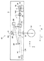
図2は、参考例に係る光ビーム走査装置10の副走査方向に沿った側面図(主走査方向に直角な方向から見た側面図)である。
【0072】
筐体11の内部には、矢印R方向側に、モータ12によって回転する多面鏡14を備える偏向器16が配置されている。本参考例では、多面鏡14の回転軸Cが鉛直方向であるが水平方向等の他の方向であっても勿論良い。
【0073】
偏向器16の矢印L方向側には、図3にも示すように、多面鏡14側から主走査方向(矢印Y方向)に曲率をもつ凹シリンドリカル面と平面で構成される第1のfθレンズ18と、同じく平面と主走査方向に曲率をもつ凸シリンドリカル面で構成される第2のfθレンズ20からなるfθレンズ系が配置されている。
【0074】
図2に示すように、第1のfθレンズ18及び第2のfθレンズ20は、多面鏡14の回転軸Cに対して直角とされた水平線HLに対して光軸が傾斜している。
【0075】
以下の表1に図3に示す光学系のレンズデータを示す。ここでは、rは曲率半径(mm)、dは中心間隔(mm)、nは屈折率を示す。
【0076】
【表1】

図2に示すように、第2のfθレンズ20の矢印L方向には、光ビームLBを出射する半導体レーザ等を含む光源22が配置されている。
【0078】
光源22から出射した光ビームLBは、水平線HLに対して斜め上方に角度αで第2のfθレンズ20、第1のfθレンズ18を透過して多面鏡14の偏向面14Aに入射する。
【0079】
偏向面14Aで反射した光ビームLBは、第1のfθレンズ18、第2のfθレンズ20を透過する。
【0080】
偏向面14Aで反射して第2のfθレンズ20を透過した光ビームLBと水平線HLとのなす角度はαとなる。なお、本参考例では、角度αが1.2°である。
【0081】
第2のfθレンズ20の矢印L方向側には、偏向面14Aで反射して第1のfθレンズ18、第2のfθレンズ20を透過した光ビームLBを矢印R方向側の斜め上方に向けて反射する平面ミラー24が配置されている。
【0082】
第2のfθレンズ20の上方にはシリンドリカルミラー26が配置されており、シリンドリカルミラー26は平面ミラー24で反射された光ビームLBを矢印L方向側の斜め上方に向けて反射する。
【0083】
シリンドリカルミラー26の光ビーム反射側には、平面ミラー28が配置されており、シリンドリカルミラー26で反射された光ビームLBを下方に配置された感光体30に向けて反射する。
【0084】
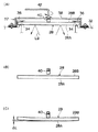
なお、筐体11の底面には、光ビームLBを通過させるために防塵ガラス31が設けられている。
【0085】
図4(A)に示すように、平面ミラー28は、主走査方向に長く形成されており、反射面28Aの両端部分が各々本体フレーム32に設けられた凸状の基準面34に板ばね36によって当て付けられ本体フレーム32に固定されている。
この本体フレーム32には、平面ミラー28を湾曲させるための平面鏡湾曲装置37が設けられている。
【0086】
平面鏡湾曲装置37は、ステー38及び調整ねじ40を備えている。
【0087】
ステー38は、平面ミラー28の背面28B側に配置され、屈曲した両端部分が板ばね36と共に本体フレーム32に固定されている。
【0088】
ステー38の中央には、平面ミラー28の背面28Bを押圧するための調整ねじ40が取り付けられている。
【0089】
平面ミラー28は、調整ねじ40によって長手方向中央部分を押圧されることによって反射面28Aが凸となるように湾曲する。
【0090】
なお、図2に示すように、筐体11の上壁には、調整ねじ40へのアクセスを可能とする孔41が形成されている。
(作用)
次に、参考例の作用を説明する。
【0091】
図2に示すように、光源22から出射した光ビームLBは、多面鏡14の回転軸Cに対して直角とされた水平線HLに対して副走査方向に角度αをなして第2のfθレンズ20、第1のfθレンズ18を透過し、走査範囲の中央方向から一定速度で回転する多面鏡14の偏向面14Aに入射する。
【0092】
光ビームLBは偏向面14Aで反射偏向され、第1のfθレンズ18、第2のfθレンズ20を通過する。
【0093】
ここで、水平先HLに対して副走査方向に角度αをなして入射し、また第1のfθレンズ18及び第2のfθレンズ20が傾斜しているので、多面鏡14で反射された光ビームLBは、感光体30の走査端に至る破線で示した光ビームLBが実線で示した光ビームLBに対して、水平線HLから離れる方向の走査線湾曲をもって偏向される(多面鏡14〜平面ミラー24の間)。
【0094】
第1のfθレンズ18、第2のfθレンズ20を透過した光ビームLBは、その後平面ミラー24により折り返され、シリンドリカルミラー26を経て平面ミラー28により折り返されて感光体30の表面にスポット状に結像されて主走査方向に走査される。
【0095】
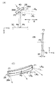
次に、図1にしたがって参考例の光路上における走査線湾曲を説明する。この図1は、平面鏡28での反射状態を示した図である。
【0096】
図1(A)に示すように、平面鏡28上では、主走査方向と直交する方向からみて、両走査端に至る光ビームLBe の反射点P1が、走査中心に至る光ビームLBcの反射点P2よりも光ビーム入射側(シリンドリカルミラー26側。矢印R方向側)にある。即ち、平面鏡28上では、走査線が光ビーム入射側とは反対側へ凸となる方向に湾曲している。
【0097】
図1(B)に示すように、感光体30上での走査線は、両走査端への光ビームLBe の入射点P3が、走査中心への光ビームLBcの入射点P4よりも、図2の配置構成においてはシリンドリカルミラー26側(矢印R方向側)にある。
【0098】
この状態で、図4(A)に示すように調整ねじ40を工具42で回し、図4(B)に示す平面状態から図4(C)に示すように平面鏡28の中央部を押し出す方向に調整すると、平面鏡28が反射面28Aが凸となるように湾曲し、これにより走査中心に至る光ビームLBc の平面鏡28上の反射点P2は、図1(A)に示す反射点P2'へと移動し、感光体30上の走査位置も、走査中心へ至る光ビームLBc が両走査端へ至る光ビームLBe と直線状となる位置に移動し、この結果、走査線湾曲は補正され、図の実線で示す湾曲した状態から2点鎖線で示す直線状へと補正される。
【0099】
次に、第1のfθレンズ18及び第2のfθレンズ20の作用を説明する。
【0100】
第1のfθレンズ18及び第2のfθレンズ20の傾き角βにより感光体30上の走査線の湾曲が変化する。参考例の構成(α=1.2°、β=6°。図2参照。)では、感光体30上の走査線の湾曲量ΔE(図1(B)参照)が約120μmである(平面鏡28の湾曲が無い状態。)。
【0101】
この湾曲量は、予めボウの製造時のばらつきよりも大きく設定されている。したがって、ばらつきを加味しても、感光体30上の走査線は必ず一定方向(平面鏡28の反射面28Aが凸となるように押し出したときに走査線が直線状になる方向)の湾曲となるので、調整ねじ40の押し出し方向(ねじ込み方向)のみの1方向調整機構で走査線湾曲を調整することができる。
【0102】
したがって、押し方向及び引き方向の双方向に平面ミラーを調整するタイプの調整機構に比較して走査線湾曲補正構造を簡略化することができる。また、平面湾曲手段が簡単な構成であるので、調整がずれる等の経時変化が起き難く、ボウ調整の維持性にも優れたものとなる。
【0103】
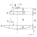
なお、図5は、第1のfθレンズ18及び第2のfθレンズ20の傾き角βと、平面鏡28上の走査線湾曲量、及び感光体30上の走査線湾曲量との関係を示した図である。
【0104】
ここで、傾き角βを負側(−側)にすると(図2とは反対側に傾斜。)、平面鏡28上の走査線湾曲方向は、感光体30上の走査線湾曲方向共に傾き角βを正にとった場合(図2の状態。)と反転する。
【0105】
図6は、第1のfθレンズ18及び第2のfθレンズ20の傾き角β(図6では図示せず。)を入射光ビームとなす角が小さくなる方向に傾けたとき(即ち、図2とは反対側に傾斜したとき。)の光ビームの光路を示した図である。
【0106】
図6の状態で背面28Bから平面鏡28の中央部分を押し出すと、走査中心の光ビームLBc は、2点鎖線で示すように走査端の光ビームLBe から離れる方向に移動し、走査線湾曲が大きくなってしまう。したがって、走査線の湾曲を補正するには、平面鏡28を背面側に引く機構が必要となり、平面鏡を押し引きする従来の機構と同一の構成となってしまい構成が複雑となる。
【0107】
したがって、構成を簡単にするには第1のfθレンズ18及び第2のfθレンズ20を傾斜する方向は、その光軸が偏向面14Aの法線に対して偏向器16へ入射する光ビームとは反対方向に傾斜するように傾斜配置することが好ましいのである。
【0108】
また、第1のfθレンズ18及び第2のfθレンズ20の傾斜方向は、参考例のようなダブルパス正面入射の構成では、レンズ表面からの戻り光防止、主走査方向のビーム径の均一性を向上させる方向とも一致する方向である。
【0109】
また、平面ミラー28の背面28B側に平面鏡湾曲装置37が設けられ、平面ミラー28の背面28B側が筐体11の一側の平面に面しているので、他の光学部材等に干渉されず平面鏡湾曲装置37へのアクセスが容易である。
[実施形態]
次に、本発明の実施形態を図7にしたがって説明する。なお、参考例と同一構成には同一符号を付し、その説明は省略する。
【0110】
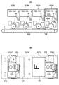
図7に示す光ビーム走査装置50は、ブラック(K)、イエロー(Y)、マゼンタ(M)、シアン(C)の4色を重ね合わせてフルカラー画像を形成するためのフルカラー画像形成装置に用いるものである。
【0111】
本実施形態の光ビーム走査装置50は、参考例の光ビーム走査装置10の光学系を、偏向器16を挟んで対称的に配置したものを基本とし、更に反射ミラー、光源等を追加したものであり、4つの光源52から発せられた光ビームLB1 〜LB4 を多面鏡14の回転軸を挟んで回転軸と直交する両方向から2組のfθレンズ20,18を透過させて、単一の多面鏡14の対向する2面に各2本づつ上下方向に角度を異ならせて入射させ、偏向後に再びfθレンズ18,20を透過した光ビームを光路分割して4つの感光体30K,30Y,30M,30Cに導くものである。
【0112】
感光体30Kに形成されたブラックの画像、感光体30Yに形成されたイエローの画像、感光体30Mに形成されたマゼンタの画像及び感光体30Cに形成されたシアンの画像を一定の速度で一方向(例えば矢印L方向)に搬送される中間転写体(図示せず)に順次転写したのち、一括して用紙に転写することによりカラーの画像が得られる。なお、このように、4つの感光体によってカラー画像を得る多色画像形成装置の構成(光ビーム走査装置を除く)については一般的に知られている構成であるため、詳しい説明は省略する。
【0113】
ここで、この光ビーム走査装置50では、偏向器16の矢印L方向側の光学系と矢印R方向側の光学系とは対称な構成であるため、矢印L方向側の光路に沿って詳細に説明を行う。
【0114】
半導体レーザ54から出射した発散状態の光ビームLB1 は、カップリングレンズ56により緩やかな発散光束とされ、スリット58により光ビームの光束幅を規制されたのち、シリンドリカルレンズ60により副走査方向にのみ収束作用を受ける。
【0115】
合成ミラー62により折り返された光ビームLB1 は、合成ミラー62の上部を通過する他の半導体レーザ54からの光ビームLB2 と、主走査断面でほぼ同一に光路を通る光ビームに合成される。
【0116】
合成された2本の光ビームLB1 ,LB2 は、正面入射用の単一の折返ミラー63a(偏向器16を挟んで反対側には対称的に折返ミラー63bが配置されている。)により折り返されて、副走査断面で入射角度の異なる2本の光ビームLB1 ,LB2 としてfθレンズ20、18を透過して単一の多面鏡14に入射する。
【0117】
多面鏡14への副走査方向入射角度の違いと、多面鏡14の偏向面14A上の2本の光ビームLB1 ,LB2 の反射位置を回転軸Cと平行方向に離間することにより、多面鏡14から離れるにしたがって光線間隔が広がる2本の光ビームLB1 ,LB2 として偏向される。
【0118】
この2本の偏向光ビームLB1 ,LB2 は、図1と同様に、各々走査中心に至る光ビームに対して、両走査端に至る光ビームが図7の上側に位置する走査線湾曲を持っている。
【0119】
fθレンズ18,20を透過した2本の光ビームLB1 ,LB2 は、除々にその副走査方向の光線間隔を広げて進み、光ビームLB1 は、折返ミラー64Aの上部を通過し、その後方に配設された折返ミラー64Bにより、それぞれの光路上に設けられたシリンドリカルミラー66A,66Bに入射する。
【0120】
シリンドリカルミラー66A,66Bにより反射された光ビームLB1 ,LB2 は、それぞれの光路上に独立に設けられた平面鏡68A,68Bにより折り返されて防塵ガラス70A,70Bを透過したのち、感光体30A,30B上にスポット結像される。
【0121】
平面鏡68A,68Bの反射面の反対側には、参考例と同様の平面鏡湾曲装置37(図7では調整ねじ40のみ図示。)がそれぞれ設けられている。
【0122】
また、2本の光ビームLB1 ,LB2 の光路は、副走査断面内で多面鏡14の偏向面14Aと感光体30A,30Bがそれぞれ幾何光学的に共役関係となる面倒れ補正光学系を構成している。
【0123】
双方向走査の対向面側は、多面鏡14の回転軸Cを含み、感光体30の母線を含む平面に対して面対称の構成となっており、上記した2本の光ビームLB1 ,LB2 と同様の光路を通る。
【0124】
但し、本実施形態では、単一の多面鏡14の対向する2面により偏向走査するため、感光体30の走査方向は双方向を走査する各2本づつ逆向きとなる。
【0125】
このため、画像データを反転する必要があるが、双方向走査の画像データ処理方法の詳細は本発明とは直線関係がないので説明を省略する。
【0126】
以下に本実施形態の基本パラメータを示す。
(1)fθレンズへ入射する光ビームの副走査方向の入射角度・・・・・・・・・・・・・・・・1.2°及び2.5°(α)
(2)fθレンズ
レンズデータ・・・・・・・・・・参考例と同一(表1参照)
偏向角・・・・・・・・・・・・・±12.8°(走査幅297mmに対応) 傾け角β・・・・・・・・・・・・6°
(3)多面鏡
内接円半径・・・・・・・・・・・12.5mm
面数・・・・・・・・・・・・・・12面
偏向面上の2ビーム間距離・・・・3.5mm
(4)イニシャルボウ(湾曲量)・・・・・119μm(1.2°入射の光ビーム) 122μm(2.5°入射の光ビーム) この実施形態に示した構成では、半導体レーザ54からの発散光をカップリングレンズ56によって緩やかな発散光とし、fθレンズ20,18により主走査方向の平行光束として多面鏡14に入射する。
【0127】
この平行光束の幅(主走査方向に対応した幅)は、多面鏡14の面幅(主走査方向に対応した幅)よりも広く、所謂オーバーフィールド光学系となっている。
【0128】
この構成とすることにより、多面鏡14を小型化(小径化)することができ、多面鏡14を回転させるモータ(図示せず)の負荷を軽減し、高速化、高解像化に適した光ビーム走査装置として構成できる。
【0129】
平面鏡湾曲装置37は、参考例と同じく図4に示す構成のものを使用することができる。
【0130】
光ビーム走査装置50の製造時には、感光体30A〜Dに対応する位置に光ビーム位置検出センサを設けた治具の上に光ビーム走査装置50を載せ、調整ねじ40を工具42により回して押し込むことにより、平面鏡68A〜Dに押圧をかけない状態で約120μmあった走査線湾曲をほぼ直線状となるように調整する。
【0131】
この実施形態における被走査面上(感光体30A〜D上)の走査線湾曲を補正するために必要な平面鏡68A〜Dの押込み量は、260mmスパンで80μm程度であり、平面鏡68A〜Dが破壊する虞れはない。
【0132】
また、イニシャルボウ、調整量共に多面鏡14への入射角度の異なる二つの光ビームLB1 ,LB2 でほぼ同量となっているので、平面鏡68A〜Dの湾曲による倍率変動はあるが、リニアリティ(走査位置誤差)は略同じ傾向で変化するので、部分的な色ずれは生じにくい。
【0133】
なお、倍率変動は、前述したように画像信号の駆動周波数を変化させる電気的な手段により補正可能である。
【0134】
画像形成装置上で走査湾曲を補正する場合、走査線湾曲量を正確に計測することは不可能なので、調整前状態でプリントサンプルを取り、平面鏡湾曲装置37の調整ねじ40が最も押込み側にある光ビームを選択し、残りの光ビームの光路上に設けられた平面鏡湾曲装置37の調整ねじ40を調整して、選択した基準色(調整ねじ40が最も押込み側にある光ビームによる。)との差が小さくなる方向に調整することで、比較的容易に色ずれを補正することができる。
【0135】
なお、この光ビーム走査装置50は、図示しない筐体内に設けられており、この筐体には、調整ねじ40へのアクセスを可能とする孔(図示せず)が各調整ねじ40の近傍の壁面に設けられている。
【0136】
【発明の効果】
以上説明したように、本発明の光ビーム走査装置は上記の構成としたので、簡素な補正機構で被走査面上の走査線湾曲を補正することができる、という優れた効果を有する。
【図面の簡単な説明】
【図1】 (A)は参考例に係る光ビーム光学走査装置の平面鏡の反射状態を示した主走査方向に沿って見た側面図であり、(B)は被走査面上での走査線を示す図であり、(C)は平面鏡の反射状態を示した斜視図である。
【図2】 参考例に係る光ビーム光学走査装置の主走査方向に沿って見た側面図である。
【図3】 2枚構成のfθレンズ及び平面鏡近傍の光学系の平面図である。
【図4】 (A)は平面鏡湾曲手段の側面図であり、(B)は調整前の平面鏡を示す平面鏡の側面図であり、(C)は調整後の平面鏡を示す平面鏡の側面図である。
【図5】 fθレンズの傾き角β、平面鏡上の走査線湾曲量及び被走査面上の走査線湾曲量との関係を示したグラフである。
【図6】 fθレンズを入射光ビームとなす角が小さくなる方向に傾けたときの光ビームの光路を示した図である。
【図7】 本発明の光ビーム走査装置の実施形態を示す斜視図である。
【図8】 光ビーム走査装置による被走査面上の走査線レジストレーションを分類して示した説明図である。
【図9】 ボウの湾曲方向を説明するための説明図である。
【図10】 (A)は4個の画像形成部を直列に配置したフルカラー画像形成装置の概略構成を示す側面図であり、(B)はその平面図である。
【符号の説明】
10 光ビーム走査装置
11 筐体
14 多面鏡
14A 偏向面
16 偏向器
18 fθレンズ(結像光学系)
20 fθレンズ(結像光学系)
22 光源
26 シリンドリカルミラー(結像光学系)
28 平面鏡
30 感光体(被走査面)
37 平面鏡湾曲装置(平面鏡湾曲手段)
50 光ビーム走査装置
52 光源[0001]
BACKGROUND OF THE INVENTION
In the present invention, a light beam emitted from a laser light source is deflected by a deflector such as a polygon mirror, imaged in a spot shape on a scanned surface by an imaging optical system, and scanned linearly at a constant speed. More particularly, the present invention relates to a beam scanning device. More specifically, a scanning curve is given to an incident light beam on a plane mirror provided between an imaging optical system and a surface to be scanned in advance, and the bending direction and the folding direction of the plane mirror have a specific relationship. Thus, the present invention relates to a light beam scanning apparatus capable of correcting the scanning line curvature on the surface to be scanned with simple correction.
[0002]
[Prior art]
Conventionally, a light beam emitted from a laser light source is deflected by a deflector such as a polygon mirror, and is imaged in a spot shape by an imaging optical system including an fθ lens, and the surface to be scanned is scanned at a constant speed. A beam scanning apparatus and an image forming apparatus that uses the light beam scanning apparatus as an exposure source to form a latent image on a photosensitive member and develop and transfer the latent image by an electrophotographic process are used. The demand for higher speed and higher image quality has increased rapidly in recent years.
[0003]
In order to respond to higher speed, the rotation of the drive motor of the deflector is increased, and multiple beam writing is performed by a multi-beam light source. To cope with higher image quality, the writing density is increased and the beam diameter is increased. It has been done to make it smaller. Furthermore, in order to achieve high image quality, it is also required to improve the accuracy of scanning line registration.
[0004]
FIG. 8 is a diagram in which the scanning line registration on the surface to be scanned by the light beam scanning device is classified.
[0005]
In FIG. 8, a solid line represents a scanning line, and a broken line represents a scanning line having an error.
[0006]
As described above, the registration misalignment affecting image quality is classified into five categories: (a) lead registration misalignment, (b) side registration misalignment, (c) magnification misalignment, (d) inclination (skew), and (e) bending (bow). The
[0007]
Among these, (a) lead registration error, (b) side registration error, (c) magnification error, and (d) inclination (skew) are the adjustment of the relative positional relationship between the light beam scanning device and the surface to be scanned and the light. It can be adjusted by two methods of adjusting the light beam emitted from the beam scanning device.
[0008]
For example, in the case of (c) magnification shift, the relative distance between the light beam scanning device and the light beam scanning surface may be adjusted, or the frequency of the image signal may be adjusted. As another adjustment method of the emitted light beam, it is also possible to adjust the position and the curved state of the optical component provided in the light beam scanning apparatus.
[0009]
However, (e) bending (bow) does not change substantially even if the relative relationship between the light beam scanning device and the surface to be scanned is adjusted. Therefore, it is necessary to adjust the light beam itself emitted from the light beam scanning device. There is. For this reason, bow adjustment is performed at the time of manufacturing the light beam scanning apparatus, and this initial adjustment state is maintained even after being mounted on the image forming apparatus.
[0010]
The cause of the bow is mainly the processing error of the optical components mounted on the light beam scanning device and the assembly error of the light beam scanning device to the housing, which depends on the device configuration and the number of optical components arranged on the optical path. However, the variation between the devices without adjustment is usually about 0.1 mm.
[0011]
Here, in order to discuss the size of the bow, the bending direction must be considered.
[0012]
FIG. 9 is a view for explaining the bending direction of the bow. For convenience, the upward convex case is positive (plus), and the downward convex case is negative (−).
[0013]
The above-described bow size of 0.1 mm is a size (pp) in consideration of this sign. If the average bow amount of bow is substantially zero, the irregularity is ± 0.05 mm.
[0014]
Up to this point, one scanning line has been described. Next, the case of full-color image formation using a plurality of scanning lines will be described.
[0015]
With the widespread use of color originals and color images, the above-described high speed and high image quality are also required for color image forming apparatuses. In recent years, full-color image output is required at the same speed as single-color image forming apparatuses. However, the conventional popular color image forming apparatus includes a single light beam scanning device, and sequentially performs exposure, development, and transfer processes on a single photoconductor, and fixes them on these sheets. Since the process of forming an image is taken, for example, when four colors of black (K), yellow (Y), magenta (M), and cyan (C) are superimposed, a fixed image is obtained after the process is repeated four times. Is output, the image output speed is ¼ that of a single color, and there is a limit to how to deal with the increase in speed.
[0016]
Therefore, as a technique for obtaining an image output speed similar to that of a single-color image forming apparatus, a plurality of independent image forming units are provided, and the developed image formed here is continuously transferred to a single transfer medium in one cycle. So-called tandem image forming apparatuses that form full-color images have been developed.
[0017]
10A and 10B are diagrams illustrating a schematic configuration of a full-color image forming apparatus in which four image forming units are arranged in series.
[0018]
As shown in FIGS. 10A and 10B, the
[0019]
After charging the
[0020]
Next, after the latent image is developed by the developing
[0021]
This process is performed in the order of black, yellow, magenta, and cyan, and the transfer image is fixed on the
[0022]
In such an image forming apparatus in which a plurality of image forming units are connected, the light beam from the light
[0023]
Against this background, various bow correction methods have been proposed in order to achieve high image quality of single-color images and to achieve high image quality of full-color images.
[0024]
For example, Japanese Patent Application Laid-Open No. 5-34612 discloses a long cylindrical lens provided in an optical path that includes a curvature amount adjusting unit that changes the degree of curvature in a plane substantially perpendicular to the optical path. Yes.
[0025]
Japanese Patent Application Laid-Open No. 2-28916 discloses that a beam scanning line formed on a scanning surface is deformed by bending a plane mirror.
[0026]
Japanese Patent Application Laid-Open No. 4-264417 discloses a device provided with a curved surface forming means for irradiating a photosensitive member with a laser beam via a mirror and bending the mirror.
[0027]
Further, in JP-A-8-146325, a flat reflecting mirror is previously curved by a pressing means so that the reflecting surface has a concave shape, and the convex side of the flat reflecting mirror is pressed by another pressing means. In this figure, the correction of the curvature of the scanning line is shown.
[0028]
[Problems to be solved by the invention]
However, as disclosed in Japanese Patent Laid-Open No. 5-34612, in order to bend the optical component in a direction substantially perpendicular to the optical path, the short side of the rectangular cross-sectional shape must be pressed, and the viewpoint of ease of bending Therefore, in reality, plastic lenses must be used. When a glass lens is used dare, there is a problem that the adjustment amount is limited in order to avoid the destruction.
[0029]
In the example shown in Japanese Patent Laid-Open No. 2-2916, in order to correct the scanning line curvature in both directions as shown in FIG. It can be said that the mechanism is complicated and expensive, and the maintainability after mounting the image forming apparatus is inferior due to the large number of parts.
[0030]
In the example shown in Japanese Patent Application Laid-Open No. 4-264417, the mirror is curved by the piezoelectric element, so it must be expensive. Further, when using a push screw or a cam, a mechanism for warping both concaves and convexes must be provided, as in JP-A-2-28916, and the mechanism becomes complicated and expensive, and after the image forming apparatus is mounted. In terms of maintainability, it can be said that the number of parts is inferior.
[0031]
In the example shown in Japanese Patent Application Laid-Open No. 8-146325, it is possible to correct the scanning line curvature in both directions as shown in FIG. 9, but the first and second pressing means are necessary. Becomes complicated.
[0032]
The present invention has been made in view of such a problem, and a first object of the present invention is to provide a light beam scanning apparatus capable of correcting the scanning line curvature on the surface to be scanned with a simple correction mechanism.
[0033]
Further, it is possible to provide a light beam scanning device for a full-color image forming apparatus capable of correcting the curvature of the scanning line on the light beam scanning surface with a simple correction mechanism and correcting the color shift between the plurality of scanning lines. The second purpose.
[0034]
[Means for Solving the Problems]
The invention described in claim 1A single deflector that simultaneously scans a plurality of light beams by a single deflector, and a plurality of photosensitive members that are irradiated with the light beams scanned by the deflector, the same deflection of the deflector A plurality of light beams are incident on the surface in the same direction with respect to the main scanning direction and at an angle different from each other in the sub-scanning direction, and a scanning curve is caused by the rotation of the deflector. After forming a deflected beam and passing the deflected beam through an fθ lens whose optical axis is inclined in the sub-scanning direction, the optical path is turned back by a plane mirror having a mechanism for adjusting the amount of bending in the main scanning direction. In the full-color light beam scanning apparatus that scans the light beam, the incident angle of the light beam in the sub-scanning direction on the deflection surface and the tilt angle of the fθ lens are the same as the scanning on all the photoconductors when the plane mirror is not adjusted. The amount of wire bending is made It is set to be a bending direction in which the scanning line bending can be reduced by adjusting the mechanism for adjusting the bending amount in the main scanning direction in one direction, which is greater than the manufacturing variation.It is characterized by that.
[0035]
The operation of the light beam scanning apparatus according to
[0036]
A plurality of light beams are deflected in the main scanning direction by being reflected by the same deflecting surface of a single deflector. The light beam then scans the photoreceptor.here,A deflected beam having a scanning curve by rotating a deflector by causing a plurality of light beams to enter the same direction with respect to the main scanning direction and at an angle different from each other in the sub-scanning direction. Can be formed. Then, after passing this deflected beam through an fθ lens whose optical axis is inclined in the sub-scanning direction, the optical path is turned back by a plane mirror provided with a mechanism for adjusting the amount of bending in the main scanning direction, and the photosensitive member is scanned. In addition,The scanning line bending amount is previously set larger than the manufacturing variation of the bow.
[0037]
[0038]
[0039]
[0040]
In this way, the amount of curvature of the scanning line (initial bow determined by the optical design) when the flat mirror is in an unadjusted state is set to be larger than the manufacturing variation of the bow, so the amount of curvature in the main scanning direction is adjusted. It is possible to make the mechanism to perform a simple configuration. In addition, by making the mechanism simple, the maintenance of bow adjustment is excellent.
In addition, since the plurality of light beams are incident on the deflecting surface at different angles in the sub-scanning direction, both the optical path of the light beam incident on the deflector and the optical path of the scanning light beam deflected by the deflector are special. It is possible to synthesize and separate light beams without using an optical element.
In addition, a plane mirror that folds back the corresponding light beam on each optical path of a plurality of light beams. By providing, the scanning line curvature on the surface to be scanned of a plurality of light beams can be adjusted independently.
[0041]
The invention described in
[0042]
The operation of the light beam scanning apparatus according to
[0043]
The light beam scanning device according to
By a mechanism for adjusting the amount of bending of the flat mirror in the main scanning direction, the scanning line is reduced by pushing the flat mirror from the opposite side of the reflecting surface.
[0044]
[0045]
[0046]
In this state,By a mechanism that adjusts the amount of curvature of the flat mirror in the main scanning direction, for example,When the substantially central portion of the plane mirror in the main scanning direction is pushed out from the surface opposite to the surface on which the light beam is incident (that is, the back surface), the plane mirror is curved so that the surface on which the light beam is incident is convex. The reflection point of the light beam reaching the scanning center of the plane mirror can be moved to the front side of the optical path, and the curvature of the scanning line on the surface to be scanned can be corrected.
[0047]
Here, when the plane mirror is extruded and curved as described above, the curvature of the incident light beam projected on the reflection surface of the plane mirror and the scan line curve on the scanned surface are predetermined in advance, that is, the central portion of the plane mirror. Can be folded back in a direction in which the scanning line on the scanned surface approaches a straight line.
[0048]
Therefore,No adjustmentThat is, since the scanning line bending amount (initial bow determined by the optical design) in a state where the plane mirror is not curved is taken larger than the manufacturing variation of the bow,Mechanism for adjusting the amount of curvature of the plane mirror in the main scanning directionNeed only have an adjustment function for the direction of extrusion,Mechanism for adjusting the amount of curvature of the plane mirror in the main scanning directionCan be configured in a simple manner. Also,Mechanism for adjusting the amount of curvature of the plane mirror in the main scanning directionBy adopting a simple configuration, the maintenance of bow adjustment is excellent.
[0049]
The invention according to claim 33. The light beam scanning apparatus according to
[0050]
The operation of the light beam scanning apparatus according to
The imaging optical system here refers to a portion constituted by an optical component having an optical refractive index in the main scanning direction or the sub-scanning direction, and both the main scanning direction and the sub-scanning direction.
In the light beam scanning device according to
[0051]
[0052]
[0053]
[0054]
[0055]
[0056]
[0057]
[0058]
[0059]
[0060]
[0061]
[0062]
[0063]
[0064]
[0065]
[0066]
[0067]
[0068]
[0069]
[0070]
DETAILED DESCRIPTION OF THE INVENTION
[Reference example]
Before describing the light beam scanning apparatus of the present invention, a light beam scanning apparatus according to a reference example.Will be described with reference to FIGS.
[0071]
FIG.Reference exampleIt is a side view along the sub-scanning direction of the light beam scanning apparatus according to FIG.
[0072]
Inside the
[0073]
On the arrow L direction side of the
[0074]
As shown in FIG. 2, the optical axes of the
[0075]
Table 1 below shows lens data of the optical system shown in FIG. Here, r is a radius of curvature (mm), d is a center interval (mm), and n is a refractive index.
[0076]
[Table 1]
As shown in FIG. 2, a
[0078]
The light beam LB emitted from the
[0079]
The light beam LB reflected by the deflecting
[0080]
The angle between the light beam LB reflected by the deflecting
[0081]
On the arrow L direction side of the
[0082]
A
[0083]
A
[0084]
A
[0085]
As shown in FIG. 4A, the
The main body frame 32 is provided with a plane
[0086]
The plane
[0087]
The
[0088]
An
[0089]
The
[0090]
As shown in FIG. 2, a
(Function)
next,Reference exampleThe operation of will be described.
[0091]
As shown in FIG. 2, the light beam LB emitted from the
[0092]
The light beam LB is reflected and deflected by the deflecting
[0093]
Here, the light incident on the horizontal tip HL at an angle α in the sub-scanning direction and the
[0094]
The light beam LB transmitted through the
[0095]
Next, according to FIG.Reference exampleThe scanning line curve on the optical path will be described. FIG. 1 is a diagram showing a state of reflection by the
[0096]
As shown in FIG. 1A, on the
[0097]
As shown in FIG. 1B, the scanning line on the
[0098]
In this state, the
[0099]
Next, the operation of the
[0100]
The curve of the scanning line on the photoconductor 30 changes depending on the inclination angle β of the
[0101]
This amount of bending is set in advance to be larger than the variation at the time of manufacturing the bow. Therefore, even if the variation is taken into account, the scanning line on the
[0102]
Therefore, the scanning line curvature correction structure can be simplified as compared with an adjustment mechanism of a type that adjusts the plane mirror in both the pushing direction and the pulling direction. In addition, since the plane bending means has a simple configuration, it is difficult to cause a change with time such as a shift in adjustment, and the bow adjustment maintainability is excellent.
[0103]
FIG. 5 shows the relationship between the inclination angle β of the
[0104]
Here, when the inclination angle β is set to the negative side (− side) (inclination to the opposite side to FIG. 2), the scanning line bending direction on the
[0105]
6 shows a case where the tilt angle β (not shown in FIG. 6) of the
[0106]
When the central portion of the
[0107]
Therefore, in order to simplify the configuration, the
[0108]
The tilt directions of the
[0109]
In addition, since the plane
[Embodiment]
Next, an embodiment of the present inventionWill be described with reference to FIG. In addition,Reference exampleThe same components as those in FIG.
[0110]
The light beam scanning apparatus 50 shown in FIG. 7 is used in a full-color image forming apparatus for superposing four colors of black (K), yellow (Y), magenta (M), and cyan (C) to form a full-color image. Is.
[0111]
The light beam scanning apparatus 50 of this embodiment isReference exampleThe optical system of the optical
[0112]
The black image formed on the photoconductor 30K, the yellow image formed on the photoconductor 30Y, the magenta image formed on the photoconductor 30M, and the cyan image formed on the
[0113]
Here, in this light beam scanning device 50, the optical system on the arrow L direction side and the optical system on the arrow R direction side of the
[0114]
The divergent light beam LB1 emitted from the semiconductor laser 54 is changed into a gentle divergent light beam by the
[0115]
The light beam LB1 turned back by the combining
[0116]
The two combined light beams LB1 and LB2 are folded back by a single folding mirror 63a for front incidence (a
[0117]
The angle of the sub-scanning direction incident on the
[0118]
The two deflected light beams LB1 and LB2 have a scanning line curve in which the light beams reaching both scanning ends are located on the upper side of FIG. Yes.
[0119]
The two light beams LB1 and LB2 that have passed through the
[0120]
The light beams LB1 and LB2 reflected by the cylindrical mirrors 66A and 66B are folded by the plane mirrors 68A and 68B independently provided on the respective optical paths, pass through the dust-
[0121]
On the opposite side of the reflecting surfaces of the plane mirrors 68A and 68B,Reference exampleThe same plane mirror bending device 37 (only the
[0122]
The optical paths of the two light beams LB1 and LB2 constitute a surface tilt correction optical system in which the deflecting
[0123]
The opposite surface side of the bidirectional scanning includes the rotation axis C of the
[0124]
However, in this embodiment, since scanning is deflected by two opposing surfaces of the single
[0125]
For this reason, it is necessary to invert the image data. However, the details of the image data processing method for bidirectional scanning are not linearly related to the present invention, and the description thereof is omitted.
[0126]
less thanThis embodimentThe basic parameters of
(1) Incident angle of the light beam incident on the fθ lens in the sub-scanning direction ... 1.2 ° and 2.5 ° (α)
(2) fθ lens
Lens dataReference example(See Table 1)
Deflection angle: ± 12.8 ° (corresponding to scanning width of 297mm) Tilt angle β: 6 °
(3) Polyhedral mirror
Inscribed circle radius ... 12.5mm
Number of faces ... 12
Distance between two beams on the deflection surface ... 3.5mm
(4) Initial bow (bending amount): 119 μm (light beam with 1.2 ° incidence) 122 μm (light beam with 2.5 ° incidence)EmbodimentIn the configuration shown in FIG. 2, divergent light from the semiconductor laser 54 is made gentle divergent light by the
[0127]
The width of the parallel light beam (width corresponding to the main scanning direction) is wider than the surface width of the polygon mirror 14 (width corresponding to the main scanning direction), which is a so-called overfield optical system.
[0128]
With this configuration, the
[0129]
The plane
[0130]
At the time of manufacturing the light beam scanning device 50, the light beam scanning device 50 is placed on a jig provided with a light beam position detection sensor at a position corresponding to the
[0131]
In this embodiment, the pushing amount of the plane mirrors 68A to 68D required for correcting the scanning line curvature on the scanned surface (on the
[0132]
Further, since the initial bow and the adjustment amount are almost the same in the two light beams LB1 and LB2 having different incident angles to the
[0133]
Note that the magnification variation can be corrected by an electric means for changing the drive frequency of the image signal as described above.
[0134]
When the scanning curve is corrected on the image forming apparatus, it is impossible to accurately measure the scanning line curve amount. Therefore, the print sample is taken in the state before adjustment, and the
[0135]
The light beam scanning device 50 is provided in a housing (not shown), and a hole (not shown) that allows access to the adjusting
[0136]
【The invention's effect】
As described above, since the light beam scanning apparatus of the present invention has the above-described configuration, it has an excellent effect that the scanning line curvature on the surface to be scanned can be corrected with a simple correction mechanism.
[Brief description of the drawings]
FIG. 1 (A) isReference exampleFIG. 5B is a side view seen along the main scanning direction showing the reflection state of the plane mirror of the light beam optical scanning device according to FIG. 6B, FIG. 5B is a diagram showing scanning lines on the surface to be scanned, and FIG. It is the perspective view which showed the reflective state of the plane mirror.
[Figure 2]Reference exampleIt is the side view seen along the main scanning direction of the light beam optical scanning device concerning.
FIG. 3 is a plan view of an optical system in the vicinity of a two-element fθ lens and a plane mirror.
4A is a side view of the plane mirror bending means, FIG. 4B is a side view of the plane mirror showing the plane mirror before adjustment, and FIG. 4C is a side view of the plane mirror showing the plane mirror after adjustment. .
FIG. 5 is a graph showing a relationship among an inclination angle β of an fθ lens, a scanning line bending amount on a plane mirror, and a scanning line bending amount on a scanned surface.
FIG. 6 is a diagram illustrating an optical path of a light beam when an fθ lens is tilted in a direction in which an angle formed by an incident light beam is reduced.
FIG. 7 shows a light beam scanning apparatus according to the present invention.EmbodimentFIG.
FIG. 8 is an explanatory diagram showing classification of scanning line registration on a surface to be scanned by the light beam scanning device.
FIG. 9 is an explanatory diagram for explaining a bending direction of a bow.
10A is a side view showing a schematic configuration of a full-color image forming apparatus in which four image forming units are arranged in series, and FIG. 10B is a plan view thereof.
[Explanation of symbols]
10 Light beam scanning device
11 Case
14 polygon mirror
14A deflection surface
16 Deflector
18 fθ lens (imaging optical system)
20 fθ lens (imaging optical system)
22 Light source
26 Cylindrical mirror (imaging optical system)
28 Plane mirror
30 photoconductor (scanned surface)
37 Plane mirror bending device (plane mirror bending means)
50 Light beam scanning device
52 Light source
Claims (3)
前記偏向器の同一の偏向面に対し、主走査方向に対しては同一方向で、かつ副走査方向には角度を持たせて相互に異なる角度で複数の光ビームを入射させ、前記偏向器の回転により走査湾曲を持った偏向ビームを形成し、
前記偏向ビームを副走査方向に光軸を傾けたfθレンズを通過させた後、主走査方向の湾曲量を調整する機構を備えた平面ミラーにより光路を折り返して感光体上を走査するフルカラー用の光ビーム走査装置において、
前記偏向面への副走査方向光ビーム入射角度と、fθレンズの傾け角度は、前記平面ミラーが無調整状態においては全ての前記感光体上の走査線湾曲量が製造ばらつき以上となり、前記主走査方向の湾曲量を調整する機構を一方向に調整することで走査線湾曲が減少可能な湾曲方向となるように設定されている、ことを特徴とする光ビーム走査装置。 A single deflector that simultaneously scans a plurality of light beams with a single deflector, and a plurality of photoreceptors that are irradiated with the light beams scanned by the deflector,
A plurality of light beams are incident on the same deflecting surface of the deflector in the same direction with respect to the main scanning direction and at an angle different from each other with an angle in the sub-scanning direction. By forming a deflected beam with scanning curvature by rotation,
After passing the deflected beam through an fθ lens whose optical axis is inclined in the sub-scanning direction, the optical path is turned back by a plane mirror having a mechanism for adjusting the amount of curvature in the main scanning direction, and the photosensitive member is scanned on the photoconductor. In a light beam scanning device,
The incident angle of the light beam in the sub-scanning direction on the deflection surface and the tilt angle of the fθ lens are such that when the plane mirror is not adjusted, the amount of scanning line curvature on all the photoconductors exceeds the manufacturing variation, and the main scanning is performed. A light beam scanning apparatus characterized in that a scanning line curvature is set to be reduced by adjusting a mechanism for adjusting a bending amount of the direction in one direction .
平面ミラーの主走査方向の湾曲量を調整する機構は、反射面反対側から押し出す方向である、ことを特徴とする請求項1に記載の光ビーム走査装置。The light beam scanning apparatus according to claim 1, wherein the mechanism for adjusting the amount of curvature of the flat mirror in the main scanning direction is a direction of pushing out from the opposite side of the reflecting surface.
各々の結像光学系に2本づつ光ビームを走査する、ことを特徴とする請求項1または請求項2に記載の光ビーム走査装置。The light beam scanning apparatus according to claim 1, wherein two light beams are scanned on each imaging optical system.
Priority Applications (1)
| Application Number | Priority Date | Filing Date | Title |
|---|---|---|---|
| JP36114198A JP3709727B2 (en) | 1998-12-18 | 1998-12-18 | Optical beam scanning device |
Applications Claiming Priority (1)
| Application Number | Priority Date | Filing Date | Title |
|---|---|---|---|
| JP36114198A JP3709727B2 (en) | 1998-12-18 | 1998-12-18 | Optical beam scanning device |
Publications (2)
| Publication Number | Publication Date |
|---|---|
| JP2000180778A JP2000180778A (en) | 2000-06-30 |
| JP3709727B2 true JP3709727B2 (en) | 2005-10-26 |
Family
ID=18472368
Family Applications (1)
| Application Number | Title | Priority Date | Filing Date |
|---|---|---|---|
| JP36114198A Expired - Fee Related JP3709727B2 (en) | 1998-12-18 | 1998-12-18 | Optical beam scanning device |
Country Status (1)
| Country | Link |
|---|---|
| JP (1) | JP3709727B2 (en) |
Families Citing this family (6)
| Publication number | Priority date | Publication date | Assignee | Title |
|---|---|---|---|---|
| JP4537285B2 (en) | 2004-07-29 | 2010-09-01 | キヤノン株式会社 | Optical scanning apparatus having scanning line curvature correction mechanism |
| JP4500633B2 (en) * | 2004-09-07 | 2010-07-14 | キヤノン株式会社 | Optical scanning device and image forming apparatus using the same |
| US20070029471A1 (en) * | 2005-08-05 | 2007-02-08 | Kabushiki Kaisha Toshiba | Optical beam scanning device and image forming apparatus |
| JP5354323B2 (en) * | 2007-07-02 | 2013-11-27 | 株式会社リコー | Optical scanning apparatus and image forming apparatus |
| JP5207132B2 (en) * | 2008-10-20 | 2013-06-12 | 株式会社リコー | Optical scanning apparatus and image forming apparatus |
| WO2015194284A1 (en) * | 2014-06-20 | 2015-12-23 | 京セラドキュメントソリューションズ株式会社 | Optical scanning device and image formation device provided therewith |
-
1998
- 1998-12-18 JP JP36114198A patent/JP3709727B2/en not_active Expired - Fee Related
Also Published As
| Publication number | Publication date |
|---|---|
| JP2000180778A (en) | 2000-06-30 |
Similar Documents
| Publication | Publication Date | Title |
|---|---|---|
| US8077193B2 (en) | Optical scanning device and image forming apparatus using the same | |
| US8553061B2 (en) | Optical scanning device and image forming apparatus using the same | |
| JP3397822B2 (en) | Image forming system | |
| US8217980B2 (en) | Multi-beam optical scanning device and image forming apparatus using the same | |
| JP2008281945A (en) | Optical scanning apparatus and image forming apparatus | |
| US7768542B2 (en) | Multi-beam optical scanning device and image forming apparatus using the same | |
| JP3111515B2 (en) | Scanning optical device | |
| JP3598686B2 (en) | Optical scanning device | |
| JP4378081B2 (en) | Optical scanning device and image forming apparatus using the same | |
| JP3709727B2 (en) | Optical beam scanning device | |
| JP4593886B2 (en) | Optical scanning device and image forming apparatus using the same | |
| JP2009265403A (en) | Optical scanning apparatus and image forming apparatus using the same | |
| JP2008170487A (en) | Optical scanning device and image forming apparatus using the same | |
| JP2005134624A (en) | Optical scanning device and image forming apparatus using the same | |
| US7355773B2 (en) | Optical scanning apparatus and image forming apparatus using same | |
| JP4818070B2 (en) | Scanning optical apparatus and image forming apparatus | |
| US20090279920A1 (en) | Optical scanning device and image forming apparatus using the same | |
| CN100545699C (en) | Light beam scanning device, image forming apparatus, and lens | |
| JP4181765B2 (en) | Image forming apparatus | |
| JP2010072050A (en) | Optical scanner and method of adjusting optical scanner | |
| JP4546118B2 (en) | Optical scanning device and color image forming apparatus using the same | |
| US20060017995A1 (en) | Optical scanning device and color imaging apparatus | |
| JP2008112041A5 (en) | ||
| JP4744117B2 (en) | Optical scanning apparatus and image forming apparatus | |
| JP2009204939A (en) | Optical scanner and image forming apparatus using the same |
Legal Events
| Date | Code | Title | Description |
|---|---|---|---|
| A977 | Report on retrieval |
Free format text: JAPANESE INTERMEDIATE CODE: A971007 Effective date: 20050322 |
|
| A131 | Notification of reasons for refusal |
Free format text: JAPANESE INTERMEDIATE CODE: A131 Effective date: 20050419 |
|
| A521 | Written amendment |
Free format text: JAPANESE INTERMEDIATE CODE: A523 Effective date: 20050617 |
|
| TRDD | Decision of grant or rejection written | ||
| A01 | Written decision to grant a patent or to grant a registration (utility model) |
Free format text: JAPANESE INTERMEDIATE CODE: A01 Effective date: 20050719 |
|
| A61 | First payment of annual fees (during grant procedure) |
Free format text: JAPANESE INTERMEDIATE CODE: A61 Effective date: 20050801 |
|
| R150 | Certificate of patent or registration of utility model |
Free format text: JAPANESE INTERMEDIATE CODE: R150 |
|
| FPAY | Renewal fee payment (event date is renewal date of database) |
Free format text: PAYMENT UNTIL: 20090819 Year of fee payment: 4 |
|
| FPAY | Renewal fee payment (event date is renewal date of database) |
Free format text: PAYMENT UNTIL: 20100819 Year of fee payment: 5 |
|
| FPAY | Renewal fee payment (event date is renewal date of database) |
Free format text: PAYMENT UNTIL: 20110819 Year of fee payment: 6 |
|
| FPAY | Renewal fee payment (event date is renewal date of database) |
Free format text: PAYMENT UNTIL: 20120819 Year of fee payment: 7 |
|
| FPAY | Renewal fee payment (event date is renewal date of database) |
Free format text: PAYMENT UNTIL: 20120819 Year of fee payment: 7 |
|
| FPAY | Renewal fee payment (event date is renewal date of database) |
Free format text: PAYMENT UNTIL: 20130819 Year of fee payment: 8 |
|
| LAPS | Cancellation because of no payment of annual fees |