JP3700664B2 - Boron phosphide-based semiconductor layer, manufacturing method thereof, and semiconductor element - Google Patents
Boron phosphide-based semiconductor layer, manufacturing method thereof, and semiconductor element Download PDFInfo
- Publication number
- JP3700664B2 JP3700664B2 JP2002079865A JP2002079865A JP3700664B2 JP 3700664 B2 JP3700664 B2 JP 3700664B2 JP 2002079865 A JP2002079865 A JP 2002079865A JP 2002079865 A JP2002079865 A JP 2002079865A JP 3700664 B2 JP3700664 B2 JP 3700664B2
- Authority
- JP
- Japan
- Prior art keywords
- boron
- semiconductor layer
- based semiconductor
- boron phosphide
- phosphorus
- Prior art date
- Legal status (The legal status is an assumption and is not a legal conclusion. Google has not performed a legal analysis and makes no representation as to the accuracy of the status listed.)
- Expired - Fee Related
Links
Images


Description
【0001】
【発明の属する技術分野】
本発明は、リン化硼素系半導体層とそれを用いた半導体素子に係り、特に結晶基板表面上に、表面の平坦性に優れ、且つ連続性のあるリン化硼素系半導体層を気相成長させるための技術に関する。
【0002】
【従来の技術】
従来より、硼素(B)とリン(P)とを構成元素とするリン化硼素系半導体層は、種々の半導体素子を構成するために利用されている。例えば、リン化硼素系半導体として代表的な単量体のリン化硼素(BP)からなる半導体層は、npn型ヘテロバイポーラトランジスタ(HBT)のn形ベース(base)層を構成するに利用されている(J.Electrochem.Soc.,125(4)(1978)、633〜637頁参照)。また、青色のレーザダイオード(LD)にあって、接触抵抗の低いオーミック(Ohmic)電極を形成するためのコンタクト(contact)層として利用されている(特開平10−242567号公報参照)。また、近紫外或いは青色等の短波長の発光をもたらす発光ダイオード(LED)を構成するための緩衝層として用いられている(米国特許6,069,021号参照)。
【0003】
上記の如くの半導体素子を構成するためのリン化硼素系半導体層は従来より、気相成長手段により形成されている。従来からの気相成長手段には例えば、三塩化硼素(BCl3)や三塩化リン(PCl3)を出発原料とするハロゲン(halogen)気相成長法(「日本結晶成長学会誌」、Vol.24,No.2(1997)、150頁参照)、ボラン(BH3)またはジボラン(B2H6)とホスフィン(PH3)等を原料とするハイドライド(hydride)気相成長法(J.Crystal Growth,25/25(1974)、193〜196頁参照)、分子線エピタキシャル法(J.Solid State Chem.,133(1997)、269〜272頁参照)、及び有機金属化学的気相堆積(MOCVD)法(Inst.Phys.Conf.Ser.,No.129(IOP Publishing Ltd.(UK、1993)、157〜162頁参照)を例示できる。
【0004】
リン化硼素系半導体層を気相成長させるに際し、基板には半導体材料の単結晶を用いるのがもっぱらである。従来より、実用的な基板として、珪素(Si)単結晶(シリコン)(上記の▲1▼J.Electrochem.Soc.,125(1978)、及び▲2▼米国特許6,069,021号参照)、炭化珪素(SiC)(特開平10−242569号公報参照)、リン化ガリウム(GaP)(特開平10−242568号公報参照)や窒化ガリウム(GaN)(特開平10−247745号公報参照)等の単結晶が用いられている。
【0005】
【発明が解決しようとする課題】
しかしながら、上記の基板をなす単結晶材料と、例えば、リン化硼素(BP)との格子定数は顕著に異なる。珪素単結晶の格子定数は5.431Åであるのに対し、立方晶閃亜鉛鉱型のBPのそれは4.538Åである(寺本 巌著、「半導体デバイス概論」(1995年3月30日、(株)培風館発行初版)、28頁参照)。従って、格子ミスマッチ度は約16.5%と大である(庄野 克房著、「半導体技術(上)」(1992年6月25日、(財)東京大学出版会発行9刷)、97〜98頁参照)。
【0006】
この様に格子ミスマッチ度を大とする結晶基板上では、リン化硼素系半導体層は、Volmer−Weber様の成長様式をもって島状の成長を起こす((社)応用物理学会薄膜・表面物理分科会編、「薄膜作製ハンドブック」(1991年3月25日、共立出版(株)発行初版第1刷)、59頁参照)。このため、連続性のあるリン化硼素系半導体層を得るに困難となっていた。
【0007】
亀裂(crack)等の無い連続性に優れるリン化硼素系半導体層を気相成長させる手段が有れば、例えば、正常なpn接合特性の発現に依り、順方向電圧(所謂、Vf)の低いLED、また、閾値電圧(所謂、Vth)の低いLDを簡便に提供するに貢献できる。本発明では、格子ミスマッチ度が大きな結晶基板上にも連続性に優れるリン化硼素系半導体層を得るための気相成長方法を提供する。また、そのリン化硼素系半導体層を利用して構成した半導体素子を提供する。
【0008】
【課題を解決するための手段】
即ち、本発明は
(1)結晶基板の表面上に、硼素(B)とリン(P)とを構成元素として含むリン化硼素系半導体層を気相成長させるリン化硼素系半導体層の製造方法に於いて、結晶基板の表面に、硼素またはリンの何れかを含む粒子を予め形成し、その後結晶基板の表面上に、リン化硼素系半導体層を気相成長させることを特徴とするリン化硼素系半導体層の製造方法。
(2)硼素またはリンの何れかを含む粒子の直径が、1nm以上30nm以下であることを特徴とする上記(1)に記載のリン化硼素系半導体層の製造方法。
(3)結晶基板が、n形またはp形の導電性の単結晶からなることを特徴とする上記(1)または(2)に記載のリン化硼素系半導体層の製造方法。
(4)硼素またはリンの何れかを含む粒子が、多結晶から形成されていることを特徴とする上記(1)ないし(3)のいずれか1項に記載のリン化硼素系半導体層の製造方法。
(5)硼素またはリンの何れかを含む粒子が、結晶基板の表面との接合界面の領域に非晶質体を含む多結晶体から形成されていることを特徴とする上記(1)ないし(4)のいずれか1項に記載のリン化硼素系半導体層の製造方法。
(6)硼素またはリンの何れかを含む粒子を形成する温度を超え、且つ、1200℃以下の温度で、結晶基板の表面上にリン化硼素系半導体層を気相成長させることを特徴とする上記(1)ないし(5)のいずれか1項に記載のリン化硼素系半導体層の製造方法。
(7)硼素またはリンの何れかを含む粒子を形成するのに用いる硼素原料またはリン原料と同一の原料を用いて、硼素またはリンの何れかを含む粒子を形成するのと同一の気相成長手段により、リン化硼素系半導体層を気相成長させることを特徴とする上記(1)ないし(6)のいずれか1項に記載のリン化硼素系半導体層の製造方法。
(8)気相成長手段が有機金属化学的気相堆積(MOCVD)法であることを特徴とする上記(7)に記載のリン化硼素系半導体層の製造方法。
(9)上記(1)ないし(8)のいずれか1項に記載のリン化硼素系半導体層の製造方法を用いて作製したリン化硼素系半導体層。
(10)上記(9)に記載のリン化硼素系半導体層を用いた半導体素子。
である。
【0009】
【発明の実施の形態】
本発明においてリン化硼素系半導体とは、硼素とリンとを構成元素として含む、例えばBαAlβGaγIn1- α - β - γP1- δAsδ(0<α≦1、0≦β<1、0≦γ<1、0<α+β+γ≦1、0≦δ<1)、また例えば、BαAlβGaγIn1- α - β - γP1- δNδ(0<α≦1、0≦β<1、0≦γ<1、0<α+β+γ≦1、0≦δ<1)である。本発明の第1の実施形態の一例を記すに、先ず、例えばトリエチル硼素((C2H5)3B)を結晶基板の表面に均一に吸着させる。特に、常温で液体である硼素含有化合物、例えば硼素メタオキシド(B(OCH3)3;融点=−29℃、沸点=+68〜+69℃)等であれば、これを結晶基板の表面に均一に噴霧する。然る後、結晶基板の温度を上昇させて、付加基(additional gruop)を脱離させ、硼素を含む粒子として固化させる。結晶基板の温度は、この硼素を含む粒子の固化に適する温度に設定する。この様にしてリン化硼素系半導体層の連続膜を気相成長させる以前に、基板の表面に予め、硼素またはリンを含む粒子を被着させておける。
【0010】
リンを含む粒子も同様にして形成できる。例えば、MOCVD成長炉の内部に載置された結晶基板の表面に、ホスフィン(PH3)を供給して吸着させる。然る後、400℃以上で結晶基板の実用的な耐熱温度以下の温度に結晶基板の温度を上昇させれば、結晶基板表面に吸着したPH3分子を熱分解させて、リンを含む粒子を形成できる。また例えば、(C2H5)3BとPH3とを同時に流通させて気相反応させて形成した硼素とリンとの双方を含む粒子を、結晶基板の表面に向けて飛来させて、その表面に被着させる手段もある。
【0011】
結晶基板に設ける硼素またはリンを含む粒子の大きさは、粒子の直径(粒子径)にして1nm以上30nm以下であるのが望ましい。粒子径を30nmを超えて極端に大とする粒子は、一般に結晶基板の表面からの標高も高い。粒子を「核」としてその上に成長するリン化硼素系半導体層にあっては、大きな粒子の存在はリン化硼素系半導体層の表面の平坦性を損なう不都合を帰結する。また、粒子径を1nm未満とする微粒子では、当該微粒子の周囲のみにリン化硼素系半導体層が限定して成長するため、連続膜を得るに支障を来し不都合となる。
【0012】
更に、結晶基板の表面に存在する粒子の密度が低いと、連続性のあるリン化硼素系半導体層を安定して得るに至らない。連続性のあるリン化硼素系半導体層を安定して得るには、例えば平均粒子径を10nmとする粒子では、約1×10⁸/cm2以上の密度で結晶基板の表面に存在させるのが望ましい。より望ましいのは、結晶基板の表面をほぼ完全に被覆する様に高密度で粒子を存在させている状況である。更に好ましいのは、結晶基板の表面が、天板を平坦とする粒子でほぼ完全に被覆されている状況である。結晶基板の表面に略平行であり、平坦な天板を有する粒子は、表面を平坦とするリン化硼素系半導体層を得るに特に貢献する。結晶基板の表面へ供給する硼素原料またはリン原料等の合計の濃度を増加させる程、粒子径の大きな粒子を高密度で発生させられる。結晶基板の表面に存在する粒子の組成は例えば、オージェ(Auger)電子分析法、電子顕微鏡分析法等の組成分析法に依り調査できる。また、粒子径や粒子の密度は例えば、原子間力顕微鏡(AFM)を利用して計測できる。
【0013】
本発明に係わる硼素またはリンの何れかを含む粒子を、結晶基板の表面に形成しておけば、格子ミスマッチ度の大きな単結晶基板上にも連続性のあるリン化硼素系半導体層を形成できる。例えば、砒化ガリウム(GaAs)等のIII−V族化合物半導体単結晶や窒化アルミニウム(AlN)等のIII族窒化物半導体単結晶、あるいは珪素(Si)単結晶を基板として利用できる。また、絶縁性のα−アルミナ(α−Al2O3)単結晶やペロブスカイト結晶型酸化物単結晶を基板として利用できる。n形またはp形の導電性の単結晶を基板として用いると、基板の裏面に正負、何れかの極性のオーミック性電極を裏面電極として敷設でき、簡便にLED等の発光素子を構成するに寄与できる。1mΩ・cm以下の低抵抗率の単結晶基板は、順方向電圧の低いLEDをもたらすに貢献する。
【0014】
本発明に係わる硼素またはリンの何れかを含む粒子は、多結晶の粒子から構成されていても差し支えない。多結晶の粒子とは、例えば配向性を異にする単結晶が結晶粒界を介して互いに合着してなる結晶粒を指す。また、多結晶の粒子は、結晶型を相違する単結晶の集合からなる場合もある。例えば、基板をなす結晶と同一結晶型の単結晶と、それとは異なる結晶型の単結晶の集合からなる多結晶の粒子もある。多結晶の粒子は、単結晶の粒子が形成する際の基板温度よりも、基板温度を低温とすることにより形成できる。本発明の第2の実施形態の一例として、(C2H5)3Bを硼素原料として、MOCVD成長炉内で(C2H5)3Bの沸点(=+95℃)未満の低温に保持された珪素単結晶基板の表面に、(C2H5)3Bを随伴する水素(H2)を供給する。そして暫時待機した後、珪素単結晶基板の温度を望ましくは約450℃〜約650℃に上昇させる。そして再び暫時待機して、硼素を含む多結晶粒を結晶基板の表面に形成する。この場合、高温に於ける待機時間を延長する程、粒子径の大きな多結晶粒を得ることができる。多結晶からなる粒子では、それに内包される結晶粒界、或いは積層欠陥等により結晶基板とリン化硼素系半導体層との格子ミスマッチが吸収され、結晶欠陥の少ない良質のリン化硼素系半導体層を得るに効果を挙げられる。結晶粒の構成要素は例えば、透過型電子顕微鏡(TEM)を利用した電子線回折技法に依り解析できる。
【0015】
本発明の第3の実施形態では、特に、結晶基板の表面に硼素またはリンを含む粒子を被着させた後、急激に結晶基板の温度を上昇させて、結晶基板との接合境界領域を非晶質とする結晶粒を形成する。例えば、(C2H5)3Bを硼素原料として、MOCVD成長炉内で350℃で硼素を含む粒子を形成した後、毎分100℃の速度で650℃に急激に上昇させて結晶基板との接合境界領域を非晶質とする結晶粒を形成する。結晶基板との接合界面近傍の領域に存在させた非晶質層は、結晶基板との格子ミスマッチを緩和し、歪等の少ない結晶性に優れるリン化硼素系半導体層をもたらせる。透過型電子顕微鏡(TEM)を利用した電子線回折技法に依れば、結晶基板との接合界面近傍の領域に於ける非晶質の存在の有無を識別できる。
【0016】
結晶基板の表面上に予め形成した硼素またはリンを含む粒子は、成長核として作用し、連続性のあるリン化硼素系半導体層をもたらすに効果を奏する。この粒子を核としてリン化硼素系半導体層を成長させるには、リン化硼素系半導体層を成長する際の結晶基板の温度を、硼素またはリンの何れかを含む粒子を形成した温度を超え、1200℃以下とするのが適する。粒子を形成したのと同様の温度でリン化硼素系半導体層を成長するのでは、配向も不揃いな多結晶のリン化硼素系半導体層が帰結される場合が多く不都合である。好ましい温度は、750℃以上で1200℃以下の温度である。1200℃を超える高温は、例えばB6PやB13P2等のリン化硼素の多量体が発生し、組成的に均質なリン化硼素系半導体層を得るに不都合となる。本発明の第4の実施形態の一例として、p形珪素単結晶の表面上に450℃で、硼素とリンとを含む粒子を予め、形成した後、毎分75℃の速度で1050℃に昇温して、MOCVD法に依り単量体のリン化硼素(BP)の連続膜を形成する方法を挙げられる。
【0017】
硼素またはリンを含む粒子を成長核としてリン化硼素系半導体層を形成する手段には、前褐のハロゲン(halogen)気相成長法、ハイドライド(hydride)気相成長法、分子線エピタキシャル法、及び有機金属化学的気相堆積(MOCVD)法等の気相成長手段がある。結晶基板表面に設ける粒子と、その粒子の上のリン化硼素系半導体層とを、同一の硼素原料或いはリン原料を使用して同一の気相成長手段により形成すれば、簡易に構成するに優位となる。特に、MOCVD手段では、塩化物或いは臭化物を原料としたハロゲン気相成長手段(J.Appl.Phys.,42(1)(1971)、420〜424頁参照)に於けるハロゲン種に因る粒子の食刻(エッチング)を回避できる利点がある。このため、結晶基板表面に形成した粒子の密度を減少させることなく、リン化硼素系半導体層を形成するに便法となる。本発明の第5の実施形態の一例として、硼素またはリンを含む粒子及びリン化硼素系半導体層を、(C2H5)3Bを同一の硼素原料としてMOCVD法に依り形成する手段を挙げられる。また、PH3を同一のリン原料として、常圧(略大気圧)或いは減圧MOCVD法で粒子及びリン化硼素系半導体層を形成する手段を挙げられる。
【0018】
硼素またはリンを含む粒子を成長核として設けたリン化硼素系半導体層を一構成層すれば、種々の半導体素子を構成できる。例えば、n形炭化珪素(SiC)単結晶基板に形成した硼素とリンとを含む粒子を介して形成したn形リン化硼素系半導体層は、LEDにあって障壁(クラッド)層として利用できる。また、絶縁性のサファイア(α−Al2O3単結晶)基板表面に形成した硼素とリンとを含む粒子を介して形成した酸素ドープの高抵抗リン化硼素系半導体層は、電界効果型トランジスタ(FET)用途の高抵抗緩衝層として利用できる。硼素またはリンを含む粒子を介して設けるリン化硼素系半導体層の層厚、抵抗等の諸仕様はその層が果たすべき機能に鑑み決定する。例えば、室温での禁止帯幅を約3eVとする単量体のリン化硼素層からは、その層厚を調整すれば特定の波長の発光を高反射率で反射できる発光反射層を兼ねるクラッド層を構成できる(特願2002−18188号参照)。
【0019】
【作用】
結晶基板の表面上に、リン化硼素系半導体層を気相成長させるに際し、結晶基板の表面に予め形成した硼素またはリンの何れかを含む粒子は、その後のリン化硼素系半導体層の成長を促進する成長核として作用する。
【0020】
特に多結晶からなる、硼素またはリンを含む粒子は、結晶基板とリン化硼素系半導体層との格子ミスマッチの存在に拘わらず、結晶欠陥の少ない結晶性に優れるリン化硼素系半導体層をもたらす作用を有する。
【0021】
特に硼素またはリンを含む粒子が、結晶基板の表面との接合界面の領域に非晶質を含む多結晶体から形成されていると、その非晶質は、結晶基板とリン化硼素系半導体層との格子ミスマッチを緩和して、結晶性に優れるリン化硼素系半導体層をもたらす作用を発揮する。
【0022】
【実施例】
(第1実施例)
結晶基板上に硼素またはリンの何れかを含む粒子を予め形成した後、リン化硼素半導体層を気相成長させる場合を例にして、本発明を具体的に説明する。
【0023】
本第1実施例では、一般的なハロゲン気相成長装置(例えば、(社)電子通信学会「半導体・トランジスタ研究会資料/資料番号SSD74−89(1975−03)(1975年3月25日)参照)を利用して、p形で{111}面を有するSi単結晶基板の表面上に、硼素とリンとを含む粒子を形成した。硼素とリンとを含む粒子102の形成には、硼素原料として三塩化硼素(BCl3)、またリン原料として三塩化リン(PCl3)を使用した。BCl3は水素ガスで発泡させた後に気相成長装置の反応炉に供給した。BCl3の温度は0℃に維持し、その蒸気を随伴する発泡用水素ガスの流量は毎分15ミリリットル(ml)に調整した。PCl3を発泡するための水素ガスの流量は毎分30mlに設定した。これらの原料は水素(H2)搬送ガスと併せて、気相成長装置の反応炉内に流通させた。水素搬送ガスの流量は毎分2リットル(l)とした。BCl3、PCl3の蒸気を随伴する水素ガス及び搬送ガスを1分間に亘り継続して流通させて基板101表面上に硼素とリンとを含む粒子102を形成した。
【0024】
450℃に保持されたSi単結晶からなる基板101の表面に、上記の条件下で形成された粒子102の原子間力顕微鏡像の模写図が図1である。一般的な断面TEM技法及び原子間力顕微鏡に依る観察からは、基板101の表面上に形成された粒子102は、硼素を富裕とする非化学量論的なリン化硼素からなると解析された。またその高さは平均して約25nmであった。最高は約28nmであり、最低の高さは約20nmであった。また、粒子102の水平断面形状は略円形であり、その直径(粒子径)は大凡、20nmであった。直径2インチの基板101の表面に於ける粒子102の存在密度は、原子間力顕微鏡に依る表面観察から約107個/cm2と求められた。
【0025】
粒子102を形成した後、Si単結晶基板101をハロゲン気相成長炉より取り出した。次に、ハロゲン気相成長法とは異なるMOCVD手段により、粒子102を成長核としてリン化硼素層を気相成長させた。図2に本第1実施例で使用したMOCVD装置の概略を模式的に示す。MOCVD装置のMOCVD反応炉11の一方の端には、粒子を構成するための硼素原料またはリン原料を供給するための導入孔12が設けられている。また、MOCVD反応炉11の対向する他端には硼素原料またはリン原料を炉外へ排出するための排出孔13を設けてある。また、MOCVD反応炉11の内部には、炉内外へ可搬できる基板支持台14が据えられている。
【0026】
先ず、基板支持台14に、表面に粒子102を形成したSi単結晶基板101を載置した後、基板支持台14をMOCVD反応炉11に挿入した。次に、MOCVD反応炉11の外周囲に配置した高周波誘導コイル15を利用した高周波誘導加熱法により、基板支持台14の温度を室温より毎分20℃の緩慢な昇温速度で1050℃に上昇させた。然る後、導入孔12から硼素原料としてトリエチル硼素((C2H5)3B)及びリン原料としてのホスフィン(PH3)を、水素(H2)搬送ガスと併せて、MOCVD反応炉11内に流通させた。(C2H5)3Bは水素ガスで発泡させた後に供給した。(C2H5)3Bの温度は25℃に維持し、その蒸気を随伴する発泡用水素ガスの流量は毎分45ミリリットル(ml)に調整した。PH3(濃度100%)の流量は毎分400mlに設定した。水素搬送ガスの流量は毎分8リットル(l)とした。MOCVD反応炉11の内部の圧力を略大気圧に保ちつつ、(C2H5)3Bの蒸気を随伴する水素ガス、PH3、及び水素搬送ガスを8分間に亘り継続して流通させて、粒子102を成長核として、アンドープでp形の単量体リン化硼素層をSi単結晶基板101上に気相成長させた。リン化硼素層の層厚は約240nmとした。リン化硼素層は、突起もなく表面の平坦性に優れる連続膜となった。また、キャリア(正孔)濃度は、約2×1019cm-3となり、低抵抗のp形リン化硼素半導体層がもたらされた。
【0027】
(第2実施例)
本第2実施例では、結晶基板上に多結晶の粒子を予め、ハロゲン気相成長法に依り形成した後、リン化硼素半導体層をMOCVD法で気相成長させる場合を例にして、本発明の内容を具体的に説明する。
【0028】
上記の第1実施例とは、温度に係わる条件を異にして、Si単結晶基板にハロゲン気相成長法に依り硼素またはリンを含む粒子を形成した。本第2実施例では、室温の約23℃に保持されたSi単結晶基板の表面に向けて、第1実施例と同じ条件で水素搬送ガスと共に、BCl3及びPCl3を流通し、基板の表面に硼素原料及びリン原料の液滴を被着させた。その後、原料のハロゲン気相成長装置内への供給を停止し、基板の温度を毎分20℃の昇温速度で650℃に上昇させて、上記の液滴を固化させた。一般的な断面TEM技法に依る分析では、この条件下で固化させた粒子は、直径を大凡、5nmとする扁平な略球状の硼素またはリン、或いはその双方を含む多結晶であるのが判明した。また、原子間力顕微鏡を用いた計測では、粒子は相互の距離を平均して約10nmとして、直径2インチの基板表面に略一様に分布していた。
【0029】
しかし、オージェ電子分析では、表面にリンの酸化物から主になる直径十数nmの微小な析出物が確認された。また、この析出物の面内密度は約100個/cm2程度であった。本第2実施例に依る気相成長では、第1実施例の場合と同じく、硼素またはリンを含む粒子とリン化硼素層とを異なる気相成長手段により形成するため、ハロゲン気相成長手段に依り粒子を形成した後、珪素単結晶基板を装置の外部へ一旦、取出して改めてリン化硼素層を気相成長させるMOCVD反応炉へ載置する必要があった。従って、粒子を形成した珪素単結晶基板は大気に曝されることとなり、この際に、硼素またはリンを含む粒子が酸化されることにより析出物が形成されるものと想到された。
【0030】
次に上記の第1実施例と同様の手段に則り、この多結晶の粒子を成長核として、常圧MOCVD法に依りリン化硼素半導体層を形成した。得られたリン化硼素半導体層は、亀裂の視認されない連続膜であった。
【0031】
(第3実施例)
本第3実施例では、結晶基板との接合界面の領域に非晶質を含む粒子を、結晶基板上に予め形成した後、リン化硼素半導体層を気相成長させる場合を例にして、本発明の内容を具体的に説明する。
【0032】
第1実施例と同様の手段により、450℃で硼素原料及びリン原料を珪素単結晶基板の表面に被着させた。その後、基板温度を、毎分150℃の昇温速度で急激に1050℃に上昇させた。この昇温操作により、珪素単結晶基板との接合界面の領域を非晶質とする、硼素またはリンを含む粒子を形成した。その後、第1実施例と同様の手段に依り、単量体のリン化硼素半導体層を気相成長させた。
【0033】
本第3実施例の珪素単結晶基板上に気相成長させたリン化硼素半導体層の反射率の光の波長に対する依存性を図6に示す。波長を約450nmとする青色帯光の反射率は、上記の第1及び第2実施例で作製したリン化硼素半導体層の場合が各々約30%及び約33%であるのに対し、本第3実施例では最も高く約43%に達した。これより、非晶質を含む粒子は、表面の平坦性に特に優れるリン化硼素層をもたらすに有効であるのが示された。
【0034】
(第4実施例)
本第4実施例では、結晶基板上に非晶質を含む粒子を予め形成した後、リン化硼素半導体層を気相成長させる場合を例にして、本発明の内容を更に具体的に説明する。
【0035】
図3に本第4実施例に係わるエピタキシャル(epitaxial)積層構造体1Aの断面構造を模式的に示す。なお図1及び図2に示したのと同一の構成要素については、同一の符号を付して、その説明を省略する。
【0036】
本第4実施例では、上記の第3実施例と同じ方法で作製した、層厚を約240nmとし、キャリア(正孔)濃度を約2×1019cm-3とするp形リン化硼素層103上に、800℃で、トリメチルガリウム((CH3)3Ga)/アンモニア(NH3)/水素(H2)系常圧MOCVDを利用してn形Ga0.90In0.10N層を発光層104として積層した。発光層104の層厚は約65nmに設定し、キャリア(電子)濃度は約4×1018cm-3に設定した。発光層104をなすウルツ鉱結晶型のGa0.90In0.10N層のa軸の格子定数は約3.216Åであり、下地層である閃亜鉛鉱結晶型の単量体のリン化硼素(格子定数≒4.538Å)の{110}結晶面の格子面間隔(≒3.209Å)に一致することととなった。
【0037】
発光層104上には、(C2H5)3B/PH3/H2系常圧MOCVDを利用して850℃でアンドープでn形の単量体リン化硼素(BP)層105を積層した。n形BP層105の層厚は、p形BP層の層厚103と略同厚の約240nmとした。キャリア(電子)濃度は約8×1018cm-3とした。
【0038】
本第4実施例では、特に、非晶質を含む粒子を成長核としてp形リン化硼素層103を気相成長させたため、連続膜となり、且つ表面の平坦性に優れるものとなった。このため、同層103を下地層として気相成長させた発光層104及びn形リン化硼素層105の何れも、表面を平坦な鏡面とする連続膜となった。
【0039】
(第5実施例)
本第5実施例では、同一の硼素原料とリン原料を使用して、結晶基板表面上の粒子とリン化硼素半導体層の双方をMOCVD法により形成する場合を例にして、本発明の内容を具体的に説明する。
【0040】
本第5実施例では、図2に示したMOCVD装置を使用して、p形で(111)面を有する珪素単晶基板上に非晶質を含む硼素またはリンを含む粒子を形成した。硼素原料には、(C2H5)3Bを使用した。また、リン原料はPH3とした。(C2H5)3Bは、25℃の恒温に保たれた硼素原料を発泡させる(バブリング)ための水素ガスに随伴させて、導入孔12からMOCVD反応炉11の内部へ供給した。発泡用途の水素ガスの流量は毎分5mlとした。PH3(濃度100%)の流量は毎分400mlとした。また、これらの原料をMOCVD反応炉11内へ搬送するための水素ガスの流量は毎分16リットル(l)とした。Si単結晶基板101の温度を450℃として、上記の硼素原料及びリン原料とを上記の流量で1.5分間に亘り、水素搬送ガスと共に、基板101の表面に向けて流通した。これより、硼素とリンとを含む粒子102を形成した。一般的な原子間力顕微鏡に依る表面観察では、粒子102の平均粒径は約10nmと計測された。また、基板101の表面に存在する粒子102の面密度は約108/cm2と求められた。
【0041】
MOCVD反応炉11内への硼素原料の供給を停止した後、PH3と水素搬送ガスとを上記の流量のままでMOCVD反応炉11内に流通しつつ、基板101の温度を450℃から、毎分150℃の昇温速度で1050℃に急激に上昇させた。次に、第4実施例と同じ手順に従い、粒子102を成長核として、第4実施例と同様のp形リン化硼素層、発光層、及びn形リン化硼素層の各層を、粒子102を形成するために利用したのと同じMOCVD装置を用い、MOCVD法により積層した。
【0042】
粒子102を介して気相成長させたp形リン化硼素層、発光層及びn形リン化硼素層の表面は何れも平坦であった。粒子とリン化硼素系半導体層とを同一の原料を使用する同一の気相成長手段により形成すれば、粒子とそれを介して設けるリン化硼素系半導体層とを相違する気相成長手段で設ける煩雑さを回避して、表面平坦性と連続性に優れるリン化硼素層を簡便に形成できるのを教示する結果となった。また、上記第1ないし第4実施例に於いて、表面に散見された主にリン酸化物からなる析出物は、本第5実施例オージェ分析及び走査電子顕微鏡観察からは殆どその存在を確認出来なかった。
【0043】
(第6実施例)
本第6実施例では、結晶基板上に非晶質を含む粒子を成長核として気相成長させたリン化硼素系半導体層を利用してLEDを構成する場合を例にして、本発明の内容を具体的に説明する。
【0044】
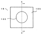
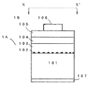
図4に本第6実施例に係るLED1Bの平面模式図を示す。また図5には、図4の破線X−X’に沿ったLED1Bの断面の構造を模式的に示す。図4及び図5において、上記の図1〜図3に示したのと同一の構成要素には、同一の符号を付して、その説明を省略する。
【0045】
本第6実施例に記載のLED1Bは、上記の第5実施例に記載の積層構造体1Aにオーミック電極を設けて構成した。n形のリン化硼素層105の表面の中央部には、同層105に接触する側に金・ゲルマニウム(Au・Ge)合金からなるオーミック電極を配置したAu・Ge/ニッケル(Ni)/Auの3層重層構造からなる表面電極106を設けた。結線用の台座(pad)電極を兼ねる表面電極106は、直径を約120μmとする円形の電極とした。また、p形Si単結晶基板101の裏面の略全面には、裏面電極107としてアルミニウム(Al)からなるオーミック電極を配置した。Al蒸着膜の膜厚は約2μmとした。これより、n形発光層104をp形及びn形リン化硼素層103、105で挟持したpn接合型DH構造のLED1Bを構成した。p形及びn形の双方のリン化硼素層103、104は何れも、室温での禁止帯幅として約3eVを有するため、発光層104に対するクラッド(clad)層として有効に利用できた。
【0046】
表面電極106と裏面電極107との間に順方向に20ミリアンペア(mA)の動作電流を通流したところ、LED1Bから波長を約440nmとする青紫帯光が発せられた。一般的な積分球を利用して測定されるチップ(chip)状態での輝度は9ミリカンデラ(mcd)となり、高発光強度のLED1Bが提供された。また、n形発光層104とp形リン化硼素層103との何れも表面の平坦性に優れる連続膜からpn接合が構成されているため、良好な整流特性が顕現され、順方向電圧(Vf、ただし順方向電流=20mA)は約3Vであり、逆方向電圧(VR、逆方向電流=10μA)は5V以上となった。
【0047】
【発明の効果】
結晶基板の表面上に、硼素とリンとを構成元素として含むリン化硼素系半導体層を気相成長させるリン化硼素系半導体層の製造方法に於いて、本発明に依れば、結晶基板の表面に硼素またはリンの何れかを含む粒子を予め、形成した後、次にリン化硼素系半導体層を気相成長させることとしたので、上記の粒子の「成長核」としての作用を利用して表面の平坦性に優れ、且つ連続性のあるリン化硼素系半導体層を気相成長させるに効果を挙げられる。
【0048】
また本発明に依れば、硼素またはリンの何れかを含む粒子を、特に多結晶から構成することとしたので、表面の平坦性に優れるリン化硼素系半導体層の連続膜を気相成長させるに効果を挙げられる。
【0049】
また本発明に依れば、硼素またはリンの何れかを含む粒子を結晶基板の表面との接合界面の領域に非晶質体を含む多結晶体から構成することとしたので、基板をなす結晶との格子ミスマッチを緩和する非晶質の作用に依り、表面の平坦性に優れ、且つ連続性のあるリン化硼素系半導体層を気相成長させるに特に効果が奏される。
【0050】
また本発明に依れば、リン化硼素系半導体層を、硼素またはリンの何れかを含む粒子を形成した温度を超えて、1200℃以下の基板温度で形成することとしたので、結晶性に優れるリン化硼素系半導体層を気相成長させるに効果を挙げられる。
【0051】
また本発明に依れば、リン化硼素系半導体層を、硼素またはリンの何れかを含む粒子を形成するに用いたと同一の硼素原料またはリン原料と同一の手段で気相成長させることとしたので、表面が平坦で連続性の優れるリン化硼素系半導体層を簡易に形成するに効果を挙げられる。
【0052】
また本発明に依れば、本発明の粒子の及ぼす作用に依りもたらされる表面の平坦性と連続性に優れるリン化硼素系半導体層を利用して半導体素子を構成することとしたので、例えば、良好な整流性を発揮するpn接合を構成でき、順方向及び逆方向電圧特性に優れる高発光強度のLEDを提供できる。
【図面の簡単な説明】
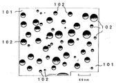
【図1】本発明の第1実施例に係る、基板表面に形成された硼素またはリンを含む粒子を示す原子間力顕微鏡像の模写図である。
【図2】 MOCVD装置の構成を示す概略図である。
【図3】 本発明の第4実施例に係る積層構造体の断面模式図である。
【図4】 本発明の第6実施例に記載のLEDの平面模式図である。
【図5】 図4に示すLEDの破線X−X’に沿った断面模式図である。
【図6】本発明の第3実施例に係るリン化硼素層の反射率の光の波長に対する依存性を示す図である。
【符号の説明】
1A 積層構造体
1B LED
11 MOCVD反応炉
12 導入孔
13 排出孔
14 基板支持台
15 高周波誘導コイル
16 硼素原料容器
17 リン原料容器
101 結晶基板
102 硼素またはリンを含む粒子
103 p形リン化硼素層
104 発光層
105 n形リン化硼素層
106 表面電極
107 裏面電極[0001]
BACKGROUND OF THE INVENTION
The present invention relates to a boron phosphide-based semiconductor layer and a semiconductor element using the boron phosphide-based semiconductor layer. In particular, the boron phosphide-based semiconductor layer having excellent surface flatness and continuity is vapor-phase grown on the surface of a crystal substrate. For technology.
[0002]
[Prior art]
Conventionally, boron phosphide-based semiconductor layers containing boron (B) and phosphorus (P) as constituent elements have been used to form various semiconductor elements. For example, a semiconductor layer made of boron phosphide (BP) which is a typical monomer as a boron phosphide-based semiconductor is used to form an n-type base layer of an npn heterobipolar transistor (HBT). (See J. Electrochem. Soc., 125 (4) (1978), pages 633-637). Further, in a blue laser diode (LD), it is used as a contact layer for forming an ohmic electrode having a low contact resistance (see Japanese Patent Laid-Open No. 10-242567). Further, it is used as a buffer layer for constituting a light emitting diode (LED) that emits light of a short wavelength such as near ultraviolet or blue (see US Pat. No. 6,069,021).
[0003]
The boron phosphide-based semiconductor layer for constituting the semiconductor element as described above has been conventionally formed by vapor phase growth means. Conventional vapor growth means include, for example, boron trichloride (BClThree) And phosphorus trichloride (PCl)Three) As a starting material (see “The Crystal Growth Society of Japan”, Vol. 24, No. 2 (1997), page 150), borane (BH)Three) Or diborane (B2H6) And phosphine (PHThree) And the like as raw materials (see J. Crystal Growth, 25/25 (1974), pages 193 to 196), molecular beam epitaxy (J. Solid State Chem., 133 (1997)) 269-272), and metal organic chemical vapor deposition (MOCVD) method (Inst. Phys. Conf. Ser., No. 129 (IOP Publishing Ltd. (UK, 1993), pp. 157-162)) Can be illustrated.
[0004]
In vapor phase growth of a boron phosphide-based semiconductor layer, a single crystal of a semiconductor material is exclusively used for the substrate. Conventionally, silicon (Si) single crystal (silicon) has been used as a practical substrate (see (1) J. Electrochem. Soc., 125 (1978) and (2) US Pat. No. 6,069,021). Silicon carbide (SiC) (see Japanese Patent Laid-Open No. 10-242568), gallium phosphide (GaP) (see Japanese Patent Laid-Open No. 10-242568), gallium nitride (GaN) (see Japanese Patent Laid-Open No. 10-247745), etc. The single crystal is used.
[0005]
[Problems to be solved by the invention]
However, the lattice constants of the single crystal material forming the substrate and, for example, boron phosphide (BP) are significantly different. The lattice constant of silicon single crystal is 5.431 Å, while that of cubic zinc blende BP is 4.538 ((Akira Teramoto, “Introduction to Semiconductor Devices” (March 30, 1995, ( The first edition issued by Baifukan Co., Ltd.), page 28). Therefore, the degree of lattice mismatch is as large as about 16.5% (Katsufusa Shono, “Semiconductor Technology (above)” (June 25, 1992, 9th edition, Tokyo University Press), 97- (See page 98).
[0006]
Thus, on a crystal substrate with a large degree of lattice mismatch, the boron phosphide-based semiconductor layer causes island-like growth in a growth mode similar to Volmer-Weber (Thin Film and Surface Physics Subcommittee of the Japan Society of Applied Physics) Ed., "Thin Film Handbook" (March 25, 1991, Kyoritsu Shuppan Co., Ltd., first edition, first edition), page 59). For this reason, it has been difficult to obtain a continuous boron phosphide-based semiconductor layer.
[0007]
If there is means for vapor-phase growth of a boron phosphide-based semiconductor layer having excellent continuity without cracks, the forward voltage (so-called Vf) is low due to, for example, the development of normal pn junction characteristics. LEDs and threshold voltages (so-called Vth) Can be easily provided. The present invention provides a vapor phase growth method for obtaining a boron phosphide-based semiconductor layer having excellent continuity even on a crystal substrate having a large degree of lattice mismatch. In addition, a semiconductor element configured using the boron phosphide-based semiconductor layer is provided.
[0008]
[Means for Solving the Problems]
That is, the present invention
(1) In a method for producing a boron phosphide-based semiconductor layer in which a boron phosphide-based semiconductor layer containing boron (B) and phosphorus (P) as constituent elements is vapor-phase grown on the surface of a crystal substrate, A boron phosphide-based semiconductor layer characterized in that particles containing either boron or phosphorus are formed in advance on the surface of the substrate, and then a boron phosphide-based semiconductor layer is vapor-phase grown on the surface of the crystal substrate. Production method.
(2) The method for producing a boron phosphide-based semiconductor layer according to (1) above, wherein the diameter of the particles containing either boron or phosphorus is 1 nm or more and 30 nm or less.
(3) The method for producing a boron phosphide-based semiconductor layer according to (1) or (2) above, wherein the crystal substrate is made of an n-type or p-type conductive single crystal.
(4) The production of a boron phosphide-based semiconductor layer according to any one of (1) to (3) above, wherein the particles containing either boron or phosphorus are formed of polycrystals. Method.
(5) The above-mentioned (1) to (1), wherein the particles containing either boron or phosphorus are formed from a polycrystalline material containing an amorphous material in a region of a bonding interface with the surface of the crystal substrate. 4. The method for producing a boron phosphide-based semiconductor layer according to any one of 4).
(6) The boron phosphide-based semiconductor layer is vapor-phase grown on the surface of the crystal substrate at a temperature that exceeds the temperature for forming particles containing either boron or phosphorus and is 1200 ° C. or lower. The method for producing a boron phosphide-based semiconductor layer according to any one of (1) to (5) above.
(7) The same vapor phase growth as that for forming particles containing either boron or phosphorus using the same raw material as the boron raw material or phosphorus raw material used to form particles containing either boron or phosphorus. The method for producing a boron phosphide-based semiconductor layer according to any one of (1) to (6) above, wherein the boron phosphide-based semiconductor layer is vapor-phase grown by means.
(8) The method for producing a boron phosphide-based semiconductor layer as described in (7) above, wherein the vapor phase growth means is a metal organic chemical vapor deposition (MOCVD) method.
(9) A boron phosphide-based semiconductor layer manufactured using the method for manufacturing a boron phosphide-based semiconductor layer described in any one of (1) to (8) above.
(10) A semiconductor device using the boron phosphide-based semiconductor layer according to (9).
It is.
[0009]
DETAILED DESCRIPTION OF THE INVENTION
In the present invention, a boron phosphide-based semiconductor includes boron and phosphorus as constituent elements, for example, BαAlβGaγIn1- α - β - γP1- δAsδ(0 <α ≦ 1, 0 ≦ β <1, 0 ≦ γ <1, 0 <α + β + γ ≦ 1, 0 ≦ δ <1), for example, BαAlβGaγIn1- α - β - γP1- δNδ(0 <α ≦ 1, 0 ≦ β <1, 0 ≦ γ <1, 0 <α + β + γ ≦ 1, 0 ≦ δ <1). To describe an example of the first embodiment of the present invention, first, for example, triethyl boron ((C2HFive)ThreeB) is uniformly adsorbed on the surface of the crystal substrate. In particular, boron-containing compounds that are liquid at room temperature, such as boron dioxide (B (OCHThree)ThreeIf melting point = −29 ° C., boiling point = + 68 to + 69 ° C.), etc., this is uniformly sprayed on the surface of the crystal substrate. Thereafter, the temperature of the crystal substrate is raised, the additional group is removed, and solidified as particles containing boron. The temperature of the crystal substrate is set to a temperature suitable for solidifying the boron-containing particles. In this way, before the continuous film of the boron phosphide-based semiconductor layer is vapor-phase grown, particles containing boron or phosphorus can be deposited on the surface of the substrate in advance.
[0010]
Particles containing phosphorus can be formed in the same manner. For example, a phosphine (PH) is formed on the surface of a crystal substrate placed inside an MOCVD growth furnace.Three) Is adsorbed. Thereafter, if the temperature of the crystal substrate is raised to a temperature of 400 ° C. or more and below the practical heat resistant temperature of the crystal substrate, the pH adsorbed on the surface of the crystal substrate is increased.ThreeThe molecules can be pyrolyzed to form particles containing phosphorus. For example, (C2HFive)ThreeB and PHThreeThere is also a means for causing particles containing both boron and phosphorus formed by vapor-phase reaction by simultaneously circulating them to fly toward the surface of the crystal substrate and adhere to the surface.
[0011]
The size of the particles containing boron or phosphorus provided on the crystal substrate is preferably 1 nm or more and 30 nm or less in terms of particle diameter (particle diameter). Particles whose particle diameter is extremely large exceeding 30 nm generally have a high elevation from the surface of the crystal substrate. In a boron phosphide-based semiconductor layer that grows on particles as “nuclei”, the presence of large particles results in a disadvantage that the flatness of the surface of the boron phosphide-based semiconductor layer is impaired. Further, in the case of fine particles having a particle diameter of less than 1 nm, the boron phosphide-based semiconductor layer grows only around the fine particles, which hinders obtaining a continuous film and becomes inconvenient.
[0012]
Furthermore, if the density of the particles present on the surface of the crystal substrate is low, a continuous boron phosphide-based semiconductor layer cannot be stably obtained. In order to stably obtain a continuous boron phosphide-based semiconductor layer, for example, particles having an average particle diameter of 10 nm are about 1 × 10 × 10.8/ Cm2It is desirable to exist on the surface of the crystal substrate at the above density. More desirably, the particles are present at a high density so as to almost completely cover the surface of the crystal substrate. More preferably, the surface of the crystal substrate is almost completely covered with particles that flatten the top plate. The particles that are substantially parallel to the surface of the crystal substrate and have a flat top plate contribute particularly to obtaining a boron phosphide-based semiconductor layer having a flat surface. As the total concentration of boron raw material or phosphorus raw material supplied to the surface of the crystal substrate is increased, particles having a larger particle diameter can be generated at higher density. The composition of the particles present on the surface of the crystal substrate can be investigated by, for example, a composition analysis method such as Auger electron analysis or electron microscope analysis. The particle diameter and particle density can be measured using, for example, an atomic force microscope (AFM).
[0013]
If particles containing either boron or phosphorus according to the present invention are formed on the surface of a crystal substrate, a continuous boron phosphide-based semiconductor layer can be formed on a single crystal substrate having a large degree of lattice mismatch. . For example, a group III-V compound semiconductor single crystal such as gallium arsenide (GaAs), a group III nitride semiconductor single crystal such as aluminum nitride (AlN), or a silicon (Si) single crystal can be used as the substrate. Insulating α-alumina (α-Al2OThree) A single crystal or a perovskite crystal type oxide single crystal can be used as a substrate. When an n-type or p-type conductive single crystal is used as a substrate, an ohmic electrode of positive or negative polarity of either polarity can be laid on the back surface of the substrate as a back electrode, contributing to the simple construction of light emitting elements such as LEDs. it can. A single crystal substrate having a low resistivity of 1 mΩ · cm or less contributes to an LED having a low forward voltage.
[0014]
The particles containing either boron or phosphorus according to the present invention may be composed of polycrystalline particles. Polycrystalline particles refer to crystal grains formed by, for example, single crystals having different orientations joined together via crystal grain boundaries. Polycrystalline particles may be composed of a collection of single crystals having different crystal types. For example, there is a polycrystalline particle composed of a single crystal having the same crystal type as the crystal forming the substrate and a single crystal having a different crystal type. Polycrystalline particles can be formed by setting the substrate temperature to be lower than the substrate temperature when the single crystal particles are formed. As an example of the second embodiment of the present invention, (C2HFive)ThreeIn a MOCVD growth furnace using B as a boron source (C2HFive)ThreeOn the surface of the silicon single crystal substrate held at a low temperature below the boiling point of B (= + 95 ° C.), (C2HFive)ThreeHydrogen associated with B (H2). After waiting for a while, the temperature of the silicon single crystal substrate is desirably raised to about 450 ° C. to about 650 ° C. Then, after waiting for a while, polycrystalline grains containing boron are formed on the surface of the crystal substrate. In this case, the longer the standby time at high temperature, the larger the polycrystalline grains can be obtained. In polycrystalline grains, lattice mismatch between the crystal substrate and the boron phosphide-based semiconductor layer is absorbed by crystal grain boundaries or stacking faults contained therein, and a high-quality boron phosphide-based semiconductor layer with few crystal defects can be obtained. It is effective to obtain. The constituents of the crystal grains can be analyzed by, for example, an electron diffraction technique using a transmission electron microscope (TEM).
[0015]
In the third embodiment of the present invention, in particular, after boron or phosphorus-containing particles are deposited on the surface of the crystal substrate, the temperature of the crystal substrate is suddenly increased, so that the junction boundary region with the crystal substrate is not formed. Form crystal grains. For example, (C2HFive)ThreeAfter forming boron-containing particles at 350 ° C. in a MOCVD growth furnace using B as a boron raw material, the particle is rapidly raised to 650 ° C. at a rate of 100 ° C. per minute to make the boundary region of the crystal substrate amorphous. To form crystal grains. The amorphous layer present in the region in the vicinity of the bonding interface with the crystal substrate relaxes the lattice mismatch with the crystal substrate, and can provide a boron phosphide-based semiconductor layer with excellent crystallinity with less distortion. According to an electron diffraction technique using a transmission electron microscope (TEM), it is possible to identify the presence or absence of an amorphous material in a region near a bonding interface with a crystal substrate.
[0016]
Particles containing boron or phosphorus formed in advance on the surface of the crystal substrate act as growth nuclei, and are effective in providing a continuous boron phosphide-based semiconductor layer. In order to grow a boron phosphide-based semiconductor layer using these particles as nuclei, the temperature of the crystal substrate when growing the boron phosphide-based semiconductor layer exceeds the temperature at which particles containing either boron or phosphorus are formed, It is suitable that the temperature is 1200 ° C. or lower. Growing a boron phosphide-based semiconductor layer at the same temperature at which the particles are formed is disadvantageous in many cases because it results in a polycrystalline boron phosphide-based semiconductor layer with irregular alignment. A preferable temperature is a temperature of 750 ° C. or higher and 1200 ° C. or lower. High temperature exceeding 1200 ° C is, for example, B6P or B13P2Such a boron phosphide multimer is generated, which is inconvenient for obtaining a compositionally uniform boron phosphide-based semiconductor layer. As an example of the fourth embodiment of the present invention, particles containing boron and phosphorus are formed in advance on the surface of a p-type silicon single crystal at 450 ° C. and then increased to 1050 ° C. at a rate of 75 ° C. per minute. And a method of forming a continuous film of monomeric boron phosphide (BP) by MOCVD.
[0017]
Means for forming a boron phosphide-based semiconductor layer using boron or phosphorus-containing grains as growth nuclei include pre-brown halogen vapor phase epitaxy, hydride vapor phase epitaxy, molecular beam epitaxy, and There are vapor phase growth means such as metal organic chemical vapor deposition (MOCVD). If the particles provided on the surface of the crystal substrate and the boron phosphide-based semiconductor layer on the particles are formed by the same vapor phase growth means using the same boron raw material or phosphorus raw material, it is advantageous for simple configuration. It becomes. In particular, in MOCVD means, particles caused by halogen species in halogen vapor phase growth means using chloride or bromide as a raw material (see J. Appl. Phys., 42 (1) (1971), pages 420 to 424). There is an advantage that etching (etching) can be avoided. This is a convenient way to form a boron phosphide-based semiconductor layer without reducing the density of particles formed on the crystal substrate surface. As an example of the fifth embodiment of the present invention, a particle containing boron or phosphorus and a boron phosphide-based semiconductor layer are formed as (C2HFive)ThreeA means for forming B by the MOCVD method using the same boron raw material can be mentioned. PHThreeIs a means for forming particles and a boron phosphide-based semiconductor layer by atmospheric pressure (substantially atmospheric pressure) or reduced pressure MOCVD.
[0018]
Various semiconductor elements can be formed by forming a boron phosphide-based semiconductor layer provided with grains containing boron or phosphorus as growth nuclei. For example, an n-type boron phosphide-based semiconductor layer formed through particles containing boron and phosphorus formed on an n-type silicon carbide (SiC) single crystal substrate can be used as a barrier (cladding) layer in an LED. Insulating sapphire (α-Al2OThreeSingle-crystal) An oxygen-doped high-resistance boron phosphide-based semiconductor layer formed through particles containing boron and phosphorus formed on the substrate surface can be used as a high-resistance buffer layer for field effect transistor (FET) applications. Various specifications such as layer thickness and resistance of the boron phosphide-based semiconductor layer provided via boron or phosphorus-containing particles are determined in view of the function to be performed by the layer. For example, from a monomeric boron phosphide layer having a forbidden band width of about 3 eV at room temperature, a clad layer that also serves as a light-emitting reflective layer capable of reflecting light of a specific wavelength with high reflectivity by adjusting the layer thickness (See Japanese Patent Application No. 2002-18188).
[0019]
[Action]
When the boron phosphide-based semiconductor layer is vapor-phase grown on the surface of the crystal substrate, particles containing either boron or phosphorus previously formed on the surface of the crystal substrate cause the subsequent growth of the boron phosphide-based semiconductor layer. Act as a growth nucleus to promote.
[0020]
In particular, a polycrystalline particle containing boron or phosphorus has an effect of providing a boron phosphide-based semiconductor layer having few crystal defects and excellent crystallinity regardless of the presence of a lattice mismatch between the crystal substrate and the boron phosphide-based semiconductor layer. Have
[0021]
In particular, when a particle containing boron or phosphorus is formed from a polycrystalline body containing an amorphous material in a region of a bonding interface with the surface of the crystalline substrate, the amorphous material is formed from the crystalline substrate and the boron phosphide-based semiconductor layer. It exerts the effect of relaxing the lattice mismatch with and providing a boron phosphide-based semiconductor layer with excellent crystallinity.
[0022]
【Example】
(First embodiment)
The present invention will be specifically described by taking as an example the case where a boron phosphide semiconductor layer is vapor-phase grown after previously forming particles containing either boron or phosphorus on a crystal substrate.
[0023]
In the first embodiment, a general halogen vapor phase growth apparatus (for example, Electronic Communication Society “Semiconductor / Transistor Research Group / Material No. SSD74-89 (1975-03)” (March 25, 1975) The particles containing boron and phosphorus were formed on the surface of a Si single crystal substrate having a p-type {111} plane by using a boron-
[0024]
FIG. 1 is a copy of an atomic force microscope image of the
[0025]
After forming the
[0026]
First, after placing the Si
[0027]
(Second embodiment)
In the second embodiment, the present invention will be described by taking as an example the case where polycrystalline grains are previously formed on a crystal substrate by halogen vapor phase epitaxy and then the boron phosphide semiconductor layer is vapor phase grown by MOCVD. The contents of will be specifically described.
[0028]
Different from the first embodiment, the temperature-related conditions were different, and boron or phosphorus-containing particles were formed on a Si single crystal substrate by halogen vapor phase epitaxy. In the second embodiment, a BCl gas and a hydrogen carrier gas are used under the same conditions as in the first embodiment toward the surface of the Si single crystal substrate maintained at about 23 ° C. at room temperature.ThreeAnd PClThreeAnd droplets of boron raw material and phosphorus raw material were deposited on the surface of the substrate. Thereafter, the supply of the raw material into the halogen vapor phase growth apparatus was stopped, and the temperature of the substrate was increased to 650 ° C. at a rate of temperature increase of 20 ° C. per minute to solidify the droplets. Analysis by a general cross-sectional TEM technique revealed that the particles solidified under these conditions were polycrystalline containing flat, generally spherical boron and / or phosphorus having a diameter of approximately 5 nm, or both. . Further, in the measurement using an atomic force microscope, the particles were distributed almost uniformly on the surface of the substrate having a diameter of 2 inches with an average distance of about 10 nm.
[0029]
However, in the Auger electron analysis, fine precipitates with a diameter of several tens of nanometers mainly consisting of phosphorus oxide were confirmed on the surface. The in-plane density of the precipitate is about 100 / cm.2It was about. In the vapor phase growth according to the second embodiment, as in the case of the first embodiment, boron or phosphorus-containing particles and the boron phosphide layer are formed by different vapor phase growth means. Therefore, after forming the grains, it was necessary to take out the silicon single crystal substrate from the apparatus and place it again in the MOCVD reactor in which the boron phosphide layer is vapor-grown. Therefore, the silicon single crystal substrate on which the particles are formed is exposed to the atmosphere, and at this time, it is thought that precipitates are formed by oxidizing the particles containing boron or phosphorus.
[0030]
Next, in accordance with the same means as in the first embodiment, a boron phosphide semiconductor layer was formed by atmospheric pressure MOCVD using the polycrystalline particles as growth nuclei. The obtained boron phosphide semiconductor layer was a continuous film with no visible cracks.
[0031]
(Third embodiment)
In the third embodiment, an example in which the boron phosphide semiconductor layer is vapor-phase grown after previously forming particles containing amorphous in the region of the bonding interface with the crystal substrate on the crystal substrate will be described. The contents of the invention will be specifically described.
[0032]
A boron raw material and a phosphorus raw material were deposited on the surface of the silicon single crystal substrate at 450 ° C. by the same means as in the first example. Thereafter, the substrate temperature was rapidly increased to 1050 ° C. at a heating rate of 150 ° C. per minute. By this temperature raising operation, particles containing boron or phosphorus, in which the region of the bonding interface with the silicon single crystal substrate was made amorphous, were formed. Thereafter, the monomeric boron phosphide semiconductor layer was vapor-phase grown by the same means as in the first example.
[0033]
FIG. 6 shows the dependence of the reflectance of the boron phosphide semiconductor layer vapor-grown on the silicon single crystal substrate of the third embodiment with respect to the wavelength of light. The reflectance of blue band light having a wavelength of about 450 nm is about 30% and about 33% in the case of the boron phosphide semiconductor layer fabricated in the first and second embodiments, respectively. In the three examples, the highest was about 43%. From this, it was shown that the particles containing amorphous are effective in providing a boron phosphide layer having particularly excellent surface flatness.
[0034]
(Fourth embodiment)
In the fourth embodiment, the content of the present invention will be described more specifically by taking as an example a case where a boron phosphide semiconductor layer is vapor-phase grown after previously forming amorphous particles on a crystal substrate. .
[0035]
FIG. 3 schematically shows a cross-sectional structure of an epitaxial multilayer structure 1A according to the fourth embodiment. In addition, about the same component as shown in FIG.1 and FIG.2, the same code | symbol is attached | subjected and the description is abbreviate | omitted.
[0036]
In the fourth embodiment, the layer thickness is approximately 240 nm, and the carrier (hole) concentration is approximately 2 × 10, which is manufactured by the same method as in the third embodiment.19cm-3On the p-type boron phosphide layer 103, trimethylgallium ((CHThree)ThreeGa) / Ammonia (NHThree) / Hydrogen (H2) N-type Ga using normal atmospheric pressure MOCVD0.90In0.10The N layer was stacked as the light emitting layer 104. The layer thickness of the light emitting layer 104 is set to about 65 nm, and the carrier (electron) concentration is about 4 × 10.18cm-3Set to. Wurtzite crystal type Ga forming the light emitting layer 1040.90In0.10The a-axis lattice constant of the N layer is about 3.216Å, and the {110} crystal plane lattice plane of the zinc phosphite crystal-type monomer boron phosphide (lattice constant ≒ 4.538Å) as the underlayer It was decided to coincide with the interval (≈3.209 mm).
[0037]
On the light emitting layer 104, (C2HFive)ThreeB / PHThree/ H2An n-type monomeric boron phosphide (BP)
[0038]
In the fourth embodiment, in particular, the p-type boron phosphide layer 103 was vapor-phase grown using amorphous particles as growth nuclei, so that it became a continuous film and had excellent surface flatness. For this reason, both the light emitting layer 104 and the n-type
[0039]
(5th Example)
In the fifth embodiment, the contents of the present invention are described by taking as an example the case where both the particles on the crystal substrate surface and the boron phosphide semiconductor layer are formed by MOCVD using the same boron source and phosphorus source. This will be specifically described.
[0040]
In the fifth embodiment, using the MOCVD apparatus shown in FIG. 2, particles containing boron or phosphorus containing amorphous are formed on a p-type silicon single crystal substrate having a (111) plane. Boron raw materials include (C2HFive)ThreeB was used. The phosphorus raw material is PHThreeIt was. (C2HFive)ThreeB was supplied into the
[0041]
After stopping the supply of the boron raw material into the
[0042]
The surfaces of the p-type boron phosphide layer, the light emitting layer, and the n-type boron phosphide layer grown by vapor phase through the
[0043]
(Sixth embodiment)
In the sixth embodiment, an example in which an LED is formed using a boron phosphide-based semiconductor layer obtained by vapor-phase growth using amorphous particles on a crystal substrate as growth nuclei will be described. Will be described in detail.
[0044]
FIG. 4 shows a schematic plan view of an LED 1B according to the sixth embodiment. FIG. 5 schematically shows a cross-sectional structure of the LED 1B along the broken line X-X ′ in FIG. 4 and 5, the same components as those shown in FIGS. 1 to 3 are given the same reference numerals, and descriptions thereof are omitted.
[0045]
The LED 1B described in the sixth example is configured by providing an ohmic electrode on the laminated structure 1A described in the fifth example. At the center of the surface of the n-type
[0046]
When an operating current of 20 milliamperes (mA) was passed between the front electrode 106 and the back electrode 107 in the forward direction, blue-violet light having a wavelength of about 440 nm was emitted from the LED 1B. The luminance in a chip state measured using a general integrating sphere was 9 millicandela (mcd), and an LED 1B having high emission intensity was provided. In addition, since both the n-type light emitting layer 104 and the p-type boron phosphide layer 103 are formed of a pn junction from a continuous film having excellent surface flatness, good rectification characteristics are manifested, and the forward voltage (Vf However, the forward current = 20 mA) was about 3 V, and the reverse voltage (VR, reverse current = 10 μA) was 5 V or more.
[0047]
【The invention's effect】
According to the present invention, there is provided a method for producing a boron phosphide-based semiconductor layer in which a boron phosphide-based semiconductor layer containing boron and phosphorus as constituent elements is vapor-phase grown on a surface of a crystal substrate. Since particles containing either boron or phosphorus on the surface were previously formed, and then the boron phosphide-based semiconductor layer was vapor-phase grown, the above-mentioned action as a “growth nucleus” was utilized. This is effective for vapor phase growth of a boron phosphide-based semiconductor layer having excellent surface flatness and continuity.
[0048]
In addition, according to the present invention, since the particles containing either boron or phosphorus are made of polycrystalline in particular, a continuous film of a boron phosphide-based semiconductor layer having excellent surface flatness is vapor-phase grown. Can be effective.
[0049]
Further, according to the present invention, since the particles containing either boron or phosphorus are composed of a polycrystalline body containing an amorphous body in the region of the bonding interface with the surface of the crystalline substrate, the crystal forming the substrate Is particularly effective for vapor phase growth of a boron phosphide-based semiconductor layer having excellent surface flatness and continuity.
[0050]
Further, according to the present invention, the boron phosphide-based semiconductor layer is formed at a substrate temperature of 1200 ° C. or lower, exceeding the temperature at which particles containing either boron or phosphorus are formed. This is effective for vapor phase growth of an excellent boron phosphide-based semiconductor layer.
[0051]
Further, according to the present invention, the boron phosphide-based semiconductor layer is vapor-phase grown by the same means as the boron raw material or the phosphorus raw material used to form the particles containing either boron or phosphorus. Therefore, it is effective to easily form a boron phosphide-based semiconductor layer having a flat surface and excellent continuity.
[0052]
Further, according to the present invention, since the semiconductor element is configured using the boron phosphide-based semiconductor layer having excellent surface flatness and continuity brought about by the action of the particles of the present invention, for example, A pn junction that exhibits good rectification can be configured, and an LED with high emission intensity that is excellent in forward and reverse voltage characteristics can be provided.
[Brief description of the drawings]
FIG. 1 is a copy of an atomic force microscope image showing particles containing boron or phosphorus formed on a substrate surface according to a first embodiment of the present invention.
FIG. 2 is a schematic view showing the configuration of an MOCVD apparatus.
FIG. 3 is a schematic cross-sectional view of a multilayer structure according to a fourth embodiment of the present invention.
FIG. 4 is a schematic plan view of an LED according to a sixth embodiment of the present invention.
5 is a schematic sectional view taken along a broken line X-X ′ of the LED shown in FIG. 4;
FIG. 6 is a graph showing the dependency of the reflectance of the boron phosphide layer according to the third embodiment of the present invention on the wavelength of light.
[Explanation of symbols]
1A Laminated structure
1B LED
11 MOCVD reactor
12 Introduction hole
13 Discharge hole
14 Substrate support stand
15 High frequency induction coil
16 Boron material container
17 Phosphorus raw material container
101 Crystal substrate
102 Particles containing boron or phosphorus
103 p-type boron phosphide layer
104 Light emitting layer
105 n-type boron phosphide layer
106 Surface electrode
107 Back electrode
Claims (11)
Priority Applications (1)
| Application Number | Priority Date | Filing Date | Title |
|---|---|---|---|
| JP2002079865A JP3700664B2 (en) | 2002-03-22 | 2002-03-22 | Boron phosphide-based semiconductor layer, manufacturing method thereof, and semiconductor element |
Applications Claiming Priority (1)
| Application Number | Priority Date | Filing Date | Title |
|---|---|---|---|
| JP2002079865A JP3700664B2 (en) | 2002-03-22 | 2002-03-22 | Boron phosphide-based semiconductor layer, manufacturing method thereof, and semiconductor element |
Publications (3)
| Publication Number | Publication Date |
|---|---|
| JP2003282450A JP2003282450A (en) | 2003-10-03 |
| JP2003282450A5 JP2003282450A5 (en) | 2005-05-19 |
| JP3700664B2 true JP3700664B2 (en) | 2005-09-28 |
Family
ID=29229130
Family Applications (1)
| Application Number | Title | Priority Date | Filing Date |
|---|---|---|---|
| JP2002079865A Expired - Fee Related JP3700664B2 (en) | 2002-03-22 | 2002-03-22 | Boron phosphide-based semiconductor layer, manufacturing method thereof, and semiconductor element |
Country Status (1)
| Country | Link |
|---|---|
| JP (1) | JP3700664B2 (en) |
Families Citing this family (4)
| Publication number | Priority date | Publication date | Assignee | Title |
|---|---|---|---|---|
| GB2438567B (en) * | 2005-03-22 | 2010-06-23 | Sumitomo Chemical Co | Free-standing substrate, method for producing the same and semiconductor light-emitting device |
| JP2006352079A (en) * | 2005-03-22 | 2006-12-28 | Sumitomo Chemical Co Ltd | Self-supporting substrate, manufacturing method thereof and semiconductor light-emitting element |
| KR101053111B1 (en) * | 2011-02-28 | 2011-08-01 | 박건 | Nitride based light emitting device using silicon substrate and method of manufacturing the same |
| JP6008661B2 (en) * | 2012-08-29 | 2016-10-19 | 日東光器株式会社 | GaN crystal and method for manufacturing semiconductor device |
-
2002
- 2002-03-22 JP JP2002079865A patent/JP3700664B2/en not_active Expired - Fee Related
Also Published As
| Publication number | Publication date |
|---|---|
| JP2003282450A (en) | 2003-10-03 |
Similar Documents
| Publication | Publication Date | Title |
|---|---|---|
| US6787814B2 (en) | Group-III nitride semiconductor light-emitting device and production method thereof | |
| US7674644B2 (en) | Method for fabrication of group III nitride semiconductor | |
| US7772599B2 (en) | Gallium nitride-based semiconductor stacked structure, production method thereof, and compound semiconductor and light-emitting device each using the stacked structure | |
| JP2006173590A (en) | Gallium nitride-based semiconductor laminated structure, manufacturing method thereof, gallium nitride-based semiconductor element, and lamp | |
| TWI250663B (en) | Group-III nitride semiconductor device, production method thereof and light-emitting diode | |
| JP3772816B2 (en) | Gallium nitride crystal substrate, method for manufacturing the same, gallium nitride semiconductor device, and light emitting diode | |
| JP3700664B2 (en) | Boron phosphide-based semiconductor layer, manufacturing method thereof, and semiconductor element | |
| JP2002084001A (en) | Group iii nitride semiconductor light emitting diode, light emitting diode lamp, light source, electrode for group iii nitride semiconductor light emitting diode and its manufacturing method | |
| JP2004115305A (en) | Gallium nitride single crystal substrate, method of manufacturing the same, gallium nitride-based semiconductor device and light emitting diode | |
| JP4313478B2 (en) | AlGaInP light emitting diode | |
| JP3695416B2 (en) | Boron phosphide-based semiconductor layer, manufacturing method thereof, and boron phosphide-based semiconductor element | |
| JP4439400B2 (en) | Boron phosphide-based semiconductor light emitting device, manufacturing method thereof, and light emitting diode | |
| JP2001015803A (en) | AlGaInP LIGHT EMITTING DIODE | |
| JP3931740B2 (en) | Boron phosphide-based semiconductor device, manufacturing method thereof, and LED | |
| JP4158437B2 (en) | Method for producing p-type boron phosphide semiconductor layer, boron phosphide-based semiconductor element, and LED | |
| JP3592616B2 (en) | Group III nitride semiconductor light emitting device | |
| KR100981077B1 (en) | Compound semiconductor device | |
| JP4174910B2 (en) | Group III nitride semiconductor device | |
| JP2006024903A (en) | Gallium nitride based semiconductor multilayer structure | |
| JP3895266B2 (en) | BORON PHOSPHIDE COMPOUND SEMICONDUCTOR DEVICE, ITS MANUFACTURING METHOD, AND LIGHT EMITTING DIODE | |
| JP3928536B2 (en) | Method for manufacturing boron phosphide single crystal substrate | |
| JP3711966B2 (en) | Vapor phase growth method of group III nitride semiconductor layer and group III nitride semiconductor device | |
| JP2002289973A (en) | Iii nitride semiconductor light emitting element | |
| JP2001007395A (en) | Iii nitride semiconductor light emitting element | |
| JP3731567B2 (en) | Vapor phase growth method of boron phosphide layer, boron phosphide-based semiconductor device and LED |
Legal Events
| Date | Code | Title | Description |
|---|---|---|---|
| A521 | Written amendment |
Free format text: JAPANESE INTERMEDIATE CODE: A523 Effective date: 20040708 |
|
| A621 | Written request for application examination |
Free format text: JAPANESE INTERMEDIATE CODE: A621 Effective date: 20040708 |
|
| A977 | Report on retrieval |
Free format text: JAPANESE INTERMEDIATE CODE: A971007 Effective date: 20050614 |
|
| TRDD | Decision of grant or rejection written | ||
| A01 | Written decision to grant a patent or to grant a registration (utility model) |
Free format text: JAPANESE INTERMEDIATE CODE: A01 Effective date: 20050621 |
|
| A61 | First payment of annual fees (during grant procedure) |
Free format text: JAPANESE INTERMEDIATE CODE: A61 Effective date: 20050704 |
|
| R150 | Certificate of patent or registration of utility model |
Free format text: JAPANESE INTERMEDIATE CODE: R150 |
|
| FPAY | Renewal fee payment (event date is renewal date of database) |
Free format text: PAYMENT UNTIL: 20090722 Year of fee payment: 4 |
|
| FPAY | Renewal fee payment (event date is renewal date of database) |
Free format text: PAYMENT UNTIL: 20090722 Year of fee payment: 4 |
|
| FPAY | Renewal fee payment (event date is renewal date of database) |
Free format text: PAYMENT UNTIL: 20110722 Year of fee payment: 6 |
|
| FPAY | Renewal fee payment (event date is renewal date of database) |
Free format text: PAYMENT UNTIL: 20110722 Year of fee payment: 6 |
|
| FPAY | Renewal fee payment (event date is renewal date of database) |
Free format text: PAYMENT UNTIL: 20140722 Year of fee payment: 9 |
|
| LAPS | Cancellation because of no payment of annual fees |