JP3689183B2 - Accurate and effective sticky bit calculation for accurate floating-point division / square root operations - Google Patents
Accurate and effective sticky bit calculation for accurate floating-point division / square root operations Download PDFInfo
- Publication number
- JP3689183B2 JP3689183B2 JP16750896A JP16750896A JP3689183B2 JP 3689183 B2 JP3689183 B2 JP 3689183B2 JP 16750896 A JP16750896 A JP 16750896A JP 16750896 A JP16750896 A JP 16750896A JP 3689183 B2 JP3689183 B2 JP 3689183B2
- Authority
- JP
- Japan
- Prior art keywords
- bit
- carry
- sum
- zero
- partial remainder
- Prior art date
- Legal status (The legal status is an assumption and is not a legal conclusion. Google has not performed a legal analysis and makes no representation as to the accuracy of the status listed.)
- Expired - Fee Related
Links
Images
Classifications
-
- G—PHYSICS
- G06—COMPUTING; CALCULATING OR COUNTING
- G06F—ELECTRIC DIGITAL DATA PROCESSING
- G06F7/00—Methods or arrangements for processing data by operating upon the order or content of the data handled
- G06F7/38—Methods or arrangements for performing computations using exclusively denominational number representation, e.g. using binary, ternary, decimal representation
- G06F7/48—Methods or arrangements for performing computations using exclusively denominational number representation, e.g. using binary, ternary, decimal representation using non-contact-making devices, e.g. tube, solid state device; using unspecified devices
- G06F7/52—Multiplying; Dividing
- G06F7/535—Dividing only
-
- G—PHYSICS
- G06—COMPUTING; CALCULATING OR COUNTING
- G06F—ELECTRIC DIGITAL DATA PROCESSING
- G06F7/00—Methods or arrangements for processing data by operating upon the order or content of the data handled
- G06F7/38—Methods or arrangements for performing computations using exclusively denominational number representation, e.g. using binary, ternary, decimal representation
- G06F7/48—Methods or arrangements for performing computations using exclusively denominational number representation, e.g. using binary, ternary, decimal representation using non-contact-making devices, e.g. tube, solid state device; using unspecified devices
- G06F7/544—Methods or arrangements for performing computations using exclusively denominational number representation, e.g. using binary, ternary, decimal representation using non-contact-making devices, e.g. tube, solid state device; using unspecified devices for evaluating functions by calculation
- G06F7/552—Powers or roots, e.g. Pythagorean sums
- G06F7/5525—Roots or inverse roots of single operands
-
- G—PHYSICS
- G06—COMPUTING; CALCULATING OR COUNTING
- G06F—ELECTRIC DIGITAL DATA PROCESSING
- G06F7/00—Methods or arrangements for processing data by operating upon the order or content of the data handled
- G06F7/38—Methods or arrangements for performing computations using exclusively denominational number representation, e.g. using binary, ternary, decimal representation
- G06F7/48—Methods or arrangements for performing computations using exclusively denominational number representation, e.g. using binary, ternary, decimal representation using non-contact-making devices, e.g. tube, solid state device; using unspecified devices
- G06F7/483—Computations with numbers represented by a non-linear combination of denominational numbers, e.g. rational numbers, logarithmic number system or floating-point numbers
- G06F7/487—Multiplying; Dividing
- G06F7/4873—Dividing
-
- G—PHYSICS
- G06—COMPUTING; CALCULATING OR COUNTING
- G06F—ELECTRIC DIGITAL DATA PROCESSING
- G06F7/00—Methods or arrangements for processing data by operating upon the order or content of the data handled
- G06F7/38—Methods or arrangements for performing computations using exclusively denominational number representation, e.g. using binary, ternary, decimal representation
- G06F7/48—Methods or arrangements for performing computations using exclusively denominational number representation, e.g. using binary, ternary, decimal representation using non-contact-making devices, e.g. tube, solid state device; using unspecified devices
- G06F7/499—Denomination or exception handling, e.g. rounding or overflow
- G06F7/49942—Significance control
- G06F7/49947—Rounding
- G06F7/49952—Sticky bit
Description
【0001】
【発明の属する技術分野】
本発明はマイクロプロセッサ内の浮動小数点除算器(Floating point dividers)の分野、より詳細には、SRT除算/平方根演算のインプリメンテーション(SRT division/square root implementation)における商デジット選択規則(Quotient digit selection rules)に関し、同規則は結果が正確な場合、負の最終部分剰余(Negative final partial remainders)の形成を防止する。
【0002】
【従来の技術及び発明が解決しようとする課題】
SRTアルゴリズムは引き放し法除算(Non-restoring division)を実行する1つの方法を提供する。この詳細については、1958年9月に発行された米国電気電子学会コンピュータ部会会報(IEEE Trans. Comput.)第C−7巻218〜222頁に記載されているジェイ.イー.ロバートソンによる“デジタル除算法の新たなクラス”と、1958年に発行されたメカニカル応用数学誌(Quart. J. Mech. Appl. Math.)第11刊第3部364〜384頁に記載されているケー.ディー.トーチャーによる“自動2進コンピュータのための乗算及び除算技術”を参照のこと。デジタル除算では、オペランドとして除数及び被除数が使用され、かつ出力として商が形成される。複数の商デジットは反復計算され、同商デジットのうちの最上位商デジットが最初に形成される。SRT除算は他の除算アルゴリズムとは異なる。SRT除算では、連続する各商デジットは上位の僅かな部分剰余デジットのみに基づいて公式化され、非常に多くのデジットを含み得る部分剰余全体に基づいて公式化されることはない。全ての反復において、正確な商デジットの選択は部分剰余全体を考慮せずには保証できない。このため、SRTアルゴリズムは不正確な商デジットを時々形成する。しかし、SRTアルゴリズムは正、ゼロ及び負の各商デジットの可能性を提供する。商デジットを1つの反復において過大予測した場合、誤りは負の商デジットを選択することにより、次の反復において補正される。SRT除算では、商デジットを過小予測してはならない。即ち、商デジットは常に過大予測するか、または正確に予測する必要がある。全ての商デジットを過小予測しなかった場合、部分剰余は所定の上下限内に維持され、正確な最終商の計算が可能になる。SRTアルゴリズムは負の商デジットの形成を可能にする。このため、一般的に最終商出力は通常の除算のように全商デジットを単に連結するのではなく、寧ろ商デジットの重み付け加算及び減算を介して行われる。
【0003】
基数が更に大きい場合、1つの反復において形成される商デジットの数が更に多くなる。これは複雑さを増大させる。基数2のインプリメンテーションは1つのデジットを1つの反復において形成する。基数4のインプリメンテーションは2つのデジットを1つの反復において形成する。図1はSRTに基づく基数2を使用する簡単な浮動小数点インプリメンテーション(Simple SRT radix-2 floating point implementation)を示す。同インプリメンテーションは、除数及び被除数の両方が正であって、かつ正規化されていることを要する。従って、1/2≦D、被除数<1となる。シフトされた最初の部分剰余(Initial shifted partial remainder)、即ち2PR[0]は被除数である。第1商デジットの計算の反復(First quotient digit calculation iteration)開始前に、被除数は部分剰余レジスタ100に対してロードされる。この結果、最初の部分剰余は被除数となる。その後、反復によって形成される部分剰余は以下の数式1に基づいて形成される。
【0004】
【数1】

【0005】
部分剰余は一般的に冗長桁上げ保留の形態に維持される。この結果、次の部分剰余の計算では、更に処理速度が遅く、かつ大きい桁上げ伝搬加算器に代えて桁上げ保留加算器の使用が可能である。部分剰余は全ての反復が実施され、かつ所望の精度に達した後で、非冗長形態(Non-redundant form)へ変換される。SRTアルゴリズムは商デジットの過大予測を可能にする。商デジットの過大予測により、負の部分剰余が続いて形成される。このため、最終部分剰余を負にすべく最後の商デジットを過大予測し得る。この場合、過大予測に対する補正が不可能なため、Q及びQ−1の維持が必要である。この結果、最終部分剰余が負である場合、Q−1がQに代えて選択される。商デジットは常には冗長形態に維持され、さらには最後の反復において非冗長形態へ変換される。これに代えて、商(即ちQ)と、商−1(即ちQ−1)とを1992年12月に発行された米国電気電子学会コンピュータ部会会報(IEEE Trans. Comput.)第41巻第12号の1497〜1503頁に記載されているエム.ディ.エルセゴバック及びティ.ラングによる“オン・ザ・フライ・ラウンディング(On-the-fly rounding)”に開示されている規則に基づいてフライ(Fly)上に形成し得る。
【0006】
SRTアルゴリズムは平方根演算にも適用される。これにより、従来の除算ハードウェアの使用が可能である。簡略化された平方根の式は除算の式に類似している。これについては、1990年8月に発行された米国電気電子学会コンピュータ部会会報(IEEE Trans. Comput.)の第39巻第8号の1016〜1024頁に記載されているエム.ディ.エルセゴバック及びティ.ラングによる“初期PLAを伴わない基数4を使用した平方根演算(Radix-4 square root without initial PLA)”を参照のこと。平方根演算の反復方程式を以下の数式2に示す。
【0007】
【数2】
【0008】
2進法の除算アルゴリズムはグラマー・スクールで教授されている標準的な十進法の除算に類似している。R/D=Qにおいて、Qに対する各商デジットが予測される。第1商デジットを決定すべく、商デジットの適切な予測値に対して除数が掛けられる。次いで、その積は剰余を形成すべく被除数から引かれる。剰余が除数より更に大きい場合、商デジットの予測値は過小である。更に、剰余が負である場合、商デジットの予測値は過大である。いづれにしても、商デジットの予測値が誤っている場合、予測値の変更が必要である。この結果、正確な商デジットは次のデジットへ進む前に導き出される。次の関係、即ち0≦PR<Dが正しい場合、商デジットは正しい。ここで、PRは除数を掛けた商デジットを引いた後の部分剰余を示す。
【0009】
SRT除算アルゴリズムの鍵としては、負の商デジットを使用し得る点が挙げられる。例えば、基数10において、商デジットは標準デジット0〜9に加えて、−1〜−9の値を有し得る。600÷40の除算演算を以下に例示する。各反復において、正しい商デジットを選択した場合、正しい結果は15になる。しかし、正しいデジットである1に代えて、商デジットとして2が第1の反復中に選択されたと仮定する。第1の商デジットとして2を選択した後の部分剰余は600−(2*40*101)=−200である。SRT除算では、このエラーを補正すべくバックアップを行い、かつ第1の反復を繰り返すことはない。寧ろ、エラーは次の反復において補正可能である。SRT除算に基づき、第2の商デジットとして−5を正しく予測したと仮定する。反復後、部分剰余は−200−(−5*40*100)=0となる。反復後の部分剰余がゼロの場合、残りの全てのデジットの正しい値はゼロになる。従って、計算結果は(2*101)+(−5*100)=15となり、同計算結果は正しい。従って、SRTアルゴリズムは、後から1つ以上の負の商デジットを選択することにより、任意の商デジットの過大予測の補正を可能にする。その後の部分剰余を実質的にゼロまで削減すべく、予測された商デジットから正しい商デジットを引いた値が1を上回ってはならない。商デジットの予測における誤りが+1を上回ることを許容した場合、−9を下回る商デジット(例:−10、−11等)が底10において必要とされる。同様に、商デジットの範囲はSRTアルゴリズムに基づいて正の方向へ拡大されることはない。このため、正しい商デジットの過小予測は致命的である。これは部分剰余が基数を掛けた除数より更に大きく、かつその後、底10において9を上回る商デジット(例:10、11等)を必要とすることに起因する。従って、部分剰余を所定の上下限内に維持するために、商デジット選択において、正しい商デジットを過小予測してはならない。更に、商デジット選択において商デジットが過大予測された場合、予測された商デジットから正しい商デジットを引いた値は1を上回ってはならない。
【0010】
部分剰余を所定の上下限内に維持するための前記の基準を全ての部分剰余デジットを使用することなく満足させ得る点が保証される。正しい演算結果の算出を可能にする商デジットを選択するためには、部分剰余のうちの上位の僅かなデジットのみを使用すればよい。
【0011】
SRT除算は冗長商表示を負以外のデジットのみを有する標準的な非冗長形態まで削減するために、全ての商デジットの選択後に最終加算を要する。
最近の電子計算回路に用いられる2進法(底2)では、SRT除算は+1、0または−1の商デジットを提供する。商選択デジットを形成するロジック102はSRT除算インプリメンテーションの中心エレメントである。初期のリサーチは冗長部分剰余のうちの上位3ビットのみが基数2を使用する商デジット選択関数(Radix-2 quotient digit selection function)に必要な入力であることを示している(1983年に発行された米国電気電子学会第6回コンピュータ計算シンポジウムの予稿集(Proc. Sixth IEEE Symp. Comput. Arithmetic.)の99〜102頁に記載されているエス.マジェルスキーによる“高速デジタル回路のための平方根アルゴリズム”と、1986年10月に発行された米国電気電子学会の固体回路ジャーナル(IEEE J. Solid-State Circuits.)第SC−21巻第5番の814〜819頁に記載されているディー.ズラス及びダブリュ.マックアリスターによるVLSIにおける平衡遅延ツリー及び組合せ除算を参照)。しかし、更に最近の研究結果は、商デジット選択デジットを正しく形成し、かつ部分剰余を所定の上下限内に維持するために4ビットを要する点を指摘している(1994年にクルワー・アカデミック出版社(Kluwer Academic Publishers)から発行されたエム.ディー.エルセゴバック及びティー.ラングによる除算及び平方根演算:デジット漸化アルゴリズム及びインプリメンテーション(Division and Square Root: Digit-recurrence Algorithms and Implementations)ch.3と、1985年8月に発行された米国電気電子学会コンピュータ部会会報第C−34巻第8号の724〜733頁に記載のエス.マジェルスキーによる“高速デジタル回路のための平方根アルゴリズム”と、1991年に発行された米国電気電子学会第10回コンピュータ計算シンポジウムの予稿集の202〜209頁に記載のピー.モンツシ及びエル.シミニエラによる“幾つかの加算工程の省略をともなう基数2を使用する簡単な除算及び平方根演算”と、1987年に発行された米国電気電子学会第8回コンピュータ計算シンポジウムの予稿集の95〜101頁に記載のブイ.ペング、エス.サムドララ及びエム.ガブリエロフによる“浮動小数点ユニットにおけるシフター、乗算器及び除算器のインプリメンテーション”とを参照)。従来の商デジット選択規則は以下の数式3によって表すことができる。ここで、PRは実際の部分剰余のうちの上位4ビットを示し、10進小数点は上位の第3デジット及び第4デジットの間に位置する。部分剰余は2の補数であり、第1ビットは符合ビットとなる。
【0012】
【数3】
【0013】
予測部分剰余(PRest)は4ビット桁上げ伝搬加算器のみを用いて計算できる。4ビット桁上げ伝搬加算器は実際の部分剰余のうちの桁上げ部分及び和部分の上位4ビットを加算する。実際の部分剰余のうちの上位4ビットの計算には、59ビット桁上げ伝搬全加算を要する。従って、この簡略化は待ち時間の大きな節約を意味する。予測部分剰余PRestは59ビット桁上げ伝搬全加算を実施した場合に、予測部分剰余のうちの最下位ビット位置に一致するビット位置へ桁上げが伝搬される可能性を示していない。表1は基数2を使用する従来の商選択の真理値表である。予測部分剰余の上位4ビットは正しい商デジットを選択すべく使用される。従って、以下の真理値表は真の部分剰余の上位4ビットが予測部分剰余の上位4ビットとは異なり得るという事実を考慮している。
【0014】
【表1】
【0015】
商選択ロジックは0に代えて1、または−1に代えて0を予測する等、真の商結果を正しく予測するか、または過大予測すべく設計されている。SRTアルゴリズムは誤った商デジットを選択した場合、後から自身を補正する。
【0016】
部分剰余は−5/2≦2PR[i]≦3/2に制限される。このため、SRTに基づく基数2を使用する商選択ロジック(SRT radix-2 quotient selection logic)に関する従来の真理値表は幾つかのドントケア・インプット(Don't care inputs)を有する。下位ビットが無視されるため、予測部分剰余は常に真の部分剰余の最も重要な上位ビットより少ないか、または同上位ビットに等しい。従って、予測部分剰余が上下限外に位置する1つのケース(上記の真理値表において、星印で示す)が存在する。インプリメントされたSRTアルゴリズムは上下限外の部分剰余を形成しない。このため、実際の部分剰余は負の限界内に位置する。従って、−1は選択すべき適切な商デジットである。予測部分剰余に基づいて選択された商デジットが実際の部分剰余に基づいて選択された商デジットと異なる他の2つのケース(表1の111.0及び111.1に対するエントリに対応するケース)が存在する。しかし、ここに示す商デジットの誤った選択例では、商デジットは過小予測されないうえ、部分剰余は所定の上下限内に維持される。従って、最終結果は依然正確に形成される。
【0017】
以下の表2は表1に示す従来の商選択ロジックを簡単に表した真理値表である。以下の表において、“X”はドントケア論理変数("Don't care" logic variable)を表す。1xx.xが−1の商デジットを形成する第3のケースは、予測部分剰余が111.1である場合には適用されない。この場合、第2のエントリが使用され、正しい商デジットは0になる。
【0018】
【表2】
【0019】
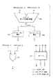
除算及び平方根演算において、スティッキー・ビットは最終部分剰余がゼロであるか否かを確認することによって決定される。所望の数の商ビットを計算した後、最終部分剰余は部分剰余として定義される。部分剰余は冗長形態であるため、桁上げ伝搬加算はゼロ検出前に実施される。図2はスティッキー・ビットを計算するための回路を示す。図2において、最終部分剰余の桁上げ部分201及び和部分202は桁上げ伝搬加算器200によって合計される。加算器200から出力される最上位ビット(Most significant bit;略してmsb)は最終部分剰余の符号ビット203である。図1に示すように、除算ハードウェアは商(即ちQ)及び商−1(即ちQ−1)を累算する。最終部分剰余が負の場合、Q−1は適切な商である。また、最終部分剰余がゼロまたは正の場合、Qは正しい商である。従って、符合ビット203は正しい商を選択すべく使用される。図2において、ゼロ検出器204は非冗長最終部分剰余205の全てのビットがゼロであるか否かを決定し、かつスティッキー・ビット206を出力する。ゼロ検出器204は59入力論理和ゲート(59-input OR gate)と論理的に等しい。
【0020】
一見して、前記の解決策は正または負の最終部分剰余の全ての可能性について適切に見える。しかし、結果が正確である希なケースでは、最終部分剰余は負の除数に等しい。表3は自身によって除される数のための除算反復を示す。ここで、PR[i]はi番目の商デジットが選択された後における部分剰余を示す。
【0021】
【表3】
【0022】
表3に示す第2の反復において、部分剰余PR[1]はゼロである。このため、第2の商デジットは1になる。その後の全ての反復において、部分剰余は負の除数に等しく、−1の商デジットが選択される。最後の反復後、最終部分剰余PR[n]における符合検出は、最終部分剰余が負であることを決定し、かつQ−1を選択すべきことを表示する。事実、これは正しい結果である。しかし、この最終部分剰余はゼロではない。これは不正確な結果を誤って示すとともに、スティッキー・ビットをアサートすべきことを誤って示す。
【0023】
この問題は正確な結果を要する全ての除算演算に波及する。表2に示すように、商選択ロジックは実際にはゼロである部分剰余に対して正の値を予測し、そして同予測を後から補正すべく定義されている。基本的に、前記の問題はこの商選択ロジックの定義に起因して生じる。従来の除算器はスティッキー・ビットの計算前に負の最終部分剰余を復元するために1つのプロセッサ・サイクルを要する。正確なスティッキー・ビット計算の実現が望まれる。負の最終部分剰余を復元することなく正確なスティッキー・ビットの計算を保証する除算器の開発は効果的である。
【0024】
本発明は前述した事情に鑑みてなされたものであって、その目的は、浮動小数点除算及び平方根演算中、最終部分剰余が負の場合にスティッキー・ビットを正確、かつ効果的に計算する能力を提供することにある。本発明の別の目的は商選択規則を実行する際の待ち時間を短縮するとともに、最小限のサイズを有する最適な商選択回路及び同商選択回路を含む除算回路を提供することにある。
【0025】
【課題を解決するための手段】
本発明の課題を解決すべく、2進除算及び平方根演算における商デジットを冗長部分剰余入力に基づいて決定する商デジット選択回路であって、冗長部分剰余入力は第1和ビット、第2和ビット、第3和ビット、第4和ビット及び第5和ビット並びに第1桁上げビット、第2桁上げビット、第3桁上げビット、第4桁上げビット及び第5桁上げビットを含み、選択された商デジットは−1商デジットに該当するマイナス出力(Minus output)と、ゼロ商デジットに該当するゼロ出力(Zero output)と、+1商デジットに該当するプラス出力(Plus output)とのうちのいづれか1つをアサートすることによって出力される商デジット選択回路において、第1和ビット、第2和ビット、第3和ビット及び第4和ビット並びに第1桁上げビット、第2桁上げビット、第3桁上げビット及び第4桁上げビットを入力され、そして第1予測部分剰余ビット、第2予測部分剰余ビット、第3予測部分剰余ビット及び第4予測部分剰余ビットを出力として形成する4ビット桁上げ伝搬加算器と、第1予測部分剰余ビット、第2予測部分剰余ビット、第3予測部分剰余ビット及び第4予測部分剰余ビットを入力され、そしてオール・ゼロ信号を形成し、オール・ゼロ信号は第1予測部分剰余ビット、第2予測部分剰余ビット、第3予測部分剰余ビット及び第4予測部分剰余ビットが全てゼロの場合にのみアサートされる4ビット・ゼロ検出器と、第1予測部分剰余ビット、第2予測部分剰余ビット、第3予測部分剰余ビット及び第4予測部分剰余ビットを入力され、そしてオール・ワン信号を形成し、オール・ワン信号は第1予測部分剰余ビット、第2予測部分剰余ビット、第3予測部分剰余ビット及び第4予測部分剰余ビットが全て1の場合にのみアサートされる4ビット1検出器(Four-bit one detector)と、第5和ビット及び第5桁上げビットを入力され、そして第5ビット・ゼロ信号を形成する否定論理和ゲートと、オール・ワン信号、第5ビット・ゼロ信号及びオール・ゼロ信号を入力され、そしてゼロ出力を形成し、ゼロ出力はオール・ワン信号がアサートされるか、または第5ビット・ゼロ信号及びオール・ゼロ信号の両方がアサートされた場合にのみアサートされるゼロ回路(Zero circuit)とを含む商デジット選択回路が提供される。
【0026】
更に、前記の商デジット選択回路は第1予測部分剰余ビット、オール・ゼロ信号及び第5ビット・ゼロ信号を入力され、そしてプラス出力を形成し、前記プラス出力は第1予測部分剰余ビットがデアサートされ、かつオール・ゼロ信号または第5ビット・ゼロ信号がデアサートされた場合にのみアサートされるプラス回路(Plus circuit)を含み得る。同商デジット選択回路は第1予測部分剰余ビット及びオール・ワン信号を入力され、そしてマイナス出力を形成し、前記マイナス出力は第1予測部分剰余ビットがアサートされ、かつオール・ワン信号がデアサートされた場合にのみアサートされるマイナス回路(Minus circuit)を含み得る。4ビット・ゼロ検出器として4入力論理和ゲート(Four input OR gate)を使用可能である。また、4ビット1検出器は4入力論理積ゲート(Four input AND gate)であり得る。
【0027】
更に本発明では、第1桁上げビット、第2桁上げビット、第3桁上げビット、第4桁上げビット及び第5桁上げビット並びに第1和ビット、第2和ビット、第3和ビット、第4和ビット及び第5和ビットを入力され、そして商デジットを計算する商デジット選択回路であって、第1桁上げビット、第2桁上げビット、第3桁上げビット、第4桁上げビット及び第5桁上げビット並びに第1和ビット、第2和ビット、第3和ビット、第4和ビット及び第5和ビットを入力され、そしてゼロ出力を形成する商ゼロ回路(Quotient zero circuit)と、第1桁上げビット、第2桁上げビット、第3桁上げビット、第4桁上げビット及び第5桁上げビット並びに第1和ビット、第2和ビット、第3和ビット、第4和ビット及び第5和ビットを入力され、そしてプラス出力を形成する商ポジティブ回路(Quotient positive circuit)とを含む商デジット選択回路を提供する。
【0028】
前記の商デジット選択回路は第1桁上げビット、第2桁上げビット、第3桁上げビット及び第4桁上げビット並びに第1和ビット、第2和ビット、第3和ビット及び第4和ビットを入力され、そしてマイナス出力を形成する商ネガティブ回路(Quotient negative circuit)を含み得る。更に商デジット選択回路は、第1桁上げビット、第2桁上げビット、第3桁上げビット、第4桁上げビット及び第5桁上げビット並びに第1和ビット、第2和ビット、第3和ビット、第4和ビット及び第5和ビットを入力され、そして反転されたゼロ出力を形成する反転商ゼロ回路(Inverted quotient zero circuit)と、第1桁上げビット、第2桁上げビット、第3桁上げビット、第4桁上げビット及び第5桁上げビット並びに第1和ビット、第2和ビット、第3和ビット、第4和ビット及び第5和ビットを入力され、そして反転されたプラス出力を形成する反転商ポジティブ回路(Inverted quotient positive circuit)と、第1桁上げビット、第2桁上げビット、第3桁上げビット及び第4桁上げビット並びに第1和ビット、第2和ビット、第3和ビット及び第4和ビットを入力され、そして反転されたマイナス出力を形成する反転商ネガティブ回路(Inverted quotient negative circuit)とを含み得る。
【0029】
更に本発明では、被除数を第1の反復中に入力され、次いで左シフトされた部分剰余をその後の複数の反復中に入力され、そして出力として部分剰余を形成する部分剰余レジスタと、オペランド除数を第1の反復中に入力され、そして出力として除数を形成する除数レジスタと、本発明の商デジット選択回路と、部分剰余と、商デジット及び除数の否定論理積とを入力され、そして左シフトされた部分剰余を形成する加算器とを含む浮動小数点正規形仮数除算回路(Floating point normalized mantissa division circuit)を提供する。同除算回路は商デジットを累算する商レジスタを含み得る。前記の部分剰余は桁上げ部分及び和部分を有する桁上げ保留の形態で表示し得る。また、前記の加算器は桁上げ保留加算器であり得る。
【0030】
更に、2進除算及び平方根演算において商デジットを冗長部分剰余から選択する方法であって、冗長部分剰余は第1和ビット、第2和ビット、第3和ビット、第4和ビット及び第5和ビット並びに第1桁上げビット、第2桁上げビット、第3桁上げビット、第4桁上げビット及び第5桁上げビットを含む方法において、第1予測部分剰余ビット、第2予測部分剰余ビット、第3予測部分剰余ビット及び第4予測部分剰余ビットを形成すべく第1和ビット、第2和ビット、第3和ビット及び第4和ビットを第1桁上げビット、第2桁上げビット、第3桁上げビット及び第4桁上げビットに対して加算する工程と、第1予測部分剰余ビット、第2予測部分剰余ビット、第3予測部分剰余ビット及び第4予測部分剰余ビットが全て1である場合、または前記第1予測部分剰余ビット、第2予測部分剰余ビット、第3予測部分剰余ビット及び第4予測部分剰余ビットが全てゼロであって、かつ第5和ビット及び第5桁上げビットの両方がゼロに等しい場合にのみ商デジットとしてゼロを選択する工程とを含む方法を提供する。
【0031】
更に、前記の商デジットを選択する方法は第1予測部分剰余ビット、第2予測部分剰余ビット、第3予測部分剰余ビット及び第4予測部分剰余ビットが全てゼロにならない状態と、第5和ビット及び第5桁上げビットが全てゼロにならない状態とのうちのいづれかにおいて、第1予測部分剰余ビットがゼロである場合にのみ商デジットとして+1を選択する工程を含み得る。また、同商デジットを選択する方法は第1予測部分剰余ビットがアサートされ、さらには第1予測部分剰余ビット、第2予測部分剰余ビット、第3予測部分剰余ビット及び第4予測部分剰余ビットが全てゼロにならない場合にのみ商デジットとして−1を選択する工程を含み得る。
【0032】
更に本発明では、2進除算及び平方根演算における商デジットを冗長部分剰余入力に基づいて決定する商デジット選択回路を形成する方法であって、冗長部分剰余入力は第1和ビット、第2和ビット、第3和ビット、第4和ビット及び第5和ビット並びに第1桁上げビット、第2桁上げビット、第3桁上げビット、第4桁上げビット及び第5桁上げビットを含み、選択された商デジットは−1商デジットに該当するマイナス出力と、ゼロ商デジットに該当するゼロ出力と、+1商デジットに該当するプラス出力とのうちのいづれか1つをアサートすることによって出力される方法において、第1和ビット、第2和ビット、第3和ビット及び第4和ビット並びに第1桁上げビット、第2桁上げビット、第3桁上げビット及び第4桁上げビットを入力され、そして第1予測部分剰余ビット、第2予測部分剰余ビット、第3予測部分剰余ビット及び第4予測部分剰余ビットを出力として形成する4ビット桁上げ伝搬加算器を形成する工程と、第1予測部分剰余ビット、第2予測部分剰余ビット、第3予測部分剰余ビット及び第4予測部分剰余ビットを入力され、そしてオール・ゼロ信号を形成し、オール・ゼロ信号は第1予測部分剰余ビット、第2予測部分剰余ビット、第3予測部分剰余ビット及び第4予測部分剰余ビットが全てゼロの場合にのみアサートされる4ビット・ゼロ検出器を形成する工程と、第1予測部分剰余ビット、第2予測部分剰余ビット、第3予測部分剰余ビット及び第4予測部分剰余ビットを入力され、そしてオール・ワン信号を形成し、オール・ワン信号は第1予測部分剰余ビット、第2予測部分剰余ビット、第3予測部分剰余ビット及び第4予測部分剰余ビットが全て1の場合にのみアサートされる4ビット1検出器を形成する工程と、第5和ビット及び第5桁上げビットを入力され、そして第5ビット・ゼロ信号を形成する否定論理和ゲートを形成する工程と、オール・ワン信号、第5ビット・ゼロ信号及びオール・ゼロ信号を入力され、そしてゼロ出力を形成し、前記ゼロ出力はオール・ワン信号がアサートされるか、または第5ビット・ゼロ信号及びオール・ゼロ信号の両方がアサートされた場合にのみアサートされるゼロ回路を形成する工程とを含む方法を提供する。
【0033】
前記の商デジット選択回路を形成する方法は第1予測部分剰余ビット、オール・ゼロ信号及び第5ビット・ゼロ信号を入力され、そしてプラス出力を形成し、プラス出力は第1予測部分剰余ビットがデアサートされ、かつオール・ゼロ信号または第5ビット・ゼロ信号がデアサートされた場合にのみアサートされるプラス回路を形成する工程を含み得る。商デジット選択回路は第1予測部分剰余ビット及びオール・ワン信号を入力され、そしてマイナス出力を形成し、マイナス出力は第1予測部分剰余ビットがアサートされ、かつオール・ワン信号がデアサートされた場合にのみアサートされるマイナス回路を形成する工程を含み得る。4ビット・ゼロ検出器として4入力論理和ゲートを使用可能である。また、4ビット1検出器は4入力論理積ゲートであり得る。
【0034】
更に本発明では、第1桁上げビット、第2桁上げビット、第3桁上げビット、第4桁上げビット及び第5桁上げビット並びに第1和ビット、第2和ビット、第3和ビット、第4和ビット及び第5和ビットを入力され、そして商デジットを計算する商デジット選択回路を形成する方法であって、第1桁上げビット、第2桁上げビット、第3桁上げビット、第4桁上げビット及び第5桁上げビット並びに第1和ビット、第2和ビット、第3和ビット、第4和ビット及び第5和ビットを入力され、そしてゼロ出力を形成する商ゼロ回路を形成する工程と、第1桁上げビット、第2桁上げビット、第3桁上げビット、第4桁上げビット及び第5桁上げビット並びに第1和ビット、第2和ビット、第3和ビット、第4和ビット及び第5和ビットを入力され、そしてプラス出力を形成する商ポジティブ回路を形成する工程とを含む方法を提供する。
【0035】
前記の商ポジティブ回路を形成する工程は第1桁上げビット、第2桁上げビット、第3桁上げビット及び第4桁上げビット並びに第1和ビット、第2和ビット、第3和ビット及び第4和ビットを入力され、そしてマイナス出力を形成する商ネガティブ回路を形成する工程を含み得る。
【0036】
更に、前記の商ネガティブ回路を形成する工程は第1桁上げビット、第2桁上げビット、第3桁上げビット、第4桁上げビット及び第5桁上げビット並びに第1和ビット、第2和ビット、第3和ビット、第4和ビット及び第5和ビットを入力され、そして反転されたゼロ出力を形成する反転商ゼロ回路を形成する工程と、第1桁上げビット、第2桁上げビット、第3桁上げビット、第4桁上げビット及び第5桁上げビット並びに第1和ビット、第2和ビット、第3和ビット、第4和ビット及び第5和ビットを入力され、そして反転されたプラス出力を形成する反転商ポジティブ回路を形成する工程と、第1桁上げビット、第2桁上げビット、第3桁上げビット及び第4桁上げビット並びに第1和ビット、第2和ビット、第3和ビット及び第4和ビットを入力され、そして反転されたマイナス出力を形成する反転商ネガティブ回路を形成する工程とを含み得る。
【0037】
また本発明では、被除数を第1の反復中に入力され、次いで左シフトされた部分剰余をその後の複数の反復中に入力され、そして出力として部分剰余を形成する部分剰余レジスタを形成する工程と、オペランド除数を第1の反復中に入力され、そして出力として除数を形成する除数レジスタを形成する工程と、本発明の商デジット選択回路を形成する工程と、部分剰余と、商デジット及び除数の否定論理積とを入力され、そして左シフトされた部分剰余を形成する加算器を形成する工程とを含む浮動小数点正規形仮数除算回路を形成する方法を提供する。同方法は商デジットを累算する商レジスタを形成する工程を含み得る。また、部分剰余は桁上げ部分及び和部分を有する桁上げ保留の形態で表示し得る。更に、加算器は桁上げ保留加算器であり得る。
【0038】
本発明は浮動小数点除算及び平方根演算中、最終部分剰余が負の場合にスティッキー・ビットを正確、かつ効果的に計算する能力を提供する。本発明は本発明に基づく商選択規則を最小限の待ち時間で実行するとともに、最小限のサイズを有する最適な商選択回路を提供する。
【0039】
本発明は正確な結果が得られた際に、作業中の部分剰余が負になることを防止する更に効果的な商デジット選択関数を提供する。負の部分剰余はスティッキー・ビットの計算前に復元する必要がないため、1サイクルが削減される。
【0040】
本発明に基づき、商デジット選択ロジックは負の除数に等しい部分剰余の形成を防止すべく変更される。正確な除算結果を実現する正確、かつ効果的なスティッキー・ビットの計算を行うために、負の除数に等しい負の部分剰余の形成を防止する必要がある。これを実現すべく商デジット選択関数を強化して、ハードウェアのコストの削減及び待ち時間の短縮を行い得る。このため、商デジット選択関数の強化は理想的な解決策である。予備最終部分剰余(Preliminary final partial remainder)を復元するための余分なメカニズムを提供する必要がないため、余分なハードウェアが排除される。負の予備部分剰余を復元する別のサイクル時間を必要としないため、待ち時間が短縮される。
【0041】
本発明に基づき、実際の部分剰余がゼロの際に、1の商デジットに変えてゼロの商デジットを選択すべく商デジット選択ロジックが変更される。上位4ビットがゼロである5ビットからなる予測部分剰余を使用することにより、第4の上位ビットへの可能な桁上げ伝搬が検出される。これは冗長部分剰余のうちの第5の最上位和ビット及び桁上げビットの確認により実現可能である。これら両方がゼロである場合、同ビット位置から予測部分剰余の最下位ビット位置への桁上げ伝搬は不可能であり、ゼロの商デジットが選択される。冗長部分剰余の第5の最上位桁上げビット及び和ビットのうちの少なくともいづれか一方が1である別のケースでは、1の商デジットが選択される。
【0042】
【発明の実施の形態】
浮動小数点演算において、負の最終部分剰余が生じた際にスティッキー・ビットを正確に計算すべく幾つかのオプションを検討する必要がある。最も簡単な解決策はゼロ検出を行う前に除数を加算することにより、負の最終部分剰余を復元することが挙げられる。別の桁上げ伝搬加算器を設置するために要する空間を考慮した場合、解決策は従来のハードウェアを利用する必要がある。これを実現する2つの方法を図3及び図4に示す。
【0043】
図3に示す解決策は基本的な反復工程をインプリメントする従来の桁上げ保留加算器300を利用している。通常の演算中、最終サイクル信号301はロー(Low)である。この結果、マルチプレクサ302,303は図1に関連して詳述した標準的反復工程をインプリメントすべく形成されている。しかし、最終サイクル中、最終サイクル信号301はハイ(High)であり、マルチプレクサ303はレジスタ305内に格納された部分剰余の桁上げ部分及び和部分に対して除数D304を加算すべく同除数D304を加算器300へ出力する。予備部分剰余の符号が負の場合、マルチプレクサ306は加算器300の結果を最終部分剰余フリップ・フロップ307に対して出力する。
【0044】
図4に示す解決策では、図2に示すスティッキー・ビット計算を行う従来の桁上げ伝搬加算器400を再び使用している。図1に示す反復データパス等のデータパスが所望の精度の商デジットを形成した後、冗長部分剰余の桁上げ部分PRC及び和部分PRSは最終サイクル信号がローの間にマルチプレクサ403,402へそれぞれ入力される。次いで、桁上げ伝搬加算器400は冗長部分剰余を予備非冗長最終部分剰余(Preliminary non-redundant final partial remainder)へと削減する。桁上げ伝搬加算器400の最上位出力ビット404は予備最終部分剰余の符号を示す。非冗長予備最終部分剰余はフリップ・フロップ406内へラッチされる。次いで、最終サイクル信号401がアサートされる。予備最終部分剰余が負であることを符号ビット404が示した場合、マルチプレクサ405は加算器400に対して除数を出力するマルチプレクサ402に対して同除数を出力する。その一方、マルチプレクサ403は加算器400に対する別の入力として予備非冗長部分剰余を出力する。次いで、ゼロ検出器407は復元された部分剰余を使用してスティッキー・ビットを形成する。符号ビットが負以外の部分剰余を示す場合、マルチプレクサ405は除数Dに代えてゼロを部分剰余に対して加算させる。
【0045】
図3及び図4に示す前記の2つの解決策は、予備最終部分剰余が負の際にスティッキー・ビットを計算すべく別のマルチプレクサ・ハードウェアと、別のサイクルとを要する。マルチプレクサ302は部分剰余形成クリティカル・パス(Partial remainder formation critical path)上に配置されている。このため、図3に示す解決策は基本的反復のためのサイクル時間に影響を及ぼす。更に、パイプライン・スーパースカラ・プロセッサ内の待ち時間可変命令(Variable latency instructions)は命令スケジューリング及びバイパス制御ロジックを更に複雑にするため望ましくない。従って、スティッキー・ビットを正確に計算するために除算演算の全分布のうちの僅かな部分のみが余分なサイクルを必要とする場合にも、負の予備最終部分剰余を形成しない除算命令のための余分なサイクルを削除すべくプロセッサのデザインは更に複雑になる。従って、負の部分剰余を復元する正味の効果は、全ての除算及び平方根演算を行う別の待ち時間サイクルを必要とする。
【0046】
本発明に基づき、商デジット選択ロジックは負の除数に等しい部分剰余の形成を防止するために変更される。正確な除算結果を実現するスティッキー・ビットを正確、かつ効果的に計算すべく、負の除数に等しい負の部分剰余の形成を防止する必要がある。これを実現すべく商デジット選択関数を強化することにより、ハードウェアが削減され、かつ待ち時間が短縮される。このため、同選択関数の強化は理想的な解決策である。予備最終部分剰余を復元するための余分なメカニズムを提供する必要がないため、余分なハードウェアを排除し得る。また、負の予備部分剰余を復元する別のサイクル時間を必要としないため待ち時間が短縮される。
【0047】
本発明に基づく、商デジット選択ロジックは、実際の部分剰余がゼロの際に1の商デジットに代えてゼロの商デジットを選択すべく変更される。これは2PR[i]est=000.0に対してq[i+1]=0を選択することを示唆している。しかし、商デジット選択関数は実際の部分剰余より寧ろ予測部分剰余に対して作用するため、商選択ロジックの注意深いデザインが必要である。実際には予測部分剰余は1/2未満であり得るため、更に下位の冗長部分剰余ビットの加算は実際の部分剰余の上位4ビットのうちの最下位ビット位置へ1を伝搬させる。従って、実際の部分剰余は1/2以上になる。
【0048】
実際の部分剰余が1/2(または1/2以上)である場合、除数は1/2≦D<1に限定されるため、q=1を常に選択する必要がある。実際の部分剰余が1/2より更に大きく、かつq=0が選択された場合、次の部分剰余は除数を最初に加算または減算することなく、実際の部分剰余を左側へ1ビットだけシフトすることによって得られる。この左シフトは正確な商への収束に必要な3/2の上限を越える次の実際の部分剰余を形成する。
【0049】
正確な商デジットがゼロの際に、除数が実際の部分剰余より更に大きく、さらに商デジットとして+1の値が選択された場合、このエラーは後の反復において補正可能である。しかし、予測部分剰余が000.0であって、かつ正確な商デジットが1である際に商デジットとしてゼロが選択された場合、このエラーを補正する方法はない。q=1が正しい商デジットである際にq=0が選択された場合、過小予測を補正する方法はない。結果は回復不能な誤りであり、次の部分剰余は正確な結果への収束に必要な所定の上下限の外に位置する。
【0050】
全ての部分剰余に対する2進加算の実施は予測の問題を排除する。しかし、これはSRT除算のタイミング及び空間に関する効果を無効にする。ゼロの商デジットは全ての部分剰余がゼロである際にのみ選択可能である。しかし、全ての部分剰余に対するゼロの検出は同一の理由により逆効果となる。
【0051】
前記の解決策に対する簡単な代替策としては、実際の部分剰余の上位4ビットのうちの最下位ビットへの可能な桁上げ伝搬を検出することが挙げられる。これは冗長部分剰余のうちの第5の最上位和ビット及び桁上げビット、即ちPRS,msb-4及びPRC,msb-4を確認することによって実現し得る。PRS,msb-4及びPRC,msb-4がそれぞれゼロである場合、そのビット位置から予測部分剰余の最下位ビット位置への桁上げ伝搬は不可能であり、さらにはゼロの商デジットを選択する必要がある。冗長部分剰余の第5の最上位桁上げビット及び和ビットのうちの少なくともいづれか一方が1である別のケースでは、1の商デジットを選択する必要がある。部分剰余のうちの複数の下位ビットがゼロでない場合にも、同部分剰余は所定の上下限(−5/2≦2PR≦3/2)内に存在し、かつ正しい結果が依然算出されることになる。
【0052】
予測部分剰余の計算に必要な桁上げ伝搬加算は実際の冗長部分剰余の上位4つの伝搬ビット及び和ビットに対してのみ行われる。このため、本発明に基づく計算の待ち時間に対する影響は最低限に抑制される。表4は本発明に基づく正確な商選択ロジックのための真理値表を示す。
【0053】
【表4】
【0054】
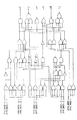
ランダム・ロジック504のブロックはSRT除算に基づく可能な商デジット値のうちの1つにそれぞれ該当する3つの信号(M、Z及びP)を形成する。Mは−1の商デジットに該当する。Zはゼロの商デジットに該当する。Pは+1の商デジットに該当する。Mはx[3]がデアサートされ、かつn1がデアサートされた場合にのみアサートされる。Zはn1がアサートされるか、またはi0及びn0がアサートされた場合にのみアサートされる。PはX[3]がアサートされ、n0またはi0がデアサートされた場合にのみアサートされる。各論理関係を仮定した場合、商デジット信号M、Z及びPのうちの任意の2つを同時にアサートすることは不可能である。
【0055】
図5に示すインプリメンテーションは論理的に正しい。しかし実際には、4ビット2進加算器及びその後のロジックは統合され、さらには最適化されたロジック・インプリメンテーションへの併合が可能である。図6に示すように、5段階ロジック・インプリメンテーション(Five-stage logic implementation)は空間を更に効果的に使用するとともに、出力を更に短い遅延時間を伴って形成する。
【0056】
図6に示すインプリメンテーションでは、M、Z及びPが計算されるとともに、論理反転/M、/Z及び/Pも計算される。これはデコードされた選択入力を有するCMOSマルチプレクサ内等において伝達ゲートをイネーブルするために商信号を使用する際に効果的である。M及び/Mは冗長部分剰余ビットの上位4ビット(2PRC[msb:msb−3]及び2PRS[msb:msb−3])にのみ依存する。その一方、Z、P、/Z及び/Pは全て冗長部分剰余の上位5ビット(2PRC[msb:msb−4]及び2PRS[msb:msb−4])に依存する。図6のセルは回路が占める空間の削減を第2の課題とする一方で、主に遅延を最小限に抑制すべく最適化されている。図6に示す殆どの論理は空間を削減すべく幾つかの出力計算の間において共有されている。
【0057】
本発明に基づく基数2を使用する新たな商デジット選択論理(Radix-2 quotient digit selection logic)をインプリメントするために必要な別のゲートの総数は比較的少ない。好ましい実施の形態のインプリメンテーションに関するスパイス・シミュレーション分析(Spice simulation analysis)において、商選択論理クリティカル・タイミング・パス(Quotient selection logic critical timing path)が5%未満であることが示されている。
【0058】
更に遅い商選択ロジックと、最後に行われる部分剰余復元サイクルの排除との間には、インプリメンテーションに依存するタイミング・トレードオフが存在する。僅かにより複雑な商選択論理に起因する遅延の増加がプロセッサ・サイクル時間(Processor cycle time)を制限しない場合、性能の増加は負の最終部分剰余の復元に必要とされる待ち時間サイクルの削減により常には実現される。本発明のハードウェア除算器等を含む最近のマイクロプロセッサでは、プロセッサ・サイクル時間は他のクリティカル・パスによって決定されるか、またはプロセッサを設計する前に任意で適合させ得る。商選択ロジックのうちの増大した遅延が最長パスでないケースにおいて、各除算演算あたり1サイクルの正味節約は新たな出費を伴うことなく実現し得る。
【0059】
図6に示す実施の形態において、変更された商選択ロジック・アルゴリズムは内部浮動小数点除算器クリティカル・パス(Internal floating point divider critical path)の速度を従来の商選択規則を使用して最適化された同等のクリティカル・パスより約100ps遅くする。これは2パーセント未満の速度低下に相当する。プロセッサの限界タイミング・パス(Limiting timing path)は更に長い。従って、改善された商選択ロジックはプロセッサ・サイクル時間に悪影響を及ぼさない。スティッキー検出(Sticky detection)前に部分剰余を復元するサイクルを排除する効果が実現される。
【0060】
本発明の商選択ロジックを使用しても負の最終部分剰余は依然形成され得る。しかし、負の最終部分剰余が形成された際、本発明に基づく商選択ロジックは負の部分剰余が負の除数より更に大きいことを保証する。従って、本発明に基づく負の最終部分剰余が形成された場合、Q−1が選択され、結果は必ず不正確になる。この結果、負の最終部分剰余が負の除数に等しくなる恐れを伴うことなくスティッキー・ビットを安全にアサートし得る。
【0061】
符号検出及びスティッキー・ビット計算を平行して実施する一方で、ハードウェアの節約が可能である。59ビット全加算器を使用する代わりに、59ビット符号検出加算器(59-bit sign detect adder)を使用し得る。これはタイミングを僅かに改善する一方で、主に空間の節約を実現する。ゼロ検出は冗長部分剰余を2進数へ変換する明確な加算を伴うことなく行える。
【0062】
【数4】
【0063】
【数5】
【0064】
以上、本発明を好ましい実施の形態に基づいて詳述したが、同実施の形態は例示を目的とするものであって、本発明を限定するものではない。当業者は必要に応じて本発明の実施の形態を変更することが可能であり、同変更は請求項に開示する本発明の範囲及び精神を逸脱しないものとする。例えば、図6に示す商選択ロジックの最適化された論理インプリメンテーションは各種の同等の方法を用いて設計し得る。また、図6に示す回路は標準的なCMOS伝達ゲート・マルチプレクサ(CMOS transmission gate multiplexor)に代えて、n−チャネル・パス・トランジスタ・マルチプレクサ(n-channel pass transistor multiplexor)を制御すべく商デジットの正の極性のみを計算し、論理反転の計算を削除できる。最適化された異なるインプリメンテーションは異なる技術(例:NMOS、ECL等)におけるインプリメンテーション、または同一技術に属する異なる設計規則及び設計ツールを用いたインプリメンテーションの結果である。請求項は表4に示す真理値表の全ての回路インプリメンテーションを網羅することを目的とする。従って、本発明の技術分野の当業者にとって自明な各種の変更及び修正は、本発明の精神及び範囲に属する。
【0065】
【発明の効果】
以上詳述したように、本発明によれば、浮動小数点除算及び平方根演算中、最終部分剰余が負の場合にスティッキー・ビットを正確、かつ効果的に計算し得る。更に、本発明は商選択規則を実行する際の待ち時間を短縮するとともに、最小限のサイズを有する最適な商選択回路及び同商選択回路を含む除算回路を実現するという優れた効果を発揮する。
【図面の簡単な説明】
【図1】反復SRT除算アルゴリズムをインプリメントする従来のハードウェア除算モジュールの簡単な論理図。
【図2】従来のスティッキー・ビット演算回路の簡単な論理図。
【図3】反復SRT除算アルゴリズムをインプリメントするか、または負の最終部分剰余を復元する1つのハードウェア除算モジュールの簡単な論理図。
【図4】反復SRT除算アルゴリズムをインプリメントするか、または負の最終部分剰余を復元する別のハードウェア除算モジュールの簡単な論理図。
【図5】本発明の商選択規則をインプリメントする回路の簡単な論理図。
【図6】商デジット信号及びその論理反転を形成する商選択規則をインプリメントする回路の詳細な論理図。
【符号の説明】
300…桁上げ保留加算器、301,401…最終サイクル信号、302,303,306,403,402,405…マルチプレクサ、304…除数、305…レジスタ、307,406…フリップ・フロップ、400…桁上げ伝搬加算器、404…最上位出力ビット、404…符号ビット、407…ゼロ検出器、500…4ビット桁上げ伝搬加算器、501…オール・ゼロ検出器、502…オール・ワン検出器、503…否定論理和ゲート、504…ランダム・ロジック。[0001]
BACKGROUND OF THE INVENTION
The present invention relates to the field of floating point dividers in microprocessors, and more particularly to quotient digit selection rules in SRT division / square root implementations. For rules, the rule prevents the formation of negative final partial remainders if the result is accurate.
[0002]
[Prior art and problems to be solved by the invention]
The SRT algorithm provides one way to perform non-restoring division. The details are described in J. Ann., Published in September 1958, published in the American Institute of Electrical and Electronics Engineers Computer Division (IEEE Trans. Comput.) C-7, 218-222. E. Described in Robertson's “New Class of Digital Division” and published in 1958, Quart. J. Mech. Appl. Math., 11th issue,
[0003]
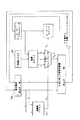
If the radix is larger, the number of quotient digits formed in one iteration is even greater. This increases complexity. A radix-2 implementation forms one digit in one iteration. A radix-4 implementation forms two digits in one iteration. FIG. 1 shows a simple SRT radix-2 floating point implementation using radix-2 based on SRT. The implementation requires that both the divisor and the dividend are positive and normalized. Therefore, 1/2 ≦ D and dividend <1. The initial shifted partial remainder, 2PR [0], is the dividend. The dividend is loaded into the
[0004]
[Expression 1]
[0005]
The partial remainder is generally maintained in the form of redundant carry reserve. As a result, in the next partial remainder calculation, the processing speed is further slow, and a carry hold adder can be used instead of a large carry propagation adder. The partial remainder is converted to a non-redundant form after all iterations have been performed and the desired accuracy has been achieved. The SRT algorithm allows over prediction of quotient digits. Due to overestimation of the quotient digit, a negative partial remainder is subsequently formed. For this reason, the last quotient digit can be overestimated to make the final partial remainder negative. In this case, since it is impossible to correct the excessive prediction, it is necessary to maintain Q and Q-1. As a result, when the final partial remainder is negative, Q-1 is selected instead of Q. The quotient digit is always maintained in a redundant form, and further converted to a non-redundant form in the last iteration. Instead, the quotient (ie, Q) and quotient-1 (ie, Q-1) are published in the American Institute of Electrical and Electronics Engineers Computer Society (IEEE Trans. Comput.) Vol. 41, Vol. 12, published in December 1992. M. described on pages 1497 to 1503. Di. Elsegoback and Tee. It can be formed on a fly based on the rules disclosed in “On-the-fly rounding” by Lang.
[0006]
The SRT algorithm is also applied to the square root operation. This allows the use of conventional division hardware. The simplified square root formula is similar to the division formula. This is described in M.P. 1016 to 1024 of Vol. 39, No. 8 of the Institute of Electrical and Computer Engineers (IEEE Trans. Comput.) Published in August 1990. Di. Elsegoback and Tee. See Lang's "Radix-4 square root without initial PLA". The iterative equation for the square root operation is shown in
[0007]
[Expression 2]
[0008]
The binary division algorithm is similar to the standard decimal division taught at grammar school. Each quotient digit for Q is predicted at R / D = Q. To determine the first quotient digit, the appropriate predicted value of the quotient digit is multiplied by a divisor. The product is then subtracted from the dividend to form a remainder. If the remainder is larger than the divisor, the predicted value of the quotient digit is too small. Furthermore, when the remainder is negative, the predicted value of the quotient digit is excessive. In any case, if the predicted value of the quotient digit is incorrect, it is necessary to change the predicted value. As a result, the correct quotient digit is derived before proceeding to the next digit. The quotient digit is correct if the following relationship is true: 0 ≦ PR <D. Here, PR indicates the partial remainder after subtracting the quotient digit multiplied by the divisor.
[0009]
The key to the SRT division algorithm is that negative quotient digits can be used. For example, in
[0010]
It is guaranteed that the above criteria for maintaining the partial residue within a predetermined upper and lower limit can be satisfied without using all partial residue digits. In order to select a quotient digit that enables calculation of a correct operation result, only a few upper digits of the partial residue need be used.
[0011]
SRT division requires a final addition after selection of all quotient digits in order to reduce the redundant quotient representation to a standard non-redundant form with only non-negative digits.
In the binary system (base 2) used in modern electronic computing circuits, SRT division provides +1, 0 or -1 quotient digits. The
[0012]
[Equation 3]
[0013]
Forecast partial remainder (PR est ) Can be calculated using only a 4-bit carry propagation adder. The 4-bit carry propagation adder adds the upper 4 bits of the carry part and the sum part of the actual partial remainder. Calculation of the upper 4 bits of the actual partial remainder requires 59-bit carry propagation full addition. This simplification therefore means a significant savings in latency. Prediction partial remainder PR est Does not indicate the possibility that the carry is propagated to the bit position that matches the least significant bit position in the predicted partial remainder when 59-bit carry propagation full addition is performed. Table 1 is a truth table for conventional quotient
[0014]
[Table 1]
[0015]
The quotient selection logic is designed to correctly predict or overestimate the true quotient result, such as predicting 1 instead of 0, or 0 instead of -1. If the SRT algorithm selects an incorrect quotient digit, it corrects itself later.
[0016]
The partial remainder is limited to −5 / 2 ≦ 2PR [i] ≦ 3/2. For this reason, the conventional truth table for quotient selection logic (SRT radix-2 quotient selection logic) using radix-2 based on SRT has several don't care inputs. Since the lower bits are ignored, the predicted partial residue is always less than or equal to the most significant upper bit of the true partial residue. Therefore, there is one case (indicated by an asterisk in the above truth table) where the predicted partial remainder is outside the upper and lower limits. The implemented SRT algorithm does not form a partial remainder outside the upper and lower limits. For this reason, the actual partial remainder is within the negative limit. Accordingly, -1 is an appropriate quotient digit to be selected. There are two other cases where the quotient digit selected based on the predicted partial residue is different from the quotient digit selected based on the actual partial residue (corresponding to the entries for 111.0 and 111.1 in Table 1). Exists. However, in the wrong example of quotient digit selection shown here, the quotient digit is not underestimated and the partial remainder is maintained within a predetermined upper and lower limit. Thus, the final result is still accurately formed.
[0017]
Table 2 below is a truth table that simply represents the conventional quotient selection logic shown in Table 1. In the following table, “X” represents a “Don't care” logic variable. 1xx. The third case where x forms a quotient digit of −1 does not apply when the predicted partial remainder is 111.1. In this case, the second entry is used and the correct quotient digit is zero.
[0018]
[Table 2]
[0019]
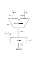
In division and square root operations, the sticky bit is determined by checking whether the final partial remainder is zero. After calculating the desired number of quotient bits, the final partial remainder is defined as the partial remainder. Since the partial remainder is in a redundant form, carry propagation addition is performed before zero detection. FIG. 2 shows a circuit for calculating sticky bits. In FIG. 2, the
[0020]
At first glance, the above solution seems appropriate for all possible positive or negative final partial residues. However, in the rare case where the result is accurate, the final partial remainder is equal to a negative divisor. Table 3 shows the division iteration for the number divided by itself. Here, PR [i] indicates a partial remainder after the i-th quotient digit is selected.
[0021]
[Table 3]
[0022]
In the second iteration shown in Table 3, the partial remainder PR [1] is zero. For this reason, the second quotient digit is 1. In all subsequent iterations, the partial remainder is equal to the negative divisor and the −1 quotient digit is selected. After the last iteration, sign detection in the final partial residue PR [n] indicates that the final partial residue is negative and that Q-1 should be selected. In fact, this is the correct result. However, this final partial remainder is not zero. This falsely indicates an inaccurate result and falsely indicates that the sticky bit should be asserted.
[0023]
This problem affects all division operations that require accurate results. As shown in Table 2, the quotient selection logic is defined to predict a positive value for a partial remainder that is actually zero, and to later correct the prediction. Basically, the above problem arises due to the definition of this quotient selection logic. Conventional dividers require one processor cycle to restore the negative final partial remainder before calculating the sticky bits. Realization of accurate sticky bit calculation is desired. It is effective to develop a divider that guarantees accurate sticky bit computation without restoring the negative final partial remainder.
[0024]
The present invention has been made in view of the circumstances described above, and its purpose is to provide an ability to accurately and effectively calculate sticky bits when the final partial remainder is negative during floating point division and square root operations. It is to provide. Another object of the present invention is to provide an optimum quotient selection circuit having a minimum size and a division circuit including the quotient selection circuit while reducing the waiting time when executing the quotient selection rule.
[0025]
[Means for Solving the Problems]
In order to solve the problems of the present invention, a quotient digit selection circuit for determining a quotient digit in binary division and square root operation based on a redundant partial remainder input, the redundant partial remainder input being a first sum bit and a second sum bit , 3rd sum bit, 4th sum bit and 5th sum bit and 1st carry bit, 2nd carry bit, 3rd carry bit, 4th carry bit and 5th carry bit are selected and selected The quotient digit is either a minus output (Minus output) corresponding to the -1 quotient digit, a zero output corresponding to the zero quotient digit, or a plus output (Plus output) corresponding to the +1 quotient digit. In the quotient digit selection circuit output by asserting one, the first sum bit, the second sum bit, the third sum bit and the fourth sum bit, the first carry bit, and the second carry bit , The third carry bit and the fourth carry bit are input, and the first prediction partial remainder bit, the second prediction partial remainder bit, the third prediction partial remainder bit and the fourth prediction partial remainder bit are formed as outputs. A 4-bit carry propagation adder, a first prediction partial remainder bit, a second prediction partial remainder bit, a third prediction partial remainder bit, and a fourth prediction partial remainder bit, and form an all-zero signal; A 4-bit zero detector that is asserted only when the first predicted partial remainder bit, the second predicted partial residual bit, the third predicted partial residual bit, and the fourth predicted partial residual bit are all zero; The first prediction partial residue bit, the second prediction partial residue bit, the third prediction partial residue bit, and the fourth prediction partial residue bit are input and form an all-one signal, The 4-
[0026]
Further, the quotient digit selection circuit is input with a first predicted partial remainder bit, an all zero signal and a fifth bit zero signal, and forms a positive output, and the positive output is deasserted by the first predicted partial remainder bit. And a plus circuit that is asserted only when the all zero signal or the fifth bit zero signal is deasserted. The quotient digit selection circuit receives a first predicted partial remainder bit and an all-one signal and forms a negative output, the negative output having the first predicted partial remainder bit asserted and the all-one signal deasserted. Minus circuit that is asserted only when As a 4-bit zero detector, a 4-input OR gate can be used. The 4-
[0027]
Furthermore, in the present invention, the first carry bit, the second carry bit, the third carry bit, the fourth carry bit and the fifth carry bit, the first sum bit, the second sum bit, the third sum bit, A quotient digit selection circuit for inputting a fourth sum bit and a fifth sum bit and calculating a quotient digit, the first carry bit, the second carry bit, the third carry bit, and the fourth carry bit A quotient zero circuit which receives the fifth carry bit and the first sum bit, the second sum bit, the third sum bit, the fourth sum bit and the fifth sum bit and forms a zero output; 1st carry bit, 2nd carry bit, 3rd carry bit, 4th carry bit, 5th carry bit, 1st sum bit, 2nd sum bit, 3rd sum bit, 4th sum bit And the fifth sum bit, and Providing quotient digit selection circuit including a quotient positive circuit (Quotient positive circuit) to form a class output.
[0028]
The quotient digit selection circuit includes a first carry bit, a second carry bit, a third carry bit, a fourth carry bit, a first sum bit, a second sum bit, a third sum bit, and a fourth sum bit. And a quotient negative circuit that forms a negative output. Further, the quotient digit selection circuit includes a first carry bit, a second carry bit, a third carry bit, a fourth carry bit, a fifth carry bit, a first sum bit, a second sum bit, and a third sum. Bit, 4th sum bit and 5th sum bit, and an inverted quotient zero circuit that forms an inverted zero output, a first carry bit, a second carry bit, a third Carry bit, 4th carry bit and 5th carry bit and first sum bit, second sum bit, third sum bit, fourth sum bit and fifth sum bit are inputted and inverted plus output An inverted quotient positive circuit, and a first carry bit, a second carry bit, a third carry bit, a fourth carry bit, a first sum bit, a second sum bit, 3 sum bits and And an inverted quotient negative circuit that receives the fourth sum bit and forms an inverted negative output.
[0029]
Further, in the present invention, the dividend is input during the first iteration, then the left-shifted partial remainder is input during subsequent iterations, and the partial remainder register forms the partial remainder as an output, and the operand divisor. A divisor register that is input during the first iteration and forms a divisor as an output, a quotient digit selection circuit of the present invention, a partial remainder, and a negative AND of the quotient digit and the divisor is input and left shifted And a floating point normalized mantissa division circuit including an adder that forms a partial remainder. The division circuit may include a quotient register that accumulates the quotient digit. The partial remainder may be displayed in the form of a carry hold having a carry portion and a sum portion. The adder may be a carry reserve adder.
[0030]
Further, a method of selecting a quotient digit from redundant partial remainders in binary division and square root operations, wherein the redundant partial remainders are a first sum bit, a second sum bit, a third sum bit, a fourth sum bit, and a fifth sum. A method including a bit and a first carry bit, a second carry bit, a third carry bit, a fourth carry bit, and a fifth carry bit, a first predicted partial remainder bit, a second predicted partial remainder bit, A first sum bit, a second sum bit, a third sum bit and a fourth sum bit to form a third predicted partial remainder bit and a fourth predicted partial remainder bit; The step of adding to the third carry bit and the fourth carry bit, and the first prediction partial remainder bit, the second prediction partial remainder bit, the third prediction partial remainder bit, and the fourth prediction partial remainder bit are all 1. If The first prediction partial remainder bit, the second prediction partial remainder bit, the third prediction partial remainder bit, and the fourth prediction partial remainder bit are all zero, and both the fifth sum bit and the fifth carry bit are And selecting zero as the quotient digit only if it is equal to zero.
[0031]
Further, the method of selecting the quotient digit includes a state in which the first prediction partial remainder bit, the second prediction partial remainder bit, the third prediction partial remainder bit, and the fourth prediction partial remainder bit are not all zero, and a fifth sum bit. And selecting the +1 as the quotient digit only if the first predicted partial remainder bit is zero, either in the case where the fifth carry bit is not all zero. The method of selecting the quotient digit is that the first prediction partial remainder bit is asserted, and further, the first prediction partial remainder bit, the second prediction partial remainder bit, the third prediction partial remainder bit, and the fourth prediction partial remainder bit are It may include selecting -1 as the quotient digit only if it is not all zero.
[0032]
The present invention further provides a method of forming a quotient digit selection circuit for determining a quotient digit in binary division and square root operation based on a redundant partial remainder input, wherein the redundant partial remainder input is a first sum bit, a second sum bit , 3rd sum bit, 4th sum bit and 5th sum bit and 1st carry bit, 2nd carry bit, 3rd carry bit, 4th carry bit and 5th carry bit are selected and selected The quotient digit is output by asserting one of a negative output corresponding to a -1 quotient digit, a zero output corresponding to a zero quotient digit, and a positive output corresponding to a +1 quotient digit. , 1st sum bit, 2nd sum bit, 3rd sum bit and 4th sum bit, 1st carry bit, 2nd carry bit, 3rd carry bit and 4th carry bit Forming a 4-bit carry propagation adder configured to output and output a first prediction partial residue bit, a second prediction partial residue bit, a third prediction partial residue bit, and a fourth prediction partial residue bit; 1 prediction partial residue bit, 2nd prediction partial residue bit, 3rd prediction partial residue bit, and 4th prediction partial residue bit are input and form an all-zero signal, the all-zero signal being the first prediction partial residue bit Forming a 4-bit zero detector that is asserted only when the second predicted partial remainder bit, the third predicted partial residual bit, and the fourth predicted partial residual bit are all zero, The second prediction partial remainder bit, the third prediction partial remainder bit, and the fourth prediction partial remainder bit are input and form an all-one signal, and the all-one signal is the first prediction partial remainder bit. Forming a 4-
[0033]
The method of forming the quotient digit selection circuit receives a first predicted partial remainder bit, an all zero signal, and a fifth bit zero signal, and forms a positive output, where the positive output is the first predicted partial remainder bit. Forming a plus circuit that is deasserted and asserted only when the all zero signal or the fifth bit zero signal is deasserted. The quotient digit selection circuit receives the first predicted partial remainder bit and the all-one signal and forms a negative output, where the negative output is when the first predicted partial remainder bit is asserted and the all-one signal is deasserted Forming a negative circuit that is asserted only at a time. A 4-input OR gate can be used as a 4-bit zero detector. Also, the 4-
[0034]
Furthermore, in the present invention, the first carry bit, the second carry bit, the third carry bit, the fourth carry bit and the fifth carry bit, the first sum bit, the second sum bit, the third sum bit, A method of forming a quotient digit selection circuit that receives a fourth sum bit and a fifth sum bit and calculates a quotient digit, the first carry bit, the second carry bit, the third carry bit, 4th carry bit and 5th carry bit and 1st sum bit, 2nd sum bit, 3rd sum bit, 4th sum bit and 5th sum bit are inputted, and a quotient zero circuit forming a zero output is formed A first carry bit, a second carry bit, a third carry bit, a fourth carry bit, a fifth carry bit, a first sum bit, a second sum bit, a third sum bit, 4th sum bit and 5th sum bit are input And the method comprising the steps of forming a quotient positive circuit forming the positive output.
[0035]
The step of forming the quotient positive circuit includes a first carry bit, a second carry bit, a third carry bit, a fourth carry bit, a first sum bit, a second sum bit, a third sum bit, and a second carry bit. It may include forming a quotient negative circuit that is input with 4 sum bits and forms a negative output.
[0036]
Further, the step of forming the quotient negative circuit includes a first carry bit, a second carry bit, a third carry bit, a fourth carry bit, a fifth carry bit, a first sum bit, and a second sum. Forming an inverted quotient zero circuit receiving the bit, the third sum bit, the fourth sum bit and the fifth sum bit and forming an inverted zero output; a first carry bit; a second carry bit , Third carry bit, fourth carry bit and fifth carry bit and first sum bit, second sum bit, third sum bit, fourth sum bit and fifth sum bit are inputted and inverted Forming an inverted quotient positive circuit for forming a positive output, a first carry bit, a second carry bit, a third carry bit, a fourth carry bit, a first sum bit, a second sum bit, 3rd sum bit and 4th It is input to the bit, and may include the step of forming the inverted quotient negative circuit for forming an inverted negative output.
[0037]
The present invention also provides a step of forming a partial remainder register in which the dividend is input during a first iteration and then the left-shifted partial remainder is input during subsequent iterations and forms a partial remainder as an output. Forming a divisor register in which an operand divisor is input during the first iteration and forming a divisor as an output; forming a quotient digit selection circuit of the present invention; a partial remainder; a quotient digit and a divisor A method of forming a floating point normal mantissa division circuit including the step of forming an adder that receives a negative AND and forms a left-shifted partial remainder. The method may include forming a quotient register that accumulates quotient digits. Also, the partial remainder can be displayed in the form of a carry hold having a carry portion and a sum portion. Further, the adder may be a carry hold adder.
[0038]
The present invention provides the ability to accurately and effectively compute sticky bits during floating point division and square root operations when the final partial remainder is negative. The present invention provides an optimal quotient selection circuit having a minimum size while executing a quotient selection rule according to the present invention with a minimum latency.
[0039]
The present invention provides a more effective quotient digit selection function that prevents the partial remainder in operation from becoming negative when accurate results are obtained. One cycle is reduced because the negative partial remainder does not need to be restored before calculating the sticky bits.
[0040]
In accordance with the present invention, the quotient digit selection logic is modified to prevent the formation of a partial remainder equal to the negative divisor. In order to perform an accurate and effective sticky bit calculation that achieves an accurate division result, it is necessary to prevent the formation of a negative partial remainder equal to the negative divisor. To achieve this, the quotient digit selection function can be enhanced to reduce hardware costs and latency. For this reason, enhancing the quotient digit selection function is an ideal solution. Extra hardware is eliminated because there is no need to provide an extra mechanism to restore the Preliminary final partial remainder. Latency is reduced because no separate cycle time is needed to restore the negative spare partial remainder.
[0041]
In accordance with the present invention, when the actual partial remainder is zero, the quotient digit selection logic is changed to select a quotient digit of zero instead of one quotient digit. By using a predicted partial remainder consisting of 5 bits where the upper 4 bits are zero, possible carry propagation to the fourth upper bit is detected. This can be realized by checking the fifth most significant sum bit and carry bit of the redundant partial remainder. If both are zero, carry propagation from the same bit position to the least significant bit position of the predicted partial remainder is not possible and a quotient digit of zero is selected. In another case where at least one of the fifth most significant carry bit and the sum bit of the redundant partial remainder is 1, a quotient digit of 1 is selected.
[0042]
DETAILED DESCRIPTION OF THE INVENTION
In floating point operations, several options need to be considered to accurately calculate sticky bits when a negative final partial remainder occurs. The simplest solution is to restore the negative final partial remainder by adding the divisor before performing zero detection. When considering the space required to install another carry propagation adder, the solution needs to use conventional hardware. Two methods for realizing this are shown in FIGS.
[0043]
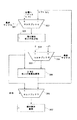
The solution shown in FIG. 3 utilizes a conventional
[0044]
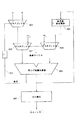
The solution shown in FIG. 4 again uses the conventional
[0045]
The two solutions shown in FIGS. 3 and 4 require separate multiplexer hardware and separate cycles to calculate sticky bits when the preliminary final partial remainder is negative. The
[0046]
In accordance with the present invention, the quotient digit selection logic is modified to prevent the formation of a partial remainder equal to the negative divisor. In order to accurately and effectively calculate the sticky bits that achieve the exact division result, it is necessary to prevent the formation of a negative partial remainder equal to the negative divisor. By strengthening the quotient digit selection function to achieve this, hardware is reduced and waiting time is reduced. For this reason, enhancing the selection function is an ideal solution. Since there is no need to provide an extra mechanism for restoring the preliminary final partial remainder, extra hardware can be eliminated. In addition, since another cycle time for restoring the negative spare partial remainder is not required, the waiting time is shortened.
[0047]
The quotient digit selection logic in accordance with the present invention is modified to select a zero quotient digit instead of a one quotient digit when the actual partial remainder is zero. This is 2PR [i] est This suggests that q [i + 1] = 0 is selected for = 000.0. However, since the quotient digit selection function operates on the predicted partial residue rather than the actual partial residue, careful design of the quotient selection logic is required. Actually, since the predicted partial residue can be less than ½, addition of the lower redundant partial residue bit propagates 1 to the least significant bit position of the upper 4 bits of the actual partial residue. Accordingly, the actual partial remainder is ½ or more.
[0048]
When the actual partial remainder is ½ (or ½ or more), the divisor is limited to ½ ≦ D <1, so it is necessary to always select q = 1. If the actual partial remainder is greater than 1/2 and q = 0 is selected, the next partial remainder shifts the actual partial remainder to the left by one bit without first adding or subtracting the divisor Can be obtained. This left shift forms the next actual partial remainder that exceeds the upper limit of 3/2 required for convergence to an exact quotient.
[0049]
When the exact quotient digit is zero, if the divisor is greater than the actual partial remainder and a value of +1 is selected as the quotient digit, this error can be corrected in a later iteration. However, there is no way to correct this error if zero is selected as the quotient digit when the predicted partial remainder is 000.0 and the exact quotient digit is 1. If q = 0 is selected when q = 1 is the correct quotient digit, there is no way to correct underestimation. The result is an irrecoverable error, and the next partial remainder is outside the predetermined upper and lower limits necessary to converge to an accurate result.
[0050]
Performing binary addition on all partial remainders eliminates the prediction problem. However, this negates the effect on SRT division timing and space. A quotient digit of zero can only be selected when all partial remainders are zero. However, detecting zero for all partial remainders is counterproductive for the same reason.
[0051]
A simple alternative to the above solution is to detect possible carry propagation to the least significant bit of the upper 4 bits of the actual partial remainder. This is the fifth most significant sum and carry bit of the redundant partial remainder, ie PR S, msb-4 And PR C, msb-4 It can be realized by confirming. PR S, msb-4 And PR C, msb-4 Are each zero, carry propagation from that bit position to the least significant bit position of the predicted partial remainder is not possible, and a quotient digit of zero must be selected. In another case where at least one of the fifth most significant carry bit and the sum bit of the redundant partial remainder is 1, it is necessary to select one quotient digit. Even when a plurality of lower bits of the partial remainder are not zero, the partial remainder exists within the predetermined upper and lower limits (−5 / 2 ≦ 2PR ≦ 3/2) and the correct result is still calculated. become.
[0052]
The carry propagation addition necessary for the calculation of the predicted partial residue is performed only on the upper four propagation bits and the sum bit of the actual redundant partial residue. For this reason, the influence on the waiting time of the calculation according to the present invention is minimized. Table 4 shows a truth table for accurate quotient selection logic according to the present invention.
[0053]
[Table 4]
[0054]
The block of
[0055]
The implementation shown in FIG. 5 is logically correct. In practice, however, the 4-bit binary adder and subsequent logic can be integrated and further merged into an optimized logic implementation. As shown in FIG. 6, the five-stage logic implementation uses space more effectively and produces an output with a shorter delay time.
[0056]
In the implementation shown in FIG. 6, M, Z and P are calculated, and logical inversions / M, / Z and / P are also calculated. This is effective when using the quotient signal to enable the transmission gate, such as in a CMOS multiplexer with a decoded select input. M and / M depend only on the upper 4 bits of redundant partial remainder bits (2PRC [msb: msb-3] and 2PRS [msb: msb-3]). On the other hand, Z, P, / Z and / P all depend on the upper 5 bits (2PRC [msb: msb-4] and 2PRS [msb: msb-4]) of the redundant partial remainder. While the cell of FIG. 6 has a second problem of reducing the space occupied by the circuit, it is mainly optimized to minimize delay. Most of the logic shown in FIG. 6 is shared among several output calculations to reduce space.
[0057]
The total number of alternative gates required to implement the new Radix-2 quotient digit selection
[0058]
There is an implementation-dependent timing trade-off between the slower quotient selection logic and the elimination of the last partial residue restoration cycle. If the increase in delay due to slightly more complex quotient selection logic does not limit the Processor cycle time, the increase in performance is due to the reduction in latency cycles required to restore the negative final partial remainder. Always realized. In modern microprocessors, including the hardware divider of the present invention, the processor cycle time is determined by other critical paths, or can be optionally adapted prior to designing the processor. In the case where the increased delay in the quotient selection logic is not the longest path, a net saving of one cycle per divide operation can be realized without additional expense.
[0059]
In the embodiment shown in FIG. 6, the modified quotient selection logic algorithm has optimized the speed of the internal floating point divider critical path using conventional quotient selection rules. About 100 ps slower than the equivalent critical path. This corresponds to a speed reduction of less than 2 percent. The processor's Limiting Timing Path is even longer. Thus, the improved quotient selection logic does not adversely affect processor cycle time. The effect of eliminating the cycle of restoring the partial remainder before sticky detection is realized.
[0060]
Even with the quotient selection logic of the present invention, a negative final partial remainder can still be formed. However, when a negative final partial remainder is formed, the quotient selection logic according to the present invention ensures that the negative partial remainder is greater than the negative divisor. Thus, if a negative final partial remainder according to the present invention is formed, Q-1 is selected and the result will always be inaccurate. As a result, the sticky bit can be safely asserted without fear of the negative final partial remainder being equal to the negative divisor.
[0061]
While code detection and sticky bit calculation are performed in parallel, hardware savings are possible. Instead of using a 59-bit full adder, a 59-bit sign detect adder can be used. While this improves timing slightly, it mainly realizes space savings. Zero detection can be done without the explicit addition of converting redundant partial remainders into binary numbers.
[0062]
[Expression 4]
[0063]
[Equation 5]
[0064]
As mentioned above, although this invention was explained in full detail based on preferable embodiment, the said embodiment is for the purpose of illustration and does not limit this invention. Those skilled in the art can change the embodiments of the present invention as necessary, and the modifications do not depart from the scope and spirit of the present invention disclosed in the claims. For example, the optimized logic implementation of the quotient selection logic shown in FIG. 6 can be designed using various equivalent methods. Also, the circuit shown in FIG. 6 replaces a standard CMOS transmission gate multiplexer with a quotient digit to control an n-channel pass transistor multiplexer. Only the positive polarity can be calculated and the logic inversion calculation can be deleted. Different optimized implementations are the result of implementation in different technologies (eg, NMOS, ECL, etc.) or using different design rules and design tools belonging to the same technology. The claims are intended to cover all circuit implementations of the truth table shown in Table 4. Accordingly, various changes and modifications obvious to those skilled in the art of the present invention belong to the spirit and scope of the present invention.
[0065]
【The invention's effect】
As detailed above, according to the present invention, during floating point division and square root operations, sticky bits can be accurately and effectively calculated when the final partial remainder is negative. Furthermore, the present invention exhibits an excellent effect of reducing the waiting time when executing the quotient selection rule and realizing an optimum quotient selection circuit having a minimum size and a division circuit including the quotient selection circuit. .
[Brief description of the drawings]
FIG. 1 is a simple logic diagram of a conventional hardware division module that implements an iterative SRT division algorithm.
FIG. 2 is a simple logic diagram of a conventional sticky bit arithmetic circuit.
FIG. 3 is a simple logic diagram of one hardware division module that implements an iterative SRT division algorithm or restores a negative final partial remainder.
FIG. 4 is a simple logic diagram of another hardware division module that implements an iterative SRT division algorithm or restores a negative final partial remainder.
FIG. 5 is a simple logic diagram of a circuit that implements the quotient selection rules of the present invention.
FIG. 6 is a detailed logic diagram of a circuit that implements a quotient selection rule that forms a quotient digit signal and its logical inversion.
[Explanation of symbols]
300 ... Carry hold adder, 301, 401 ... Final cycle signal, 302, 303, 306, 403, 402, 405 ... Multiplexer, 304 ... Divisor, 305 ... Register, 307, 406 ... Flip-flop, 400 ... Carry Propagation adder, 404 ... most significant output bit, 404 ... sign bit, 407 ... zero detector, 500 ... 4-bit carry propagation adder, 501 ... all-zero detector, 502 ... all-one detector, 503 ... NAND gate, 504 ... random logic.
Claims (27)
前記第1和ビット、第2和ビット、第3和ビット及び第4和ビット並びに第1桁上げビット、第2桁上げビット、第3桁上げビット及び第4桁上げビットを入力され、そして第1予測部分剰余ビット、第2予測部分剰余ビット、第3予測部分剰余ビット及び第4予測部分剰余ビットを出力として形成する4ビット桁上げ伝搬加算器と、
前記第1予測部分剰余ビット、第2予測部分剰余ビット、第3予測部分剰余ビット及び第4予測部分剰余ビットを入力され、そしてオール・ゼロ信号を形成し、前記オール・ゼロ信号は第1予測部分剰余ビット、第2予測部分剰余ビット、第3予測部分剰余ビット及び第4予測部分剰余ビットが全てゼロの場合にのみアサートされる4ビット・ゼロ検出器と、
前記第1予測部分剰余ビット、第2予測部分剰余ビット、第3予測部分剰余ビット及び第4予測部分剰余ビットを入力され、そしてオール・ワン信号を形成し、前記オール・ワン信号は第1予測部分剰余ビット、第2予測部分剰余ビット、第3予測部分剰余ビット及び第4予測部分剰余ビットが全て1の場合にのみアサートされる4ビット1検出器と、
前記第5和ビット及び第5桁上げビットを入力され、そして第5ビット・ゼロ信号を形成する否定論理和ゲートと、
前記オール・ワン信号、第5ビット・ゼロ信号及びオール・ゼロ信号を入力され、そしてゼロ出力を形成し、前記ゼロ出力はオール・ワン信号がアサートされるか、または第5ビット・ゼロ信号及びオール・ゼロ信号の両方がアサートされた場合にのみアサートされるゼロ回路と
を含む商デジット選択回路。A quotient digit selection circuit for determining a quotient digit in binary division and square root operation based on a redundant partial remainder input, wherein the redundant partial remainder input is a first sum bit, a second sum bit, a third sum bit, A sum bit and a fifth sum bit and a first carry bit, a second carry bit, a third carry bit, a fourth carry bit, and a fifth carry bit, and the selected quotient digit is −1 quotient In a quotient digit selection circuit that is output by asserting one of a negative output corresponding to a digit, a zero output corresponding to a zero quotient digit, and a positive output corresponding to a +1 quotient digit,
The first sum bit, the second sum bit, the third sum bit and the fourth sum bit and the first carry bit, the second carry bit, the third carry bit and the fourth carry bit are input, and A 4-bit carry propagation adder that forms one predicted partial remainder bit, a second predicted partial remainder bit, a third predicted partial remainder bit, and a fourth predicted partial remainder bit;
The first prediction partial residue bit, the second prediction partial residue bit, the third prediction partial residue bit, and the fourth prediction partial residue bit are input and form an all-zero signal, and the all-zero signal is a first prediction. A 4-bit zero detector that is asserted only when the partial remainder bit, the second predicted partial remainder bit, the third predicted partial remainder bit, and the fourth predicted partial remainder bit are all zero;
The first prediction partial residue bit, the second prediction partial residue bit, the third prediction partial residue bit, and the fourth prediction partial residue bit are input and form an all-one signal, and the all-one signal is a first prediction. A 4-bit 1 detector that is asserted only when the partial remainder bit, the second predicted partial residual bit, the third predicted partial residual bit, and the fourth predicted partial residual bit are all 1,
A negative OR gate that receives the fifth sum bit and the fifth carry bit and forms a fifth bit zero signal;
The all-one signal, the fifth bit zero signal and the all-zero signal are input and form a zero output, the zero output is asserted, or the fifth bit zero signal and A quotient digit selection circuit including a zero circuit that is asserted only when both all-zero signals are asserted.
前記第1桁上げビット、第2桁上げビット、第3桁上げビット、第4桁上げビット及び第5桁上げビット並びに第1和ビット、第2和ビット、第3和ビット、第4和ビット及び第5和ビットを入力され、そしてゼロ出力を形成する商ゼロ回路と、
前記第1桁上げビット、第2桁上げビット、第3桁上げビット、第4桁上げビット及び第5桁上げビット並びに第1和ビット、第2和ビット、第3和ビット、第4和ビット及び第5和ビットを入力され、そしてプラス出力を形成する商ポジティブ回路と
を含む商デジット選択回路。A first carry bit, a second carry bit, a third carry bit, a fourth carry bit and a fifth carry bit, and a first sum bit, a second sum bit, a third sum bit, a fourth sum bit, and A quotient digit selection circuit for receiving a fifth sum bit and calculating a quotient digit;
The first carry bit, the second carry bit, the third carry bit, the fourth carry bit, the fifth carry bit, the first sum bit, the second sum bit, the third sum bit, and the fourth sum bit And a quotient zero circuit that receives the fifth sum bit and forms a zero output;
The first carry bit, the second carry bit, the third carry bit, the fourth carry bit, the fifth carry bit, the first sum bit, the second sum bit, the third sum bit, and the fourth sum bit A quotient digit selection circuit including a quotient positive circuit which receives the fifth sum bit and forms a positive output.
前記第1桁上げビット、第2桁上げビット、第3桁上げビット、第4桁上げビット及び第5桁上げビット並びに第1和ビット、第2和ビット、第3和ビット、第4和ビット及び第5和ビットを入力され、そして反転されたプラス出力を形成する反転商ポジティブ回路と、
前記第1桁上げビット、第2桁上げビット、第3桁上げビット及び第4桁上げビット並びに第1和ビット、第2和ビット、第3和ビット及び第4和ビットを入力され、そして反転されたマイナス出力を形成する反転商ネガティブ回路と
を含む請求項7に記載の商デジット選択回路。The first carry bit, the second carry bit, the third carry bit, the fourth carry bit, the fifth carry bit, the first sum bit, the second sum bit, the third sum bit, and the fourth sum bit And an inverted quotient zero circuit which receives the fifth sum bit and forms an inverted zero output;
The first carry bit, the second carry bit, the third carry bit, the fourth carry bit, the fifth carry bit, the first sum bit, the second sum bit, the third sum bit, and the fourth sum bit And an inverted quotient positive circuit that receives the fifth sum bit and forms an inverted positive output;
The first carry bit, the second carry bit, the third carry bit, the fourth carry bit, the first sum bit, the second sum bit, the third sum bit, and the fourth sum bit are input and inverted. The quotient digit selection circuit according to claim 7, further comprising an inverted quotient negative circuit for forming a negative output.
オペランド除数を第1の反復中に入力され、そして出力として除数を形成する除数レジスタと、
請求項7に記載の商デジット選択回路と、
前記部分剰余と、商デジット及び除数の否定論理積とを入力され、そして左シフトされた部分剰余を形成する加算器と
を含む浮動小数点正規形仮数除算回路。A partial remainder register in which the dividend is input during the first iteration and then the left-shifted partial remainder is input during subsequent iterations and forms a partial remainder as an output;
A divisor register that receives an operand divisor during the first iteration and forms a divisor as an output;
A quotient digit selection circuit according to claim 7,
A floating-point normal mantissa division circuit including the partial remainder and an adder that inputs a quotient digit and a negative logical product of a divisor and forms a left-shifted partial remainder.
第1予測部分剰余ビット、第2予測部分剰余ビット、第3予測部分剰余ビット及び第4予測部分剰余ビットを形成すべく第1和ビット、第2和ビット、第3和ビット及び第4和ビットを第1桁上げビット、第2桁上げビット、第3桁上げビット及び第4桁上げビットに対して加算する工程と、
前記第1予測部分剰余ビット、第2予測部分剰余ビット、第3予測部分剰余ビット及び第4予測部分剰余ビットが全て1である場合、または前記第1予測部分剰余ビット、第2予測部分剰余ビット、第3予測部分剰余ビット及び第4予測部分剰余ビットが全てゼロであって、かつ第5和ビット及び第5桁上げビットの両方がゼロに等しい場合にのみ商デジットとしてゼロを選択する工程と
を含む方法。A method of selecting a quotient digit from redundant partial remainders in binary division and square root operations, wherein the redundant partial remainders are a first sum bit, a second sum bit, a third sum bit, a fourth sum bit, and a fifth sum bit. And a method comprising a first carry bit, a second carry bit, a third carry bit, a fourth carry bit, and a fifth carry bit,
A first sum bit, a second sum bit, a third sum bit, and a fourth sum bit to form a first prediction partial remainder bit, a second prediction partial remainder bit, a third prediction partial remainder bit, and a fourth prediction partial remainder bit Adding to the first carry bit, the second carry bit, the third carry bit, and the fourth carry bit;
The first prediction partial residue bit, the second prediction partial residue bit, the third prediction partial residue bit, and the fourth prediction partial residue bit are all 1, or the first prediction partial residue bit and the second prediction partial residue bit Selecting zero as the quotient digit only if the third predicted partial remainder bit and the fourth predicted partial remainder bit are all zero and both the fifth sum bit and the fifth carry bit are equal to zero; Including methods.
前記第1和ビット、第2和ビット、第3和ビット及び第4和ビット並びに第1桁上げビット、第2桁上げビット、第3桁上げビット及び第4桁上げビットを入力され、そして第1予測部分剰余ビット、第2予測部分剰余ビット、第3予測部分剰余ビット及び第4予測部分剰余ビットを出力として形成する4ビット桁上げ伝搬加算器を形成する工程と、
前記第1予測部分剰余ビット、第2予測部分剰余ビット、第3予測部分剰余ビット及び第4予測部分剰余ビットを入力され、そしてオール・ゼロ信号を形成し、前記オール・ゼロ信号は第1予測部分剰余ビット、第2予測部分剰余ビット、第3予測部分剰余ビット及び第4予測部分剰余ビットが全てゼロの場合にのみアサートされる4ビット・ゼロ検出器を形成する工程と、
前記第1予測部分剰余ビット、第2予測部分剰余ビット、第3予測部分剰余ビット及び第4予測部分剰余ビットを入力され、そしてオール・ワン信号を形成し、前記オール・ワン信号は第1予測部分剰余ビット、第2予測部分剰余ビット、第3予測部分剰余ビット及び第4予測部分剰余ビットが全て1の場合にのみアサートされる4ビット1検出器を形成する工程と、
前記第5和ビット及び第5桁上げビットを入力され、そして第5ビット・ゼロ信号を形成する否定論理和ゲートを形成する工程と、
前記オール・ワン信号、第5ビット・ゼロ信号及びオール・ゼロ信号を入力され、そしてゼロ出力を形成し、前記ゼロ出力はオール・ワン信号がアサートされるか、または第5ビット・ゼロ信号及びオール・ゼロ信号の両方がアサートされた場合にのみアサートされるゼロ回路を形成する工程と
を含む方法。A method of forming a quotient digit selection circuit for determining a quotient digit in binary division and square root operation based on a redundant partial remainder input, wherein the redundant partial remainder input is a first sum bit, a second sum bit, a third sum The selected quotient digit comprising a bit, a fourth sum bit and a fifth sum bit and a first carry bit, a second carry bit, a third carry bit, a fourth carry bit and a fifth carry bit Is output by asserting one of a negative output corresponding to a -1 quotient digit, a zero output corresponding to a zero quotient digit, and a positive output corresponding to a +1 quotient digit.
The first sum bit, the second sum bit, the third sum bit and the fourth sum bit and the first carry bit, the second carry bit, the third carry bit and the fourth carry bit are input, and Forming a 4-bit carry propagation adder that forms one predicted partial remainder bit, a second predicted partial remainder bit, a third predicted partial remainder bit, and a fourth predicted partial remainder bit;
The first prediction partial residue bit, the second prediction partial residue bit, the third prediction partial residue bit, and the fourth prediction partial residue bit are input and form an all-zero signal, and the all-zero signal is a first prediction. Forming a 4-bit zero detector that is asserted only when the partial remainder bit, the second predicted partial residual bit, the third predicted partial residual bit, and the fourth predicted partial residual bit are all zero;
The first prediction partial residue bit, the second prediction partial residue bit, the third prediction partial residue bit, and the fourth prediction partial residue bit are input and form an all-one signal, and the all-one signal is a first prediction. Forming a 4-bit 1 detector that is asserted only when the partial remainder bit, the second predicted partial residual bit, the third predicted partial residual bit, and the fourth predicted partial residual bit are all 1,
Forming a negative OR gate that receives the fifth sum bit and the fifth carry bit and forms a fifth bit zero signal;
The all-one signal, the fifth bit zero signal and the all-zero signal are input and form a zero output, the zero output is asserted, or the fifth bit zero signal and Forming a zero circuit that is asserted only when both all-zero signals are asserted.
前記第1桁上げビット、第2桁上げビット、第3桁上げビット、第4桁上げビット及び第5桁上げビット並びに第1和ビット、第2和ビット、第3和ビット、第4和ビット及び第5和ビットを入力され、そしてゼロ出力を形成する商ゼロ回路を形成する工程と、
前記第1桁上げビット、第2桁上げビット、第3桁上げビット、第4桁上げビット及び第5桁上げビット並びに第1和ビット、第2和ビット、第3和ビット、第4和ビット及び第5和ビットを入力され、そしてプラス出力を形成する商ポジティブ回路を形成する工程と
を含む方法。A first carry bit, a second carry bit, a third carry bit, a fourth carry bit and a fifth carry bit, and a first sum bit, a second sum bit, a third sum bit, a fourth sum bit, and A method of forming a quotient digit selector that receives a fifth sum bit and calculates a quotient digit comprising:
The first carry bit, the second carry bit, the third carry bit, the fourth carry bit, the fifth carry bit, the first sum bit, the second sum bit, the third sum bit, and the fourth sum bit And forming a quotient zero circuit that receives the fifth sum bit and forms a zero output;
The first carry bit, the second carry bit, the third carry bit, the fourth carry bit, the fifth carry bit, the first sum bit, the second sum bit, the third sum bit, and the fourth sum bit And forming a quotient positive circuit that receives the fifth sum bit and forms a positive output.
前記第1桁上げビット、第2桁上げビット、第3桁上げビット、第4桁上げビット及び第5桁上げビット並びに第1和ビット、第2和ビット、第3和ビット、第4和ビット及び第5和ビットを入力され、そして反転されたプラス出力を形成する反転商ポジティブ回路を形成する工程と、
前記第1桁上げビット、第2桁上げビット、第3桁上げビット及び第4桁上げビット並びに第1和ビット、第2和ビット、第3和ビット及び第4和ビットを入力され、そして反転されたマイナス出力を形成する反転商ネガティブ回路を形成する工程と
を含む請求項22に記載の方法。The first carry bit, the second carry bit, the third carry bit, the fourth carry bit, the fifth carry bit, the first sum bit, the second sum bit, the third sum bit, and the fourth sum bit And forming an inverted quotient zero circuit receiving the fifth sum bit and forming an inverted zero output;
The first carry bit, the second carry bit, the third carry bit, the fourth carry bit, the fifth carry bit, the first sum bit, the second sum bit, the third sum bit, and the fourth sum bit And forming an inverted quotient positive circuit receiving the fifth sum bit and forming an inverted positive output;
The first carry bit, the second carry bit, the third carry bit, the fourth carry bit, the first sum bit, the second sum bit, the third sum bit, and the fourth sum bit are input and inverted. Forming an inverted quotient negative circuit for forming a negative output.
オペランド除数を第1の反復中に入力され、そして出力として除数を形成する除数レジスタを形成する工程と、
請求項22に記載の商デジット選択回路を形成する工程と、
前記部分剰余と、商デジット及び除数の否定論理積とを入力され、そして左シフトされた部分剰余を形成する加算器を形成する工程と
を含む浮動小数点正規形仮数除算回路を形成する方法。Forming a partial remainder register in which the dividend is input during a first iteration and then the left-shifted partial remainder is input during subsequent iterations and forms a partial remainder as an output;
Forming a divisor register in which an operand divisor is input during the first iteration and forms a divisor as an output;
Forming a quotient digit selection circuit according to claim 22;
A method of forming a floating-point normal mantissa division circuit including the step of forming an adder that receives the partial remainder and the NAND of the quotient digit and the divisor and forms a left-shifted partial remainder.
Applications Claiming Priority (2)
| Application Number | Priority Date | Filing Date | Title |
|---|---|---|---|
| US08/498,397 US5787030A (en) | 1995-07-05 | 1995-07-05 | Correct and efficient sticky bit calculation for exact floating point divide/square root results |
| US08/498397 | 1995-07-05 |
Publications (2)
| Publication Number | Publication Date |
|---|---|
| JPH0934691A JPH0934691A (en) | 1997-02-07 |
| JP3689183B2 true JP3689183B2 (en) | 2005-08-31 |
Family
ID=23980922
Family Applications (1)
| Application Number | Title | Priority Date | Filing Date |
|---|---|---|---|
| JP16750896A Expired - Fee Related JP3689183B2 (en) | 1995-07-05 | 1996-06-27 | Accurate and effective sticky bit calculation for accurate floating-point division / square root operations |
Country Status (3)
| Country | Link |
|---|---|
| US (2) | US5787030A (en) |
| JP (1) | JP3689183B2 (en) |
| KR (1) | KR100323338B1 (en) |
Cited By (1)
| Publication number | Priority date | Publication date | Assignee | Title |
|---|---|---|---|---|
| TWI754680B (en) * | 2016-11-03 | 2022-02-11 | 南韓商三星電子股份有限公司 | Apparatus and method of generating starting estimate, manufacturing method and testing method |
Families Citing this family (56)
| Publication number | Priority date | Publication date | Assignee | Title |
|---|---|---|---|---|
| US5995992A (en) * | 1997-11-17 | 1999-11-30 | Bull Hn Information Systems Inc. | Conditional truncation indicator control for a decimal numeric processor employing result truncation |
| US6594681B1 (en) * | 1998-11-04 | 2003-07-15 | Sun Microsystems, Inc. | Quotient digit selection logic for floating point division/square root |
| US6732135B1 (en) * | 1999-02-01 | 2004-05-04 | Hewlett-Packard Development Company, L.P. | Method and apparatus for accumulating partial quotients in a digital processor |
| US6360241B1 (en) * | 1999-02-01 | 2002-03-19 | Compaq Information Technologies Goup, L.P. | Computer method and apparatus for division and square root operations using signed digit |
| JP2002063025A (en) * | 2000-08-18 | 2002-02-28 | Fujitsu Ltd | Variable length data processing processor |
| JP3793505B2 (en) * | 2000-09-26 | 2006-07-05 | 株式会社ルネサステクノロジ | Arithmetic unit and electronic circuit device using the same |
| US7031996B2 (en) * | 2000-11-02 | 2006-04-18 | Seagate Technology Llc | Calculating square root of binary numbers with fixed-point microprocessor |
| US6792443B2 (en) * | 2001-06-29 | 2004-09-14 | Intel Corporation | Economical on-the-fly rounding for digit-recurrence algorithms |
| EP1315080A1 (en) * | 2001-11-22 | 2003-05-28 | STMicroelectronics Limited | Circuitry for carrying out square root and division operations |
| EP1315079A1 (en) * | 2001-11-22 | 2003-05-28 | STMicroelectronics Limited | Circuit for calculation of division and square root with floating point numbers |
| EP1315081B1 (en) * | 2001-11-22 | 2008-05-07 | STMicroelectronics Limited | Circuitry for carrying out at least one of a square root operation and a division operation |
| EP1315082A1 (en) | 2001-11-22 | 2003-05-28 | STMicroelectronics Limited | Iteration circuitry for carrying out square root operation on floating point numbers |
| EP1315077A1 (en) * | 2001-11-23 | 2003-05-28 | STMicroelectronics Limited | Circuitry and method for performing floating point compare operations |
| US7127483B2 (en) * | 2001-12-26 | 2006-10-24 | Hewlett-Packard Development Company, L.P. | Method and system of a microprocessor subtraction-division floating point divider |
| AU2003212146A1 (en) * | 2002-03-13 | 2003-09-22 | The University Of British Columbia | High dynamic range display devices |
| US7016930B2 (en) * | 2002-10-25 | 2006-03-21 | Arm Limited | Apparatus and method for performing operations implemented by iterative execution of a recurrence equation |
| US7660842B2 (en) * | 2003-05-12 | 2010-02-09 | Sun Microsystems, Inc. | Method and apparatus for performing a carry-save division operation |
| US7139786B2 (en) * | 2003-05-12 | 2006-11-21 | Sun Microsystems, Inc. | Method and apparatus for efficiently performing a square root operation |
| US7216216B1 (en) | 2004-06-30 | 2007-05-08 | Sun Microsystems, Inc. | Register window management using first pipeline to change current window and second pipeline to read operand from old window and write operand to new window |
| US8095778B1 (en) | 2004-06-30 | 2012-01-10 | Open Computing Trust I & II | Method and system for sharing functional units of a multithreaded processor |
| US7353364B1 (en) | 2004-06-30 | 2008-04-01 | Sun Microsystems, Inc. | Apparatus and method for sharing a functional unit execution resource among a plurality of functional units |
| US7533248B1 (en) | 2004-06-30 | 2009-05-12 | Sun Microsystems, Inc. | Multithreaded processor including a functional unit shared between multiple requestors and arbitration therefor |
| US7178005B1 (en) | 2004-06-30 | 2007-02-13 | Sun Microsystems, Inc. | Efficient implementation of timers in a multithreaded processor |
| US7343474B1 (en) | 2004-06-30 | 2008-03-11 | Sun Microsystems, Inc. | Minimal address state in a fine grain multithreaded processor |
| US7426630B1 (en) | 2004-06-30 | 2008-09-16 | Sun Microsystems, Inc. | Arbitration of window swap operations |
| US7370243B1 (en) | 2004-06-30 | 2008-05-06 | Sun Microsystems, Inc. | Precise error handling in a fine grain multithreaded multicore processor |
| US7373489B1 (en) | 2004-06-30 | 2008-05-13 | Sun Microsystems, Inc. | Apparatus and method for floating-point exception prediction and recovery |
| US7437538B1 (en) | 2004-06-30 | 2008-10-14 | Sun Microsystems, Inc. | Apparatus and method for reducing execution latency of floating point operations having special case operands |
| US7434000B1 (en) | 2004-06-30 | 2008-10-07 | Sun Microsystems, Inc. | Handling duplicate cache misses in a multithreaded/multi-core processor |
| US7523330B2 (en) * | 2004-06-30 | 2009-04-21 | Sun Microsystems, Inc. | Thread-based clock enabling in a multi-threaded processor |
| US7383403B1 (en) | 2004-06-30 | 2008-06-03 | Sun Microsystems, Inc. | Concurrent bypass to instruction buffers in a fine grain multithreaded processor |
| US7702887B1 (en) | 2004-06-30 | 2010-04-20 | Sun Microsystems, Inc. | Performance instrumentation in a fine grain multithreaded multicore processor |
| US7890734B2 (en) * | 2004-06-30 | 2011-02-15 | Open Computing Trust I & II | Mechanism for selecting instructions for execution in a multithreaded processor |
| US7861063B1 (en) | 2004-06-30 | 2010-12-28 | Oracle America, Inc. | Delay slot handling in a processor |
| US7478225B1 (en) | 2004-06-30 | 2009-01-13 | Sun Microsystems, Inc. | Apparatus and method to support pipelining of differing-latency instructions in a multithreaded processor |
| US7185178B1 (en) | 2004-06-30 | 2007-02-27 | Sun Microsystems, Inc. | Fetch speculation in a multithreaded processor |
| US7941642B1 (en) | 2004-06-30 | 2011-05-10 | Oracle America, Inc. | Method for selecting between divide instructions associated with respective threads in a multi-threaded processor |
| US8225034B1 (en) | 2004-06-30 | 2012-07-17 | Oracle America, Inc. | Hybrid instruction buffer |
| US7774393B1 (en) | 2004-06-30 | 2010-08-10 | Oracle America, Inc. | Apparatus and method for integer to floating-point format conversion |
| US7401206B2 (en) * | 2004-06-30 | 2008-07-15 | Sun Microsystems, Inc. | Apparatus and method for fine-grained multithreading in a multipipelined processor core |
| US7330988B2 (en) * | 2004-06-30 | 2008-02-12 | Sun Microsystems, Inc. | Method and apparatus for power throttling in a multi-thread processor |
| US7676655B2 (en) * | 2004-06-30 | 2010-03-09 | Sun Microsystems, Inc. | Single bit control of threads in a multithreaded multicore processor |
| US7747771B1 (en) | 2004-06-30 | 2010-06-29 | Oracle America, Inc. | Register access protocol in a multihreaded multi-core processor |
| US8037250B1 (en) | 2004-12-09 | 2011-10-11 | Oracle America, Inc. | Arbitrating cache misses in a multithreaded/multi-core processor |
| JP4273071B2 (en) * | 2004-12-15 | 2009-06-03 | エヌイーシーコンピュータテクノ株式会社 | Divide and square root calculator |
| US7539720B2 (en) * | 2004-12-15 | 2009-05-26 | Sun Microsystems, Inc. | Low latency integer divider and integration with floating point divider and method |
| US7752250B2 (en) * | 2006-01-12 | 2010-07-06 | International Business Machines Corporation | Rounding floating point division results |
| EP2118880A4 (en) * | 2007-02-01 | 2010-08-25 | Dolby Lab Licensing Corp | Calibration of displays having spatially-variable backlight |
| US8024719B2 (en) | 2008-11-03 | 2011-09-20 | Advanced Micro Devices, Inc. | Bounded hash table sorting in a dynamic program profiling system |
| US20100115494A1 (en) * | 2008-11-03 | 2010-05-06 | Gorton Jr Richard C | System for dynamic program profiling |
| US8478948B2 (en) * | 2008-12-04 | 2013-07-02 | Oracle America, Inc. | Method and system for efficient tracing and profiling of memory accesses during program execution |
| US20100214282A1 (en) * | 2009-02-24 | 2010-08-26 | Dolby Laboratories Licensing Corporation | Apparatus for providing light source modulation in dual modulator displays |
| US8452831B2 (en) * | 2009-03-31 | 2013-05-28 | Oracle America, Inc. | Apparatus and method for implementing hardware support for denormalized operands for floating-point divide operations |
| US8817875B2 (en) * | 2009-08-13 | 2014-08-26 | The Johns Hopkins University | Methods and systems to encode and decode sequences of images |
| US9086890B2 (en) | 2012-01-06 | 2015-07-21 | Oracle International Corporation | Division unit with normalization circuit and plural divide engines for receiving instructions when divide engine availability is indicated |
| US10706101B2 (en) | 2016-04-14 | 2020-07-07 | Advanced Micro Devices, Inc. | Bucketized hash tables with remap entries |
Family Cites Families (5)
| Publication number | Priority date | Publication date | Assignee | Title |
|---|---|---|---|---|
| US5023827A (en) * | 1988-08-18 | 1991-06-11 | Digital Equipment Corporation | Radix-16 divider using overlapped quotient bit selection and concurrent quotient rounding and correction |
| US5272660A (en) * | 1992-06-01 | 1993-12-21 | Motorola, Inc. | Method and apparatus for performing integer and floating point division using a single SRT divider in a data processor |
| US5386376A (en) * | 1992-08-31 | 1995-01-31 | Intel Corporation | Method and apparatus for overriding quotient prediction in floating point divider information processing systems |
| US5258944A (en) * | 1992-09-01 | 1993-11-02 | Cray Research, Inc. | High performance mantissa divider |
| US5357455A (en) * | 1992-10-09 | 1994-10-18 | Intel Corporation | Floating point remainder generator for a math processor |
-
1995
- 1995-07-05 US US08/498,397 patent/US5787030A/en not_active Expired - Fee Related
-
1996
- 1996-05-15 US US08/648,410 patent/US5954789A/en not_active Expired - Lifetime
- 1996-06-27 JP JP16750896A patent/JP3689183B2/en not_active Expired - Fee Related
- 1996-07-03 KR KR1019960026783A patent/KR100323338B1/en not_active IP Right Cessation
Cited By (1)
| Publication number | Priority date | Publication date | Assignee | Title |
|---|---|---|---|---|
| TWI754680B (en) * | 2016-11-03 | 2022-02-11 | 南韓商三星電子股份有限公司 | Apparatus and method of generating starting estimate, manufacturing method and testing method |
Also Published As
| Publication number | Publication date |
|---|---|
| US5787030A (en) | 1998-07-28 |
| KR970008882A (en) | 1997-02-24 |
| KR100323338B1 (en) | 2002-06-22 |
| JPH0934691A (en) | 1997-02-07 |
| US5954789A (en) | 1999-09-21 |
Similar Documents
| Publication | Publication Date | Title |
|---|---|---|
| JP3689183B2 (en) | Accurate and effective sticky bit calculation for accurate floating-point division / square root operations | |
| US6594681B1 (en) | Quotient digit selection logic for floating point division/square root | |
| Obermann et al. | Division algorithms and implementations | |
| EP0450754B1 (en) | High speed dividers | |
| US6847985B1 (en) | Floating point divide and square root processor | |
| US5696712A (en) | Three overlapped stages of radix-2 square root/division with speculative execution | |
| Zhang et al. | Efficient multiple-precision floating-point fused multiply-add with mixed-precision support | |
| JP3609512B2 (en) | Computing unit | |
| Lang et al. | A radix-10 digit-recurrence division unit: algorithm and architecture | |
| US5132925A (en) | Radix-16 divider using overlapped quotient bit selection and concurrent quotient rounding and correction | |
| US5023827A (en) | Radix-16 divider using overlapped quotient bit selection and concurrent quotient rounding and correction | |
| Bruguera | Low latency floating-point division and square root unit | |
| US6941334B2 (en) | Higher precision divide and square root approximations | |
| Bruguera | Radix-64 floating-point divider | |
| EP0436905B1 (en) | High performance adder using carry predictions | |
| US7016930B2 (en) | Apparatus and method for performing operations implemented by iterative execution of a recurrence equation | |
| US6598065B1 (en) | Method for achieving correctly rounded quotients in algorithms based on fused multiply-accumulate without requiring the intermediate calculation of a correctly rounded reciprocal | |
| US7127483B2 (en) | Method and system of a microprocessor subtraction-division floating point divider | |
| Dixit et al. | FPGA accomplishment of a 16-bit divider | |
| US7660842B2 (en) | Method and apparatus for performing a carry-save division operation | |
| US6615228B1 (en) | Selection based rounding system and method for floating point operations | |
| Baesler et al. | FPGA implementation of a decimal floating-point accurate scalar product unit with a parallel fixed-point multiplier | |
| JPH04172526A (en) | Floating point divider | |
| Bashagha et al. | Radix digit-serial pipelined divider/square-root architecture | |
| US5208769A (en) | Unsigned integer multiply/divide circuit |
Legal Events
| Date | Code | Title | Description |
|---|---|---|---|
| A977 | Report on retrieval |
Free format text: JAPANESE INTERMEDIATE CODE: A971007 Effective date: 20050428 |
|
| TRDD | Decision of grant or rejection written | ||
| A01 | Written decision to grant a patent or to grant a registration (utility model) |
Free format text: JAPANESE INTERMEDIATE CODE: A01 Effective date: 20050517 |
|
| A61 | First payment of annual fees (during grant procedure) |
Free format text: JAPANESE INTERMEDIATE CODE: A61 Effective date: 20050610 |
|
| R150 | Certificate of patent or registration of utility model |
Free format text: JAPANESE INTERMEDIATE CODE: R150 |
|
| LAPS | Cancellation because of no payment of annual fees |